
CCD e CID per Rivelazione di Radiazione...
21
CCD e CID per Rivelazione di Radiazione Infrarossa
Transcript of CCD e CID per Rivelazione di Radiazione...
CCDeCIDperRivelazionediRadiazioneInfrarossa
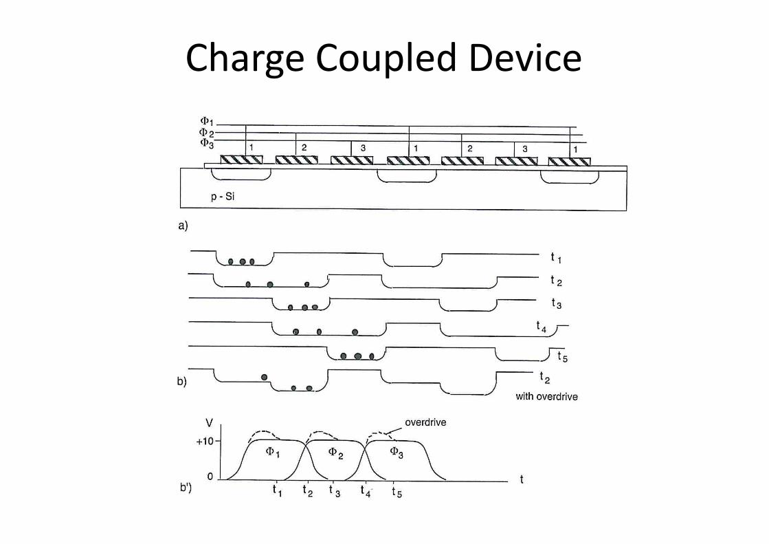
ChargeCoupledDevice
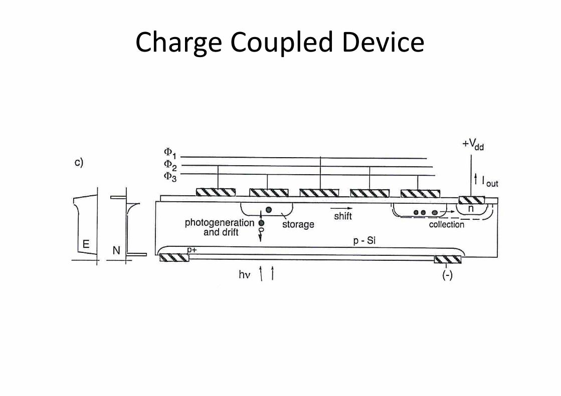
ChargeCoupledDevice
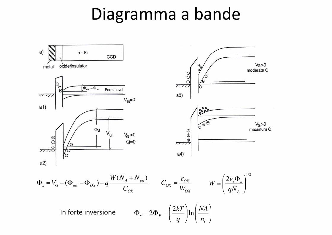
Diagrammaabande
Φs =VG − (Φms −ΦOX )− qW (NA + Nph )
COX
COX =εOXWOX
W =2εsΦs
qNA
"
#$
%
&'
1/2
Φs = 2ΦF =2kTq
"
#$
%
&'ln
NAni
"
#$
%
&'Inforteinversione
ΦOX −Φms

Saturazione
BCCD
Campoelettricodibreakdown
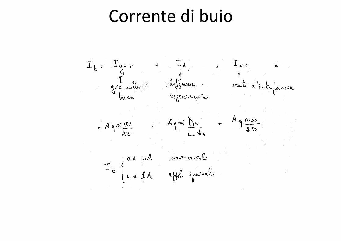
Correntedibuio
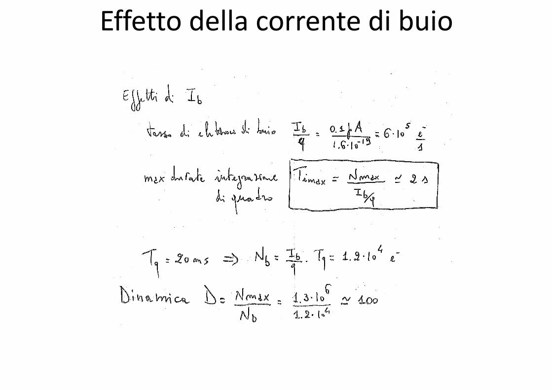
Effettodellacorrentedibuio
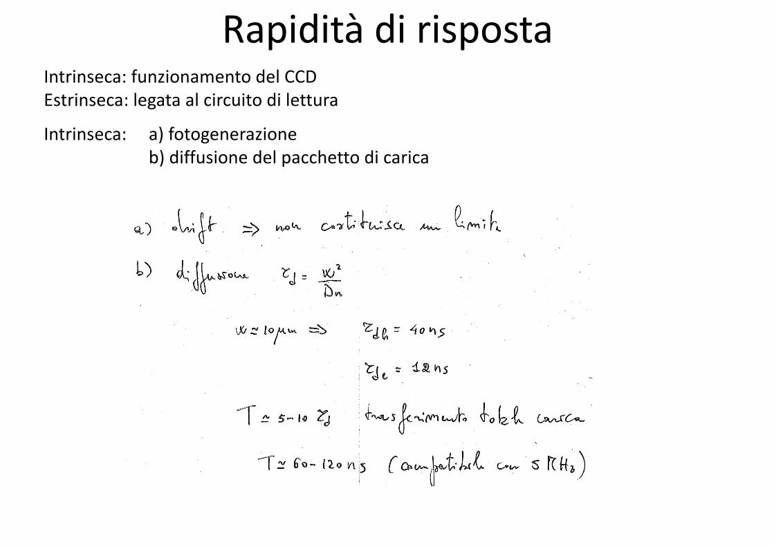
RapiditàdirispostaIntrinseca:funzionamentodelCCDEstrinseca:legataalcircuitodilettura
Intrinseca: a)fotogenerazioneb)diffusionedelpacchettodicarica
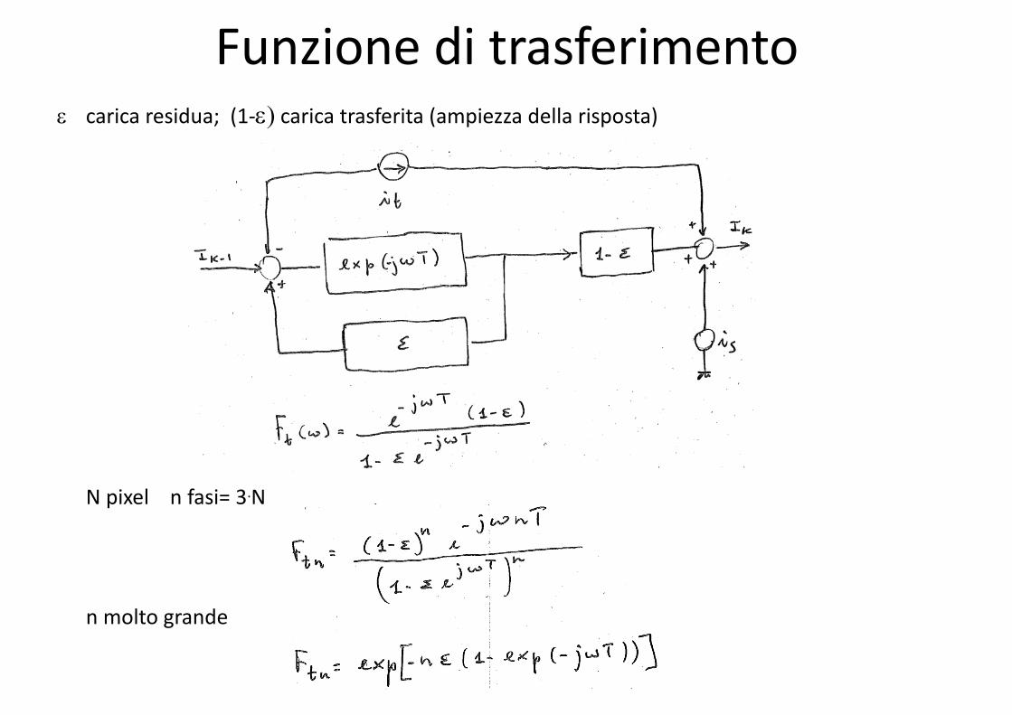
Funzioneditrasferimento
Npixelnfasi=3.N
nmoltogrande
e caricaresidua;(1-e) caricatrasferita(ampiezzadellarisposta)
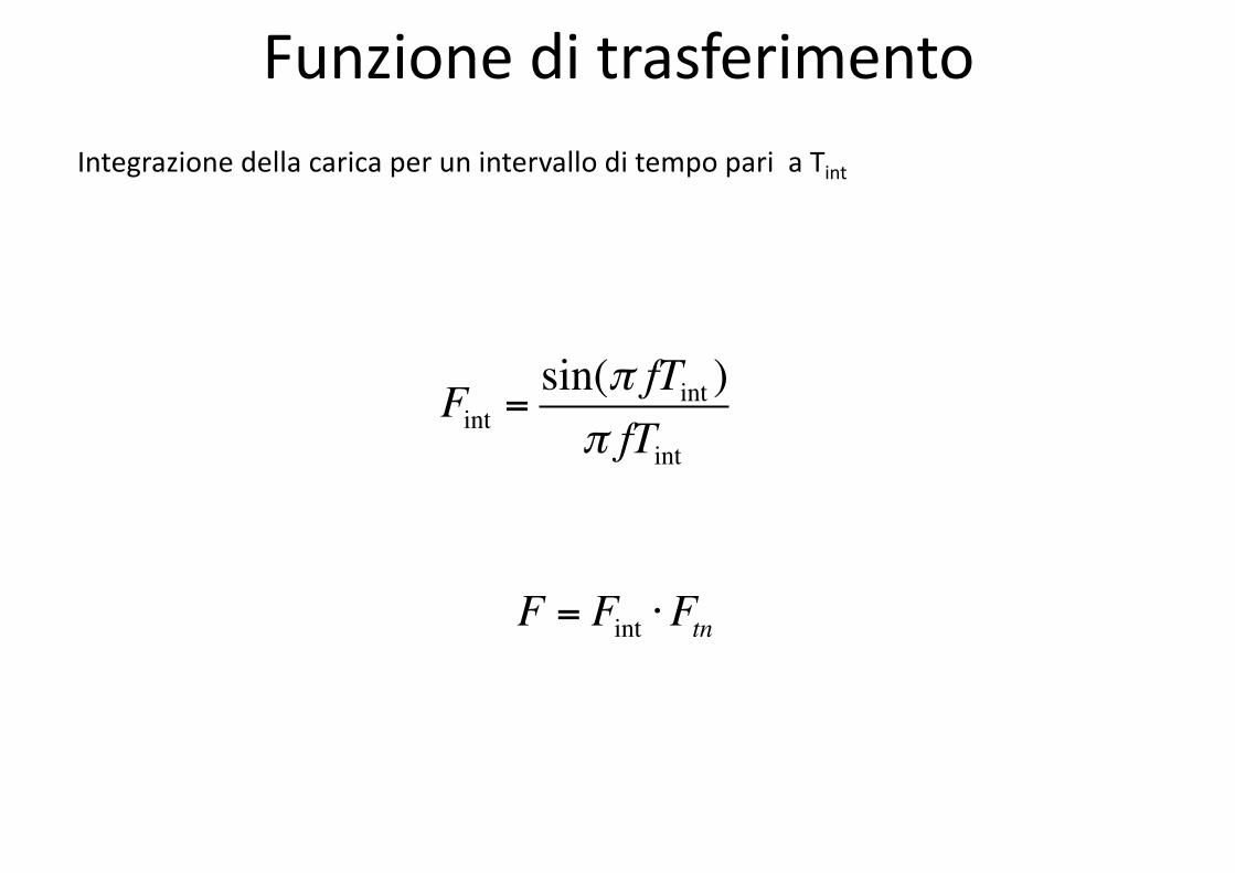
FunzioneditrasferimentoIntegrazionedellacaricaperunintervalloditempopariaTint
Fint =sin(π fTint )π fTint
F = Fint ⋅Ftn
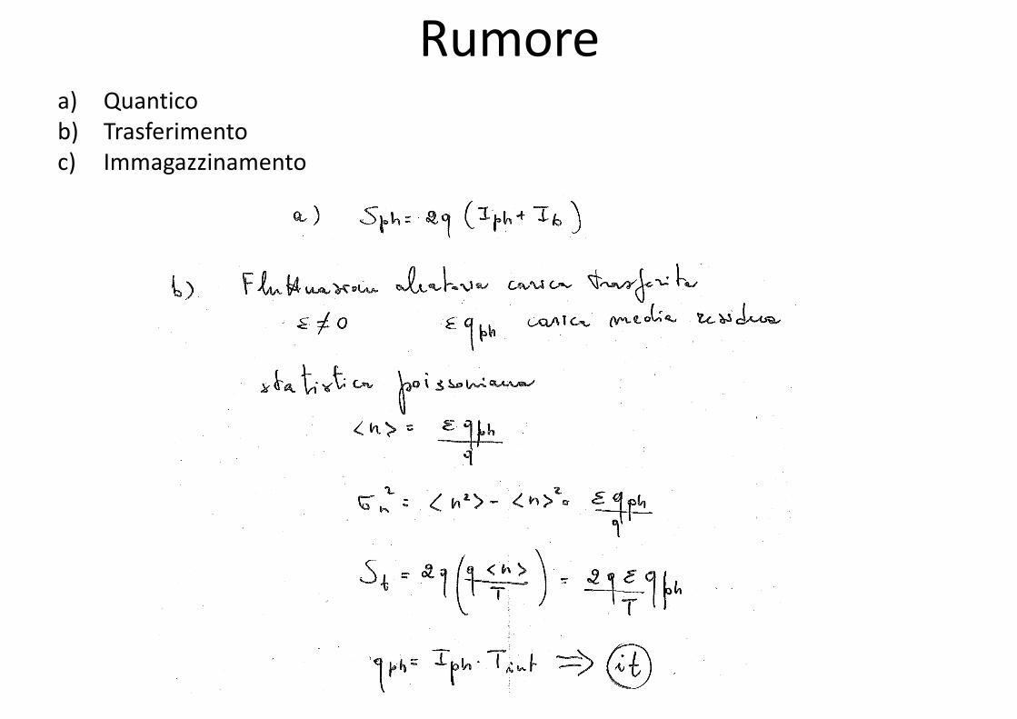
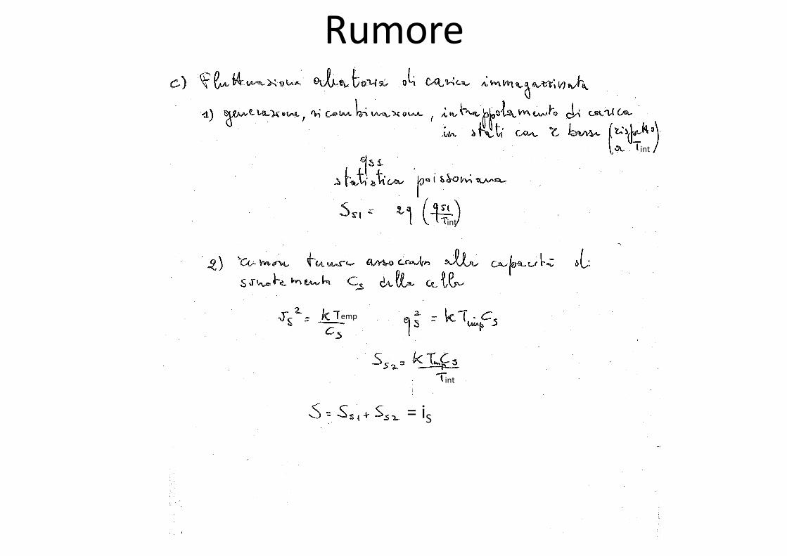
Rumorea) Quanticob) Trasferimentoc) Immagazzinamento
Rumore
int
int
int
int
int
int
=iS
emp
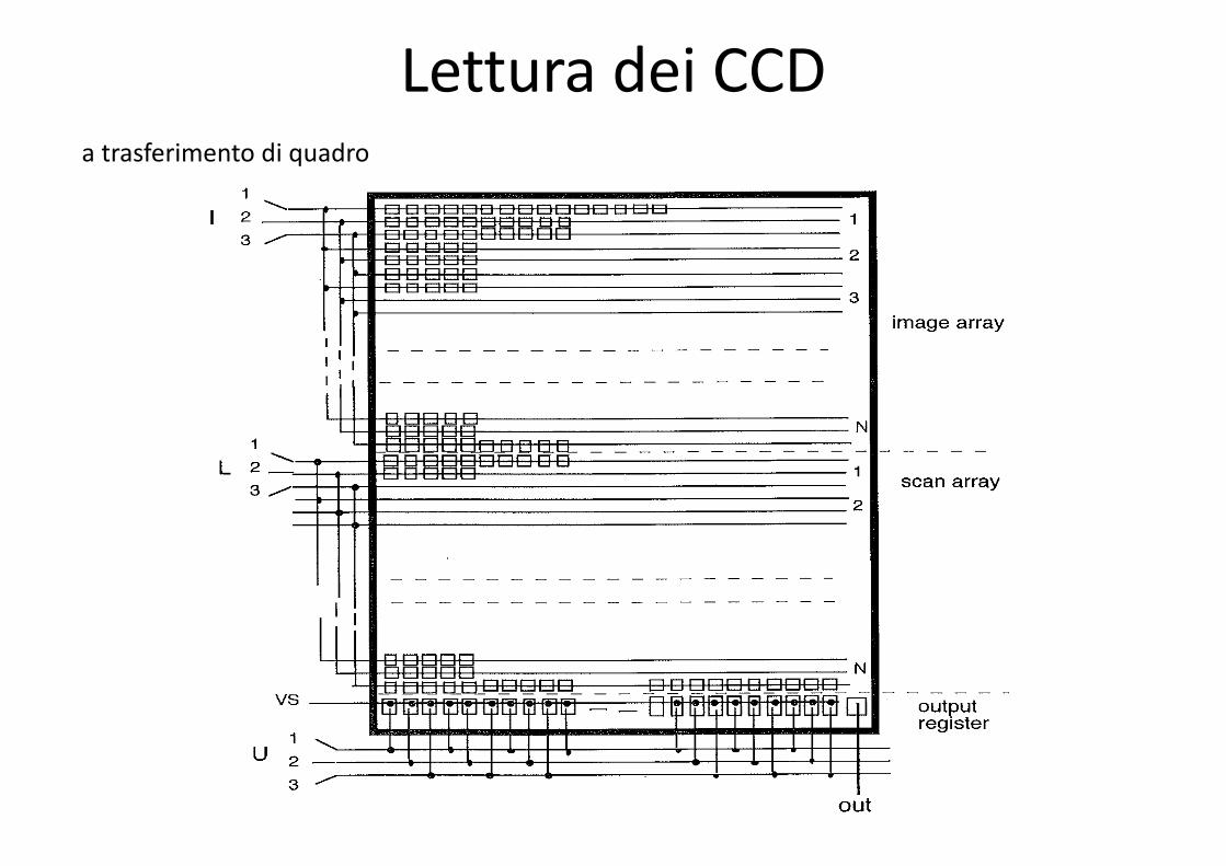
LetturadeiCCDatrasferimentodiquadro
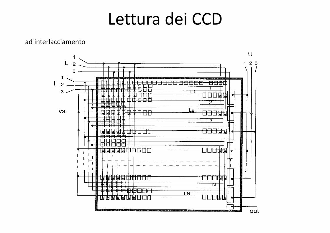
LetturadeiCCDadinterlacciamento
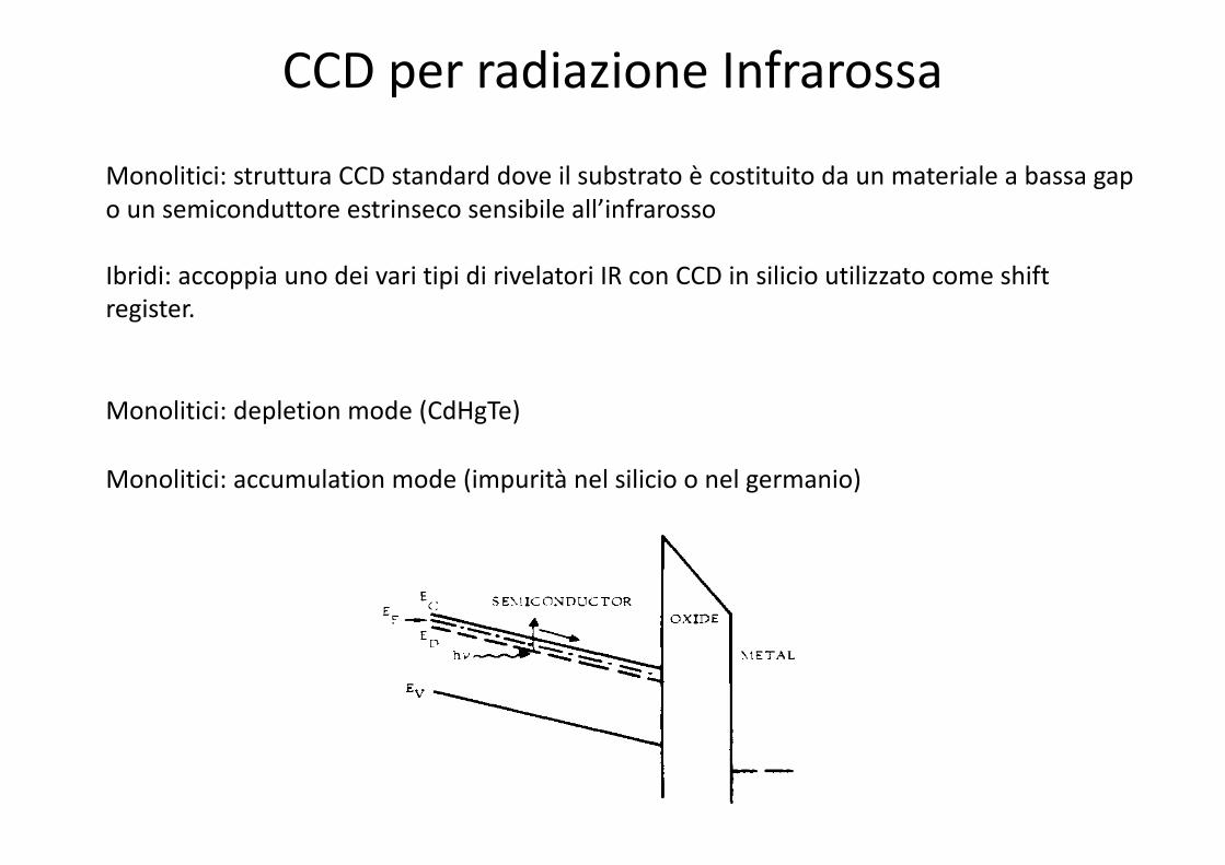
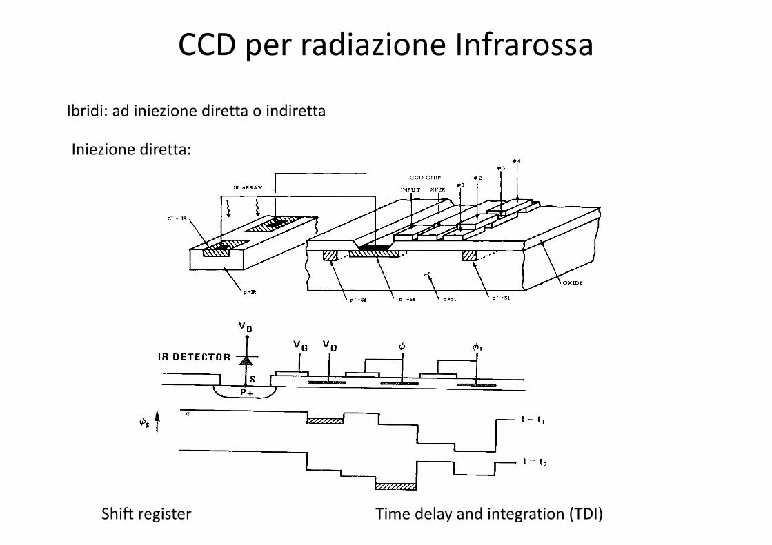
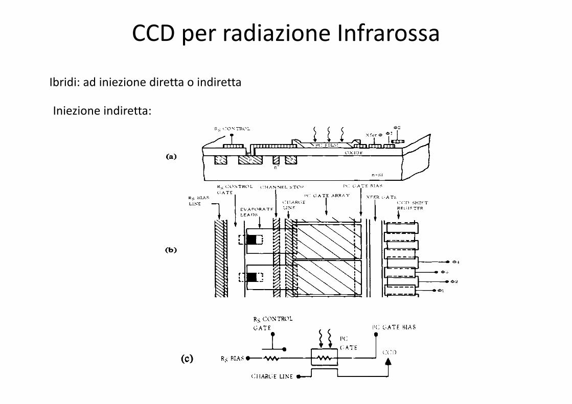
CCDperradiazioneInfrarossa
Monolitici:strutturaCCDstandarddoveilsubstratoècostituitodaunmaterialeabassagapounsemiconduttoreestrinsecosensibileall’infrarosso
Ibridi:accoppiaunodeivaritipidirivelatoriIRconCCDinsilicioutilizzatocomeshiftregister.
Monolitici:depletionmode(CdHgTe)
Monolitici:accumulationmode(impuritànelsilicioonelgermanio)STECKL e ta l . : CCD’s FOR INFRARED DETECTION AND IMAGING 71
Fig. 2. Energy band diagram for an MIS structure biased into accumulation.
nology and extend it to the IR region. However, to minimize the thermal generation current, temperatures below impurity freezeout are generally required. Fig. 2 shows the energy band bending in an accumulation-mode MIS structure at a sub- freezeout temperature. The bands have a linear spatial be- havior through the semiconductor substrate due to the absence of space charge. The large spatial penetration of the electric field gives rise to considerable fringing fields [ 151 which en- hance the charge transfer efficiency [ 221, [ 231 . Furthermore, the electric field at an accumulated semiconductor surface is much smaller than at an inverted surface because the surface potential appears across the whole thickness of the substrate, rather than only a thin depletion layer. As a consequence, the width of the accumulation layer charge packet is as much as an order of magnitude greater than an inversion layer packet. Accumulation-mode devices built and investigated by our laboratory [3] have a four-phase two-layer overlapping-gate structure. A 64-cell n-channel device was built on a lO%m-’ phosphorous-silicon substrate. The observed transfer efficiency was 0.99 per gate at a chip frequency of 25 kHz and a temper- ature of 4.2 K. Calculations [3] for this device indicate a charge packet depth of 300 A. Having the charge stored at this distance from the interface reduces the importance of surface trapping states and, hence, further aids transfer efficiency.
C. Schottky-Barrier Photoemissive Devices Another approach to solving the nonuniformity limitations
of monolithic IRCCD devices, as proposed by Sheperd and Yang [4] , is based on internal photoemission from metal- semiconductor Schottky-barrier arrays on a silicon substrate. The photoemission process is shown in Fig. 3(a): photons of energy hv < E, are absorbed in the metal resulting in the ex- citation of a hot carrier. Carriers with energy larger than the contact barrier and with sufficient momentum in that direction are emitted into the semiconductor. The depletion iegion set up by the application of a reverse-bias voltage is diminished in size by the emitted carriers neutralizing the immobile charges at its edge [Fig. 3(b)]. The photoemitted current is, therefore, integrated by a negative charge accumulation method. The readout of the Schottky-barrier detector into the CCD takes place via an MOS transfer gate which converts the initial ma- jority carrier signal into the minority carrier transport required by the Si CCD (Fig. 4).
The Schottky-barrier IRCCD has several main features: a) the use of silicon and its well-known properties as the basis for the entire device; b) the use of photodetection in a metal film, resulting in highly uniform responsivity across a typical array (approximately 1 percent [4] ), as well as excellent re- producibility from array to array (approximately 1 percent [24]); c) the photoemissive yield is still relatively low, 7
Fig. 3. Internal photoemission in a Schottky-barrier detector [ 4 ] . (a) Energy band diagram. (b) Device operation.
L H A R G E C E K
T R A S S F m CLCX’K
62 63
Fig. 4. Schottky-barrier IRCCD proposed by Sheperd and Yang 141.
1 percent at X = 3.1 pm and T = 77 K for Au-p-Si contacts W I . D. Other Monolithic Devices
Other monolithic IRCCD’s receiving attention include: a) Germanium-substrate CCD [ 261. By substituting Ge for Si, one extends the intrinsic CCD response in the near infrared out to about 1.8 pm. A 10sell Ge CCD reported by Schroder [26] has been operated over the temperature range of 100 to 265 K at clock frequencies of 10 to 300 kHz. Transfer effi- ciencies of 95 percent without background charge and 97.5 percent with 20-percent charge have been measured. b) Charge injection devices [ 271, [ 281 use injection into the bulk for readout rather than the sequential transfer principle of CCD, and, therefore, fal l in a different category of devices. Infrared applications of CID’s include the work of Kim [28] with InSb.
IV. HYBRID IRCCDs Since the hybrid IRCCD involves the coupling of two already
fairly well developed technologies, it has received more atten- tion [ 51, [ 291 -[ 3 1 ] to date than the monolithic concept. As mentioned in Section I, hybrid IRCCD’s fall into two cate- gories: direct and indirect injection devices.
A . Direct Injection Devices In the direct injection IRCCD, the photogenerated charge is
directly introduced into the CCD shift register [SI. Since this is in effect a dc coupled system, only those detectors with very small dc currents (e.g., photovoltaic, extrinsic detectors) can be fed into the CCD, due to the latter’s limited charge handling capacity. The basic direct injection concept is illustrated in Fig. 5 for an n-on-p IR photodiode and an nchannel CCD. The IR photodiode is connected in parallel to a silicon coupling diode (SCD) diffused into the same silicon substrate on which the CCD is fabricated. The first MOS gate (input) of the CCD is used to reverse-bias the IR diode and the silicon coupling diode; the TRANSFER gate is used to introduce the photocharge into the CCD through a field induced nshannel. When the 61 gate is activated with a positive pulse, the PO-
72 PROCEEDINGS OF THE IEEE, JANUARY 1975
IR A M Y INPUT XFER I
I \ \ \ \ Y \ \ \ ,
GATE INPUT XFER 1 U
INPUT !llI’I~USlC~U
(b) Fa. 5. Direct injection hybrid IRCCD. (a) Coupling concept. (b) Array layout.
tential well under the gate acts as a sink for the diodes and the photocurrent plus the saturation currents of the diodes will flow into the well for the duration of the $1 pulse. When the $2 gate is turned on and the $1 gate is turned off, the current flow stops and the charge present is transferred on through the device.
Direct injection devices being investigated in the Electronics Research Division laboratory [321 include an InSb diode array coupled to a 10tLbit p-chanael CCD shift register through eight input taps. Both the detector array and the CCD have been operated at an 80 K temperature. Direct injection has been observed for CCD chip frequencies up to and higher than 1 MHz.
A potential application of the direct injection hybrid IRCCD is in the serially scanned TV-compatible Forward Looking Infrared (FLIR) system (cf. Milton [33]) . The serially scanned FLIR uses a linear array of detectors raster-scanned across the scene, the scan direction being parallel to the array. Since each detector in turn scans the entire field of view, the dwell time per resolution element is approximately 150 ns. The amount of charge generated during this dwell time in even an 8-14-pm IR detector by a 300 K blackbody is well within the charge handling capacity of a typical CCD shift register. By processing the outputs of the detectors through a delay- and-add operation, the components of the signals correspond- ing to the same resolution element are summed linearly. Be- cause the noise contribution of each detector is independent
and thus uncorrelated, the total noise is obtained by an r m s summation. For an array of m detectors, the delay-and-add operation could, therefore, result in a maximum improvement of fi (in the detector noise limited case) in the signal-to-noise ratio (SNR) of the entire array over that of an individual d e tector. The upper limit of m and, therefore, of the maximum SNR improvement achievable is set by the total detector array signal versus the CCD charge capacity. The operation of the entire array appears at the CCD output essentially as one de- tector. This results in no fixed pattern noise, lowered detector response uniformity requirements, as well as built-in re- dundancy. These features together with the potential fi improvement in SNR help circumvent the problems posed by the high background and low-contrast ratio present in thermal imaging systems at IR wavelengths.
An SNR analysk for a direct injection hybrid IRCCD oper- ated in the delay-and-add mode was developed by Steckl and Koehler [ 51. For a typical application consisting of an array of nine 12-pm (Hg, Cd) Te photodiodes receiving an incident flux of 3 X 10’’ photons/cm2 - s (TB = 300 K, FOV = 90°), they calculate an SNR of 500, a dynamic range of 300, and a noise equivalent change in temperature of 0.1 K.
B. Indirect Injection Devices Indirect injection hybrid IRCCD’s use a buffer stage between
the photodetection stage and the CCD shift register. The buffer stage can vary from one on-chip MOSFET to a number
CCDperradiazioneInfrarossa
Ibridi:adiniezionedirettaoindiretta
Iniezionediretta:
Shiftregister Timedelayandintegration(TDI)
CCDperradiazioneInfrarossa
Ibridi:adiniezionedirettaoindiretta
Iniezioneindiretta:STECKL etal.: CCD’s FOR INFRARED DETECTION AND IMAGING 73
of off-chip amplifiers. It is the simplest version that is more appealing in its simplicity and ease of integration. Two in- direct injection devices, one using pyroelectric detectors and the other photoconductive (PC) thin films, are discussed here.
I ) Indirect Injection-Photoconductive Films: A technique which can be utilized with any photoconducting film which can be deposited on silicon dioxide without inducing fast states (or interface traps) at the silicon-silicon dioxide inter- face is described. The photoconductive film is used to directly influence the inversion of the channel of the input MOSFET. The degree of inversion, in turn, controls the rate of charge flow into the CCD. The photoconductive gate device is shown in Fig. 6. The advantage of this method is that the photo- conductive fiim can be deposited by a variety of techniques after all the silicon MOS CCD process steps have been performed.
Operation of the device is described by the following se- quence of steps.
1) A voltage is applied to the R , bias line. This voltage has to be large enough to invert the oxide-semiconductor inter- face underneath the photosensitive elements.
2) A voltage is applied to the R, control gate to provide an appropriate resistance in series with the photoconductive gate.
3) The PC gate bias is set just above the threshold value of voltage for this gate. This results in the transfer of maximum charge in the absence of optical input signal, thus providing blooming protection for the device.
4) Incident photons cause the resistance of the PC films to decrease accordingly. This causes a drop in the voltage across each PC film inversely proportional to the local density of incident photons.
5 ) The charge passing into the CCD is now a function of the illumination level falling upon the PC film. The response of the device to optical signal transients is governed by the ability of the biasing resistor to discharge the PC gate capacitance.
This device scheme, while hybrid and indirect, provides a straightforward and relatively easily fabricated method of IRCCD imaging. 2) Indirect Injection-Pyroelectric Detectors: Pyroelectric
materials owe their photodetection property to a temperature- dependent polarization (for a review of pyroelectric detectors, see Putley [ 351). In the steady state, the polarization is masked by surface charges and, therefore, the incident radiation must be chopped. This results in ac coupled detection and thus background subtraction. Additional features of pyroelec- tric detectors are inexpensive detector materials and room- temperature operation. However, the sensitivity of present pyroelectric detectors is considerably lower than that of quantum detectors.
Detection of the thermally induced electric polarization of the pyroelectric is accomplished by making the pyroelectric the dielectric of a capacitor. Two methods of introducing the pyroelectric signal into a CCD are 1) connecting the capacitor to an on-chip MOSFET or 2) fabricating a pyroelectric film be- tween the MOSFET channel and the gate metal (viz., in series with the gate). Both methods are essentially the same, the latter requiring more sophgticated processing, but resulting in a more compact structure, as illustrated in Fig. 7. The device uses the voltage developed by the pyroelectric detector to modulate the “potential well” depth in an MOS structure and, in so doing, affects a charge transfer modulation in the charge carriers generated thermally and flowing to an adjacent deeper
Rg RIAS LIVE
(.AT1
1 t
Fig. 6. Indirect injection: photoconductive thin-fdm hybrid IRCCD. (a) Device cross section. (b) Two-dimensional layout. (c) Equivalent circuit.
pJ k l pJ ! I--1 !
CCDmANNFL I Fig. 7. Indirect injection: pyroelectric hybrid IRCCD.
but smaller area potential well in a CCD multiplexer which “passes by” the modulated well. The voltage Vo is con- stant and just large enough to make the well several kT in depth. Charge (generated mainly by the surface states) keeps the well essentially full. The “drain” is over the N potential bamer and into the CCD channel. The voltages are adjusted until the modulation due to the scene (there is a shutter which modulates the incident radiation) is not “clipped” by the dark current flow and the dark current is equal to that required for essentially 1 00-percent modulation of the scene.
A first-order noise analysis of the device indicates I361 that the dominant noise contribution is the Johnson noise associ- ated with the detector and input circuit. For a typical applica- tion, an IRCCD operating at 20 frames/s and using triglycine sulphate cells of 10-’-cm2 area placed on an oxide of 60GA thickness should result in a minimum resolvable temperature of about 0.3 K in the 8-12-pm window. It should be noted that in order to achieve this predicted performance in practical devices, a high degree of thermal isolation is required in order to prevent thermal loading by the substrate as well as inter- element crosstalk.
STECKL etal.: CCD’s FOR INFRARED DETECTION AND IMAGING 73
of off-chip amplifiers. It is the simplest version that is more appealing in its simplicity and ease of integration. Two in- direct injection devices, one using pyroelectric detectors and the other photoconductive (PC) thin films, are discussed here.
I ) Indirect Injection-Photoconductive Films: A technique which can be utilized with any photoconducting film which can be deposited on silicon dioxide without inducing fast states (or interface traps) at the silicon-silicon dioxide inter- face is described. The photoconductive film is used to directly influence the inversion of the channel of the input MOSFET. The degree of inversion, in turn, controls the rate of charge flow into the CCD. The photoconductive gate device is shown in Fig. 6. The advantage of this method is that the photo- conductive fiim can be deposited by a variety of techniques after all the silicon MOS CCD process steps have been performed.
Operation of the device is described by the following se- quence of steps.
1) A voltage is applied to the R , bias line. This voltage has to be large enough to invert the oxide-semiconductor inter- face underneath the photosensitive elements.
2) A voltage is applied to the R, control gate to provide an appropriate resistance in series with the photoconductive gate.
3) The PC gate bias is set just above the threshold value of voltage for this gate. This results in the transfer of maximum charge in the absence of optical input signal, thus providing blooming protection for the device.
4) Incident photons cause the resistance of the PC films to decrease accordingly. This causes a drop in the voltage across each PC film inversely proportional to the local density of incident photons.
5 ) The charge passing into the CCD is now a function of the illumination level falling upon the PC film. The response of the device to optical signal transients is governed by the ability of the biasing resistor to discharge the PC gate capacitance.
This device scheme, while hybrid and indirect, provides a straightforward and relatively easily fabricated method of IRCCD imaging. 2) Indirect Injection-Pyroelectric Detectors: Pyroelectric
materials owe their photodetection property to a temperature- dependent polarization (for a review of pyroelectric detectors, see Putley [ 351). In the steady state, the polarization is masked by surface charges and, therefore, the incident radiation must be chopped. This results in ac coupled detection and thus background subtraction. Additional features of pyroelec- tric detectors are inexpensive detector materials and room- temperature operation. However, the sensitivity of present pyroelectric detectors is considerably lower than that of quantum detectors.
Detection of the thermally induced electric polarization of the pyroelectric is accomplished by making the pyroelectric the dielectric of a capacitor. Two methods of introducing the pyroelectric signal into a CCD are 1) connecting the capacitor to an on-chip MOSFET or 2) fabricating a pyroelectric film be- tween the MOSFET channel and the gate metal (viz., in series with the gate). Both methods are essentially the same, the latter requiring more sophgticated processing, but resulting in a more compact structure, as illustrated in Fig. 7. The device uses the voltage developed by the pyroelectric detector to modulate the “potential well” depth in an MOS structure and, in so doing, affects a charge transfer modulation in the charge carriers generated thermally and flowing to an adjacent deeper
Rg RIAS LIVE
(.AT1
1 t
Fig. 6. Indirect injection: photoconductive thin-fdm hybrid IRCCD. (a) Device cross section. (b) Two-dimensional layout. (c) Equivalent circuit.
pJ k l pJ ! I--1 !
CCDmANNFL I Fig. 7. Indirect injection: pyroelectric hybrid IRCCD.
but smaller area potential well in a CCD multiplexer which “passes by” the modulated well. The voltage Vo is con- stant and just large enough to make the well several kT in depth. Charge (generated mainly by the surface states) keeps the well essentially full. The “drain” is over the N potential bamer and into the CCD channel. The voltages are adjusted until the modulation due to the scene (there is a shutter which modulates the incident radiation) is not “clipped” by the dark current flow and the dark current is equal to that required for essentially 1 00-percent modulation of the scene.
A first-order noise analysis of the device indicates I361 that the dominant noise contribution is the Johnson noise associ- ated with the detector and input circuit. For a typical applica- tion, an IRCCD operating at 20 frames/s and using triglycine sulphate cells of 10-’-cm2 area placed on an oxide of 60GA thickness should result in a minimum resolvable temperature of about 0.3 K in the 8-12-pm window. It should be noted that in order to achieve this predicted performance in practical devices, a high degree of thermal isolation is required in order to prevent thermal loading by the substrate as well as inter- element crosstalk.
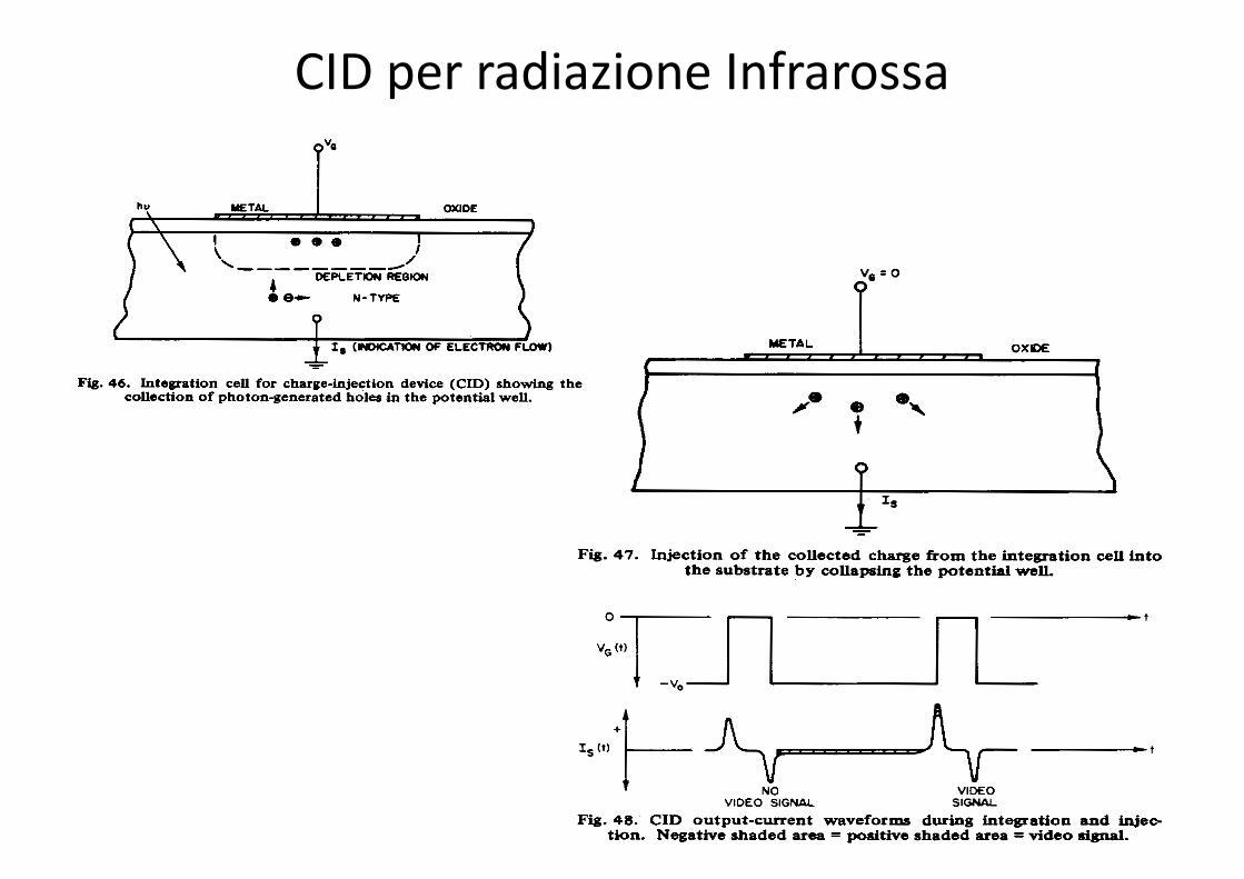
CIDperradiazioneInfrarossa
58 PROCEEDINGS OF THE IEEE, JANUARY 1975
(a) (b) ( 4 Fig. 45. Photographs showing CCD imagery. (a) Noncontiguous horizontal integration cells. (b) Simulated
contiguous horizontal integration cells. (c) Simulated overlapping horizontal integration cells.
0 0 0 ; ----_--- /' 1 0 e+ N-TYPE
DEPLETW REGION
P Is ~INDICATKYI OF ELECTRON FLOW) - -
Fig. 46. Integration cell for charge-injection device (CID) showing the collection of photon-generated holes in the potential well.
are collected in the wells, as shown in Fig. 46. The charge con- configuration in the potential wells is a point-by-point sampling of the light falling on the image plane. Thus the integration process in a CID is the same as that in a CCD.
For video signal readout, the charge stored in a potential well is injected into the bulk at the end of the integration time by removing the gate voltage, as shown in Fig. 47. These minority carriers recombine at the substrate contact thereby causing a current flow in the external circuit. The details of the current flow during integration and readout are described in the fol-
As a drive voltage pulse is applied to the gate, a depletion re- gion is formed, creating majority carriers, electrons in this case, flowing through the substrate. Because of capacitance cou- pling both positive and negative pulses of substrate current will result in the waveform, shown in Fig. 48. During integration, photongenerated minority carriers, holes in this case, will be collected at the surface in the potential well and stored as shown in Fig. 46, while the photongenerated electrons will continuously flow through the substrate, as shown by the nega- tive shaded area of the substrate current curve in Fig. 48. At the end of the frame time, the injection of the stored charges wiU increase the positive pulse height, as shown in the second
lowing paragraphs.
P v, = 0
Fig. 47. Injection of the collected charge from the integration cell into the substrate by collapsing the potential well.
I No VIDEO SIGNAL
VIDEO SIGNAL
Fig. 48. CID output-current waveforms during integration and W e tion. Negative shaded area = positive shaded area = video dgd.
pulses of Fig. 48, which constitutes the desired video informa- tion. The integration of this current waveform results in a net signal proportional to the injected video charge. The net volt- age is sampled to provide the video output signal.
For two-dimensional CID arrays, the structure requires two separate metal electrodes per unit cell, in order to scan the ar- ray elements in the x-y direction. The two-dimensional opera- tion of this device is illustrated in Fig. 49. Each sensor element consists of two separate electrodes for two storage capacitors.
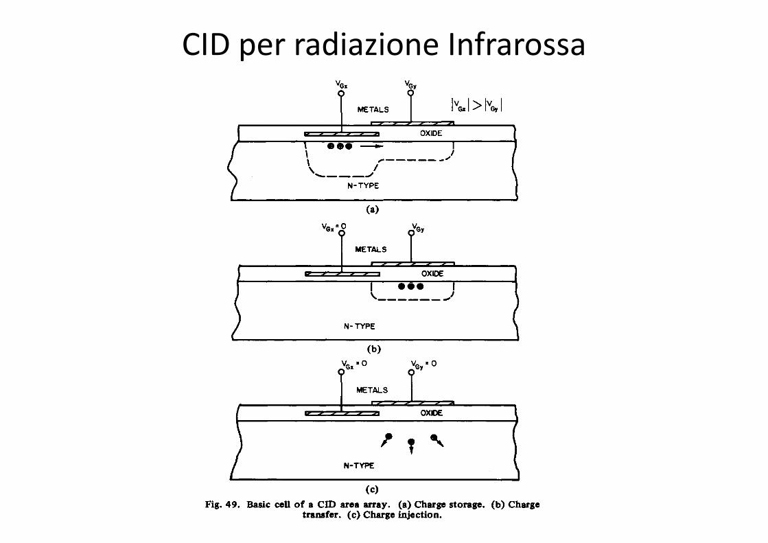
CIDperradiazioneInfrarossaBARBE: CHARGECOUPLED IMAGING DEVICES 59
N-TYPE I
p””” voy = 0
P
? ? % N-TYPE
I (4
Fig. 49. Basic cell of a CID area array. (a) Charge storage. (b) Charge transfer. (c) Charge injection.
One of the electrodes is connected to a horizontal access line, the other to a vertical line.
Fig. 49(a) shows the normal charge storage in the potential well; as the one electrode in the particular cell shown is turned off, the stored charges under that electrode are transferred to the other potential well, as shown in Fig. 49(b). The injection of the stored charge in the particular sensor cell will occur only when both electrode voltages are switched off, as demonstrated in F i g . 49(c); therefore, a sensor element is sampled only when both the electrode voltages are removed from the sampling cell.
The CID is simpler to fabricate than the CCD. The CID is x-y addressed and therefore lends itself to random access. The CCD readout is serial. The output capacitance of a CID is the capacitance of one row and one column if all other rows and columns are floated during the readout of a given cell. The output capacitance of a CCD is the capacitance of a reverse- biased diode. Therefore, the process of reading out a CID is noisier than that of reading out a CCD.
C. Further ZYadeoffs and State of the Art There are other comparisons that can be made between
BIFT, F IR , and CID imaging a r r a y s . A thinned and backside- passivated frame-transfer chip can be operated in the electron- bombarded inducedanductivity (EBIC) mode. This provides a preintegration gain; however, high voltages (in the kilovolt range) are required. Also, it is not clear that a CCD can with- stand bakeout in vacuum and long-tenn operation in vacuum without degradation. The interline-transfer design is incom- patible with backside-illumination or EBIC mode operation. It
Fig. 50. Relative response versus wavelength for an FIIT area array.
TABLE VI11 AREA IMAGING CHIP PARAMETERS
isnot clear whether the CID will be efficient in the EBIC mode of operation due to the conflicting constraints that high recom- bination is required at the backside of the chip for efficient CID readout whereas low recombination is required for effi- cient collection of carriers generated by photoelectron absorp- tion. The non-EBIC approach to low-light-level imaging is cooled buried-channel photonexcited arrays with low-noise amplifiers.
Another factor in comparing area arrays is the spectral re- sponse. The response of a backside photon-illuminated linear device is shown in Fig. 31. The response of a frontside- illuminated interline-transfer area array is shown in Fig. 50. The structure is caused by interference effects in the layered frontside structure. The shape of the response can be altered in the frontside-illuminated case by choice of layer thicknesses during fabrication.
Most of the area arrays that have been fabricated are front- side illuminated, although Texas Instruments has imaged with a backside-illuminated 64 by 64 array. Table VI11 summarizes the area arrays that have been fabricated.
D. Performance Predictions In the noise-limited region, the noise-limited resolution R is
proportional to the elemental signal-to-noise ratio. Using the “average-current” formulation, the signal is CHSA rinteg/e, where C is the contrast. The photon noise is (HSA tinteg/e)1/2 and the total CCD noise is N . Then [2 1 I
R = K CHSA tinteg/e (HSA tinteg/e + N2)lI2 *
It has been shown empirically with low-light-level imaging tubes that patterns having bar lengths extending over one- third of the picture height can be resolved at mean photoelec-
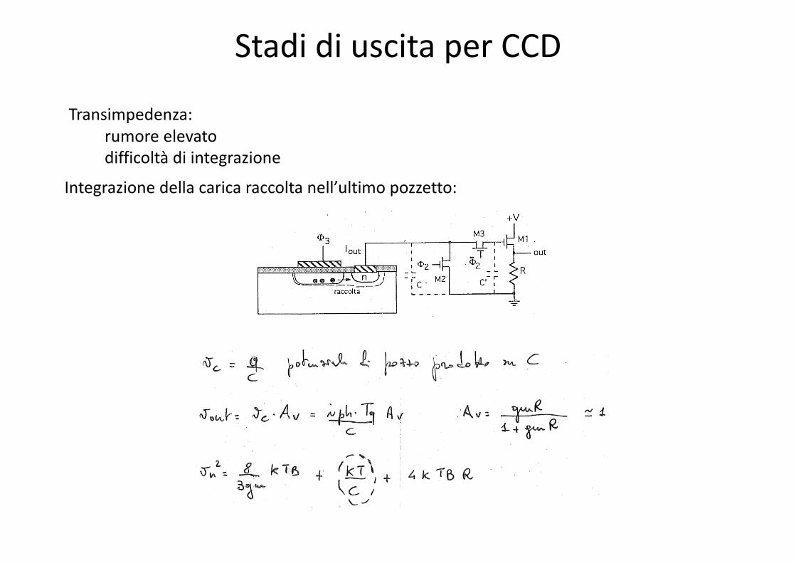
StadidiuscitaperCCD
Transimpedenza:rumoreelevatodifficoltàdiintegrazione
Integrazionedellacaricaraccoltanell’ultimopozzetto:
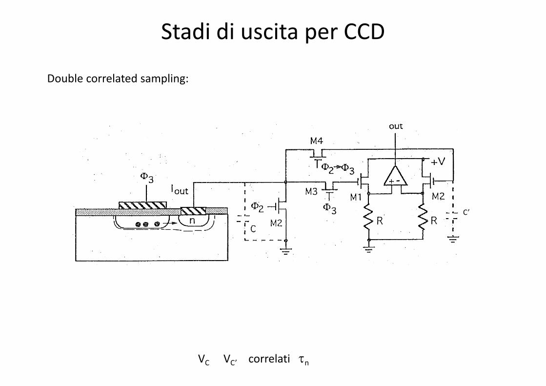
StadidiuscitaperCCD
Doublecorrelatedsampling:
C’
VC VC’ correlatitn


![H-254 COSTRUZIONI IDRAULICHE - manualihoepli.it · H-254 COSTRUZIONI IDRAULICHE Dove: Lg = larghezza della griglia [m] E = energia della corrente [m] ε = grado di apertura delle](https://static.fdocument.org/doc/165x107/5c65fa8609d3f2c14e8b67d7/h-254-costruzioni-idrauliche-h-254-costruzioni-idrauliche-dove-lg-larghezza.jpg)