Advanced Power Electronics Corp. (20130401)… · 1 Advanced Power Electronics Corp. AP431A...
10
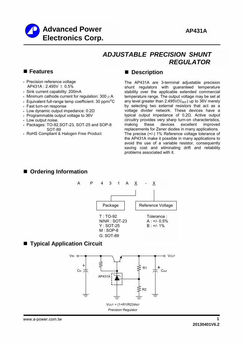
www.a-power.com.tw 1 Advanced Power Electronics Corp. AP431A Features • Precision reference voltage AP431A : 2.495V ± 0.5% • Sink current capability: 200mA • Minimum cathode current for regulation: 300μA • Equivalent full-range temp coefficient: 30 ppm/ o C • Fast turn-on response • Low dynamic output impedance: 0.2Ω • Programmable output voltage to 36V • Low output noise. • Packages: TO-92,SOT-23, SOT-25 and SOP-8 • RoHS Compliant & Halogen Free Product Description The AP431A are 3-terminal adjustable precision shunt regulators with guaranteed temperature stability over the applicable extended commercial temperature range. The output voltage may be set at any level greater than 2.495V(V REF ) up to 36V merely by selecting two external resistors that act as a voltage divider network. These devices have a typical output impedance of 0.2Ω. Active output circuitry provides very sharp turn-on characteristics, making these devices excellent improved replacements for Zener diodes in many applications. The precise (+/-) 1% Reference voltage tolerance of the AP431A make it possible in many applications to avoid the use of a variable resistor, consequently saving cost and eliminating drift and reliability problems associated with it. Ordering Information Typical Application Circuit + + R2 R1 VOUT VIN VOUT = (1+R1/R2)V REF Precision Regulator Cin Cout AP431A ADJUSTABLE PRECISION SHUNT REGULATOR A P 4 3 1 A X - X Package Reference Voltage T : TO-92 N/NR : SOT-23 Y : SOT-25 M : SOP-8 Tolerance : A : +/- 0.5% B : +/- 1% G: SOT-89 SOT-89 20130401V6.2
Transcript of Advanced Power Electronics Corp. (20130401)… · 1 Advanced Power Electronics Corp. AP431A...
www.a-power.com.tw
1
Advanced Power Electronics Corp.
AP431A
Features • Precision reference voltage AP431A : 2.495V ± 0.5% • Sink current capability: 200mA • Minimum cathode current for regulation: 300μA • Equivalent full-range temp coefficient: 30 ppm/oC • Fast turn-on response • Low dynamic output impedance: 0.2Ω • Programmable output voltage to 36V • Low output noise. • Packages: TO-92,SOT-23, SOT-25 and SOP-8
• RoHS Compliant & Halogen Free Product
Description The AP431A are 3-terminal adjustable precision shunt regulators with guaranteed temperature stability over the applicable extended commercial temperature range. The output voltage may be set at any level greater than 2.495V(VREF) up to 36V merely by selecting two external resistors that act as a voltage divider network. These devices have a typical output impedance of 0.2Ω. Active output circuitry provides very sharp turn-on characteristics, making these devices excellent improved replacements for Zener diodes in many applications. The precise (+/-) 1% Reference voltage tolerance of the AP431A make it possible in many applications to avoid the use of a variable resistor, consequently saving cost and eliminating drift and reliability problems associated with it.
Ordering Information
Typical Application Circuit
++++++++
R2
R1
VOUTVIN
VOUT = (1+R1/R2)VREF
Precision Regulator
Cin Cout
AP431
AP431A
ADJUSTABLE PRECISION SHUNT REGULATOR
A P 4 3 1 A X - X
Package Reference Voltage
T : TO-92 N/NR : SOT-23 Y : SOT-25 M : SOP-8
Tolerance : A : +/- 0.5% B : +/- 1%
G: SOT-89
SOT-89
20130401V6.2
www.a-power.com.tw
2
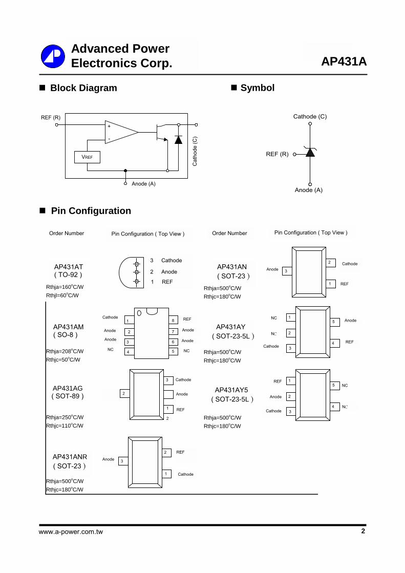
Advanced Power Electronics Corp. AP431A
Block Diagram REF (R)
VREF
+
-
Anode (A)
Cat
hode
(C)
Symbol
Pin Configuration
Order Number Pin Configuration ( Top View )
AP431AT ( TO-92 )
3 Cathode
2 Anode
1 REF
AP431AM ( SO-8 )
1
2
3
4
8
6
Anode
Anode
NC
Anode
Anode
NC
REF
Order Number Pin Configuration ( Top View )
AP431AN( SOT-23 )
Cathode
Anode
REF
AP431AY( SOT-23-5L )
NC Anode
3
2
1
12
5
4
1
3 REF
NC7
5
Cathode
Cathode
Cathode
NC
Anode 12
5
4
1
3
REF
NCCathode
AP431AY5( SOT-23-5L )
Anode
REF
2
3
1
Cathode
AP431AG( SOT-89 )
2
Cathode (C)
REF (R)
Anode (A)
AP431ANR( SOT-23 )
Anode
REF
3
2
1 Cathode
Rthja=160oC/W
Rthjl=60oC/W
Rthja=208oC/W
Rthjc=50oC/W
Rthja=250oC/W
Rthjc=110oC/W
Rthja=500oC/W
Rthjc=180oC/W
Rthja=500oC/W
Rthjc=180oC/W
Rthja=500oC/W
Rthjc=180oC/W
Rthja=500oC/W
Rthjc=180oC/W
josalul
Order Number Pin Configuration ( Top View ) AP431AT ( TO-92 ) 3 Cathode 2 Anode 1 REF AP431AM ( SOP-8 ) 1 2 3 4 8 6 Anode Anode NC Anode Anode NC REF Order Number Pin Configuration ( Top View ) AP431AN ( SOT-23 ) Cathode Anode REF AP431AY ( SOT-25 ) NC Anode 3 2 1 12 5 4 1 3 REF NC 7 5 Cathode Cathode Cathode NC Anode 12 5 4 1 3 REF NC Cathode AP431AY5 ( SOT-25 ) Anode REF 2 3 1 Cathode AP431AG ( SOP-89 ) 2 AP431ANR ( SOT-23 ) Anode REF 3 2 1 Cathode
josalul
josalul
josalul
josalul
josalul
josalul
josalul
josalul
josalul
josalul
www.a-power.com.tw
3
Advanced Power Electronics Corp.
AP431A
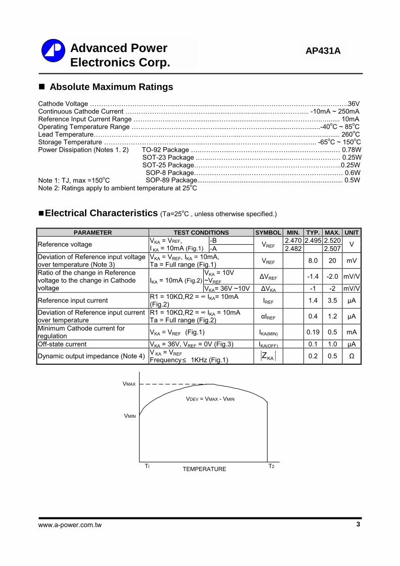
Absolute Maximum Ratings
Cathode Voltage ………………………………......….........................…...……………………………...……….36V Continuous Cathode Current ………………………….…….............…................…………….... -10mA ~ 250mA Reference Input Current Range ……………..………..............…….................................………….…....... 10mA Operating Temperature Range ………….…………..…….…….....………………...........………......-40oC ~ 85oC Lead Temperature………………………….………….…….…………....…………………….........…............ 260oC Storage Temperature ……………………………......…....….............………………..……...…....... -65oC ~ 150oC Power Dissipation (Notes 1. 2) TO-92 Package ….…………..………………………....………….....… 0.78W
SOT-23 Package .…...…………..…………….......…………………… 0.25W SOT-25 Package……………………...…………….………….………..0.25W SOP-8 Package……………….………………………………………… 0.6W
Note 1: TJ, max =150oC Note 2: Ratings apply to ambient temperature at 25oC Electrical Characteristics (Ta=25oC , unless otherwise specified.)
PARAMETER TEST CONDITIONS SYMBOL MIN. TYP. MAX. UNIT-B 2.470 2.495 2.520Reference voltage VKA = VREF,
I KA = 10mA (Fig.1) -A VREF 2.482 2.507 V
Deviation of Reference input voltage over temperature (Note 3)
VKA = VREF, IKA = 10mA, Ta = Full range (Fig.1) VREF 8.0 20 mV
VKA = 10V ~VREF ∆VREF -1.4 -2.0 mV/VRatio of the change in Reference
voltage to the change in Cathode voltage
IKA = 10mA (Fig.2)VKA= 36V ~10V ∆VKA -1 -2 mV/V
Reference input current R1 = 10KΩ,R2 = ∞ IKA= 10mA (Fig.2) IREF 1.4 3.5 µA
Deviation of Reference input current over temperature
R1 = 10KΩ,R2 = ∞ IKA = 10mA Ta = Full range (Fig.2) αIREF 0.4 1.2 µA
Minimum Cathode current for regulation VKA = VREF (Fig.1) IKA(MIN) 0.19 0.5 mA
Off-state current VKA = 36V, VREF = 0V (Fig.3) IKA(OFF) 0.1 1.0 µA
Dynamic output impedance (Note 4) V KA = VREF Frequency ≤ 1KHz (Fig.1) KAZ 0.2 0.5 Ω
VMAX
VMIN
TI T2TEMPERATURE
VDEV = VMAX - VMIN
SOP-89 Package............................................................................... 0.5W
www.a-power.com.tw
4
Advanced Power Electronics Corp.
AP431A
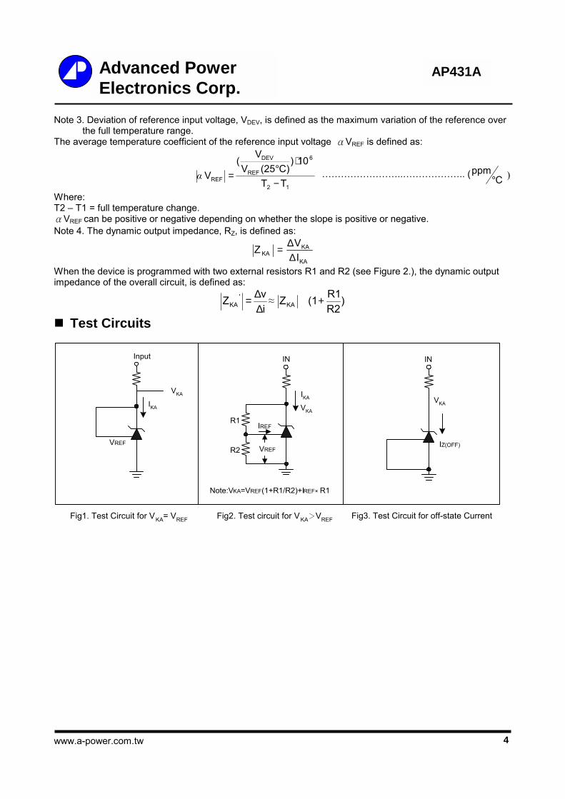
Note 3. Deviation of reference input voltage, VDEV, is defined as the maximum variation of the reference over the full temperature range.
The average temperature coefficient of the reference input voltage αVREF is defined as:
12
6
REF
DEV
REF TT
10)C)(25V
V(
V−
⋅°
=α ……………………..……………….. ( ) Cppm
°
Where: T2 – T1 = full temperature change. αVREF can be positive or negative depending on whether the slope is positive or negative. Note 4. The dynamic output impedance, RZ, is defined as:
KA
KAKA I
VZ∆∆
=
When the device is programmed with two external resistors R1 and R2 (see Figure 2.), the dynamic output impedance of the overall circuit, is defined as:
)R2R1(1Z
ivZ KA
'KA +
∆∆= ≈
Test Circuits
Input
VREF
VKA
IKA
Fig1. Test Circuit for VKA= VREF
IN
VREF
R1
R2
IREF
Note:VKA=VREF(1+R1/R2)+IREF× R1
IKA
VKA
Fig2. Test circuit for VKA>VREF
IN
VKA
IZ(OFF)
Fig3. Test Circuit for off-state Current
www.a-power.com.tw
5
Advanced Power Electronics Corp.
AP431A
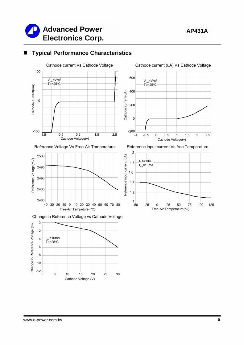
Typical Performance Characteristics
Cathode current Vs Cathode Voltage
-100
0
100
-1.5 -0.5 0.5 1.5 2.5Cathode Voltage(v)
Cat
hode
cur
rent
(mA
)
VKA=VrefTa=25oC
Cathode current (uA) Vs Cathode Voltage
-1Cathode Voltage(v)
Cat
hode
cur
rent
(uA
)
-200
200
400
600
0
-0.5 0 0.5 1 1.5 2 2.5
VKA=VrefTa=25oC
Reference Voltage Vs Free-Air Temperature
Free-Air Tempeture (oC)
Ref
eren
ce V
olta
ge(m
V)
2480
2485
2490
2495
2500
-40 80-30 -20 -10 0 10 20 30 40 50 60 70
Reference input current Vs free Temperature
Free-Air Temperature(oC)
Ref
eren
ce in
put c
urre
nt (u
A)
1
1.2
1.4
1.6
1.8
2
-50 -25 0 25 50 75 100 125
R1=10KIKA=10mA
Change in Reference Voltage vs Cathode Voltage
0 5 10 15 20 25 30Cathode Voltage (V)
Cha
nge
in R
efer
ence
Vol
tage
(mv)
-12
-10
-8
-6
-4
-2
0
IKA=10mATa=25oC
www.a-power.com.tw
6
Advanced Power Electronics Corp.
AP431A
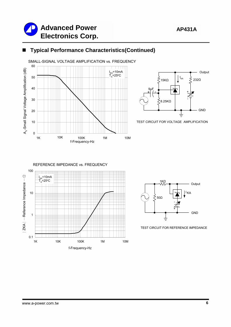
Typical Performance Characteristics(Continued)
+ - +
-
Output
GND
15KΩ
8.25KΩ
9µF
IKA 232Ω
TEST CIRCUIT FOR VOLTAGE AMPLIFICATION
SMALL-SIGNAL VOLTAGE AMPLIFICATION vs. FREQUENCY
0
10
20
30
40
50
60
1K 10K 100K 1M 10Mf-Frequency-Hz
AV-
Sm
all S
igna
l Vol
tage
Am
plifi
catio
n (d
B)
IKA=10mATA=25oC
+
-
I KA
GND
Output1KΩ
50Ω
TEST CIRCUIT FOR REFERENCE IMPEDANCE
REFERENCE IMPEDANCE vs. FREQUENCY
0.1
1
10
100
1K 10K 100K 1M 10M
f-Frequency-Hz
∣ZK
A∣—
Ref
eren
ce Im
peda
nce—Ω IKA=10mA
TA=25oC
www.a-power.com.tw
7
Advanced Power Electronics Corp.
AP431A
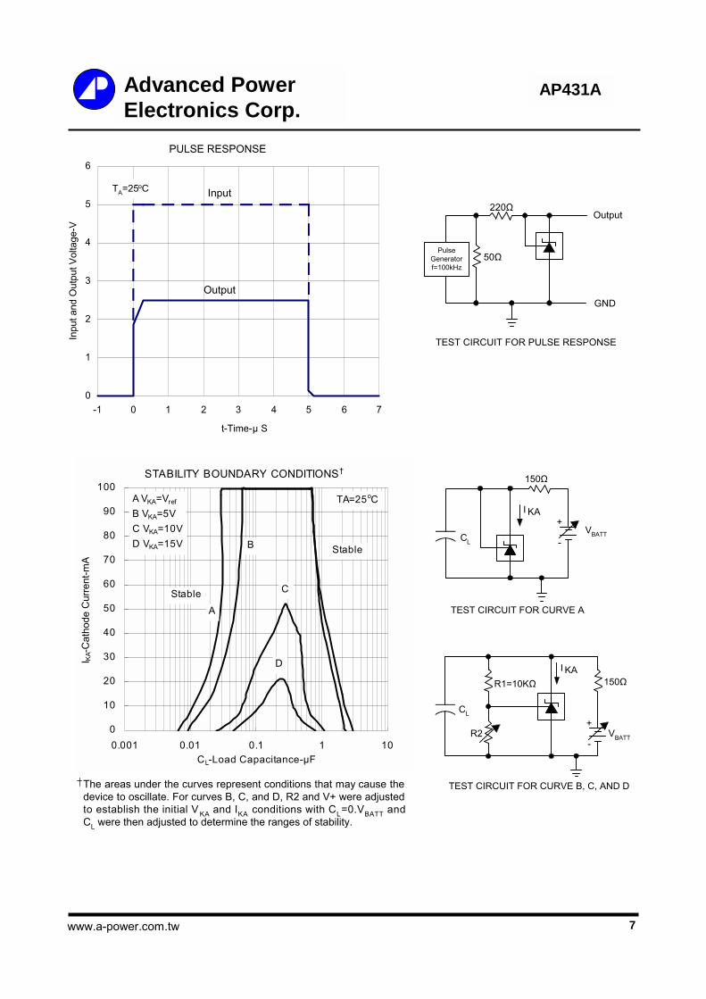
PULSE RESPONSE
0
1
2
3
4
5
6
-1 0 1 2 3 4 5 6 7
t-Time-µ S
Inpu
t and
Out
put V
olta
ge-V
Input
OutputGND
Output220Ω
50Ω
TEST CIRCUIT FOR PULSE RESPONSE
PulseGeneratorf=100kHz
TA=25oC
+
-
150Ω
I KA
VBATTCL
TEST CIRCUIT FOR CURVE A
+
-
CL
R1=10KΩ
R2
I KA150Ω
VBATT
TEST CIRCUIT FOR CURVE B, C, AND DThe areas under the curves represent conditions that may cause thedevice to oscillate. For curves B, C, and D, R2 and V+ were adjustedto establish the initial V KA and IKA conditions with CL=0.VBATT andCL were then adjusted to determine the ranges of stability.
STABILITY BOUNDARY CONDITIONS†
0
10
20
30
40
50
60
70
80
90
100
0.001 0.01 0.1 1 10CL-Load Capacitance-µF
I KA-
Cat
hode
Cur
rent
-mA
A VKA=Vref
B VKA=5VC VKA=10VD VKA=15V
A
B
C
D
Stable
Stable
TA=25oC
www.a-power.com.tw
8
Advanced Power Electronics Corp.
AP431A
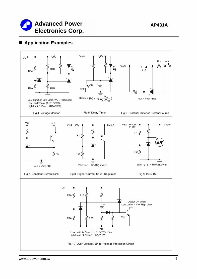
Application Examples
VIN
+
Low Limit VREF(1 + R1B/R2B) +VBEHigh Limit VREF(1 + R1A/R2A)
R1A R1B
R2A R2B VBE
Output ON whenLow Limint < VIN< High Limit
Fig.10 Over-Voltage / Under-Voltage Protection Circuit
VIN
RCL IOUT
IOUT = VREF / RCL
Fig.6 Current Limiter or Current Source
IOUTVIN
IOUT = VREF / RS
RS
Fig.7 Constant-Current Sink
Fig.4 Voltage Monitor Fig.5 Delay Timer
VOUT = (1 + R1/R2) x VREF
VIN
R1
R2
Fig.8 Higher-Current Shunt Regulator
VOUT VINPUSE
R1
R2
LIMIT (1 + R1/R2) x VREF
Fig.9 Crow Bar
VOUT
VIN
ONOFF
R
+
VINDelay = RC x ln( VIN -VREF)LED on when Low Limit<VIN<High Limit
Low Limit ≈ VREF (1+R1B/R2B)High Limit ≈ VREF (1+R1A/R2A)
R1A
R2A
VIN
R1B
R2B
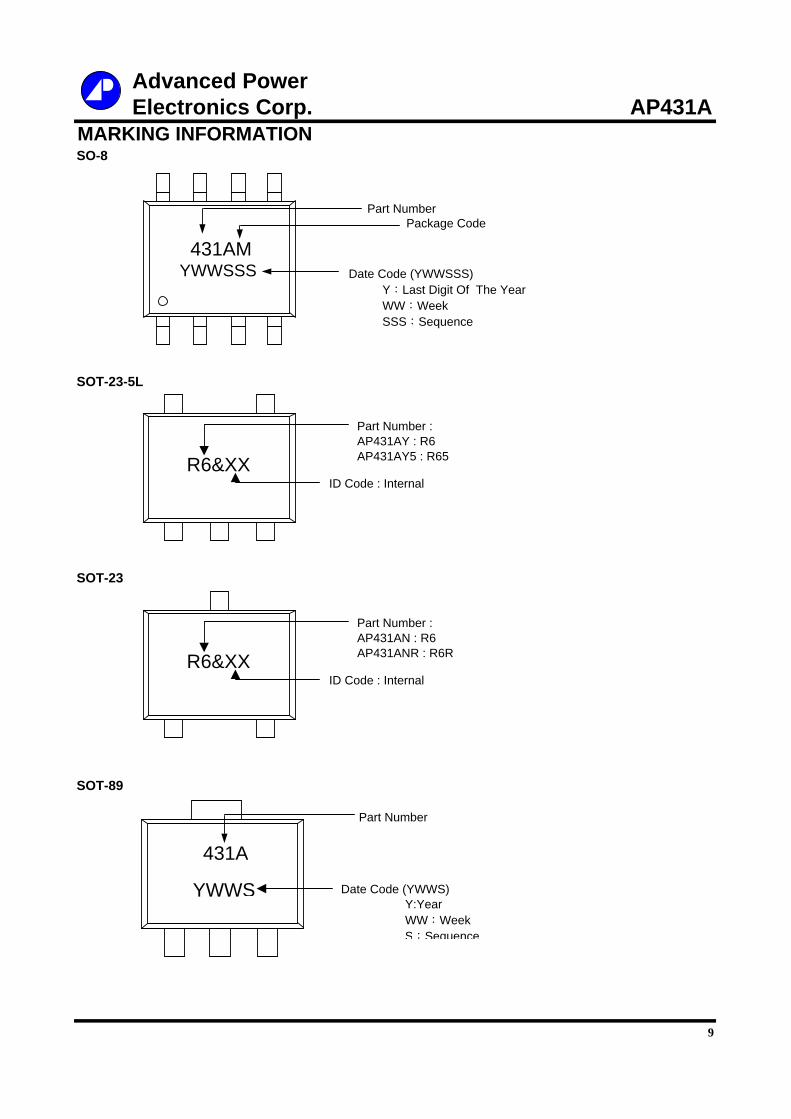
Advanced Power Electronics Corp. AP431AMARKING INFORMATIONSO-8
SOT-23-5L
SOT-23
SOT-89
9
431AMYWWSSS
Part Number
Date Code (YWWSSS) Y:Last Digit Of The Year WW:Week SSS:Sequence
Package Code
R6&XX
Part Number :AP431AY : R6AP431AY5 : R65
ID Code : Internal
R6&XX
Part Number :AP431AN : R6AP431ANR : R6R
ID Code : Internal
431A
Part Number
YWWS Date Code (YWWS) Y:Year WW:Week
S:Sequence
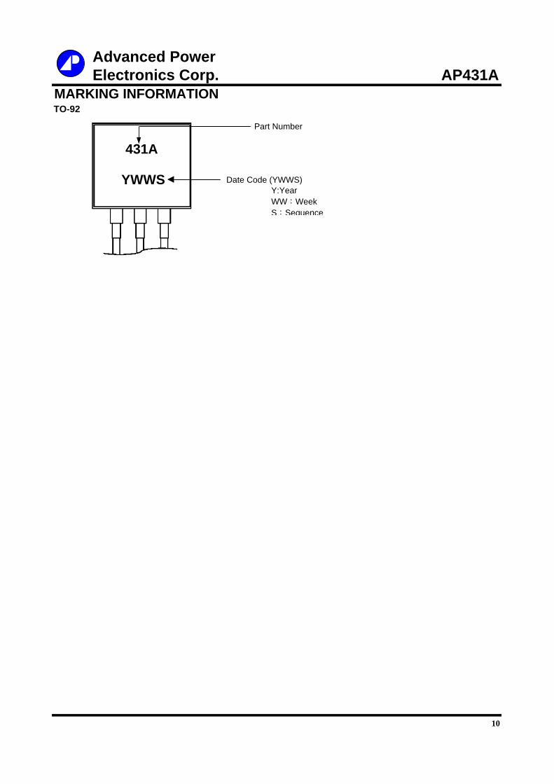
Advanced Power Electronics Corp. AP431AMARKING INFORMATIONTO-92
10
431A
YWWS
Part Number
Date Code (YWWS) Y:Year WW:Week
S:Sequence