Advanced Power Electronics Corp. APE8937 ULTRA - … OAD S ED TU a-low R ON lo ntains one ver an inp...
14
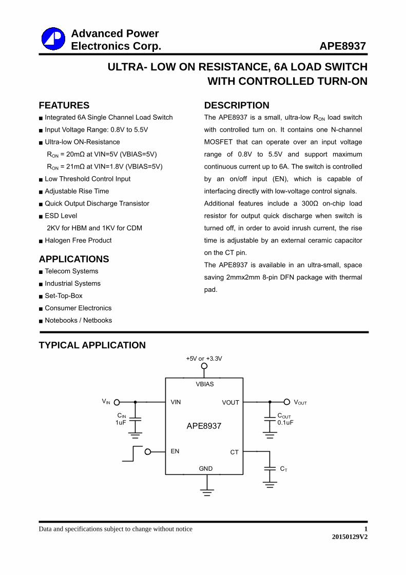
Data and spe A E FEATUR ▓ Integrated ▓ Input Volt ▓ Ultra-low R ON = 20 R ON = 21 ▓ Low Thre ▓ Adjustable ▓ Quick Ou ▓ ESD Leve 2KV for H ▓ Halogen F APPLIC ▓ Telecom S ▓ Industrial ▓ Set-Top-B ▓ Consume ▓ Notebook TYPICA ecifications su Advanc Electron U RES d 6A Single C age Range: ON-Resistan 0mΩ at VIN=5 mΩ at VIN= shold Contro e Rise Time tput Discharg el HBM and 1K Free Product ATIONS Systems Systems Box er Electronics ks / Netbooks AL APPLI V IN ubject to chang ced Pow nics Co ULTRA- Channel Loa 0.8V to 5.5V nce 5V (VBIAS=5 1.8V (VBIAS ol Input ge Transisto KV for CDM t s s CATION CIN 1uF ge without not wer orp. - LOW O d Switch V 5V) S=5V) r VIN EN tice ON RES WI DES The A with c MOS range contin by a interfa Addit resist turned time i on the The A savin pad. GND APE8937 VBIAS +5V or +3.3V SISTANC TH CON SCRIPTIO APE8937 is controlled tu FET that ca e of 0.8V nuous curren an on/off in acing directly ional feature tor for outpu d off, in orde is adjustable e CT pin. APE8937 is g 2mmx2mm 7 VOUT CT V CE, 6A L NTROLL ON a small, ultr urn on. It co an operate o to 5.5V an nt up to 6A. T nput (EN), y with low-vo es include ut quick disc er to avoid i e by an exte available in m 8-pin DFN C OUT 0.1uF C T AP LOAD S LED TU ra-low R ON lo ontains one over an inp nd support The switch is which is c oltage contro a 300Ω on charge when nrush curren ernal ceramic an ultra-sm N package w VOUT 1 20150129V2 PE8937 SWITCH URN-ON oad switch N-channel put voltage maximum s controlled capable of l signals. -chip load n switch is nt, the rise c capacitor mall, space ith thermal 1 2
Transcript of Advanced Power Electronics Corp. APE8937 ULTRA - … OAD S ED TU a-low R ON lo ntains one ver an inp...
Data and spe
AE
FEATUR Integrated
Input Volt
Ultra-low
RON = 20
RON = 21
Low Thre
Adjustable
Quick Ou
ESD Leve
2KV for H
Halogen F
APPLIC Telecom S
Industrial
Set-Top-B
Consume
Notebook
TYPICA
ecifications su
AdvancElectron
U
RES d 6A Single C
age Range:
ON-Resistan
0mΩ at VIN=5
mΩ at VIN=
shold Contro
e Rise Time
tput Discharg
el
HBM and 1K
Free Product
ATIONS Systems
Systems
Box
er Electronics
ks / Netbooks
AL APPLI
VIN
ubject to chang
ced Pownics Co
ULTRA-
Channel Loa
0.8V to 5.5V
nce
5V (VBIAS=5
1.8V (VBIAS
ol Input
ge Transisto
KV for CDM
t
s
s
CATION
CIN1uF
ge without not
wer orp.
- LOW O
d Switch
V
5V)
S=5V)
r
VIN
EN
tice
ON RESWI
DESThe A
with c
MOS
range
contin
by a
interfa
Addit
resist
turned
time i
on the
The A
savin
pad.
GND
APE8937
VBIAS
+5V or +3.3V
SISTANCTH CON
SCRIPTIOAPE8937 is
controlled tu
FET that ca
e of 0.8V
nuous curren
an on/off in
acing directly
ional feature
tor for outpu
d off, in orde
is adjustable
e CT pin.
APE8937 is
g 2mmx2mm
7
VOUT
CT
V
CE, 6A LNTROLL
ON a small, ultr
urn on. It co
an operate o
to 5.5V an
nt up to 6A. T
nput (EN),
y with low-vo
es include
ut quick disc
er to avoid i
e by an exte
available in
m 8-pin DFN
COUT0.1uF
CT
AP
LOAD SLED TU
ra-low RON lo
ontains one
over an inp
nd support
The switch is
which is c
oltage contro
a 300Ω on
charge when
nrush curren
ernal ceramic
an ultra-sm
N package w
VOUT
120150129V2
PE8937
SWITCHURN-ON
oad switch
N-channel
put voltage
maximum
s controlled
capable of
l signals.
-chip load
n switch is
nt, the rise
c capacitor
mall, space
ith thermal
1 2
AE
ORDER
APE8937
ABSOLUVIN
VOUT
EN, CT
VBIAS
IMAX
Storage Te
Junction Te
Lead Temp
Thermal Re
DFN
Electrostati
HB
CD
RECOMVIN
VBIAS
VOUT
CIN
Junction Te
Operating T
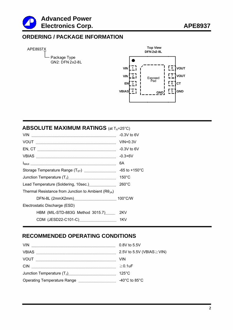
AdvancElectronING / PA
PackagGN2: D
7X
UTE MAX
mperature R
emperature (
perature (Sol
esistance fro
N-8L (2mmX
c Discharge
M (MIL-STD
M (JESD22-
MMENDED
emperature (
Temperature
ced Pownics Co
ACKAGE
ge TypeDFN 2x2-8L
XIMUM R
Range (TST)
TJ)
dering, 10se
m Junction t
X2mm)
(ESD)
D-883G Meth
-C101-C)
D OPERA
TJ)
e Range
wer orp.
INFORM
RATINGS
ec.)
to Ambient (R
hod 3015.7)
ATING C
MATION
VIN
VIN
E
VBIA
S (at TA=25°C -0.3V
VIN+
-0.3V
-0.3
6A
-65 t
150°
260°
RθJA)
100°C
2KV
1KV
CONDITIO 0.8V
2.5V
VIN
≧0.
125°
-40°
DFT
1
2
3
4
N
N
EN
AS
C) V to 6V
+0.3V
V to 6V
+6V
to +150°C
°C
°C
C/W
V
V
ONS V to 5.5V
V to 5.5V (VB
1uF
°C
C to 85°C
FN 2x2-8LTop View
Exposed Pad
GND
BIAS≧VIN)
AP
5
6
7
8
GND
CT
VOUT
VOUT
2
PE8937
2

AE
ELECTR(VIN=0.8 to
PAR
Quiescent C
Shutdown C
ON Resista
Output Pull
EN Input Le
EN Thresho
Note1: Gua
Note2: Mak
AdvancElectronRICAL SP 5.5V, VBIAS
RAMETER
Current
Current
nce
Down Resis
eakage Curre
old
rantee by de
ke sure VBAIS
ced Pownics CoPECIFICAS=5V,CIN=1u
SYM
IBIAS
ISD
RON
stance ROP
ent ION
VEN
VEN
esign, not pro
≧VIN for opt
wer orp. ATIONSF, COUT=0.1u
M
S VBIAS=VIN
VBIAS=VIN
VEN=GND
N
VIN=5V, I
VIN=5V, I
-40oC < T
VIN=2.5V
VIN=2.5V
85oC
VIN=1.8V
VIN=1.8V
85oC
VIN=1.5V
VIN=1.5V
85oC
VIN=1.05
VIN=1.05
< 85oC
VIN=0.8V
VIN=0.8V
85oC
D VBIAS=5V,
VEN=5V o
H on
L off
oduction test
imum RON pe
uF, TA =25°C
TEST CON
=VEN=5V, IOU
=VEN=2.5V, I
D
IOUT=-200m
IOUT=-200m
TA < 85oC
V, IOUT=-200
V, IOUT=-200
V, IOUT=-200
V, IOUT=-200
V, IOUT=-200
V, IOUT=-200
5V, IOUT=-20
5V, IOUT=-20
V, IOUT=-200
V, IOUT=-200
VEN=0V
or GND
ted.
erformance.
C, unless othe
NDITION
UT=0A
IOUT=0A
mA
mA,
0mA
0mA, -40oC <
0mA
0mA, -40oC <
0mA
0mA, -40oC <
00mA
00mA, -40oC
0mA
0mA, -40oC <
erwise speci
MIN
< TA <
< TA <
< TA <
C < TA
< TA <
1.2
AP
fied)
N TYP M
50
30
20
20
20
20
20
20
300
3
PE8937
MAX UNIT
75 uA
50 uA
1 uA
26 mΩ
33 mΩ
26 mΩ
33 mΩ
26 mΩ
33 mΩ
26 mΩ
33 mΩ
26 mΩ
33 mΩ
26 mΩ
33 mΩ
350 Ω
1 uA
V
0.5 V
3
AE
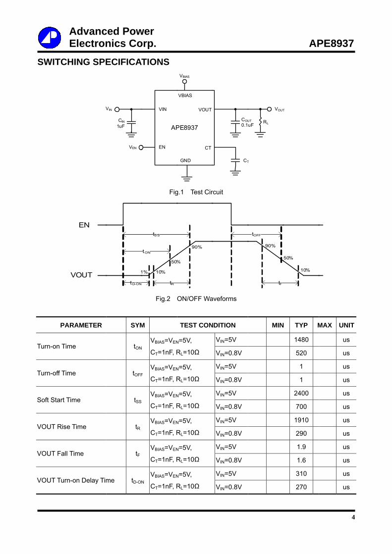
SWITCH
V
PAR
Turn-on Tim
Turn-off Tim
Soft Start Ti
VOUT Rise
VOUT Fall T
VOUT Turn-
AdvancElectronHING SPE
V
EN
VOUT
RAMETER
me
me
ime
Time
Time
-on Delay Tim
ced Pownics CoECIFICAT
CIN1uF
VIN
VEN
1
tD-ON
SYM
tON
tOFF
tSS
tR
tF
me tD-ON
wer orp. ATIONS
VIN
AP
EN
Fig
tON
tR
10%
50%
tSS
1%
Fig.2
M
VBIAS=VEN
CT=1nF, R
F VBIAS=VEN
CT=1nF, R
VBIAS=VEN
CT=1nF, R
VBIAS=VEN
CT=1nF, R
VBIAS=VEN
CT=1nF, R
N VBIAS=VEN
CT=1nF, R
GND
PE8937
VOUT
CT
VBIAS
VBIAS
g.1 Test Cir
90%
%
ON/OFF Wa
TEST CON
N=5V,
RL=10Ω
N=5V,
RL=10Ω
N=5V,
RL=10Ω
N=5V,
RL=10Ω
N=5V,
RL=10Ω
N=5V,
RL=10Ω
COU0.1
CT
rcuit
aveforms
NDITION
VIN=5V
VIN=0.8V
VIN=5V
VIN=0.8V
VIN=5V
VIN=0.8V
VIN=5V
VIN=0.8V
VIN=5V
VIN=0.8V
VIN=5V
VIN=0.8V
UTuF
VOUT
T
RL
tF
90%
tOFF
MIN
AP
T
10%
50%
N TYP M
1480
520
1
1
2400
700
1910
290
1.9
1.6
310
270
4
PE8937
MAX UNIT
us
us
us
us
us
us
us
us
us
us
us
us
4
AE
PIN DES
PIN No.
1, 2
3
4
5
6
7, 8
Exposed
pad
BLOCK
EN
VBIAS
AdvancElectronSCRIPTIO
PIN S
V
E
VB
G
C
VO
d G
DIAGRA
Os
Char
ced Pownics CoONS
YMBOL
VIN I
EN E
BIAS B
GND G
CT A
OUT S
GND T
AM
scillator
rge Pump
wer orp.
Input power
Enable contr
Bias voltage
Ground.
A capacitor t
Switch outpu
Tie to ground
ContLogi
CT
supply; bypa
rol input, acti
.
to ground set
ut
d to alleviate
rolic
T
PIN DESC
ass this input
ive high. Do
t the rise tim
e thermal stre
Output D
CRIPTION
t with a ceram
not leave flo
e of VOUT.
ess.
ischarge
AP
mic capacito
oating.
5
PE8937
or to ground.
VIN
VOUT
GND
5
AE
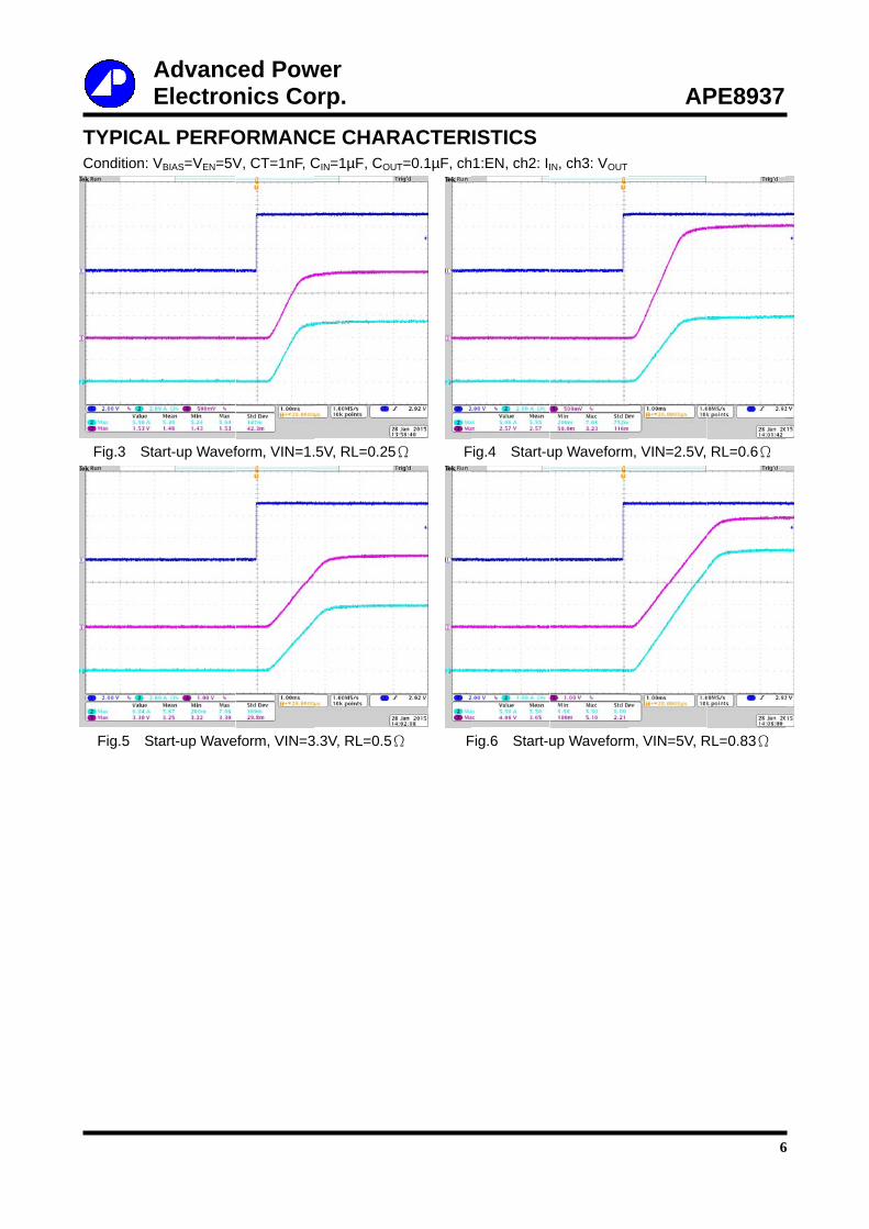
TYPICACondition: V
Fig.3 Sta
Fig.5 St
AdvancElectron
AL PERFOVBIAS=VEN=5V
art-up Wavef
tart-up Wave
ced Pownics CoORMANCV, CT=1nF, C
form, VIN=1.
eform, VIN=3
wer orp. CE CHARCIN=1µF, COU
.5V, RL=0.25
3.3V, RL=0.5
RACTERUT=0.1µF, ch
5Ω F
Ω F
ISTICS1:EN, ch2: II
Fig.4 Start-u
Fig.6 Start-u
IN, ch3: VOUT
up Waveform
up Waveform
AP
m, VIN=2.5V,
m, VIN=5V, R
6
PE8937
RL=0.6Ω
RL=0.83Ω
6
AE
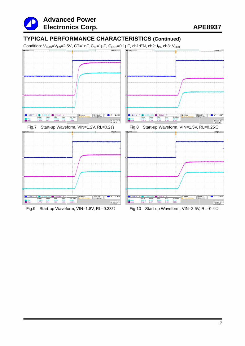
TYPICACondition: V
Fig.7 St
Fig.9 Sta
AdvancElectron
AL PERFOVBIAS=VEN=2.
tart-up Wave
art-up Wavef
ced Pownics CoORMANC5V, CT=1nF
eform, VIN=1
form, VIN=1.
wer orp. CE CHARF, CIN=1µF, C
.2V, RL=0.2
.8V, RL=0.33
RACTERCOUT=0.1µF, c
Ω Fi
3Ω Fi
ISTICS (Cch1:EN, ch2
g.8 Start-u
g.10 Start-
Continued: IIN, ch3: VOU
p Waveform
-up Waveform
APd) UT
, VIN=1.5V,
m, VIN=2.5V
7
PE8937
RL=0.25Ω
V, RL=0.4Ω
7
AE
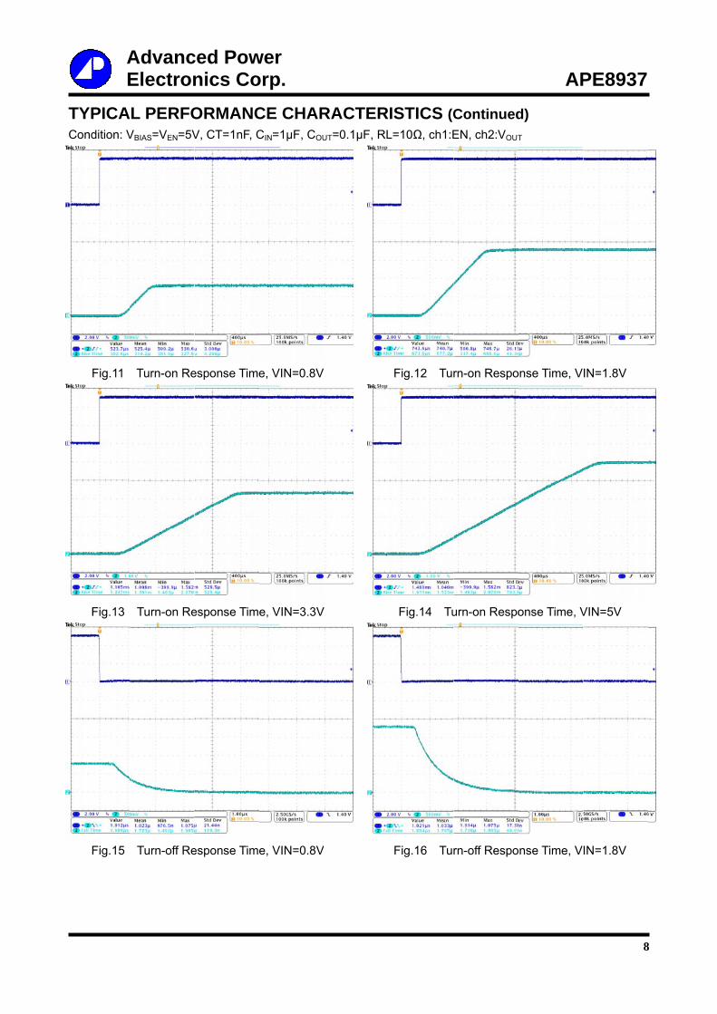
TYPICACondition: V
Fig.11
Fig.13
Fig.15
AdvancElectron
AL PERFOVBIAS=VEN=5V
Turn-on Re
Turn-on Re
Turn-off Re
ced Pownics CoORMANCV, CT=1nF, C
esponse Time
esponse Tim
esponse Tim
wer orp. CE CHARCIN=1µF, COU
e, VIN=0.8V
e, VIN=3.3V
e, VIN=0.8V
RACTERUT=0.1µF, RL
V
V
ISTICS (CL=10Ω, ch1:E
Fig.12 Tur
Fig.14 Tu
Fig.16 Tur
ContinuedEN, ch2:VOUT
rn-on Respo
urn-on Respo
rn-off Respo
APd) T
onse Time, V
onse Time, V
onse Time, V
8
PE8937
IN=1.8V
VIN=5V
IN=1.8V
8

AE
TYPICACondition: V
Fig.17
Fig.1
Fig.2
AdvancElectron
AL PERFOVBIAS=VEN=5V
Turn-off Re
9 Turn-on
1 Turn-on
ced Pownics CoORMANCV, CT=1nF, C
esponse Tim
Delay Time,
Delay Time,
wer orp. CE CHARCIN=1µF, COU
e, VIN=3.3V
VIN=0.8V
VIN=3.3V
RACTERUT=0.1µF, RL
V
ISTICS (CL=10Ω, ch1:E
Fig.18 Tu
Fig.20 T
Fig.22
ContinuedEN, ch2:VOUT
urn-off Respo
Turn-on Dela
Turn-on Del
APd) T
onse Time, V
ay Time, VIN
ay Time, VIN
9
PE8937
VIN=5V
=1.8V
N=5V
9
AE
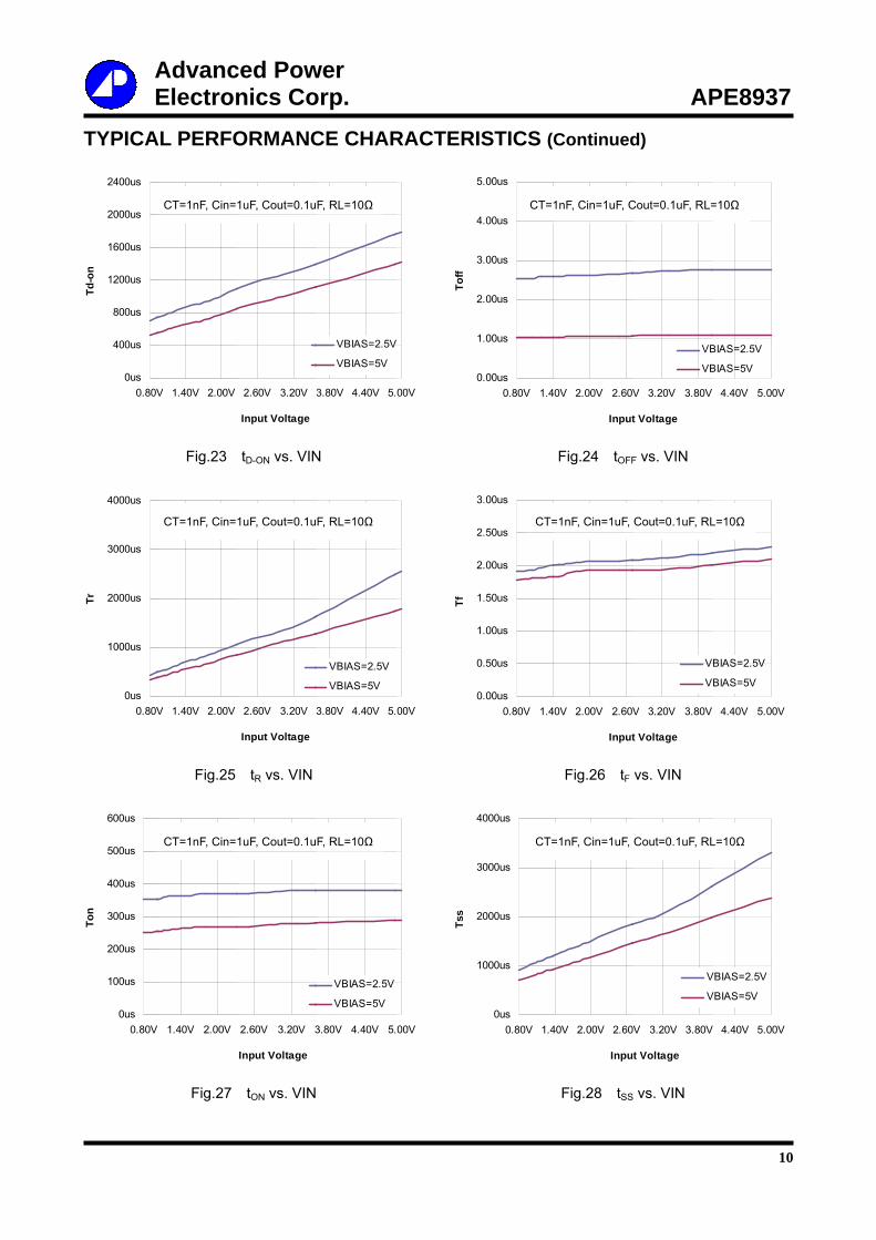
TYPICA
0us
400us
800us
1200us
1600us
2000us
2400us
0.80V
Td-o
n
0us
1000us
2000us
3000us
4000us
0.80V
Tr
0us
100us
200us
300us
400us
500us
600us
0.80V
Ton
AdvancElectron
AL PERFO
Fig.23
Fig.25
Fig.27
V 1.40V 2.00V
V 1.40V 2.00V
1.40V 2.00V
CT=1nF, Cin=1
CT=1nF, Cin=1
CT=1nF, Cin=1
ced Pownics CoORMANC
tD-ON vs. VIN
tR vs. VIN
tON vs. VIN
2.60V 3.20V 3
Input Voltage
2.60V 3.20V 3
Input Voltage
2.60V 3.20V 3
Input Voltage
1uF, Cout=0.1u
1uF, Cout=0.1u
1uF, Cout=0.1u
wer orp. CE CHAR
N
3.80V 4.40V 5.
VBIAS=2.5V
VBIAS=5V
3.80V 4.40V 5.
VBIAS=2.5V
VBIAS=5V
3.80V 4.40V 5.
VBIAS=2.5V
VBIAS=5V
F, RL=10Ω
F, RL=10Ω
F, RL=10Ω
RACTER
00V
V
Toff
00V
Tf
00V
Tss
ISTICS (C
0.00us
1.00us
2.00us
3.00us
4.00us
5.00us
0.80V 1.4
0.00us
0.50us
1.00us
1.50us
2.00us
2.50us
3.00us
0.80V 1.4
0us
1000us
2000us
3000us
4000us
0.80V 1.4
CT=1
CT=
CT=
Continued
Fig.24 tOFF
Fig.26 tF
Fig.28 tSS
0V 2.00V 2.60V
Input
0V 2.00V 2.60V
Input
40V 2.00V 2.60V
Input
1nF, Cin=1uF, C
=1nF, Cin=1uF,
=1nF, Cin=1uF,
APd)
F vs. VIN
vs. VIN
vs. VIN
V 3.20V 3.80V
t Voltage
VB
VB
V 3.20V 3.80V
t Voltage
V
V
V 3.20V 3.80V
t Voltage
V
V
Cout=0.1uF, RL=
Cout=0.1uF, RL
Cout=0.1uF, RL
10
PE8937
4.40V 5.00V
BIAS=2.5V
BIAS=5V
4.40V 5.00V
BIAS=2.5V
BIAS=5V
V 4.40V 5.00V
VBIAS=2.5V
VBIAS=5V
=10Ω
L=10Ω
L=10Ω
0

AE
TYPICA
Fig.31
Fig
10mΩ
15mΩ
20mΩ
25mΩ
30mΩ
35mΩ
-50
Ron
0
10
20
30
40
50
60
70
-40
I BIA
S(u
A)
0.0uA
0.2uA
0.4uA
0.6uA
0.8uA
1.0uA
0.8V
I SD
AdvancElectron
AL PERFO
Fig.29 RON
Quiescent
g.33 Shutdo
0
-20 0 20
V 1.8V
ced Pownics CoORMANC
N vs. Tempera
Current vs. T
own Current
50
Temperature
0 40 60
TJ (°C)
VBIA
VBIA
2.8V 3.8VInput Voltage
wer orp. CE CHAR
ature
Temperature
vs. VIN
100
VBIAS=2
VBIAS=5
80 100 120
AS=VIN=5V
AS=VIN=3.3V
V 4.8Ve
VBIAS=5V
VBIAS=2.5V
RACTER
150
.5V
5V
1
1
2
2
3
3
4
Ron
0
VE
N(V
)
5.8V
V
ISTICS (C
Fig.32 E
10mΩ
15mΩ
20mΩ
25mΩ
30mΩ
35mΩ
40mΩ
0.80V 1
0.0
0.2
0.4
0.6
0.8
1.0
1.2
1.4
1.6
1.8
2.0
-40 -20
VE
N(V
)
Continued
Fig.30 RON
EN Threshold
1.80V 2.80V
Inpu
0 0 20 4
T
APd)
N vs. VIN
d vs. Tempe
3.80V
ut Voltage
40 60 80
TJ (°C)
11
PE8937
rature
4.80V 5.80V
VBIAS=2.5V
VBIAS=5V
100 120
VEN-H
VEN-L
1
V

AE
APPLICOn/Off ConThe load sw
capable of i
GPIO logic
Output RisThe rise tim
Table 1 are
VIN
0nF
0.22nF
0.47nF
1nF
2.2nF
4.7nF
10nF
Input CapaAn input ca
supply durin
Output CapSetting a C
switch, this
removed.
AdvancElectronATION IN
ntrol witch is cont
nterfacing w
threshold. D
e Time Conme of VOUT
typical meas
VIN=0.8V
22
76
136
262
602
1246
2587
acitor pacitor is rec
ng high curre
pacitor CIN greater th
prevents the
ced Pownics CoNFORMA
trolled by the
ith low voltag
Do not leave t
trol is adjustable
sured value.
Rise T
VIN=1.05V
26
98
174
347
753
1638
3411
commended
ent applicatio
han the COUT
e current flow
wer orp. ATION
e EN pin. Th
ge signals. T
the EN pin flo
e by an exte
Please refer
Time,TR(u
VIN=1.2V
30
115
209
412
902
1832
3865
to be placed
on.
T is highly re
ws through th
he EN pin is
The EN pin ca
oat.
ernal capacit
r it for determ
us),10%~90
T
VIN=1.5V
35
143
261
515
1136
2312
4908
<Table 1>
d between V
ecommended
he body diod
s active high
an be used w
or on the CT
mined rise tim
0%,COUT=
TR
VIN=1.8V
38
167
304
614
1348
2742
5712
IN and GND
d. Since the
de from VOU
h and has a
with standard
T pin. The ris
me.
=0.1uF,CIN
VIN=2.5V
46
232
428
847
1835
3906
8209
to limit the v
internal bod
UT to VIN wh
AP
low thresho
d 1.2V, 1.8V, 2
se time show
N=1uF
VIN=3.3V
55
301
559
1111
2493
5146
10860
voltage drop
dy diode is in
hen the syste
12
PE8937
old making it
2.5V or 3.3V
ws on below
VIN=5.0V
75
462
859
1712
3884
8084
17150
on the input
n the NMOS
em supply is
2
t
V
w
t
S
s
AE
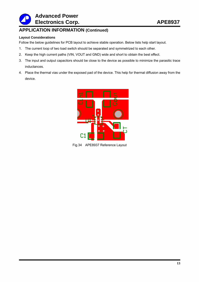
APPLICLayout ConFollow the b
1. The cur
2. Keep th
3. The inp
inducta
4. Place th
device.
AdvancElectronATION INnsiderationsbelow guidel
rrent loop of
he high curre
put and outpu
nces.
he thermal vi
ced Pownics CoNFORMAs ines for PCB
two load swi
ent paths (VIN
ut capacitors
ias under the
wer orp. ATION (C
B layout to ac
itch should b
N, VOUT and
s should be c
e exposed pa
Fig.34 APE
ontinued)
chieve stable
be separated
d GND) wide
close to the d
ad of the dev
E8937 Refer
)
e operation. B
and symme
e and short to
device as po
vice. This hel
rence Layout
Below lists h
etrized to eac
o obtain the
ossible to min
lp for therma
t
AP
elp start layo
ch other.
best effect.
nimize the pa
al diffusion aw
13
PE8937
out.
arasitic trace
way from the
3
e
e

AE
MARKINDFN 2x2-8L
8
Y
AdvancElectronNG INFOL
8937
YWWS
ced Pownics CoRMATIO
wer orp.
N
Part Numb
Date CodeY : YearWW : WeeS : Seque
ber
e (YWWS)
eknce
AP
14
PE8937
4