A DC-100 GHz Bandwidth and 20.5 dB Gain · CSICS 2013 Monterey, California A DC-100 GHz Bandwidth...
18
CSICS 2013 Monterey, California A DC-100 GHz Bandwidth and 20.5 dB Gain Limiting Amplifier in 0.25μm InP DHBT Technology Saeid Daneshgar, Prof. Mark Rodwell (UCSB) Zach Griffith (Teledyne Scientific Company)
Transcript of A DC-100 GHz Bandwidth and 20.5 dB Gain · CSICS 2013 Monterey, California A DC-100 GHz Bandwidth...
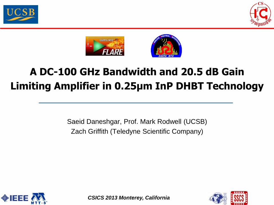
CSICS 2013 Monterey, California
A DC-100 GHz Bandwidth and 20.5 dB Gain
Limiting Amplifier in 0.25μm InP DHBT Technology
Saeid Daneshgar, Prof. Mark Rodwell (UCSB)
Zach Griffith (Teledyne Scientific Company)
CSICS 2013 Monterey, California
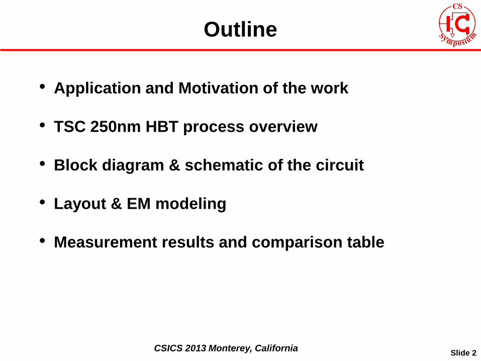
Outline
Slide 2
• Application and Motivation of the work
• TSC 250nm HBT process overview
• Block diagram & schematic of the circuit
• Layout & EM modeling
• Measurement results and comparison table
CSICS 2013 Monterey, California
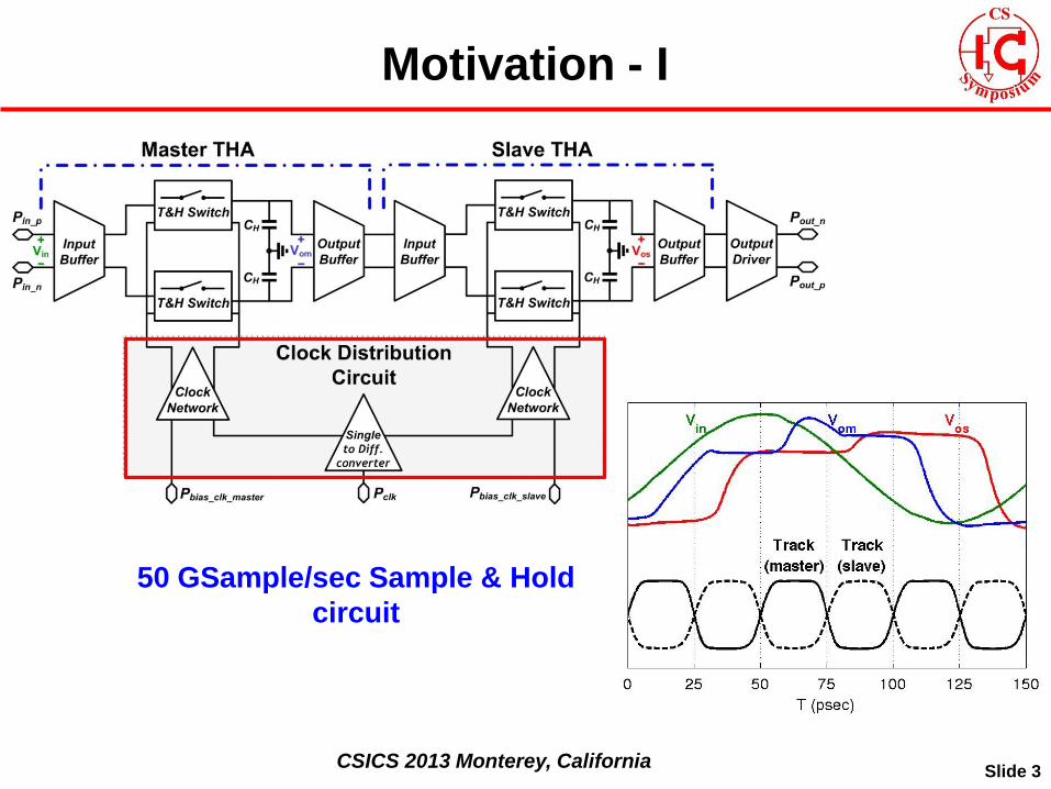
Motivation - I
Slide 3
50 GSample/sec Sample & Hold
circuit
CSICS 2013 Monterey, California
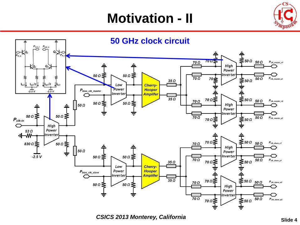
Motivation - II
Slide 4
50 GHz clock circuit
CSICS 2013 Monterey, California
Applications - I
Slide 5
• High speed optoelectronic signal conversion
requires broadband receivers
• Limiting amplifiers are the key components in
these receivers in order to:
Provide a low input sensitivity and sufficient gain to achieve
saturated output levels from small-signal inputs which
enables reliable decision making
Provide a wide bandwidth to achieve short rise and fall times
in order to provide an output signal with minimum distortion
CSICS 2013 Monterey, California
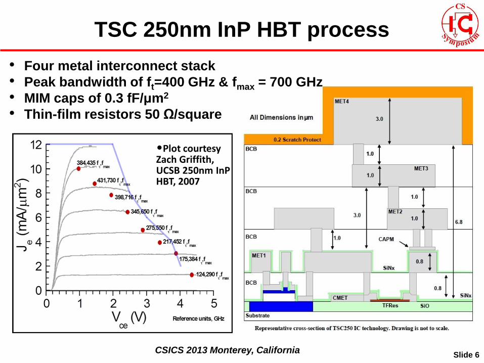
TSC 250nm InP HBT process
Slide 6
• Four metal interconnect stack
• Peak bandwidth of ft=400 GHz & fmax = 700 GHz
• MIM caps of 0.3 fF/μm2
• Thin-film resistors 50 Ω/square
•Plot courtesy Zach Griffith, UCSB 250nm InP HBT, 2007
CSICS 2013 Monterey, California
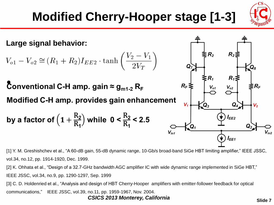
Modified Cherry-Hooper stage [1-3]
Slide 7
[1] Y. M. Greshishchev et al., “A 60-dB gain, 55-dB dynamic range, 10-Gb/s broad-band SiGe HBT limiting amplifier,” IEEE JSSC,
vol.34, no.12, pp. 1914-1920, Dec. 1999.
[2] K. Ohhata et al., “Design of a 32.7-GHz bandwidth AGC amplifier IC with wide dynamic range implemented in SiGe HBT,”
IEEE JSSC, vol.34, no.9, pp. 1290-1297, Sep. 1999
[3] C. D. Holdenried et al., “Analysis and design of HBT Cherry-Hooper amplifiers with emitter-follower feedback for optical
communications,” IEEE JSSC, vol.39, no.11, pp. 1959-1967, Nov. 2004.
Large signal behavior:
•
CSICS 2013 Monterey, California
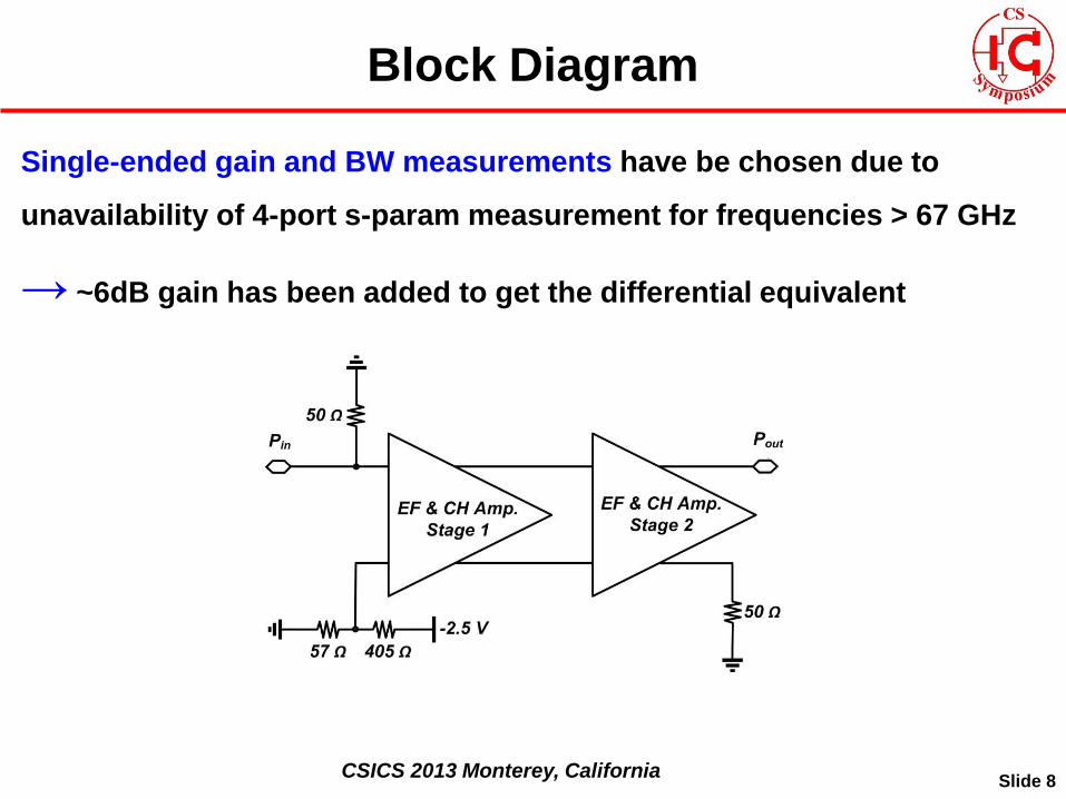
Block Diagram
Slide 8
Single-ended gain and BW measurements have be chosen due to
unavailability of 4-port s-param measurement for frequencies > 67 GHz
→ ~6dB gain has been added to get the differential equivalent
CSICS 2013 Monterey, California
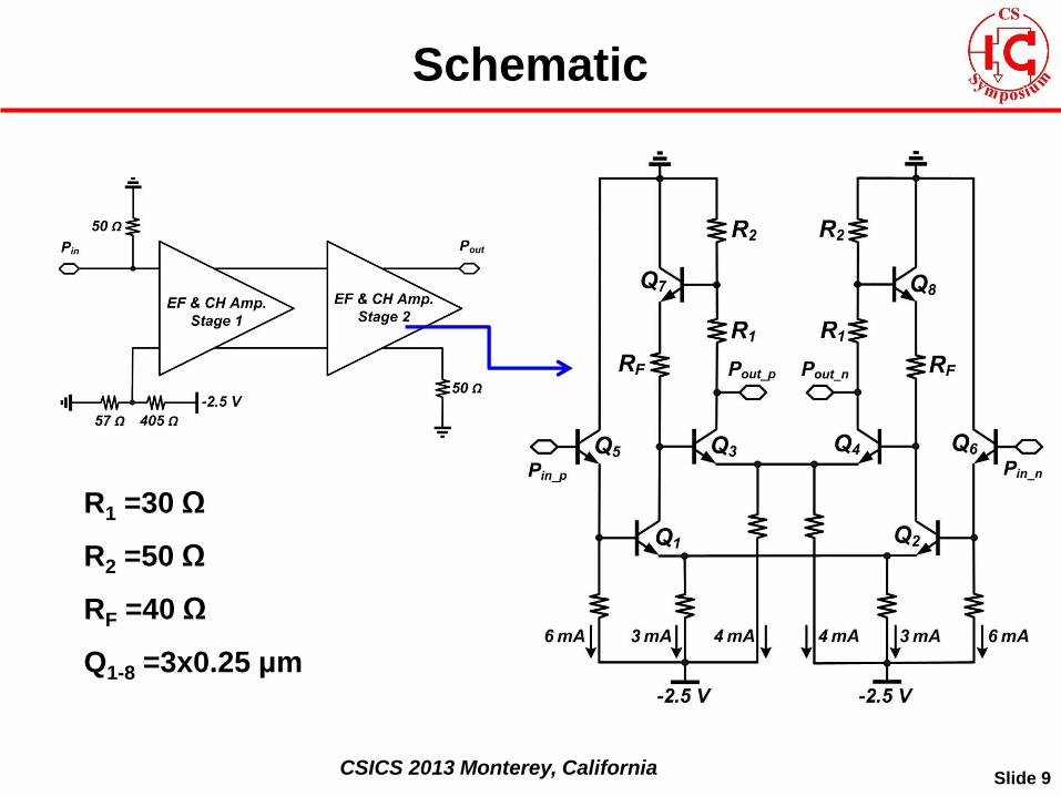
Schematic
Slide 9
R1 =30 Ω
R2 =50 Ω
RF =40 Ω
Q1-8 =3x0.25 μm
CSICS 2013 Monterey, California
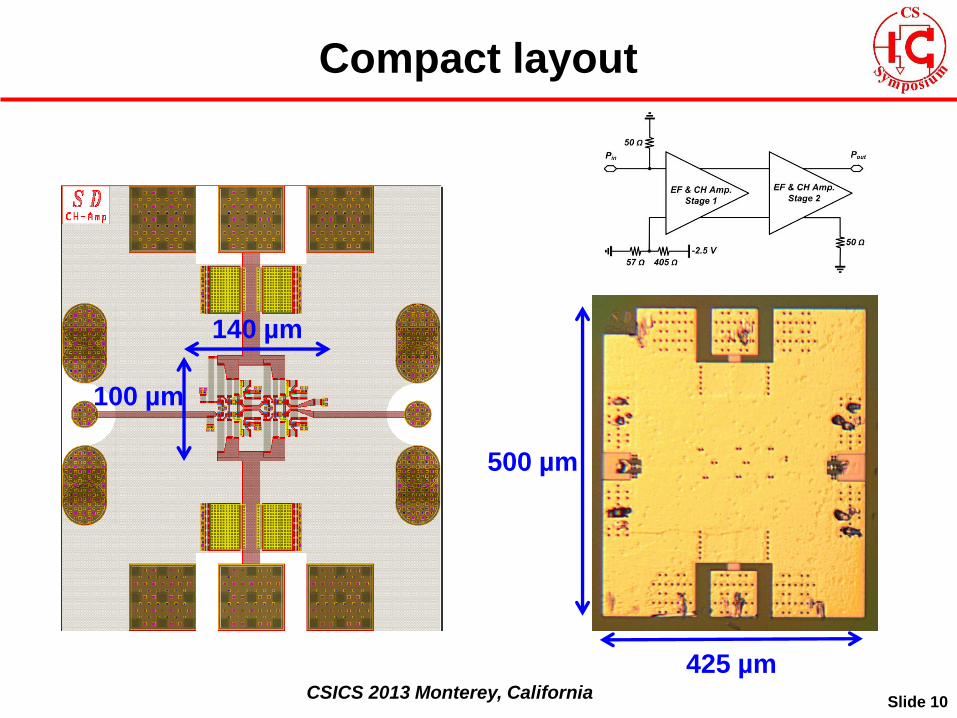
Compact layout
Slide 10
425 µm
500 µm
140 µm
100 µm
CSICS 2013 Monterey, California
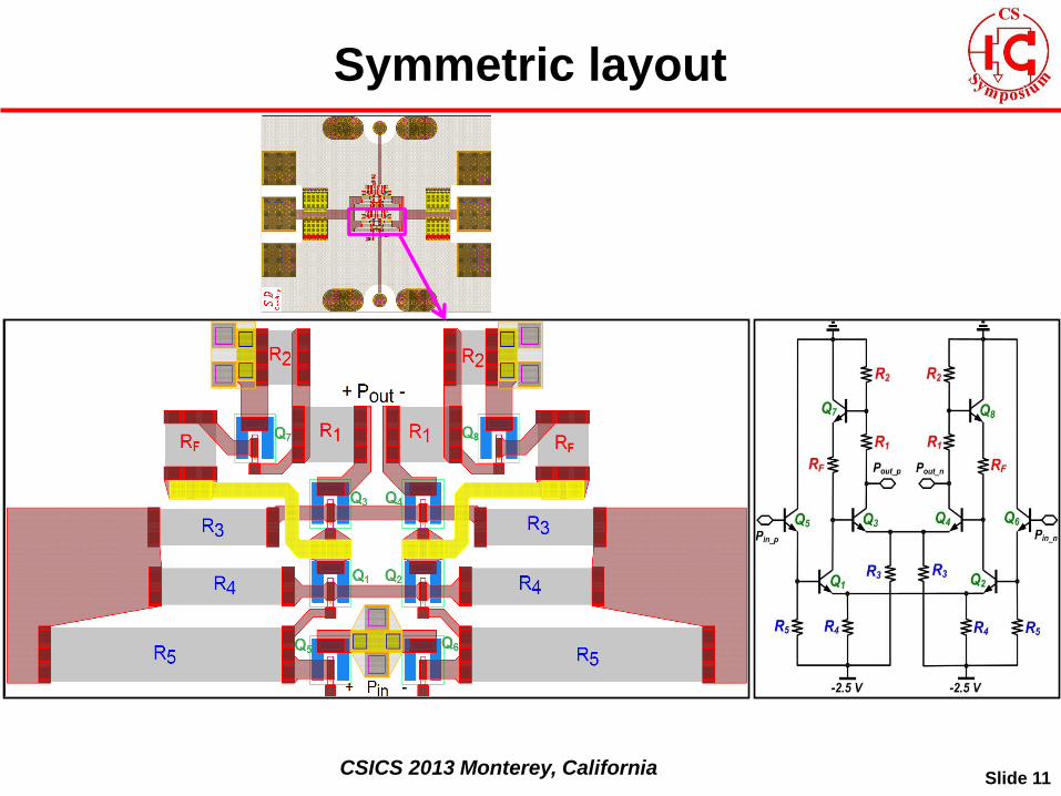
Symmetric layout
Slide 11
CSICS 2013 Monterey, California
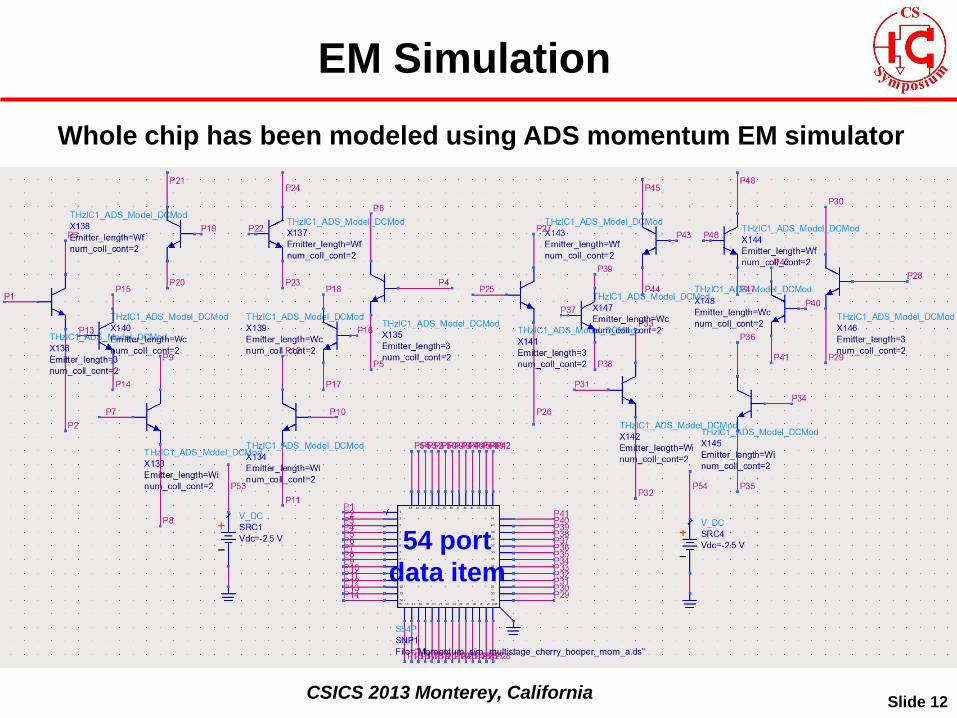
EM Simulation
Slide 12
54 port
data item
Whole chip has been modeled using ADS momentum EM simulator
CSICS 2013 Monterey, California
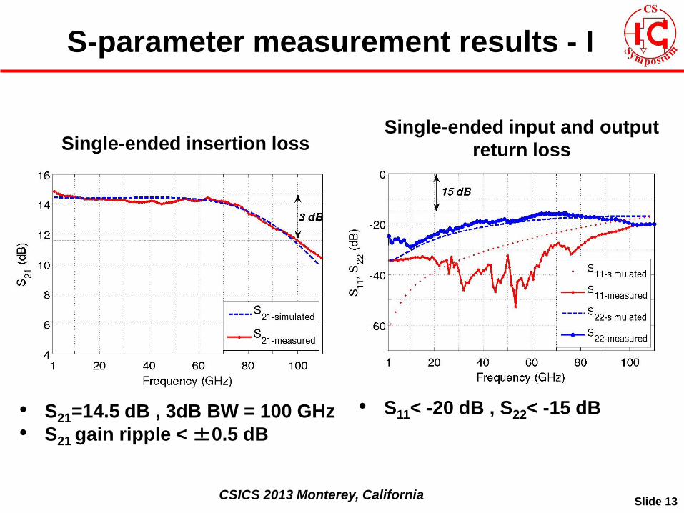
S-parameter measurement results - I
Slide 13
Single-ended insertion loss Single-ended input and output
return loss
• S21=14.5 dB , 3dB BW = 100 GHz
• S21 gain ripple < ±0.5 dB
• S11< -20 dB , S22< -15 dB
CSICS 2013 Monterey, California
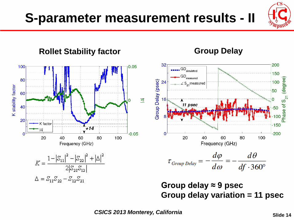
S-parameter measurement results - II
Slide 14
Rollet Stability factor Group Delay
Group delay ≈ 9 psec
Group delay variation = 11 psec
CSICS 2013 Monterey, California
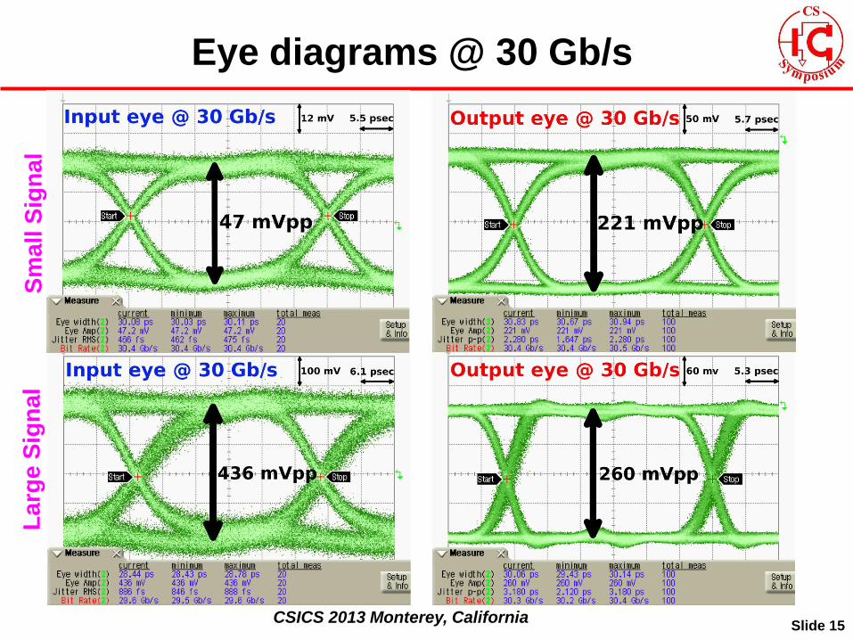
Eye diagrams @ 30 Gb/s
Slide 15
Sm
all S
ign
al
Larg
e S
ign
al
CSICS 2013 Monterey, California
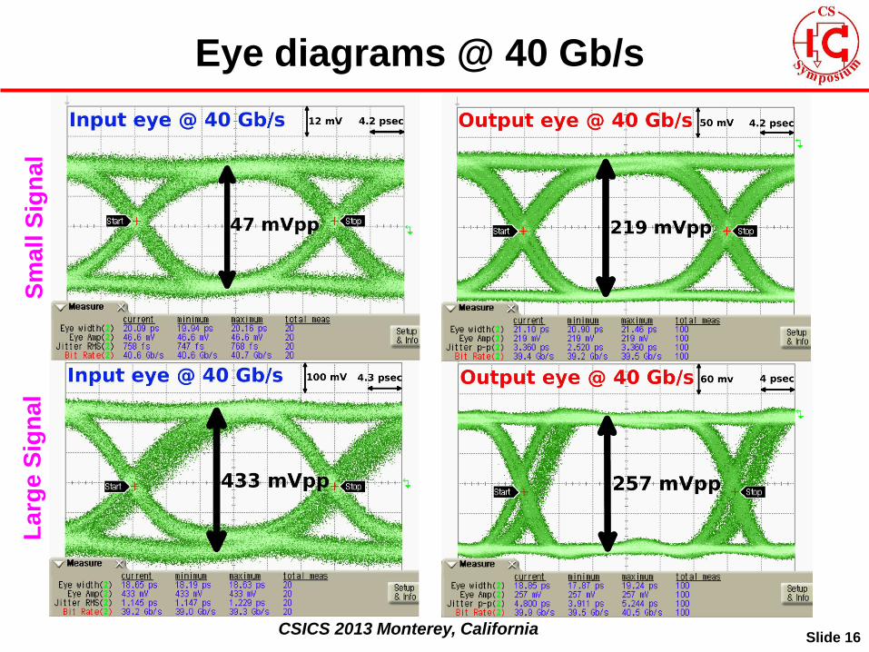
Eye diagrams @ 40 Gb/s
Slide 16
Sm
all S
ign
al
Larg
e S
ign
al
CSICS 2013 Monterey, California
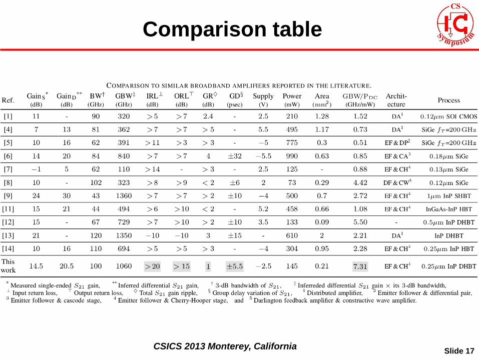
Comparison table
Slide 17
CSICS 2013 Monterey, California
Slide 18
Thank you for your listening


![Cree, CGHV1J070D 70W, DC-18 GHz GaN HEMT DIE (Cree) · vikmwxivihxvehiqevowsj'vii -rg 3xlivxvehiqevow tvshygxerhgsqter] ... 2.00 ghz 0.957 -175.28 2.72 58.56 0.009 -29.21 0.725 -164.11](https://static.fdocument.org/doc/165x107/5b5ac8947f8b9a302a8c8d43/cree-cghv1j070d-70w-dc-18-ghz-gan-hemt-die-cree-vikmwxivihxvehiqevowsjvii.jpg)