ELECTRONICS - home.elka.pw.edu.pl
47
ELECTRONICS SEMICONDUCTOR ELEMENTS 1
Transcript of ELECTRONICS - home.elka.pw.edu.pl

ELECTRONICSSEMICONDUCTOR ELEMENTS
1
QUESTIONS
• What is the Ohm Law formula for calculating voltage across a resistor ?
• Given the current Kirchoffs Law:
σ𝒌 𝒊𝒌 = 𝟎, while
𝒌 = 𝟏, 𝟐, 𝟑, and
𝒊𝟏 = 𝟕𝒎𝑨, 𝒊𝟐 = 𝟑𝒎𝑨,
what is the value of 𝒊𝟑 ? 𝒊𝟑 = −𝟏𝟎𝒎𝑨
• What is the equivalent resistance, between
points A and C, for the given circuit? 10𝛀
• What is the equivalent capacitance?
𝟏. 𝟎𝟎𝟏𝒎𝑭
9
𝒊𝟐𝒊𝟏
𝒊𝟑
𝑨
𝑪
𝑩
𝑨 𝑩𝟐𝒖𝑭 𝟐𝒖𝑭
𝟏𝒎𝑭
𝟑𝛀 6𝛀
𝟖𝛀
𝟐𝛀
𝐔 = 𝐈 ⋅ 𝑹

DIODES
10
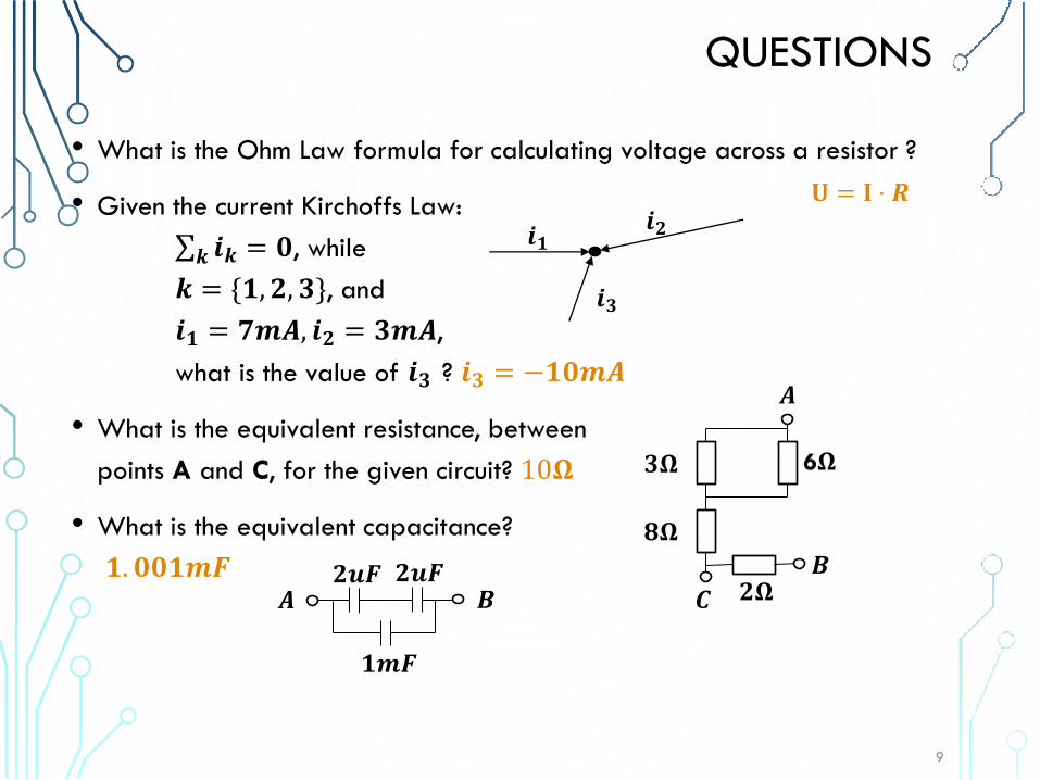
SEMICONDUCTOR DIODE
• Diode is an element utilizing pn junction,
placed in a case with connectors
Diode symbol
11

PERFECT DIODE OPERATION
• Perfect diode can be modeled as a directional valve
• With forward polarization
(anode potential higher than cathode`s)
the circuit is closed
• With reverse polarization
(cathode potential higher than anode`s)
the circuit is open
12
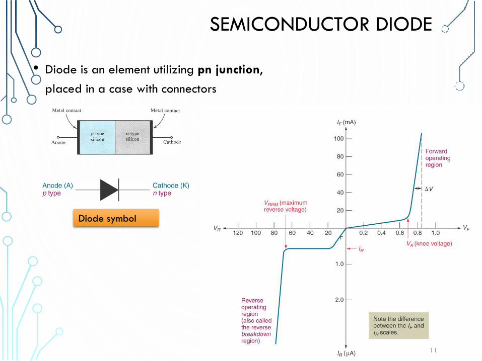
ACTUAL DIODE OPERATION
• With forward polarization
• Conduction begins when the voltage reaches knee voltage
• A voltage drop occurs – depending on the particular diode and the current drawn,
thevoltage is usually ~0.7V, it can be always read from the characteristics
• Power dissipated is calculated as P=U*I
• With reverse polarization
• Reverse current of a few µA flows
• Power dissipated is „negligible”
• Exceeding the maximum reverse
voltage can break the diode
13
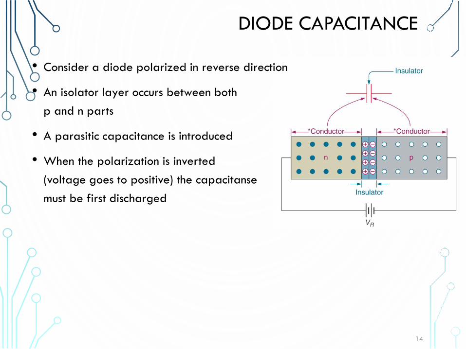
DIODE CAPACITANCE
• Consider a diode polarized in reverse direction
• An isolator layer occurs between both
p and n parts
• A parasitic capacitance is introduced
• When the polarization is inverted
(voltage goes to positive) the capacitanse
must be first discharged
14

TEMPERATURE DEPENDENCE
• Given a constant current flow, the voltage drop across a conducting diode
drops by 2mV/1degC
• The warmer the diode, the lower the voltage drop, and thus the power
dissipated.
• With rising temperature, the reverse current rises too.
15
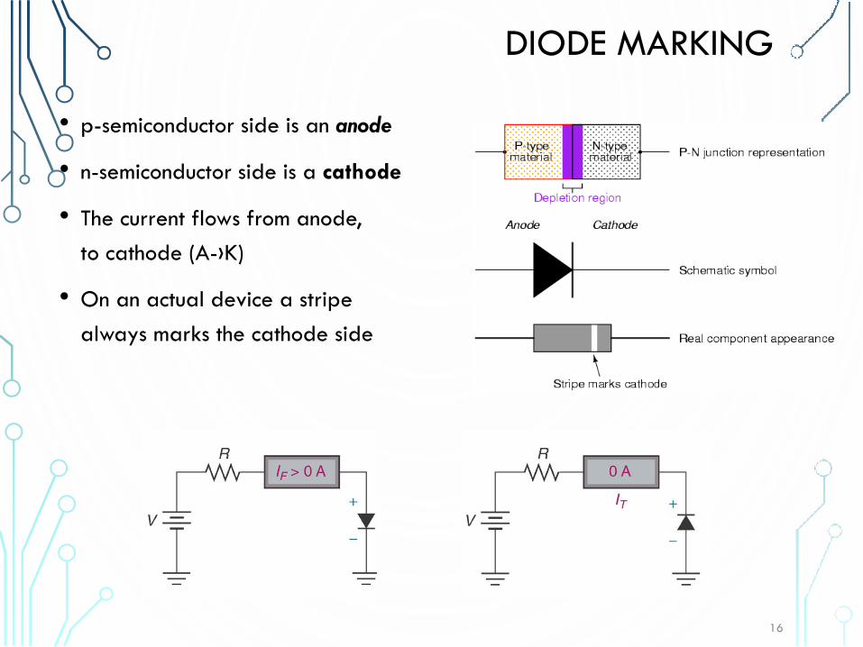
DIODE MARKING
• p-semiconductor side is an anode
• n-semiconductor side is a cathode
• The current flows from anode,
to cathode (A-›K)
• On an actual device a stripe
always marks the cathode side
16

DIODE PARAMETERS I
• Maximum repetitive reverse voltage VRRM [V]
• Reverse voltage that can be periodically applied to the diode.
• Maximum DC reverse voltage VR or VDC [V]
• Reverse voltage that can be constantly applied to the diode.
• Maximum forward voltage VF [V]
• Forward voltage drop given for the nominal current flowing forward.
• Maximum (average) forward current IF(AV ) [A]
• Maximum forward current. The limit is a result from thermal power dissipation capabilities.
• Maximum peak/surge forward current IFSM [A]
• Peak current that can be applied to diode according to a specified pattern (for example a single pulse for a given duration)
17
DIODE PARAMETERS II
• Total power dissipation PD [W]
• The amount of power that can be dissipated from diode to the outside.
• Maximum operating junction temperature TJ [°C]
• Maximum temperaturę, that the junction can operate at, without breaking.
• Thermal resistance R(T) [°C/W]
• Parameter for calculation of the internal temperature at given powerdissipated.
• Reverse (leakage) current IR [µA]
• Reverse current flowing at given negative voltage.
• Typical junction capacitance CJ [pF]
• Typical capacitance, usually expressed in pF.
• Reverse recovery time trr [µs]
• Time for the diode to regain blocking capabilities after voltage polatitychange.
18
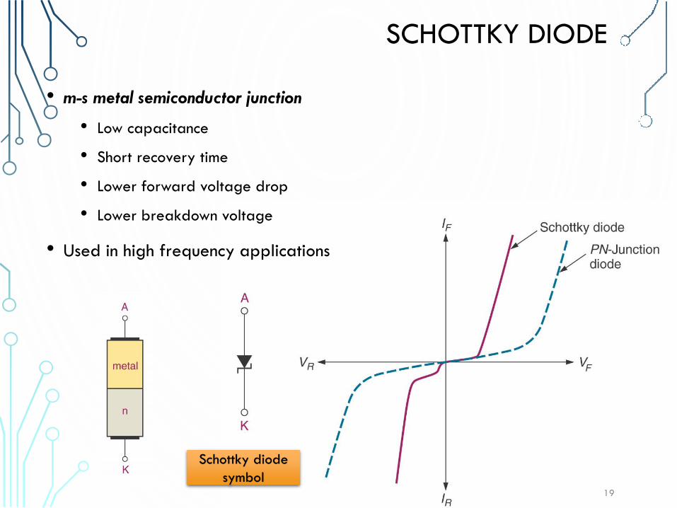
SCHOTTKY DIODE
• m-s metal semiconductor junction
• Low capacitance
• Short recovery time
• Lower forward voltage drop
• Lower breakdown voltage
• Used in high frequency applications
Schottky diode
symbol19

PN & SCHOTTKY COMPARSION
20

DIODES IN PRACTICE
• Example datasheet
• Typical packages
21

DIODE MODELS
Real Ideal Simplified Linearized
According to Shockley’s
equation
No reverse current, no
forward voltageForward voltage
considered
Linear approximation
of the characteristics
22
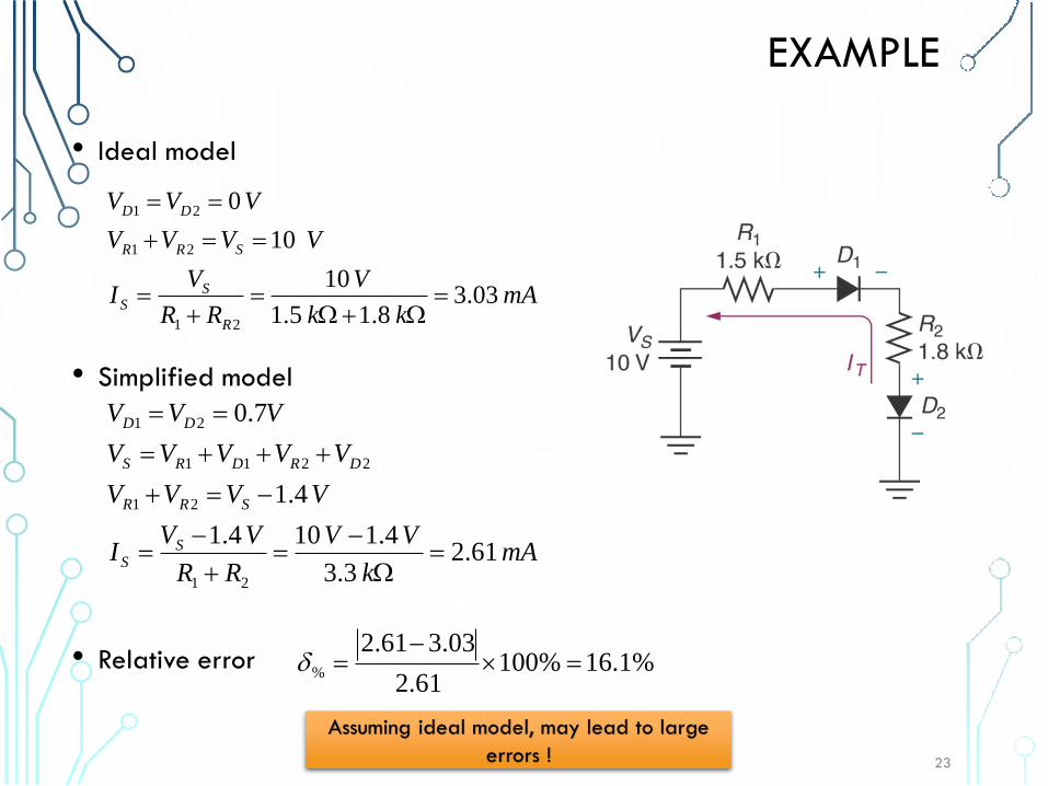
EXAMPLE
• Ideal model
• Simplified model
• Relative error
mAkk
V
RR
VI
VVVV
VVV
R
SS
SRR
DD
03.38.15.1
10
10
0
21
21
21
=+
=+
=
==+
==
mAk
VV
RR
VVI
VVVV
VVVVV
VVV
SS
SRR
DRDRS
DD
61.23.3
4.1104.1
4.1
7.0
21
21
2211
21
=
−=
+
−=
−=+
+++=
==
%1.16%10061.2
03.361.2% =
−=
Assuming ideal model, may lead to large
errors ! 23

DIODE TESTING
• Resistance measurement
• Forward polarization should give a resistance of <1kΩ
• Reverse polarization should give
a resistance of >1MΩ
or out of scale
• Diode testing mode
• Polarized in forward direction should give ~0,7V
• Reverse polarization should
occur as open circuit
24
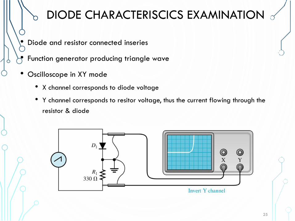
DIODE CHARACTERISCICS EXAMINATION
• Diode and resistor connected inseries
• Function generator producing triangle wave
• Oscilloscope in XY mode
• X channel corresponds to diode voltage
• Y channel corresponds to resitor voltage, thus the current flowing through the
resistor & diode
25

ZENER DIODE
26
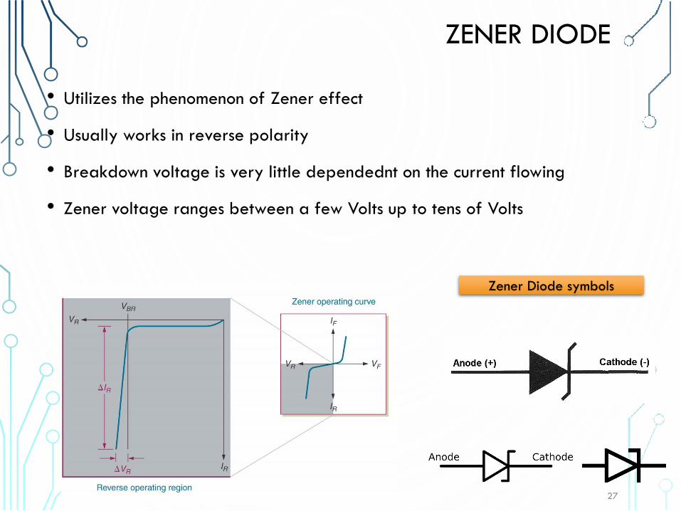
ZENER DIODE
• Utilizes the phenomenon of Zener effect
• Usually works in reverse polarity
• Breakdown voltage is very little dependednt on the current flowing
• Zener voltage ranges between a few Volts up to tens of Volts
Zener Diode symbols
27
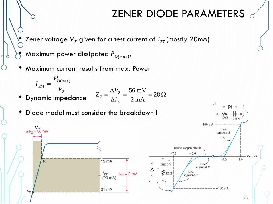
ZENER DIODE PARAMETERS
• Zener voltage VZ given for a test current of IZT (mostly 20mA)
• Maximum power dissipated PD(max),
• Maximum current results from max. Power
• Dynamic impedance
• Diode model must consider the breakdown !
Z
D
ZMV
PI
(max)=
==
= 28
mA2
mV56
Z
ZZ
I
VZ
VZ
28
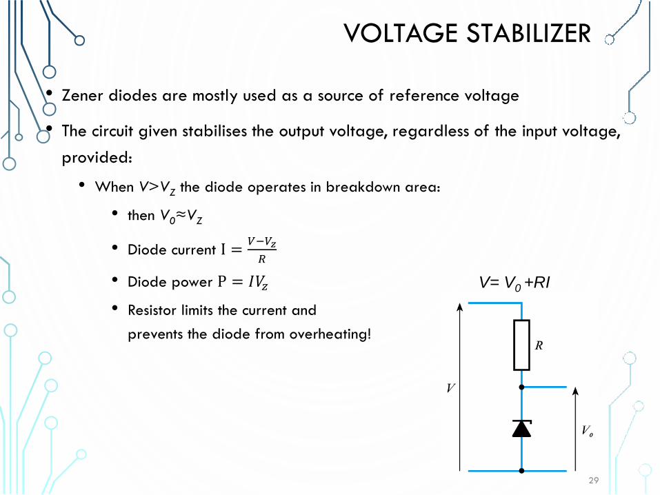
VOLTAGE STABILIZER
• Zener diodes are mostly used as a source of reference voltage
• The circuit given stabilises the output voltage, regardless of the input voltage,
provided:
• When V>VZ the diode operates in breakdown area:
• then V0≈VZ
• Diode current I =𝑉−𝑉𝑧
𝑅
• Diode power P = 𝐼𝑉𝑧
• Resistor limits the current and
prevents the diode from overheating!
V= V0 +RI
29

GRAHICAL ANALYSIS
• Operating point moves when changing the source voltage
• Output voltage depends on the steepness of the characteristics,
thus it depends on dynamic impedance
30
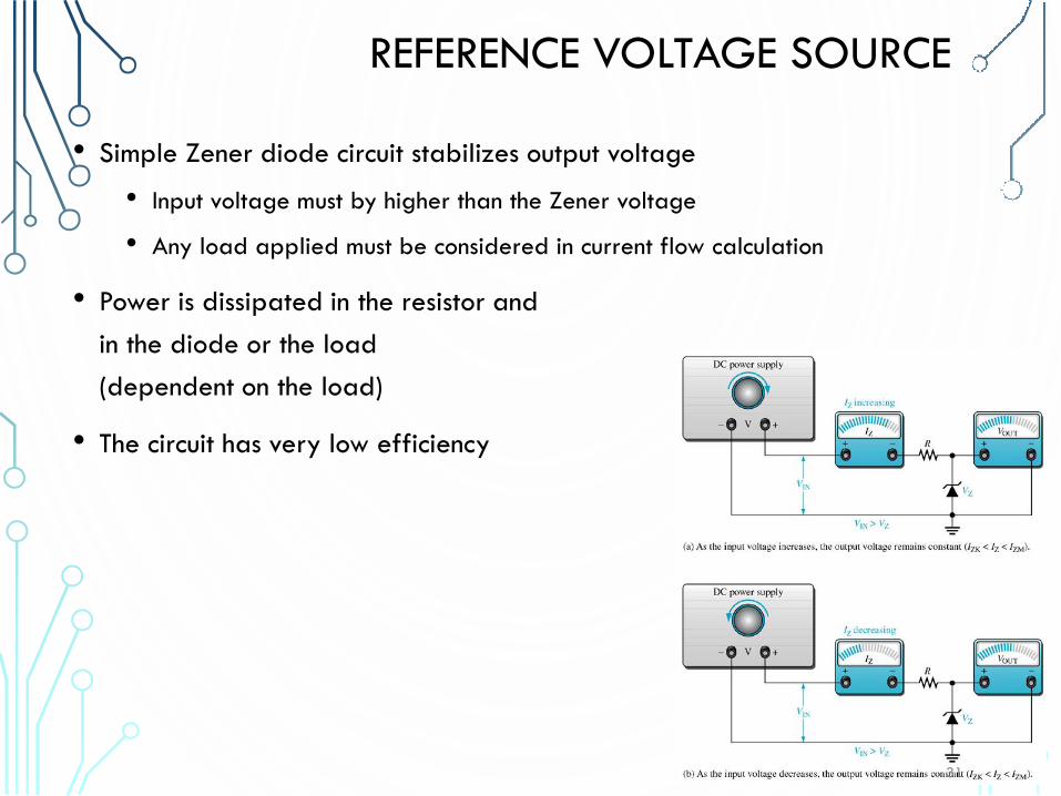
REFERENCE VOLTAGE SOURCE
• Simple Zener diode circuit stabilizes output voltage
• Input voltage must by higher than the Zener voltage
• Any load applied must be considered in current flow calculation
• Power is dissipated in the resistor and
in the diode or the load
(dependent on the load)
• The circuit has very low efficiency
31

SIMPLE APPLICATIONS
32
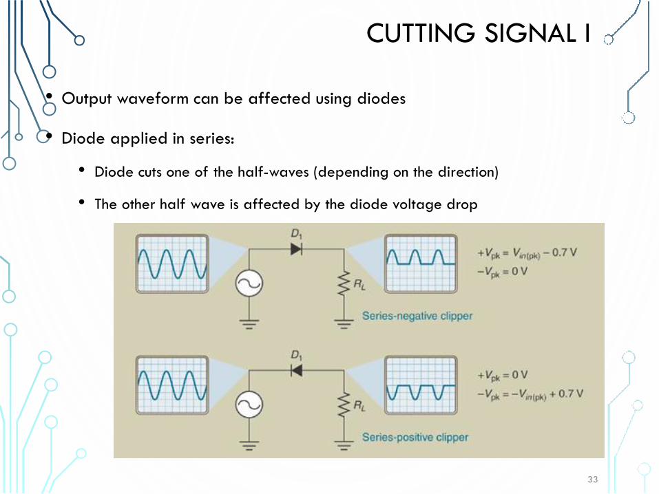
CUTTING SIGNAL I
• Output waveform can be affected using diodes
• Diode applied in series:
• Diode cuts one of the half-waves (depending on the direction)
• The other half wave is affected by the diode voltage drop
33
CUTTING SIGNAL II
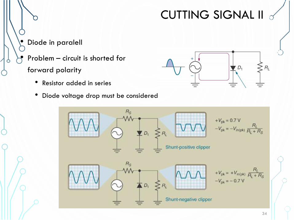
• Diode in paralell
• Problem – circuit is shorted for
forward polarity
• Resistor added in series
• Diode voltage drop must be considered
34
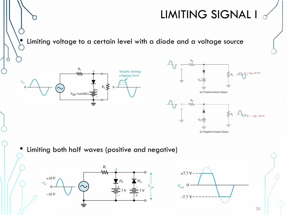
LIMITING SIGNAL I
• Limiting voltage to a certain level with a diode and a voltage source
• Limiting both half waves (positive and negative)
35
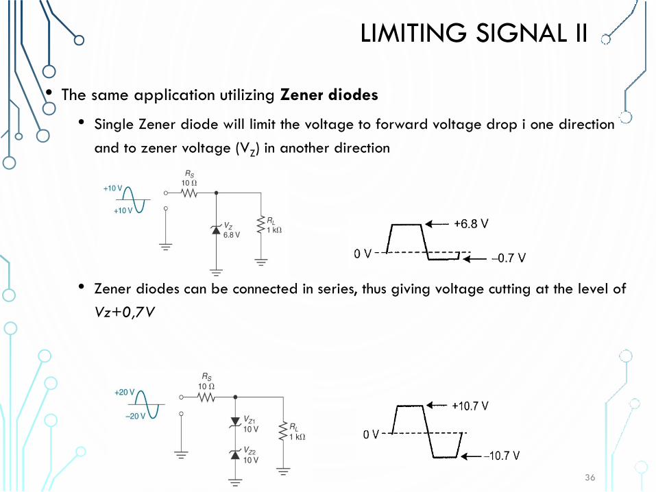
LIMITING SIGNAL II
• The same application utilizing Zener diodes
• Single Zener diode will limit the voltage to forward voltage drop i one direction
and to zener voltage (VZ) in another direction
• Zener diodes can be connected in series, thus giving voltage cutting at the level of
Vz+0,7V
36
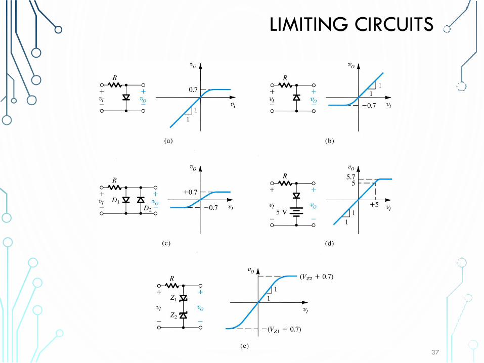
LIMITING CIRCUITS
37

VOLTAGE SPIKES PROTECTION
• Voltage spikes protection:
• Must withstand big energies for short periods of time
• Must react instantly
• Zener diodes and both Transil diodes (or TVS) may be used
• Transil (TVS - transient voltage supressor) is a specialized diode designed for
suppresing high voltage spikes
• Example protection circuit:
Transil symbol
38
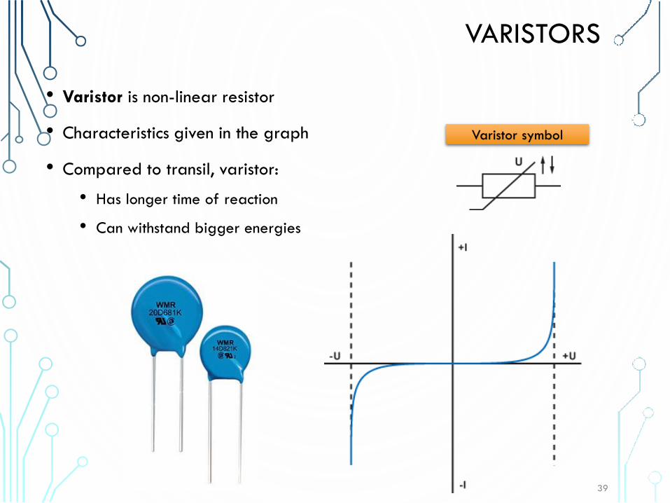
VARISTORS
• Varistor is non-linear resistor
• Characteristics given in the graph
• Compared to transil, varistor:
• Has longer time of reaction
• Can withstand bigger energies
Varistor symbol
39
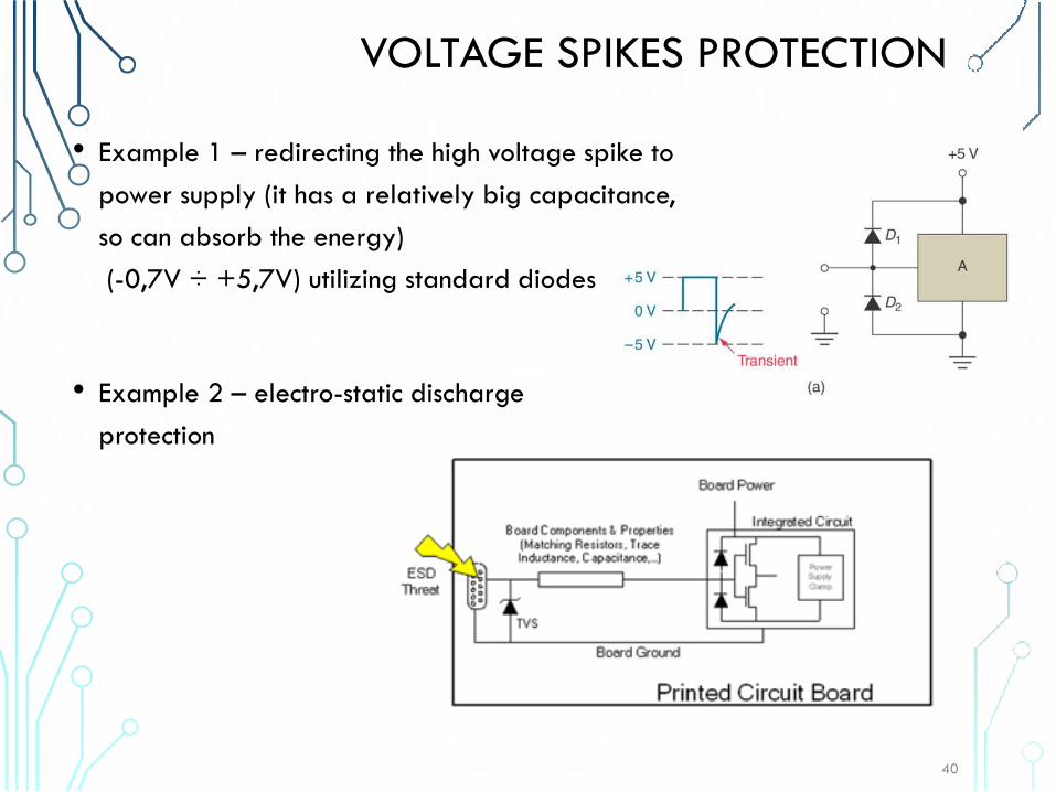
VOLTAGE SPIKES PROTECTION
• Example 1 – redirecting the high voltage spike to
power supply (it has a relatively big capacitance,
so can absorb the energy)
(-0,7V ÷ +5,7V) utilizing standard diodes
• Example 2 – electro-static discharge
protection
40
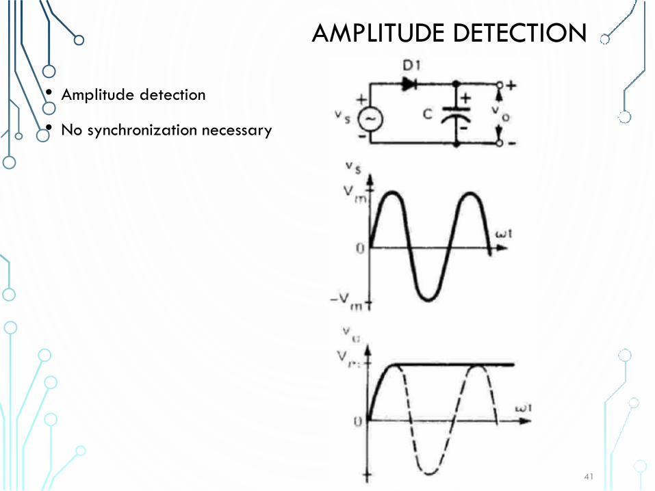
AMPLITUDE DETECTION
41
• Amplitude detection
• No synchronization necessary

AMPLITUDE DETECTION
• Demodulation of a signal (AM radio signal)
• Proper selection of components RLC1 allows to filter the signal and find its corresponding
„envelope”
42
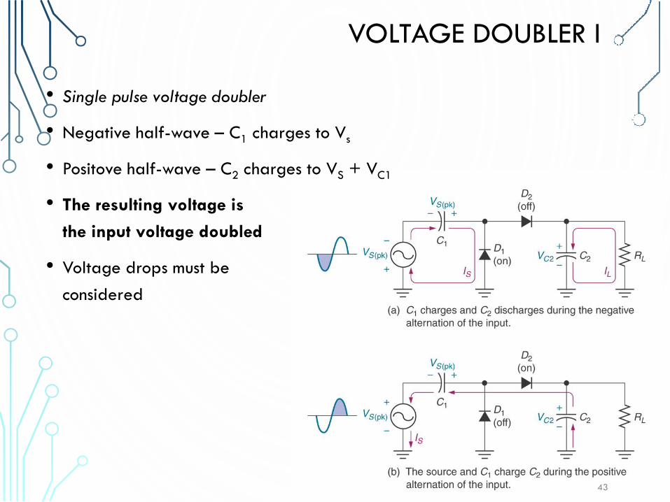
VOLTAGE DOUBLER I
• Single pulse voltage doubler
• Negative half-wave – C1 charges to Vs
• Positove half-wave – C2 charges to VS + VC1
• The resulting voltage is
the input voltage doubled
• Voltage drops must be
considered
43
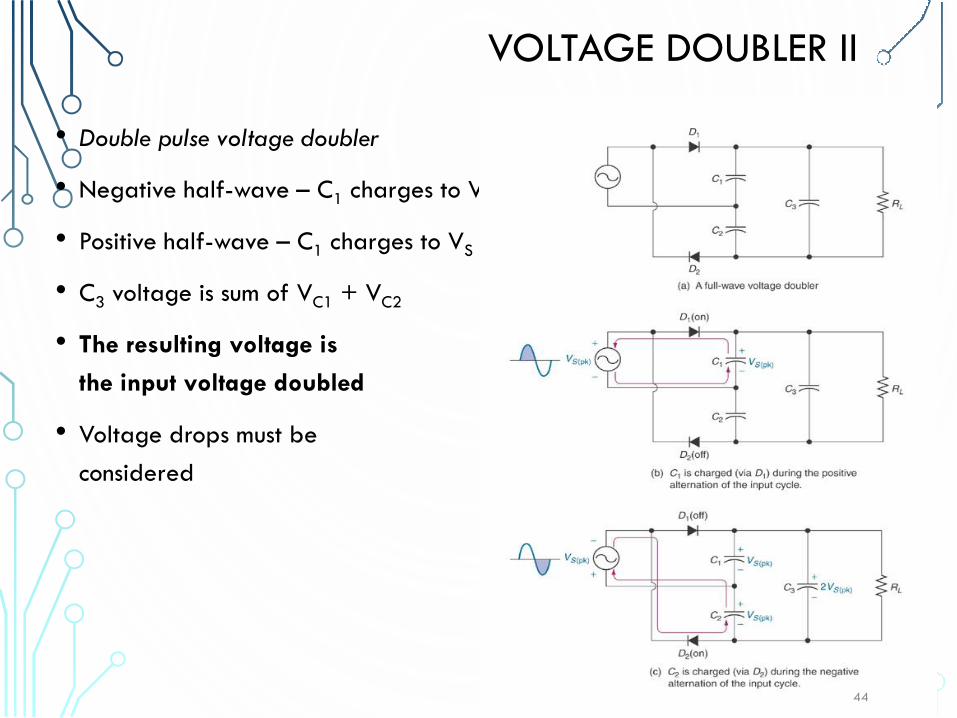
VOLTAGE DOUBLER II
• Double pulse voltage doubler
• Negative half-wave – C1 charges to VS
• Positive half-wave – C1 charges to VS
• C3 voltage is sum of VC1 + VC2
• The resulting voltage is
the input voltage doubled
• Voltage drops must be
considered
44
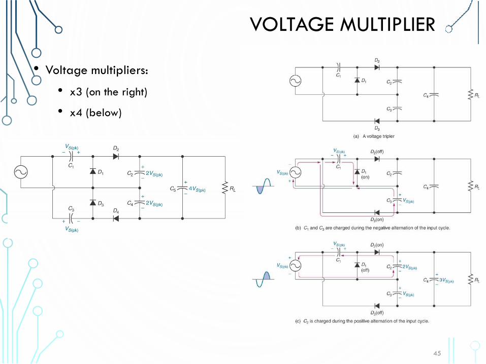
VOLTAGE MULTIPLIER
• Voltage multipliers:
• x3 (on the right)
• x4 (below)
45

OPTO-ELECTRONICS
46
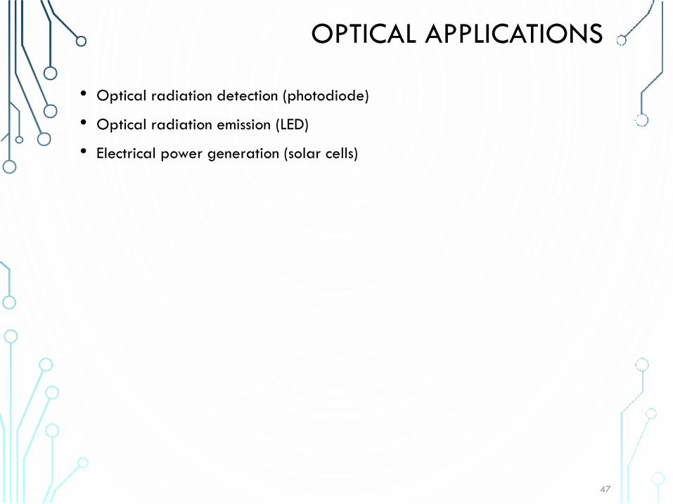
OPTICAL APPLICATIONS
• Optical radiation detection (photodiode)
• Optical radiation emission (LED)
• Electrical power generation (solar cells)
47

PHOTODIODE
• Works in reverse polarity
• Current proportional to light flux
Photodiode symbol
48

LED I
• LED – light-emitting diode
• Color (wavelength) depends on the
semiconductor type used
• Radiation intensity is proportional
to the current flowing
49
LED symbol
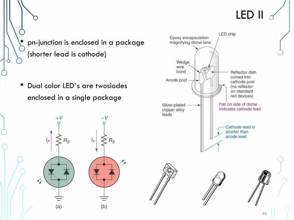
LED II
• pn-junction is enclosed in a package
(shorter lead is cathode)
• Dual color LED`s are twosiodes
enclosed in a single package
50

SELECTING LED RESISTOR
• Diodes are usually designed for the current of 5-20mA
• Resistor selection, given the source voltage, diode voltage drop
and diode nominal current
( )
( )
1.8...2.0
20
8
8 1.8310
20
F
F
out pk
out pk F
S
F
V V
I mA
V V
V V V VR
I mA
=
=
=
− −= = =
51
LED APPLICATIONS
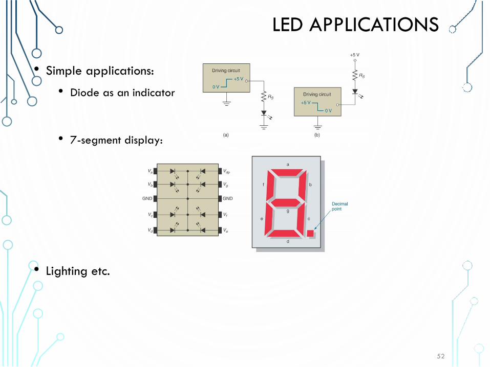
• Simple applications:
• Diode as an indicator
• 7-segment display:
• Lighting etc.
52
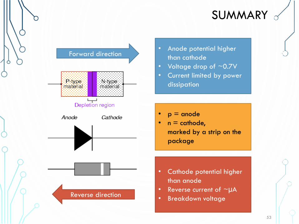
SUMMARY
Forward direction
Reverse direction
• Anode potential higher
than cathode
• Voltage drop of ~0.7V
• Current limited by power
dissipation
• Cathode potential higher
than anode
• Reverse current of ~µA
• Breakdown voltage
• p = anode
• n = cathode,
marked by a strip on the
package
53

THANK YOU
54


![GATE 2021 [Afternoon Session] 1 Electronics ...](https://static.fdocument.org/doc/165x107/61f934f172f3ef648a782147/gate-2021-afternoon-session-1-electronics-.jpg)