VN340SP-33-E, VN340SPTR-33-E - st.com · = 10 to 36 V; V IN =V IL 50 μA t SC Delay time of current...
19
September 2015 DocID11471 Rev 4 1/19 This is information on a product in full production. www.st.com VN340SP-33-E Quad high-side smart power solid-state relay Datasheet - production data Features Type Vdemag (1) RDS(on) (1) IOUT (1) VCC VN340SP-33-E VCC-55 V 0.2 Ω 1 A 36 V Notes: (1) Per channel Output current: 1 A per channel Digital I/O clamped at 32 V minimum voltage Shorted load and overtemperature protections Protection against loss of ground Built-in current limiter Undervoltage shutdown Open drain diagnostic output Fast demagnetization of inductive loads Conforms to IEC 61131-2 Description The VN340SP-33-E is a monolithic device developed using STMicroelectronics' VIPower technology, intended to drive four independent resistive or inductive loads with one side connected to ground. Active current limitation prevents dropping of the system power supply in case of shorted load. Built-in thermal shutdown protects the chip from overtemperature and short-circuit. The open drain diagnostic output indicates overtemperature conditions. Each I/O is pulled down when the overtemperature condition of the relative channel is verified. Table 1: Device summary Order code Package Packing VN340SP-33-E PowerSO-10 Tube VN340SPTR-33-E Tape and reel PowerSO-10
Transcript of VN340SP-33-E, VN340SPTR-33-E - st.com · = 10 to 36 V; V IN =V IL 50 μA t SC Delay time of current...
September 2015 DocID11471 Rev 4 1/19
This is information on a product in full production. www.st.com
VN340SP-33-E
Quad high-side smart power solid-state relay
Datasheet - production data
Features
Type Vdemag(1)
RDS(on)(1)
IOUT(1)
VCC
VN340SP-33-E VCC-55 V 0.2 Ω 1 A 36 V
Notes: (1)
Per channel
Output current: 1 A per channel
Digital I/O clamped at 32 V minimum voltage
Shorted load and overtemperature protections
Protection against loss of ground
Built-in current limiter
Undervoltage shutdown
Open drain diagnostic output
Fast demagnetization of inductive loads
Conforms to IEC 61131-2
Description The VN340SP-33-E is a monolithic device developed using STMicroelectronics' VIPower technology, intended to drive four independent resistive or inductive loads with one side connected to ground. Active current limitation prevents dropping of the system power supply in case of shorted load. Built-in thermal shutdown protects the chip from overtemperature and short-circuit. The open drain diagnostic output indicates overtemperature conditions. Each I/O is pulled down when the overtemperature condition of the relative channel is verified.
Table 1: Device summary
Order code Package Packing
VN340SP-33-E PowerSO-10
Tube
VN340SPTR-33-E Tape and reel
PowerSO-10
Contents VN340SP-33-E
2/19 DocID11471 Rev 4
Contents
1 Block diagram .................................................................................. 5
2 Pin connection ................................................................................. 6
3 Maximum ratings ............................................................................. 7
4 Electrical characteristics ................................................................ 8
5 Test circuits ................................................................................... 10
6 Switching time waveforms and truth table .................................. 12
7 Package information ..................................................................... 14
7.1 PowerSO-10 package information .................................................. 14
7.2 PowerSO-10 packing information .................................................... 16
8 Revision history ............................................................................ 18
VN340SP-33-E List of tables
DocID11471 Rev 4 3/19
List of tables
Table 1: Device summary ........................................................................................................................... 1 Table 2: Absolute maximum ratings ........................................................................................................... 7 Table 3: Thermal data ................................................................................................................................. 7 Table 4: Power section ............................................................................................................................... 8 Table 5: Switching (VCC = 24 V, TJ= 25 °C ) ............................................................................................... 8 Table 6: Logic inputs ................................................................................................................................... 9 Table 7: Protection and diagnostic ............................................................................................................. 9 Table 8: Truth table ................................................................................................................................... 13 Table 9: PowerSO-10 package mechanical data ..................................................................................... 15 Table 10: PowerSO-10 career tape dimension mechanical data ............................................................. 16 Table 11: PowerSO-10 reel dimension mechanical data ......................................................................... 17 Table 12: PowerSO-10 base and bulk quantity ........................................................................................ 17 Table 13: Document revision history ........................................................................................................ 18
List of figures VN340SP-33-E
4/19 DocID11471 Rev 4
List of figures
Figure 1: Block diagram .............................................................................................................................. 5 Figure 2: Connection diagram (top view) .................................................................................................... 6 Figure 3: Current and voltage conventions ................................................................................................. 6 Figure 4: Avalanche energy test circuit ..................................................................................................... 10 Figure 5: Peak short-circuit test diagram .................................................................................................. 10 Figure 6: ILGND test configuration ............................................................................................................... 11 Figure 7: Switching waveforms ................................................................................................................. 12 Figure 8: Switching parameter test conditions .......................................................................................... 12 Figure 9: Driving circuit ............................................................................................................................. 13 Figure 10: PowerSO-10 package outline .................................................................................................. 14 Figure 11: PowerSO-10 career tape outline ............................................................................................. 16 Figure 12: PowerSO-10 reel outline ......................................................................................................... 17
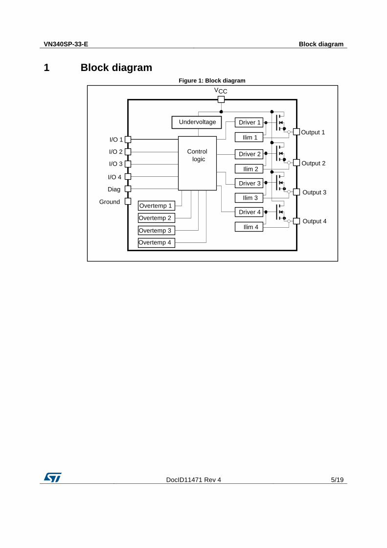
VN340SP-33-E Block diagram
DocID11471 Rev 4 5/19
1 Block diagram Figure 1: Block diagram
Undervoltage Driver 1
Ilim 1
Ilim 2
Driver 2
Driver 3
Ilim 3
Driver 4
Ilim 4
Overtemp 1
Overtemp 2
Overtemp 3
Overtemp 4
Output 4
Output 3
Output 2
Output 1
Ground
Diag
I/O 4
I/O 3
I/O 2
I/O 1
Control
logic
VCC
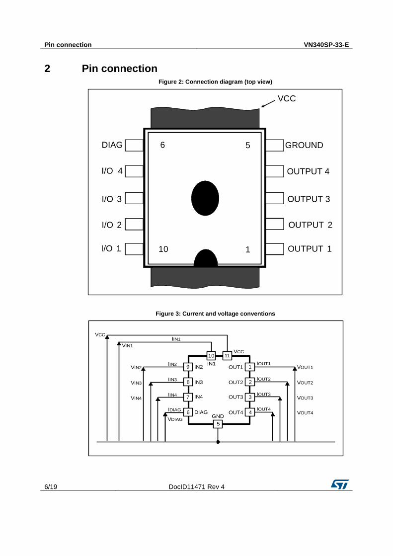
Pin connection VN340SP-33-E
6/19 DocID11471 Rev 4
DIAG
1
VCC
5
10
6
I/O 4
I/O 3
I/O 2
I/O 1
GROUND
OUTPUT 4
OUTPUT 3
OUTPUT 2
OUTPUT 1
GND
1
2
3
4
5
9
8
7
6
10 11
DIAG
IN4
IN3
IN2
OUT4
OUT3
OUT2
OUT1IN1
VCC
VCC
IOUT1
IIN1
IOUT2
IOUT3
IOUT4
IIN2
IIN3
IIN4
IDIAG
VOUT1
VOUT2
VOUT3
VOUT4
VIN2
VIN1
VIN3
VIN4
VDIAG
2 Pin connection Figure 2: Connection diagram (top view)
Figure 3: Current and voltage conventions
VN340SP-33-E Maximum ratings
DocID11471 Rev 4 7/19
3 Maximum ratings Table 2: Absolute maximum ratings
Symbol Parameter Value Unit
VCC Power supply voltage 45 V
-VCC Reverse supply voltage -4 V
IOUT Output current Internally limited A
IR Reverse output current (per channel) -6 A
IIN Input current range -1 to +10 mA
IDIAG Diag pin current -1 to +10 mA
VESD Electrostatic discharge (R = 1.5 kΩ; C = 100 pF) 2000 V
EAS
Single pulse avalanche energy one channel active
TJ = 125 °, ILOAD = 0.625 A 10 J
Single pulse avalanche energy all channel active
simultaneously TJ = 125 °, ILOAD = 0.625 A 2 J
PTOT Power dissipation at TC = 25 °C Internally limited W
TJ Junction operating temperature Internally limited °C
TSTG Storage temperature -55 to 150 °C
Table 3: Thermal data
Symbol Parameter Value Unit
Rth(JC) Thermal resistance junction-case (1)
Max. 3 °C/W
Rth(JA) Thermal resistance junction-ambient (2)
Max. 50 °C/W
Notes: (1)
Per channel. (2)
When mounted on a four-layer FR4, with the minimum recommended pad size.
Electrical characteristics VN340SP-33-E
8/19 DocID11471 Rev 4
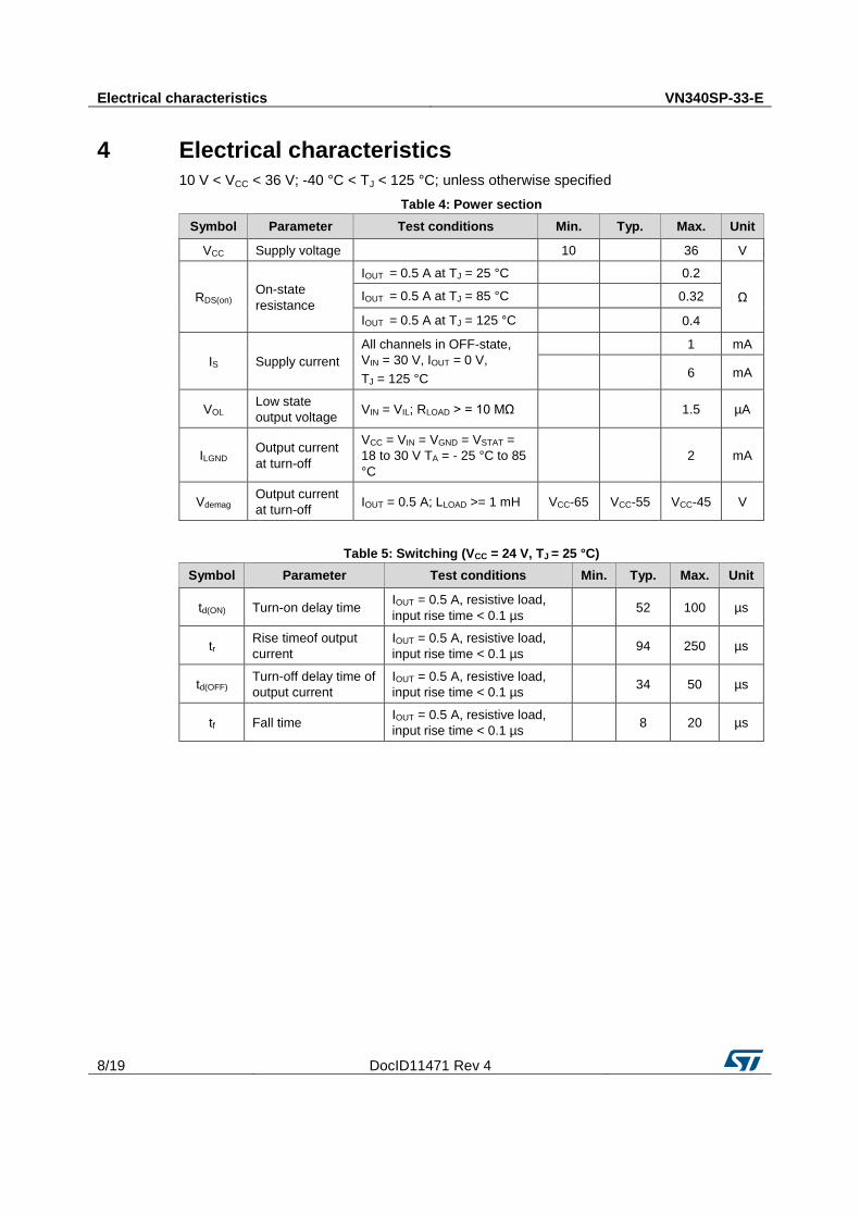
4 Electrical characteristics
10 V < VCC < 36 V; -40 °C < TJ < 125 °C; unless otherwise specified
Table 4: Power section
Symbol Parameter Test conditions Min. Typ. Max. Unit
VCC Supply voltage
10
36 V
RDS(on) On-state
resistance
IOUT = 0.5 A at TJ = 25 °C
0.2
Ω IOUT = 0.5 A at TJ = 85 °C
0.32
IOUT = 0.5 A at TJ = 125 °C
0.4
IS Supply current
All channels in OFF-state,
VIN = 30 V, IOUT = 0 V,
TJ = 125 °C
1 mA
6 mA
VOL Low state
output voltage VIN = VIL; RLOAD > = 10 MΩ
1.5 µA
ILGND Output current
at turn-off
VCC = VIN = VGND = VSTAT =
18 to 30 V TA = - 25 °C to 85
°C 2 mA
Vdemag Output current
at turn-off IOUT = 0.5 A; LLOAD >= 1 mH VCC-65 VCC-55 VCC-45 V
Table 5: Switching (VCC = 24 V, TJ = 25 °C)
Symbol Parameter Test conditions Min. Typ. Max. Unit
td(ON) Turn-on delay time IOUT = 0.5 A, resistive load,
input rise time < 0.1 µs 52 100 µs
tr Rise timeof output
current
IOUT = 0.5 A, resistive load,
input rise time < 0.1 µs 94 250 µs
td(OFF) Turn-off delay time of
output current
IOUT = 0.5 A, resistive load,
input rise time < 0.1 µs 34 50 µs
tf Fall time IOUT = 0.5 A, resistive load,
input rise time < 0.1 µs 8 20 µs
VN340SP-33-E Electrical characteristics
DocID11471 Rev 4 9/19
Table 6: Logic inputs
Symbol Parameter Test conditions Min. Typ. Max. Unit
VIL I/O input low level
voltage 2 V
VIH I/O input high level
voltage 3.5
V
VI(HYST) I/O input hysteresis
voltage 0.5
V
IIN I/O input current VIN = 30 V
25 µA
VICL I/O input clamp
voltage(1)
IIN = 1 mA 32
36
V
IIN = -1 mA -0.7 V
Notes: (1)
The input voltage is internally clamped at 32 V minimum, the input pins can be connected to a higher voltage by an external resistor, which cannot exceed 10 mA
Table 7: Protection and diagnostic
Symbol Parameter Test conditions Min. Typ. Max. Unit
VDIAG(1)
Status voltage
output low IDIAG = 5 mA (fault condition)
1
V
VSCL Status clamp
voltage IDIAG = 1 mA
32 36
-0.7
VUSD Undervoltage
shutdown 5
8 V
Ilim DC short-circuit
current VCC = 24 V; RLOAD < 10 mΩ 1
2 A
IOVPK Peak short-circuit
current
VCC = 24 V; VIN = 30 V;
RLOAD < 10 mΩ 4 V
IDIAGH Leakage on DIAG
pin in high state VDIAG = 24 V
25 μA
ILOAD Output leakage
current VCC = 10 to 36 V; VIN=VIL
50 μA
tSC Delay time of
current limiter 100 μs
TTSD Junction shutdown
temperature 150 170
°C
TR Junction reset
temperature 135 155
°C
Notes: (1)
Status determination > 100 μs after the switching edge.
If the INPUT pin is left floating, the corresponding channel automatically switches off. If GND pin is disconnected, the channel switches off provided that VCC does not exceed 36 V.
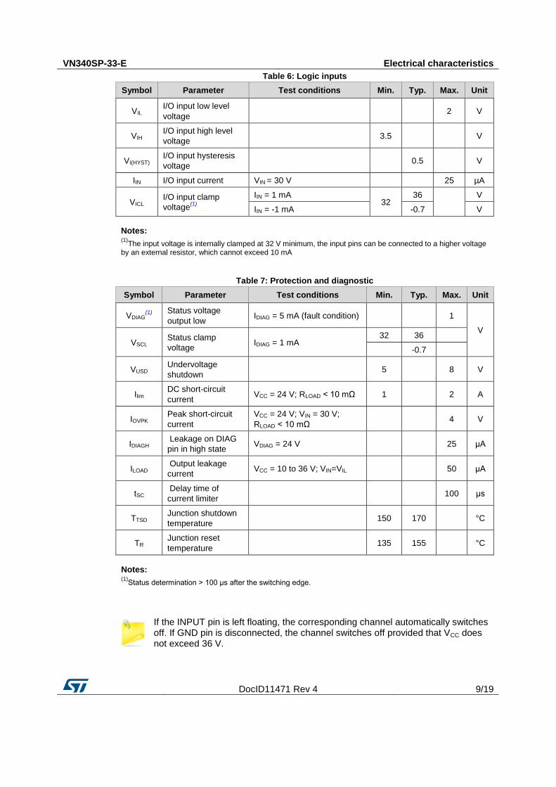
Test circuits VN340SP-33-E
10/19 DocID11471 Rev 4
IN
GND
DIAG
+VCC
OUTPUT
RINCONTROL
UNIT
10 k Ω
GND
LOAD
IN
GND
DIAG
+VCC
OUTPUT
RINCONTROL
UNIT
10kΩ
GNDRL < 10m Ω
5 Test circuits Figure 4: Avalanche energy test circuit
Figure 5: Peak short-circuit test diagram
VN340SP-33-E Test circuits
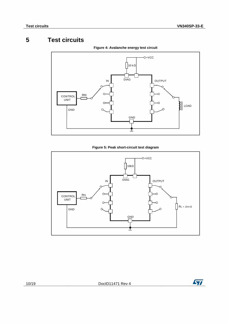
DocID11471 Rev 4 11/19
GND
DIAG
I/On
GND
OUTn
+
A IGND
Figure 6: ILGND test configuration
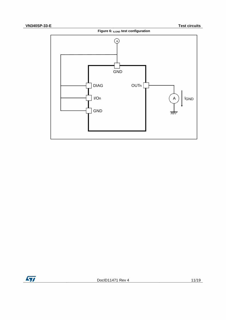
Switching time waveforms and truth table VN340SP-33-E
12/19 DocID11471 Rev 4
Undervoltage
Switch n
I/O n
(=MCONTn)
Iout n
on
off
Normal operation
DIAG
Iout n
I/O n
(=MCONTn)
Switch n
Iout n
on
off
DIAG
Shorted load operation
MCONTn
I/O n
Ilim
DIAG
Switch non
off
IOVPKTj=TTSD Tj=TR
t
t
Vgen
Id
90%
10%
tr tf
tdon tdoff
t = 10 us, repetition rate = 1 ms
6 Switching time waveforms and truth table Figure 7: Switching waveforms
Figure 8: Switching parameter test conditions
VN340SP-33-E Switching time waveforms and truth table
DocID11471 Rev 4 13/19
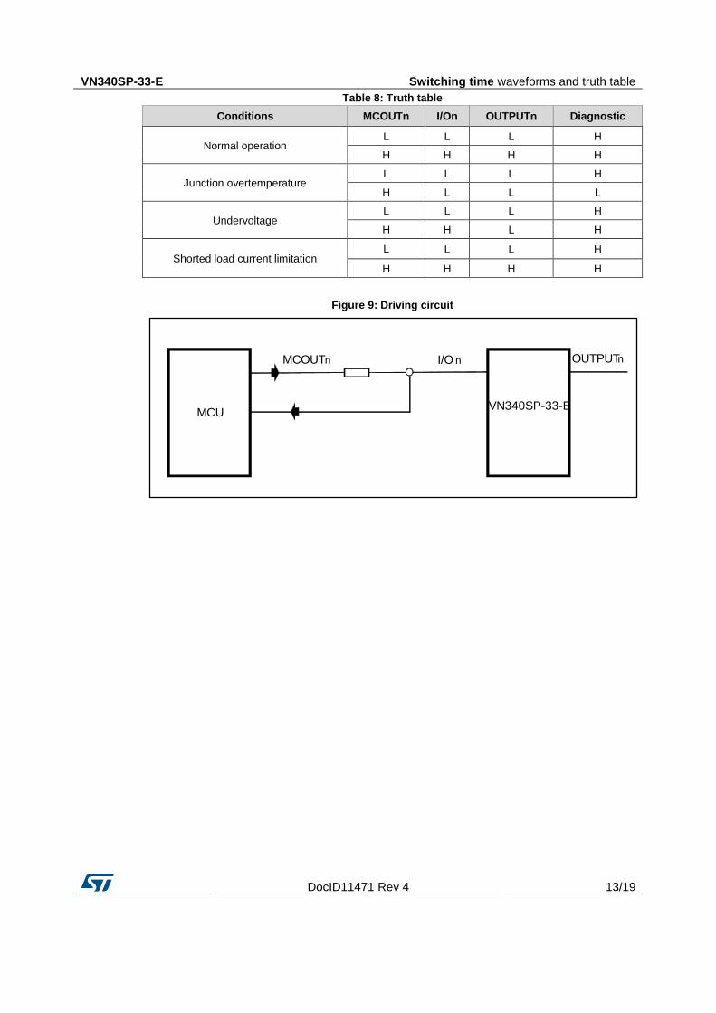
MCUVN340SP-33-E
MCOUTn I/O n OUTPUTn
Table 8: Truth table
Conditions MCOUTn I/On OUTPUTn Diagnostic
Normal operation L L L H
H H H H
Junction overtemperature L L L H
H L L L
Undervoltage L L L H
H H L H
Shorted load current limitation L L L H
H H H H
Figure 9: Driving circuit
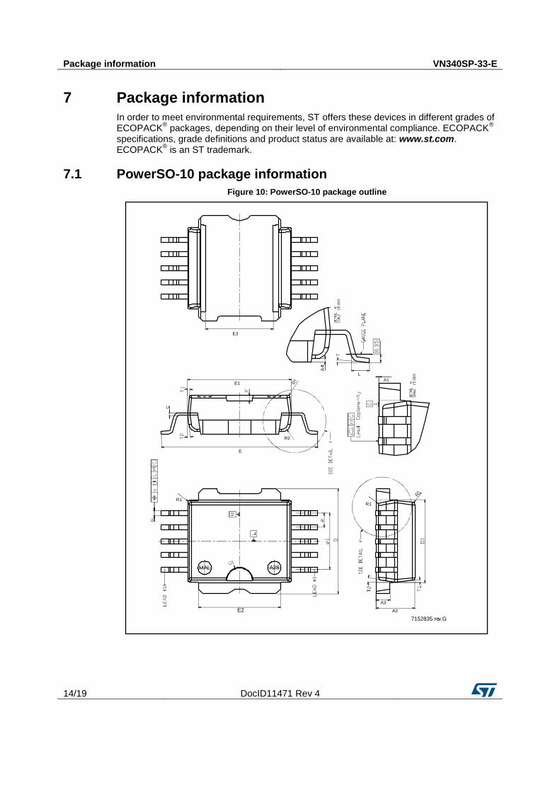
Package information VN340SP-33-E
14/19 DocID11471 Rev 4
E2
MAL A28
R1
A2
A3
L
A1
R1
E
E1
R2
E3
7152835 rev.G
7 Package information
In order to meet environmental requirements, ST offers these devices in different grades of ECOPACK
® packages, depending on their level of environmental compliance. ECOPACK
®
specifications, grade definitions and product status are available at: www.st.com. ECOPACK
® is an ST trademark.
7.1 PowerSO-10 package information
Figure 10: PowerSO-10 package outline
VN340SP-33-E Package information
DocID11471 Rev 4 15/19
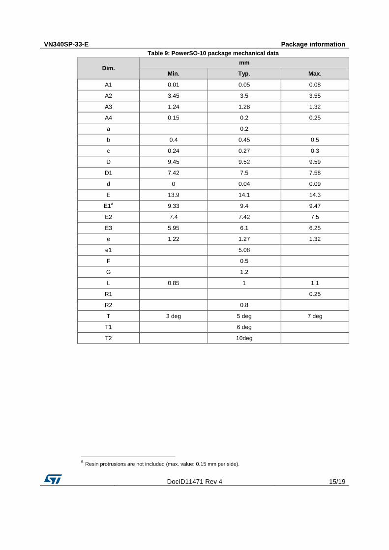
Table 9: PowerSO-10 package mechanical data
Dim. mm
Min. Typ. Max.
A1 0.01 0.05 0.08
A2 3.45 3.5 3.55
A3 1.24 1.28 1.32
A4 0.15 0.2 0.25
a
0.2
b 0.4 0.45 0.5
c 0.24 0.27 0.3
D 9.45 9.52 9.59
D1 7.42 7.5 7.58
d 0 0.04 0.09
E 13.9 14.1 14.3
E1a 9.33 9.4 9.47
E2 7.4 7.42 7.5
E3 5.95 6.1 6.25
e 1.22 1.27 1.32
e1
5.08
F
0.5
G
1.2
L 0.85 1 1.1
R1
0.25
R2
0.8
T 3 deg 5 deg 7 deg
T1
6 deg
T2
10deg
a Resin protrusions are not included (max. value: 0.15 mm per side).
Package information VN340SP-33-E
16/19 DocID11471 Rev 4
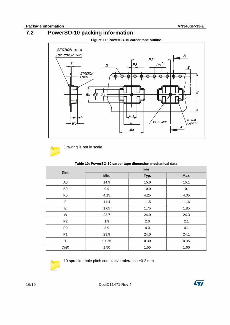
7.2 PowerSO-10 packing information
Figure 11: PowerSO-10 career tape outline
Drawing is not in scale
Table 10: PowerSO-10 career tape dimension mechanical data
Dim. mm
Min. Typ. Max.
A0 14.9 15.0 15.1
B0 9.9 10.0 10.1
K0 4.15 4.25 4.35
F 11.4 11.5 11.6
E 1.65 1.75 1.85
W 23.7 24.0 24.3
P2 1.9 2.0 2.1
P0 3.9 4.0 4.1
P1 23.9 24.0 24.1
T 0.025 0.30 0.35
D(Ø) 1.50 1.55 1.60
10 sprocket hole pitch cumulative tolerance ±0.2 mm
VN340SP-33-E Package information
DocID11471 Rev 4 17/19
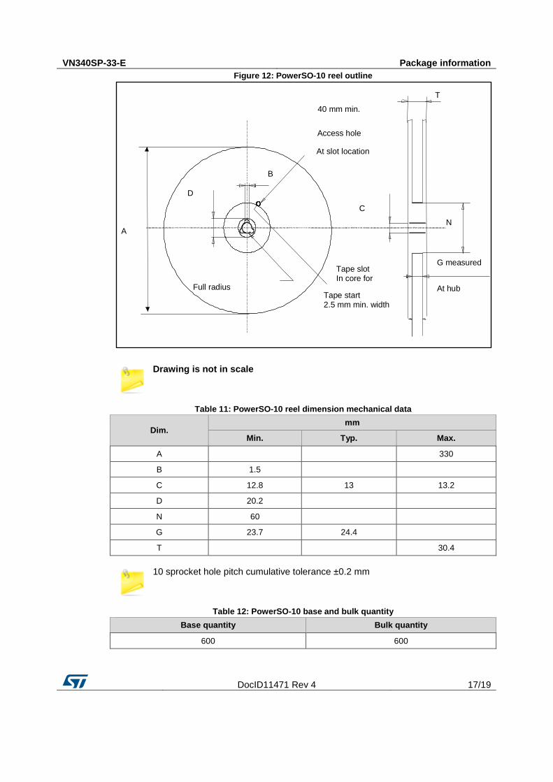
Figure 12: PowerSO-10 reel outline
Drawing is not in scale
Table 11: PowerSO-10 reel dimension mechanical data
Dim. mm
Min. Typ. Max.
A
330
B 1.5
C 12.8 13 13.2
D 20.2
N 60
G 23.7 24.4
T
30.4
10 sprocket hole pitch cumulative tolerance ±0.2 mm
Table 12: PowerSO-10 base and bulk quantity
Base quantity Bulk quantity
600 600
A
D
B
Full radius
Tape slotIn core for
Tape start2.5 mm min. width
G measured
At hub
C
N
40 mm min.
Access hole
At slot location
T
Revision history VN340SP-33-E
18/19 DocID11471 Rev 4
8 Revision history Table 13: Document revision history
Date Revision Changes
05-Sep-2005 1 Initial release.
19-Mar-2007 2 Document reformatted, typo in note 1.
22-Aug-2008 3 Updated table 9.
07-Sep-2015 4 Updated the table of absolute maximum ratings.
VN340SP-33-E
DocID11471 Rev 4 19/19
IMPORTANT NOTICE – PLEASE READ CAREFULLY
STMicroelectronics NV and its subsidiaries (“ST”) reserve the right to make changes, corrections, enhancements, modifications , and improvements to ST products and/or to this document at any time without notice. Purchasers should obtain the latest relevant information on ST products before placing orders. ST products are sold pursuant to ST’s terms and conditions of sale in place at the time of order acknowledgement.
Purchasers are solely responsible for the choice, selection, and use of ST products and ST assumes no liability for application assistance or the design of Purchasers’ products.
No license, express or implied, to any intellectual property right is granted by ST herein.
Resale of ST products with provisions different from the information set forth herein shall void any warranty granted by ST for such product.
ST and the ST logo are trademarks of ST. All other product or service names are the property of their respective owners.
Information in this document supersedes and replaces information previously supplied in any prior versions of this document.
© 2015 STMicroelectronics – All rights reserved

![Chapter 11 homework problems - gawron.sdsu.edu€¦ · John is kicked CP C C ∅ TP DP[NOM]iJohn T T[NOM]- pst VP V V is VP V V kicked DPi t S-structure John getsnominativecasechecked,](https://static.fdocument.org/doc/165x107/5ffd4740d1d48128bf1668a9/chapter-11-homework-problems-john-is-kicked-cp-c-c-a-tp-dpnomijohn-t-tnom-.jpg)