HiPerFASTTM IXGH V IGBT with Diode IXGH 24N60AU1S I · PDF fileMounting torque, TO-247 AD...
6
©1997 IXYS Corporation. All rights reserved. Symbol Test Conditions Maximum Ratings V CES T J = 25°C to 150°C 600 V V CGR T J = 25°C to 150°C; R GE = 1 MΩ 600 V V GES Continuous ±20 V V GEM Transient ±30 V I C25 T C = 25°C 48 A I C90 T C = 90°C 24 A I CM T C = 25°C, 1 ms 96 A SSOA V GE = 15 V, T VJ = 125°C, R G = 22 Ω I CM = 48 A (RBSOA) Clamped inductive load, L = 100 μH @ 0.8 V CES P C T C = 25°C 150 W T J -55 ... +150 °C T JM 150 °C T stg -55 ... +150 °C Maximum Lead and Tab temperature for soldering 300 °C 1.6 mm (0.062 in.) from case for 10 s M d Mounting torque, TO-247 AD 1.13/10 Nm/lb.in. Weight TO-247 SMD 4 g TO-247 AD 6 g Features l International standard packages JEDEC TO-247 SMD surface mountable and JEDEC TO-247 AD l IGBT and anti-parallel FRED in one package l 2nd generation HDMOS TM process l Low V CE(sat) - for minimum on-state conduction losses l MOS Gate turn-on - drive simplicity l Fast Recovery Epitaxial Diode (FRED) - soft recovery with low I RM Applications l AC motor speed control l DC servo and robot drives l DC choppers l Uninterruptible power supplies (UPS) l Switch-mode and resonant-mode power supplies Advantages l Space savings (two devices in one package) l Easy to mount with 1 screw, TO-247 (isolated mounting screw hole) l Reduces assembly time and cost Symbol Test Conditions Characteristic Values (T J = 25°C, unless otherwise specified) min. typ. max. BV CES I C = 750 μA, V GE = 0 V 600 V V GE(th) I C = 250 μA, V CE = V GE 2.5 5.5 V I CES V CE = 0.8 • V CES T J = 25°C 500 μA V GE = 0 V T J = 125°C 8 mA I GES V CE = 0 V, V GE = ±20 V ±100 nA V CE(sat) I C = I C90 , V GE = 15 V 2.7 V G C E TO-247 AD (24N60AU1) G = Gate, C = Collector, E = Emitter, TAB = Collector C (TAB) G E C (TAB) TO-247 SMD (24N60AU1S) V CES = 600 V I C25 = 48 A V CE(sat) = 2.7 V t fi = 275 ns HiPerFAST TM IGBT with Diode Combi Pack IXGH 24N60AU1 IXGH 24N60AU1S 92717H (3/97)
Transcript of HiPerFASTTM IXGH V IGBT with Diode IXGH 24N60AU1S I · PDF fileMounting torque, TO-247 AD...
©1997 IXYS Corporation. All rights reserved.
Symbol Test Conditions Maximum Ratings
VCES TJ = 25°C to 150°C 600 V
VCGR TJ = 25°C to 150°C; RGE = 1 MΩ 600 V
VGES Continuous ±20 V
VGEM Transient ±30 V
IC25 TC = 25°C 48 A
IC90 TC = 90°C 24 A
ICM TC = 25°C, 1 ms 96 A
SSOA VGE= 15 V, TVJ = 125°C, RG = 22 Ω ICM = 48 A(RBSOA) Clamped inductive load, L = 100 µH @ 0.8 VCES
PC TC = 25°C 150 W
TJ -55 ... +150 °CTJM 150 °C
Tstg -55 ... +150 °C
Maximum Lead and Tab temperature for soldering 300 °C1.6 mm (0.062 in.) from case for 10 s
Md Mounting torque, TO-247 AD 1.13/10 Nm/lb.in.
Weight TO-247 SMD 4 gTO-247 AD 6 g
Featuresl International standard packages
JEDEC TO-247 SMD surfacemountable and JEDEC TO-247 AD
l IGBT and anti-parallel FRED in onepackage
l 2nd generation HDMOSTM processl Low VCE(sat)
- for minimum on-state conductionlosses
l MOS Gate turn-on- drive simplicity
l Fast Recovery Epitaxial Diode (FRED)- soft recovery with low IRM
Applicationsl AC motor speed controll DC servo and robot drivesl DC choppersl Uninterruptible power supplies (UPS)l Switch-mode and resonant-mode
power supplies
Advantagesl Space savings (two devices in one
package)l Easy to mount with 1 screw, TO-247
(isolated mounting screw hole)l Reduces assembly time and cost
Symbol Test Conditions Characteristic Values(TJ = 25°C, unless otherwise specified)
min. typ. max.
BVCES IC = 750 µA, VGE = 0 V 600 V
VGE(th) IC = 250 µA, VCE = VGE 2.5 5.5 V
ICES VCE = 0.8 • VCES TJ = 25°C 500 µAVGE = 0 V TJ = 125°C 8 mA
IGES VCE = 0 V, VGE = ±20 V ±100 nA
VCE(sat) IC = IC90, VGE = 15 V 2.7 V
GC
E
TO-247 AD(24N60AU1)
G = Gate, C = Collector,E = Emitter, TAB = Collector
C (TAB)
GE
C (TAB)
TO-247 SMD(24N60AU1S)
VCES
= 600 VIC25
= 48 AV
CE(sat)= 2.7 V
tfi
= 275 ns
HiPerFASTTM
IGBT with DiodeCombi Pack
IXGH 24N60AU1IXGH 24N60AU1S
92717H (3/97)
IXYS MOSFETS and IGBTs are covered by one or more of the following U.S. patents: 4,835,592 4,881,106 5,017,508 5,049,961 5,187,117 5,486,7154,850,072 4,931,844 5,034,796 5,063,307 5,237,481 5,381,025
IXYS reserves the right to change limits, test conditions, and dimensions.
IXGH24N60AU1 IXGH24N60AU1S
1. Gate2. Collector
3. Emitter4. Collector
Dim. Millimeter InchesMin. Max. Min. Max.
A 4.83 5.21 .190 .205A1 2.29 2.54 .090 .100A2 1.91 2.16 .075 .085
b 1.14 1.40 .045 .055b1 1.91 2.13 .075 .084
C 0.61 0.80 .024 .031D 20.80 21.34 .819 .840
E 15.75 16.13 .620 .635e 5.45 BSC .215 BSC
L 4.90 5.10 .193 .201L1 2.70 2.90 .106 .114L2 2.10 2.30 .083 .091L3 0.00 0.10 .00 .004L4 1.90 2.10 .075 .083
ØP 3.55 3.65 .140 .144Q 5.59 6.20 .220 .244
R 4.32 4.83 .170 .190S 6.15 BSC .242 BSC
TO-247 SMD Outline
TO-247 AD Outline
Dim. Millimeter InchesMin. Max. Min. Max.
A 4.7 5.3 .185 .209A
12.2 2.54 .087 .102
A2
2.2 2.6 .059 .098
b 1.0 1.4 .040 .055b
11.65 2.13 .065 .084
b2 2.87 3.12 .113 .123C .4 .8 .016 .031D 20.80 21.46 .819 .845E 15.75 16.26 .610 .640
e 5.20 5.72 0.205 0.225L 19.81 20.32 .780 .800L1 4.50 .177
∅P 3.55 3.65 .140 .144Q 5.89 6.40 0.232 0.252
R 4.32 5.49 .170 .216S 6.15 BSC 242 BSC
e
∅ P
Symbol Test Conditions Characteristic Values(TJ = 25°C, unless otherwise specified)
min. typ. max.
gfs IC = IC90; VCE = 10 V, 9 13 SPulse test, t ≤ 300 µs, duty cycle ≤ 2 %
Cies 1500 pFCoes VCE = 25 V, VGE = 0 V, f = 1 MHz 175 pFCres 40 pF
Qg 90 120 nCQge IC = IC90, VGE = 15 V, VCE = 0.5 VCES 11 15 nCQgc 30 40 nC
td(on) 25 nstri 15 nsEon 0.6 mJtd(off) 150 200 nstfi 110 270 nsEoff 1.5 mJ
td(on) 25 nstri 15 nsEon 0.8 mJtd(off) 250 nstfi 400 nsEoff 2.3 mJ
RthJC 0.83 K/WRthCK 0.25 K/W
Inductive load, TJ = 125°°°°°C
IC = IC90, VGE = 15 V, L = 100 µH
VCE = 0.8 VCES, RG = Roff = 10 Ω
Remarks: Switching times may increasefor VCE (Clamp) > 0.8 • VCES, higher TJ orincreased RG
Inductive load, TJ = 25°°°°°C
IC = IC90, VGE = 15 V, L = 100 µH,VCE = 0.8 VCES, RG = Roff = 10 Ω
Remarks: Switching times may increasefor VCE (Clamp) > 0.8 • VCES, higher TJ orincreased RG
Min. Recommended Footprint (Dimensions in inches and (mm))
Reverse Diode (FRED) Characteristic Values(TJ = 25°C, unless otherwise specified)
Symbol Test Conditions min. typ. max.
VF IF = IC90, VGE = 0 V, 1.6 VPulse test, t ≤ 300 µs, duty cycle d ≤ 2 %
IRM IF = IC90, VGE = 0 V, -diF/dt = 240 A/µs 10 15 Atrr VR = 360 V TJ = 125°C 150 ns
IF = 1 A; -di/dt = 100 A/µs; VR = 30 VTJ = 25°C 35 50 ns
RthJC 1 K/W
©1997 IXYS Corporation. All rights reserved.
G20N60p1.JNB TJ - Degrees C
-50 -25 0 25 50 75 100 125 150
BV
/ V
GE
(th) -
Nor
mal
ized
0.6
0.7
0.8
0.9
1.0
1.1
1.2
TJ - Degrees C
-50 -25 0 25 50 75 100 125 150
VC
E(s
at) -
Nor
mal
ized
0.4
0.6
0.8
1.0
1.2
1.4
1.6
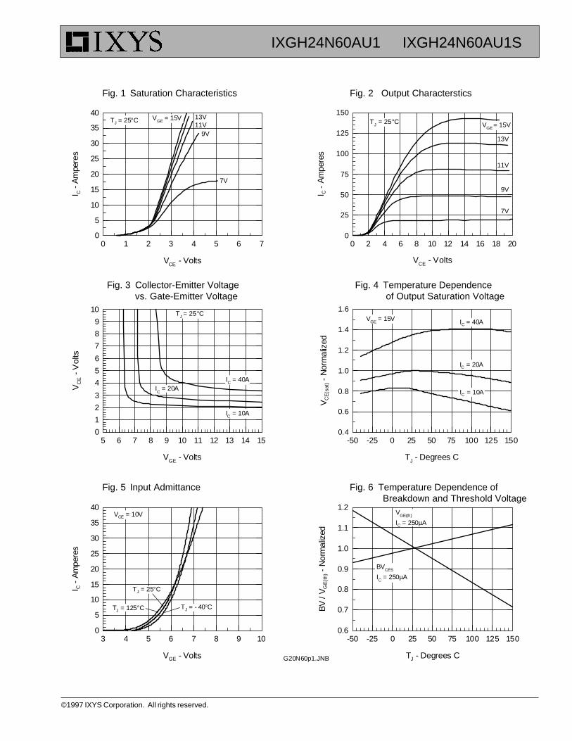
VCE - Volts
0 1 2 3 4 5 6 7
I C -
Am
pere
s
0
5
10
15
20
25
30
35
40
7V
9V
13V11V
VGE - Volts
5 6 7 8 9 10 11 12 13 14 15
VC
E -
Vol
ts
0
1
2
3
4
5
6
7
8
9
10
VGE - Volts
3 4 5 6 7 8 9 10
I C -
Am
pere
s
0
5
10
15
20
25
30
35
40
VCE - Volts
0 2 4 6 8 10 12 14 16 18 20
I C -
Am
pere
s
0
25
50
75
100
125
150
13V
11V
9V
7V
TJ = 25°C VGE = 15VVGE = 15VTJ = 25°C
IC = 10A
IC = 40AIC = 20A
TJ = 25°C
IC = 10A
IC = 20A
IC = 40AVGE = 15V
TJ = - 40°C
VCE = 10V
IC = 250µA
IC = 250µA
VGE(th)
BVCES
TJ = 25°C
TJ = 125°C
Fig. 3 Collector-Emitter Voltage Fig. 4 Temperature Dependencevs. Gate-Emitter Voltage of Output Saturation Voltage
Fig. 5 Input Admittance Fig. 6 Temperature Dependence of Breakdown and Threshold Voltage
Fig. 1 Saturation Characteristics Fig. 2 Output Characterstics
IXGH24N60AU1 IXGH24N60AU1S
IXYS MOSFETS and IGBTs are covered by one or more of the following U.S. patents: 4,835,592 4,881,106 5,017,508 5,049,961 5,187,117 5,486,7154,850,072 4,931,844 5,034,796 5,063,307 5,237,481 5,381,025
IXYS reserves the right to change limits, test conditions, and dimensions.
IXGH24N60AU1 IXGH24N60AU1S
Pulse Width - seconds
0.0001 0.001 0.01 0.1 1 10
Zth
jc (K
/W)
0.01
0.1
1
D=0.1
D=0.2
D=0.5
VCE - Volts
0 100 200 300 400 500 600
I C -
Am
pere
s
0.01
0.1
1
10
100
Qg - nanocoulombs
0 25 50 75 100
VG
E -
Vol
ts
0
3
6
9
12
15IC = 24A
VCE = 300V
RG - Ohms
0 20 40 60 80 100 120
Eof
f - m
illijo
ules
0
1
2
3
4
5
t fi - n
anos
econ
ds
0
100
200
300
400
500
Eoff
tfi
IC - Amperes
0 10 20 30 40 50E
off -
mill
ijoul
es
0
1
2
3
4
5
t fi - n
anos
econ
ds
0
100
200
300
400
500Eoff
tfi
TJ = 125°C
RG = 10ΩTJ = 125°C
IC = 24A
TJ = 125°C
RG = 10Ω
D=0.05
D=0.02
Single PulseD=0.01
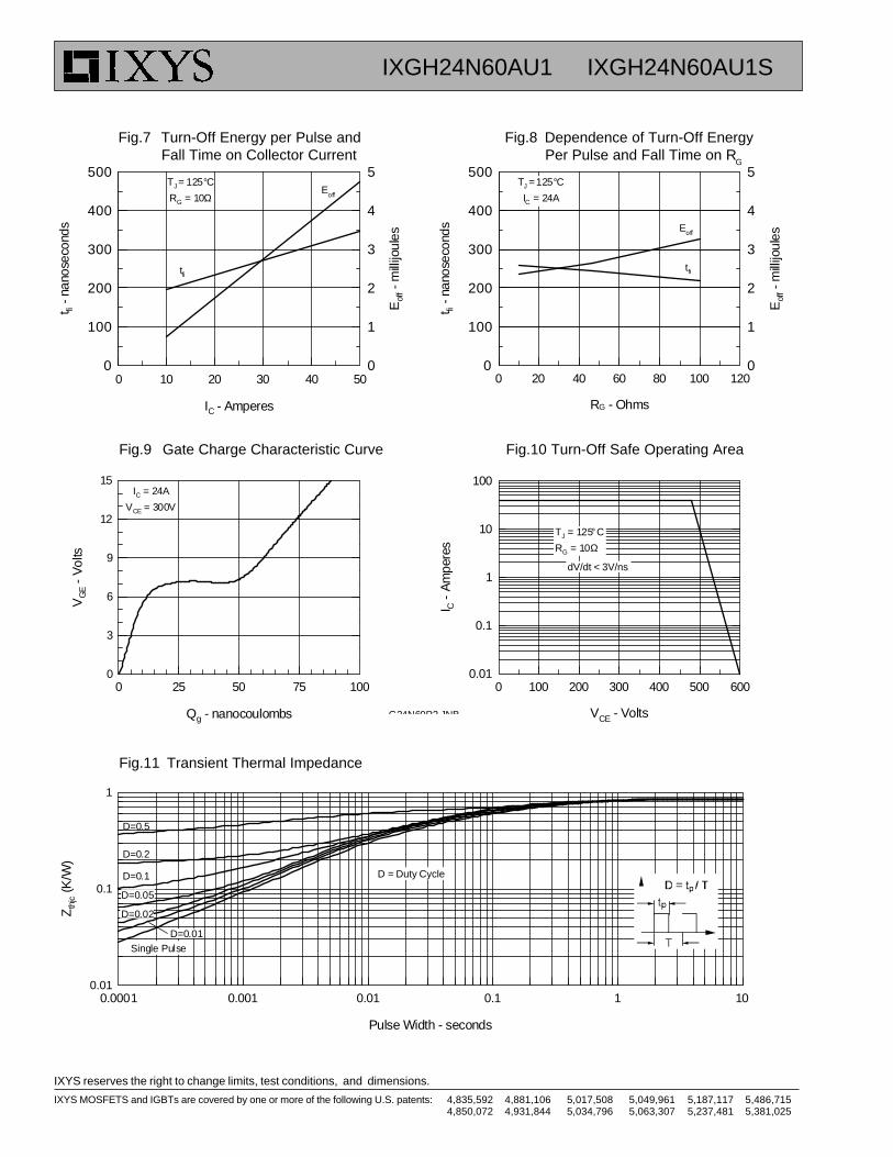
G24N60P2.JNB
D = Duty Cycle
Fig.11 Transient Thermal Impedance
Fig.9 Gate Charge Characteristic Curve Fig.10 Turn-Off Safe Operating Area
Fig.7 Turn-Off Energy per Pulse and Fig.8 Dependence of Turn-Off EnergyFall Time on Collector Current Per Pulse and Fall Time on R
G
dV/dt < 3V/ns
©1997 IXYS Corporation. All rights reserved.
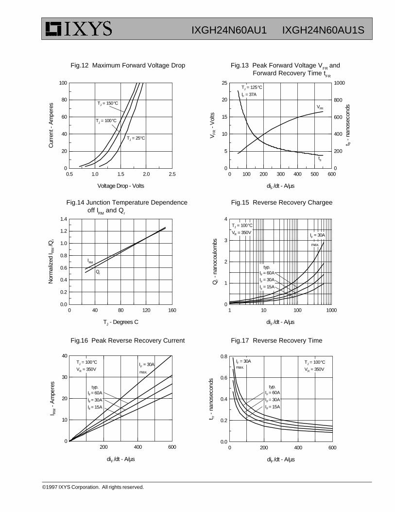
Fig.16 Peak Reverse Recovery Current Fig.17 Reverse Recovery Time
diF /dt - A/µs
0 200 400 600
t rr -
nano
seco
nds
0.0
0.2
0.4
0.6
0.8
diF /dt - A/µs
200 400 600
I RM -
Am
pere
s
0
10
20
30
40
diF /dt - A/µs
1 10 100 1000
Qr -
nan
ocou
lom
bs
0
1
2
3
4
TJ - Degrees C
0 40 80 120 160
Nor
mal
ized
I RM
/Qr
0.0
0.2
0.4
0.6
0.8
1.0
1.2
1.4
Qr
IRM
diF /dt - A/µs
0 100 200 300 400 500 600
t fr -
nano
seco
nds
0
200
400
600
800
1000
VF
R -
Vol
ts
0
5
10
15
20
25
tfr
VFR
Voltage Drop - Volts
0.5 1.0 1.5 2.0 2.5
Cur
rent
- A
mpe
res
0
20
40
60
80
100
TJ = 150°C
TJ = 100°C
TJ = 25°C
TJ = 125°C
IF = 37A
typ.IF = 60A
IF = 30A
IF = 15A
IF = 30A
TJ = 100°C
VR = 350V
TJ = 100°C
VR = 350V
TJ = 100°C
VR = 350V
typ.IF = 60A
IF = 30A
IF = 15A
max.
IF = 30Amax.
IF = 30A
typ.IF = 60A
IF = 30A
IF = 15A
max.
Fig.12 Maximum Forward Voltage Drop Fig.13 Peak Forward Voltage VFR
and Forward Recovery Time t
FR
Fig.14 Junction Temperature Dependence Fig.15 Reverse Recovery Chargee off I
RM and Q
r
IXGH24N60AU1 IXGH24N60AU1S
IXYS MOSFETS and IGBTs are covered by one or more of the following U.S. patents: 4,835,592 4,881,106 5,017,508 5,049,961 5,187,117 5,486,7154,850,072 4,931,844 5,034,796 5,063,307 5,237,481 5,381,025
IXYS reserves the right to change limits, test conditions, and dimensions.
IXGH24N60AU1 IXGH24N60AU1S
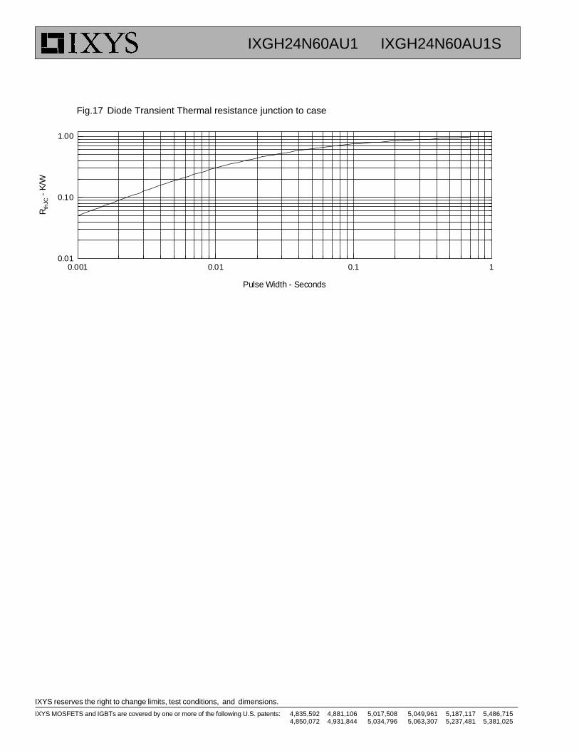
Pulse Width - Seconds
0.001 0.01 0.1 1
Rth
JC -
K/W
0.01
0.10
1.00
Fig.17 Diode Transient Thermal resistance junction to case