
IRPT1060 - Semiconductor & System Solutions - Infineon … · · 1998-09-21control system...
12
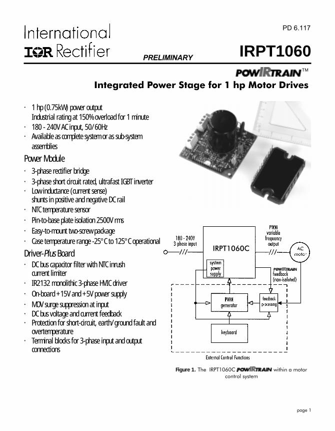
page 1 PD 6.117 ΤΜ Integrated Power Stage for 1 hp Motor Drives IRPT1060 PRELIMINARY · 1 hp (0.75kW) power output Industrial rating at 150% overload for 1 minute · 180 - 240V AC input, 50/60Hz · Available as complete system or as sub-system assemblies Power Module · 3-phase rectifier bridge · 3-phase short circuit rated, ultrafast IGBT inverter · Low inductance (current sense) shunts in positive and negative DC rail · NTC temperature sensor · Pin-to-base plate isolation 2500V rms · Easy-to-mount two-screw package · Case temperature range -25°C to 125°C operational Driver-Plus Board · DC bus capacitor filter with NTC inrush current limiter · IR2132 monolithic 3-phase HVIC driver · On-board +15V and +5V power supply · MOV surge suppression at input · DC bus voltage and current feedback · Protection for short-circuit, earth/ground fault and overtemperature · Terminal blocks for 3-phase input and output connections Figure 1. The IRPT1060C within a motor control system IRPT1060C
Transcript of IRPT1060 - Semiconductor & System Solutions - Infineon … · · 1998-09-21control system...
page 1
PD 6.117
ΤΜ
Integrated Power Stage for 1 hp Motor Drives
IRPT1060PRELIMINARY
· 1 hp (0.75kW) power outputIndustrial rating at 150% overload for 1 minute
· 180 - 240V AC input, 50/60Hz· Available as complete system or as sub-system
assemblies
Power Module· 3-phase rectifier bridge· 3-phase short circuit rated, ultrafast IGBT inverter· Low inductance (current sense)
shunts in positive and negative DC rail· NTC temperature sensor· Pin-to-base plate isolation 2500V rms· Easy-to-mount two-screw package· Case temperature range -25°C to 125°C operational
Driver-Plus Board· DC bus capacitor filter with NTC inrush
current limiter· IR2132 monolithic 3-phase HVIC driver· On-board +15V and +5V power supply· MOV surge suppression at input· DC bus voltage and current feedback· Protection for short-circuit, earth/ground fault and
overtemperature· Terminal blocks for 3-phase input and output
connections
Figure 1. The IRPT1060C within a motorcontrol system
IRPT1060C
IRPT1060
page 2
The IRPT1060C provides the completeconversion function for a 1hp (0.75kW) variable frequency,variable voltage, AC motor controller. The combines a power module IRPT1060A with a Driver-Plus BoardIRPT1060D. Figure 1 shows the block diagram of the
within an AC motor control system.The power module contains a 3-phase input bridge rectifier,
3-phase IGBT inverter, current sense shunts, and a thermistor. Itis designed for easy mounting to a heat sink. The Driver-PlusBoard contains DC link capacitors, capacitor soft charge functionusing NTC thermistor, surge suppression MOVs, IGBT gatedrivers, DC bus voltage and current feedback signals, protetioncircuitry and local power supply. It is designed to mate with acontroller board through a single row header. Terminal blocks areprovided on the Driver-Plus Board for all end user line input andmotor output.
Output power is Pulse-Width Modulated (PWM) 3-phase,variable frequency, variable voltage controlled by an externallygenerated user-provided PWM controller for inverter IGBTswitching. The power supply offers the user non-isolated 5V and15V to power the micro-controller.
The IRPT1060C offers several benefits to the drivemanufacturer listed below:• It greatly simplifies component selection, design of layout,
interconnection, gate drive, local power supply, thermalsensing, current sensing and protection.
• Gate drive and protection circuits are designed to closelymatch the operating characteristics of the powersemiconductors. This allows power losses to be minimized andpower rating to be maximized to a greater extent than ispossible by designing with individual components.
• It reduces the effort of calculating and evaluating powersemiconductor losses and junction temperature.
• It reduces the manufacturer's part inventory and simplifiesassembly.[ specifications and ratings are given for system
input and output voltage and current, power losses and heat sinkrequirements over a range of operating conditions.
system ratings are verified by IR in final testing.]
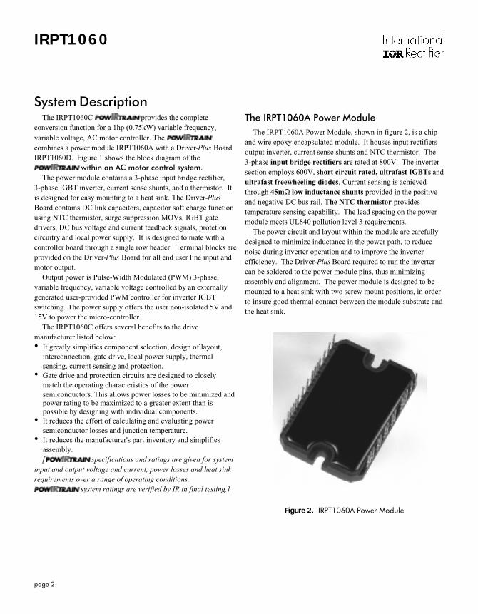
The IRPT1060A Power ModuleThe IRPT1060A Power Module, shown in figure 2, is a chip
and wire epoxy encapsulated module. It houses input rectifiersoutput inverter, current sense shunts and NTC thermistor. The3-phase input bridge rectifiers are rated at 800V. The invertersection employs 600V, short circuit rated, ultrafast IGBTs andultrafast freewheeling diodes. Current sensing is achievedthrough 45mΩ low inductance shunts provided in the positiveand negative DC bus rail. The NTC thermistor providestemperature sensing capability. The lead spacing on the powermodule meets UL840 pollution level 3 requirements.
The power circuit and layout within the module are carefullydesigned to minimize inductance in the power path, to reducenoise during inverter operation and to improve the inverterefficiency. The Driver-Plus Board required to run the invertercan be soldered to the power module pins, thus minimizingassembly and alignment. The power module is designed to bemounted to a heat sink with two screw mount positions, in orderto insure good thermal contact between the module substrate andthe heat sink.
System Description
Figure 2. IRPT1060A Power Module
IRPT1060
page 3
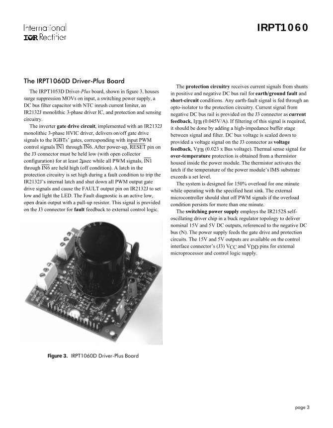
Figure 3. IRPT1060D Driver-Plus Board
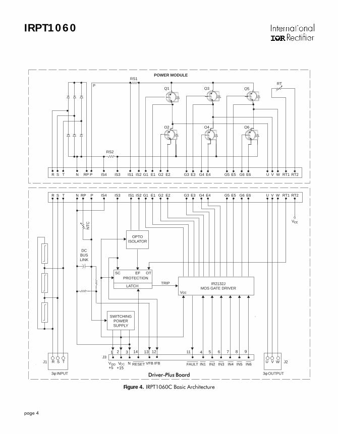
The protection circuitry receives current signals from shuntsin positive and negative DC bus rail for earth/ground fault andshort-circuit conditions. Any earth-fault signal is fed through anopto-isolator to the protection circuitry. Current signal fromnegative DC bus rail is provided on the J3 connector as currentfeedback, IFB (0.045V/A). If filtering of this signal is required,it should be done by adding a high-impedance buffer stagebetween signal and filter. DC bus voltage is scaled down toprovided a voltage signal on the J3 connector as voltagefeedback, VFB (0.023 x Bus voltage). Thermal sense signal forover-temperature protection is obtained from a thermistorhoused inside the power module. The thermistor activates thelatch if the temperature of the power module’s IMS substrateexceeds a set level.
The system is designed for 150% overload for one minutewhile operating with the specified heat sink. The externalmicrocontroller should shut off PWM signals if the overloadcondition persists for more than one minute.
The switching power supply employs the IR2152S self-oscillating driver chip in a buck regulator topology to delivernominal 15V and 5V DC outputs, referenced to the negative DCbus (N). The power supply feeds the gate drive and protectioncircuits. The 15V and 5V outputs are available on the controlinterface connector’s (J3) VCC and VDD pins for externalmicroprocessor and control logic supply.
The IRPT1060D Driver-Plus Board
The IRPT1053D Driver-Plus board, shown in figure 3, housessurge suppression MOVs on input, a switching power supply, aDC bus filter capacitor with NTC inrush current limiter, anIR2132J monolithic 3-phase driver IC, and protection and sensingcircuitry.
The inverter gate drive circuit, implemented with an IR2132Jmonolithic 3-phase HVIC driver, delivers on/off gate drivesignals to the IGBTs’ gates, corresponding with input PWMcontrol signals IN1 through IN6. After power-up, RESET pin onthe J3 connector must be held low (with open collectorconfiguration) for at least 2µsec while all PWM signals, IN1through IN6 are held high (off condition). A latch in theprotection circuitry is set high during a fault condition to trip theIR2132J’s internal latch and shut down all PWM output gatedrive signals and cause the FAULT output pin on IR2132J to setlow and light the LED. The Fault diagnostic is an active low,open drain output with a pull-up resistor. This signal is providedon the J3 connector for fault feedback to external control logic.
IRPT1060
page 4
Figure 4. IRPT1060C Basic Architecture
IS1IS4 IS3
IS4 IS3
RS1
RS2
Q1 Q3 Q5
Q2 Q4 Q6
RTP
IS2 G1 E1R S T N RP P
R S T N RP P
G2 E2 G3 E3 G4 E4 G5 E5 G6 E6 U V W RT1 RT2
IS1 IS2 G1 E1 G2 E2 G3 E3 G4 E4 G5 E5 G6 E6
UIN6
V W
RT1WVU RT2
V
R SJ1J3
J2
3φ OUTPUT3φ INPUT
TIN5IN4IN3
IR2132JMOS GATE DRIVER
PROTECTION
LATCH
NT
C
TRIP
OPTOISOLATOR
SWITCHINGPOWERSUPPLY
DCBUSLINK
IN2
SC EF OT
IN1IFBVFBN FAULTRESETV
Vcc
cc
CCDD V
21 3 14 13 12 11 4 5 6 7 8 9
DRIVER BOARD PLUS
POWER MODULE
+5 +15
Driver-Plus Board
IRPT1060
page 5
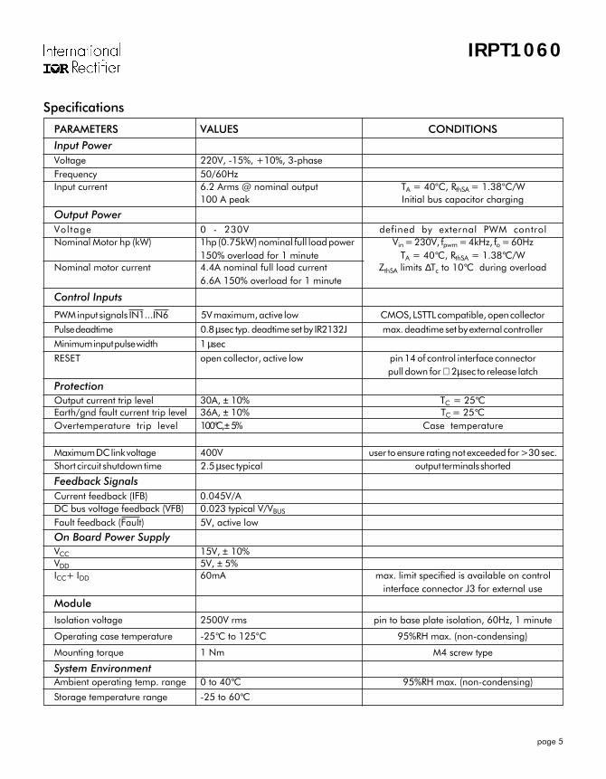
Specifications
PARAMETERS VALUES CONDITIONS
Input PowerVoltage 220V, -15%, +10%, 3-phaseFrequency 50/60HzInput current 6.2 Arms @ nominal output TA = 40°C, RthSA = 1.38°C/W
100 A peak Initial bus capacitor charging
Output PowerVoltage 0 - 230V defined by external PWM controlNominal Motor hp (kW) 1hp (0.75kW) nominal full load power Vin = 230V, fpwm = 4kHz, fo = 60Hz
150% overload for 1 minute TA = 40°C, RthSA = 1.38°C/WNominal motor current 4.4A nominal full load current ZthSA limits ∆Tc to 10°C during overload
6.6A 150% overload for 1 minute
Control Inputs
PWM input signals IN1...IN6 5V maximum, active low CMOS, LSTTL compatible, open collector
Pulse deadtime 0.8 µsec typ. deadtime set by IR2132J max. deadtime set by external controller
Minimum input pulse width 1 µsec
RESET open collector, active low pin 14 of control interface connectorpull down for ⊕ 2µsec to release latch
ProtectionOutput current trip level 30A, ± 10% TC = 25°CEarth/gnd fault current trip level 36A, ± 10% TC = 25°COvertemperature trip level 100°C, ± 5% Case temperature
Maximum DC link voltage 400V user to ensure rating not exceeded for >30 sec.Short circuit shutdown time 2.5 µsec typical output terminals shorted
Feedback SignalsCurrent feedback (IFB) 0.045V/ADC bus voltage feedback (VFB) 0.023 typical V/VBUS
Fault feedback (Fault) 5V, active low
On Board Power SupplyVCC 15V, ± 10%VDD 5V, ± 5%ICC+ IDD 60mA max. limit specified is available on control
interface connector J3 for external use
Module
Isolation voltage 2500V rms pin to base plate isolation, 60Hz, 1 minute
Operating case temperature -25°C to 125°C 95%RH max. (non-condensing)
Mounting torque 1 Nm M4 screw type
System EnvironmentAmbient operating temp. range 0 to 40°C 95%RH max. (non-condensing)
Storage temperature range -25 to 60°C
IRPT1060
page 6
0
0.5
1
1 .5
2
2 .5
1 4 8 1 2 1 6 2 0 2 40
1 0
2 0
3 0
4 0
5 0
6 0
7 0
0
0.2
0 .4
0 .6
0 .8
1
1 .2
1 .4
1 .6
1 .8
2
1 4 8 1 2 1 6 2 0 2 40
1 0
2 0
3 0
4 0
5 0
6 0
7 0
8 0
9 0
Power100%
Power150%
RthSA 150% load(1 min.) Down to 3 Hz
RthSA 150% load(1 min.) 10-60 Hz
0.75 hp(0.56 kW)
RthSA 100% load continuous10-60 Hz
Power100%
Power150%
RthSA 150% load(1 min.) down to 3 Hz
RthSA 150% load(1 min.) 10-60 Hz
1.0 hp(0.75 kW)
RthSA 100% load continuous10-60 Hz
Tota
l Pow
er D
issi
patio
n (W
atts)
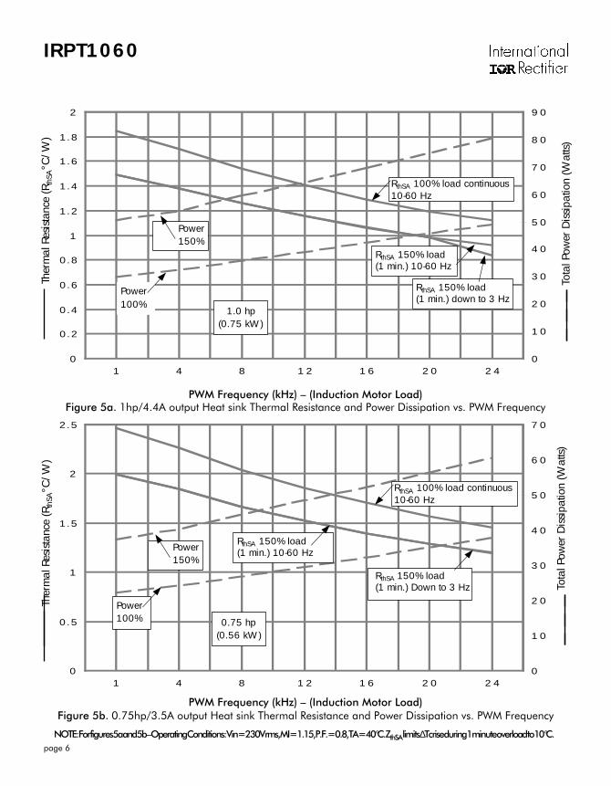
PWM Frequency (kHz) – (Induction Motor Load)Figure 5b. 0.75hp/3.5A output Heat sink Thermal Resistance and Power Dissipation vs. PWM Frequency
NOTE: For figures 5a and 5b – Operating Conditions: Vin = 230V rms, MI = 1.15, P.F. = 0.8, TA = 40°C. ZthSA limits ∆Tc rise during 1 minute overload to 10°C.
PWM Frequency (kHz) – (Induction Motor Load)Figure 5a. 1hp/4.4A output Heat sink Thermal Resistance and Power Dissipation vs. PWM Frequency
Tota
l Pow
er D
issi
patio
n (W
atts)
Ther
mal
Res
ista
nce
(Rth
SA°C
/W)
Ther
mal
Res
ista
nce
(Rth
SA°C
/W)
IRPT1060
page 7
Mounting, Hookup and Application Instructions
Mounting1. Remove all particles and grit from the heat sink and power
substrate.2. Spread a .004" to .005" layer of silicone grease on the heat
sink, covering the entire area that the power substrate willoccupy. Recommended heat sink flatners is .001 inch/inch andTotal Indicator Readout (TIR) of .003 inch below substrate
3. Place the power substrate onto the heat sink with themounting holes aligned and press it firmly into the siliconegrease.
4. Place the 2 M4 mounting screws through the PCB andpower module and into the heat sink and tighten the screws to 1Nm torque.
Control ConnectionsAll input and output control connections are made via a 16-
terminal female connector to J3.
Power Connections3-phase input connections are made to terminals R,S and T
(J1). Inverter output terminal connections are made to terminalsU,V and W (J2).
Power-Up ProcedureWhen 3-phase input power is first switched on, PWM inputs
to the IRPT1053C must be inhibited (held high) until theprotection latch circuitry is reset. To reset this latch beforeinverter start-up, RESET pin on J3 connector must be pulleddown low for at least 2 µsec. This will set the Fault feedbacksignal on J3 high. Now, the PWM input signals can be appliedfor inverter start-up.
Power-Down ProcedureThe following sequence is recommended for normal power
down:1. reduce motor speed by PWM control2. inhibit PWM inputs3. disconnect main power.
123456789012345678901234567890123456789012345678901234567890123456789012345678901234567890123456789012345678901234567890123456789012345678901234567890123456789012345678901234567890123456789012345678901234567890123456789012345678901234567890123456789012345678901234567890123456789012345678901234567890123456789012345678901234567890123456789012345678901234567890123456789012345678901234567890123456789012345678901234567890123456789012345678901234567890
1 2
Figure 7a. Control Signal Connector Figure 7b. Input and Output Terminal Blocks
Figure 6. Power Module Mounting Screw Sequence
IRPT1060
page 8
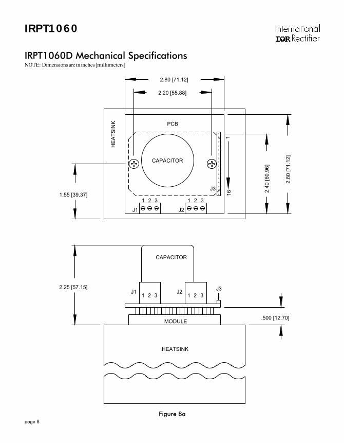
NOTE: Dimensions are in inches [milliimeters]
IRPT1060D Mechanical Specifications
2.4
0 [
60
.96
]
.500 [12.70]
1.55 [39.37]
J332132
321321
1
2.25 [57.15]
2.80 [71.12]
2.20 [55.88]
PCB
CAPACITOR
11
6J3
J2J1
HE
AT
SIN
K
HEATSINK
MODULE
CAPACITOR
J2J12
.80
[7
1.1
2]
Figure 8a
IRPT1060
page 9
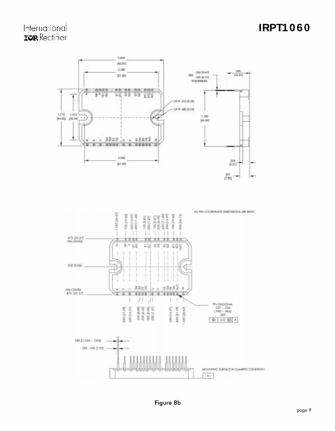
Figure 8b

IRPT1060
page 10
Part Number Identification and Ordering Instructions
IRPT1060A Power ModuleChip and wire epoxy encapsulated module with 800V
rectifiers, 600V short-circuit rated, ultra-fast IGBT inverter withultra-fast freewheeling diodes, temperature sensing NTCthermistor and current-sensing low-inductance shunts.
IRPT1060C Integrated Power Module (IRPT1060A) and Driver-Plus
Board (IRPT1060D) pre-assembled and tested to meet all systemspecifications.
IRPT1060D Driver-Plus BoardPrinted Circuit board assembled with DC link capacitors, NTC
in-rush limiting thermistor, high-power terminal blocks, surgesuppression MOVs, IGBT gate drivers, protection circuitry andlow power supply. The PCB is functionally tested with standardpower module to meet all system specifications.
IRPT1060E Design KitComplete (IRPT1060C) with full set of design
documentation including schematic diagram, bill of material,mechanical layout, schematic files, Gerber files and design tips.
IRPT1060
page 11
Earth/ground fault from positive bus to earth is detected bythe shunt in the postive bus and an opto-coupler. When faultcurrent exceeds a nominal value of 36A, this protection isactivated.
Overtemperature is measured by a thermistor mounted closeto the inverter section. When the substrate temperature exceeds anominal value of 100°C, this protection is activated.
If any of the protection features is activated, the TRIP signalgoes high and is latched high, activating the internal latch inIR2132J, which turns all gates to the inverter section off,acknowledging to the controller through FAULT and turns on theLED.
Trip Reset
The internal latch of the IR2132J can be reset by holding IN2,IN4 and IN6 OFF simultaneously for a period greater than 12 µs.The TRIP signal can be removed by pulling down the RESETpin through the open collector device for 2µs, this should bedone only after IN1,...,IN6 are turned OFF.
Interface with system controller
All signals are referred to negative DC bus (N). IN1,...IN6 areTTL/CMOS compatible active low signals. Maximum voltagerating for these signals is 5V. All channels are provided withpull-up resistors and can be used with open collector inputs aswell.
FAULT is open collector, active low signal, provided with47K pull-up resistor. Typical current sink capacity for this pin is5 mA.
RESET should be applied with open collector device only andonly after IN1,...IN6 are turned OFF. Recommended RESETpulse duration is 2µs.
VDD is 5V and VCC is 15V output. If 5V output is used with alarge external capacitor, a diode should be connected betweenVDD (anode) and VCC (cathode) to ensure that VDD does notexceed VCC, due to potentially different discharge times forstorage capacitors when power is turned OFF.
VFB is scaled down dc bus voltage (0.023 X Vbus nominal).
Functional Information
CAUTION:All control logic is referenced to negative power
bus which is live with respect to earth/ground.
Capacitor Soft Charge
A DC bus capacitor is connected to the rectifier bridge outputthrough an NTC. At power-up, the NTC limits the inrush currentto 100A. During normal operation current through the NTCreduces its resistance, hence reducing its losses.
System Power Supply
A buck converter designed with IR2152 and operating fromthe dc bus generates VCC (15V) and VDD(5V) for drive andprotection circuits. Both VCC and VDD are available at thecontrol connector to supply microprocessor controls. Totalcurrent available from VCC and VDD (ICC and ID, respectively) is60mA for external use.
Floating power supplies for high side devices are derivedthrough bootstrap technique, simplifying power supplyrequirements.
Gate Drive Circuits
Gate drive for the inverter is implemented with an IR2132Jmonolithic 3-phase HVIC driver. Short circuit buffer powersupply counters the voltage drop across a shunt in the negative dcbus, allowing the device to have nominal gate voltage duringshort circuit and maintaining short circuit current to a detectablelevel.
The undervoltage circuit monitors the local gate driver powersupply voltage and sends a high input signal duringundervoltage, setting the latch and inhibiting the PWM inputsignals.
System Protections
Short circuit is monitored through a shunt in the negativebus, which detects phase-to-phase short circuits and phase-to-earth short circuits (when current flows from earth to negativebus). Voltage drop across the shunt is compared to a pre-set limitand when the current exceeds a nominal value of 30A thisprotection is activated.
IRPT1060
page 12
IFB is DC bus current, 0.045V/A nominal. This pin must not beconnected to circuit ground (N) through low impedance. Iffiltering of this signal is required, it shoud be done by adding ahigh impedance buffer stage between signal and filter.
Heat sink Requirements
Figures 5a and 5b of the IRPT1053 datasheet show thethermal resistance of the heat sink required for various outputpower levels and PWM switching frequencies. Maximum totallosses of the unit are also shown.
This data is based on the following key operating conditions:• The maximum continuous combined losses of the rectifier
and inverter occur at full pulse-width-modulation. Thesemaximum losses set the maximum continuous operatingtemperature of the heat sink.
• The maximum combined losses of the rectifier andinverter at full pulse-width modulation under overload set
WORLD HEADQUARTERS: 233 Kansas St., El Segundo, California 90245, Tel: (310) 322 3331EUROPEAN HEADQUARTERS: Hurst Green, Oxted, Surrey RH8 9BB, UK Tel: ++ 44 1883 732020
IR CANADA: 7321 Victoria Park Ave., Suite 201, Markham, Ontario L3R 2Z8, Tel: (905) 475 1897IR GERMANY: Saalburgstrasse 157, 61350 Bad Homburg Tel: ++ 49 6172 96590
IR ITALY: Via Liguria 49, 10071 Borgaro, Torino Tel: ++ 39 11 451 0111IR FAR EAST: 171 (K&H Bldg.), 30-4 Nishi-ikebukuro 3-Chome, Toshima-ku, Tokyo Japan Tel: 81 3 3983 0086IR SOUTHEAST ASIA: 315 Outram Road, #10-02 Tan Boon Liat Building, Singapore 0316 Tel: 65 221 8371
http://www.irf.com/ Data and specifications subject to change without notice. 9/97
the incremental temperature rise of the heat sink duringoverload, which is limited to 10°C due to ZthSA.
• The minimum output frequency at which full overloadcurrent is to be delivered sets the peak IGBT junctiontemperatures.
• At low output frequency IGBT junction temperature tendsto follow the instantaneous fluctuations of the outputcurrent. Thus, peak junction temperature rise increases asoutput frequency decreases.
Voltage Rise During Braking
The motor will feed energy back to the DC link during electricbraking, forcing DC bus voltage to rise above the level definedby input line voltage. Deceleration of the motor must becontrolled by appropriate PWM control to keep the DC busvoltage within the rated maximum value.