Datasheet - renesas.com · 4. θJA is measured with the component mounted on a low-effective...
22
FN6040 Rev.2.00 Page 1 of 22 Apr.19.19 ISL83387E ±15kV ESD Protected, +3V to +5.5V, 1Microamp, 250kbps, RS-232 Transceivers with Enhanced Automatic Powerdown Datasheet The ISL83387E is a 3.0V to 5.5V powered RS-232 transceiver that meets ElA/TIA-232 and V.28/V.24 specifications, even at V CC = 3.0V. Additionally, it provides ±15kV ESD protection (IEC61000-4-2 Air Gap and Human Body Model) on transmitter outputs and receiver inputs (RS-232 pins). Targeted applications are industrial laptop computers, Palmtops, PDAs, and notebooks where the low operational power consumption and even lower standby power consumption is critical. Efficient on-chip charge pumps coupled with manual and enhanced automatic powerdown functions reduce the standby supply current to a 1µA trickle. The TSSOP packaging and the use of small, low value capacitors ensure board space savings. Data rates greater than 250kbps are ensured at worst case load conditions. The ISL83387E features a V L pin that adjusts the logic pin output levels and input thresholds to values compatible with the V CC powering the external logic (for example, a UART). The ISL83387E includes an enhanced automatic power-down function that powers down the on-chip power-supply and driver circuits. Automatic powerdown occurs when all receiver and transmitter inputs detect no signal transitions for a period of 30 seconds. The ISL83387E powers back up automatically, when it senses a transition on any transmitter or receiver input. Table 1 summarizes the features of the ISL83387E and Application Note AN9863 summarizes the features of each device comprising the 3V RS-232 family. Related Literature For a full list of related documents, visit our website: • ISL83387E device page Features •V L supply pin for compatibility with mixed voltage systems • ESD protection for RS-232 I/O pins to ±15kV (IEC61000) • Low power, pin compatible upgrade for MAX3387E • Manual and enhanced automatic powerdown features • Meets EIA/TIA-232 and V.28/V.24 specifications at 3V • On-chip charge pumps require only four external 0.1µF capacitors • Receivers stay active in powerdown • Very low supply current: 300µA • Assured minimum data rate: 250kbps • Wide power supply range: Single +3V to +5.5V • Low supply current in powerdown state: < 1µA • Pb-Free (RoHS compliant) Applications • Any system requiring RS-232 communication ports ○ Battery powered, hand-held, and portable equipment ○ Industrial laptops. Palmtops, and PDAs ○ Digital cameras Table 1. Summary of Features Part Number No. of Tx. No. of Rx. Data Rate (kbps) Rx. Enable Function? V L Logic Supply Pin? Manual Power-Down? Enhanced Automatic Powerdown Function? ISL83387E 3 3 250 No Yes Yes Yes
-
Upload
truongcong -
Category
Documents
-
view
214 -
download
0
Transcript of Datasheet - renesas.com · 4. θJA is measured with the component mounted on a low-effective...

FN6040 Rev.2.00 Page 1 of 22Apr.19.19
ISL83387E±15kV ESD Protected, +3V to +5.5V, 1Microamp, 250kbps, RS-232 Transceivers with Enhanced Automatic Powerdown
Datasheet
The ISL83387E is a 3.0V to 5.5V powered RS-232 transceiver that meets ElA/TIA-232 and V.28/V.24 specifications, even at VCC = 3.0V. Additionally, it provides ±15kV ESD protection (IEC61000-4-2 Air Gap and Human Body Model) on transmitter outputs and receiver inputs (RS-232 pins). Targeted applications are industrial laptop computers, Palmtops, PDAs, and notebooks where the low operational power consumption and even lower standby power consumption is critical. Efficient on-chip charge pumps coupled with manual and enhanced automatic powerdown functions reduce the standby supply current to a 1µA trickle. The TSSOP packaging and the use of small, low value capacitors ensure board space savings. Data rates greater than 250kbps are ensured at worst case load conditions.
The ISL83387E features a VL pin that adjusts the logic pin output levels and input thresholds to values compatible with the VCC powering the external logic (for example, a UART).
The ISL83387E includes an enhanced automatic power-down function that powers down the on-chip power-supply and driver circuits. Automatic powerdown occurs when all receiver and transmitter inputs detect no signal transitions for a period of 30 seconds. The ISL83387E powers back up automatically, when it senses a transition on any transmitter or receiver input.
Table 1 summarizes the features of the ISL83387E and Application Note AN9863 summarizes the features of each device comprising the 3V RS-232 family.
Related Literature
For a full list of related documents, visit our website:
• ISL83387E device page
Features
• VL supply pin for compatibility with mixed voltage systems
• ESD protection for RS-232 I/O pins to ±15kV (IEC61000)
• Low power, pin compatible upgrade for MAX3387E
• Manual and enhanced automatic powerdown features
• Meets EIA/TIA-232 and V.28/V.24 specifications at 3V
• On-chip charge pumps require only four external 0.1µF capacitors
• Receivers stay active in powerdown
• Very low supply current: 300µA
• Assured minimum data rate: 250kbps
• Wide power supply range: Single +3V to +5.5V
• Low supply current in powerdown state: < 1µA
• Pb-Free (RoHS compliant)
Applications
• Any system requiring RS-232 communication ports
Battery powered, hand-held, and portable equipment
Industrial laptops. Palmtops, and PDAs
Digital cameras
Table 1. Summary of Features
Part NumberNo. of
Tx.No. of
Rx.Data Rate
(kbps)Rx. Enable Function?
VL Logic Supply Pin?
Manual Power-Down?
Enhanced Automatic Powerdown Function?
ISL83387E 3 3 250 No Yes Yes Yes
ISL83387E
FN6040 Rev.2.00 Page 2 of 22Apr.19.19
Contents
1. Overview. . . . . . . . . . . . . . . . . . . . . . . . . . . . . . . . . . . . . . . . . . . . . . . . . . . . . . . . . . . . . . . . . . . . . . . . . . . 3
1.1 Typical Operating Circuit . . . . . . . . . . . . . . . . . . . . . . . . . . . . . . . . . . . . . . . . . . . . . . . . . . . . . . . . . . . . 3
1.2 Ordering Information . . . . . . . . . . . . . . . . . . . . . . . . . . . . . . . . . . . . . . . . . . . . . . . . . . . . . . . . . . . . . . . 3
1.3 Pin Configuration . . . . . . . . . . . . . . . . . . . . . . . . . . . . . . . . . . . . . . . . . . . . . . . . . . . . . . . . . . . . . . . . . . 4
1.4 Pin Descriptions. . . . . . . . . . . . . . . . . . . . . . . . . . . . . . . . . . . . . . . . . . . . . . . . . . . . . . . . . . . . . . . . . . . 4
2. Specifications. . . . . . . . . . . . . . . . . . . . . . . . . . . . . . . . . . . . . . . . . . . . . . . . . . . . . . . . . . . . . . . . . . . . . . . 5
2.1 Absolute Maximum Ratings . . . . . . . . . . . . . . . . . . . . . . . . . . . . . . . . . . . . . . . . . . . . . . . . . . . . . . . . . . 5
2.2 Thermal Information. . . . . . . . . . . . . . . . . . . . . . . . . . . . . . . . . . . . . . . . . . . . . . . . . . . . . . . . . . . . . . . . 5
2.3 Recommended Operating Conditions . . . . . . . . . . . . . . . . . . . . . . . . . . . . . . . . . . . . . . . . . . . . . . . . . . 5
2.4 Electrical Specifications . . . . . . . . . . . . . . . . . . . . . . . . . . . . . . . . . . . . . . . . . . . . . . . . . . . . . . . . . . . . . 5
3. Typical Performance Curves. . . . . . . . . . . . . . . . . . . . . . . . . . . . . . . . . . . . . . . . . . . . . . . . . . . . . . . . . . . 8
4. Application Information. . . . . . . . . . . . . . . . . . . . . . . . . . . . . . . . . . . . . . . . . . . . . . . . . . . . . . . . . . . . . . . 9
4.1 Charge-Pump . . . . . . . . . . . . . . . . . . . . . . . . . . . . . . . . . . . . . . . . . . . . . . . . . . . . . . . . . . . . . . . . . . . . 9
4.1.1 Charge-Pump Abs Max Ratings . . . . . . . . . . . . . . . . . . . . . . . . . . . . . . . . . . . . . . . . . . . . . . . . . . . . 9
4.2 Transmitters . . . . . . . . . . . . . . . . . . . . . . . . . . . . . . . . . . . . . . . . . . . . . . . . . . . . . . . . . . . . . . . . . . . . . 10
4.3 Receivers. . . . . . . . . . . . . . . . . . . . . . . . . . . . . . . . . . . . . . . . . . . . . . . . . . . . . . . . . . . . . . . . . . . . . . . 11
4.4 Low Power Operation . . . . . . . . . . . . . . . . . . . . . . . . . . . . . . . . . . . . . . . . . . . . . . . . . . . . . . . . . . . . . 11
4.5 Powerdown Functionality . . . . . . . . . . . . . . . . . . . . . . . . . . . . . . . . . . . . . . . . . . . . . . . . . . . . . . . . . . . 11
4.5.1 Software Controlled (Manual) Powerdown . . . . . . . . . . . . . . . . . . . . . . . . . . . . . . . . . . . . . . . . . . . 11
4.5.2 INVALID Output . . . . . . . . . . . . . . . . . . . . . . . . . . . . . . . . . . . . . . . . . . . . . . . . . . . . . . . . . . . . . . . . 12
4.5.3 Enhanced Automatic Powerdown . . . . . . . . . . . . . . . . . . . . . . . . . . . . . . . . . . . . . . . . . . . . . . . . . . 13
4.5.4 Emulating Standard Automatic Powerdown. . . . . . . . . . . . . . . . . . . . . . . . . . . . . . . . . . . . . . . . . . . 14
4.5.5 Hybrid Automatic Powerdown Options . . . . . . . . . . . . . . . . . . . . . . . . . . . . . . . . . . . . . . . . . . . . . . 15
4.6 VL Logic Supply Input . . . . . . . . . . . . . . . . . . . . . . . . . . . . . . . . . . . . . . . . . . . . . . . . . . . . . . . . . . . . . 15
4.7 Capacitor Selection . . . . . . . . . . . . . . . . . . . . . . . . . . . . . . . . . . . . . . . . . . . . . . . . . . . . . . . . . . . . . . . 15
4.8 Power Supply Decoupling . . . . . . . . . . . . . . . . . . . . . . . . . . . . . . . . . . . . . . . . . . . . . . . . . . . . . . . . . . 15
4.9 Transmitter Outputs when Exiting Power-Down . . . . . . . . . . . . . . . . . . . . . . . . . . . . . . . . . . . . . . . . . 15
4.10 High Data Rates . . . . . . . . . . . . . . . . . . . . . . . . . . . . . . . . . . . . . . . . . . . . . . . . . . . . . . . . . . . . . . . . . 16
4.11 Interconnection with 3V and 5V Logic . . . . . . . . . . . . . . . . . . . . . . . . . . . . . . . . . . . . . . . . . . . . . . . . . 17
5. ±15kV ESD Protection . . . . . . . . . . . . . . . . . . . . . . . . . . . . . . . . . . . . . . . . . . . . . . . . . . . . . . . . . . . . . . . 18
5.1 Human Body Model (HBM) Testing . . . . . . . . . . . . . . . . . . . . . . . . . . . . . . . . . . . . . . . . . . . . . . . . . . . 18
5.2 IEC61000-4-2 Testing . . . . . . . . . . . . . . . . . . . . . . . . . . . . . . . . . . . . . . . . . . . . . . . . . . . . . . . . . . . . . 18
5.2.1 Air-Gap Discharge Test Method. . . . . . . . . . . . . . . . . . . . . . . . . . . . . . . . . . . . . . . . . . . . . . . . . . . . 18
5.2.2 Contact Discharge Test Method. . . . . . . . . . . . . . . . . . . . . . . . . . . . . . . . . . . . . . . . . . . . . . . . . . . . 18
6. Die Characteristics . . . . . . . . . . . . . . . . . . . . . . . . . . . . . . . . . . . . . . . . . . . . . . . . . . . . . . . . . . . . . . . . . 19
7. Revision History. . . . . . . . . . . . . . . . . . . . . . . . . . . . . . . . . . . . . . . . . . . . . . . . . . . . . . . . . . . . . . . . . . . . 20
8. Package Outline Drawing . . . . . . . . . . . . . . . . . . . . . . . . . . . . . . . . . . . . . . . . . . . . . . . . . . . . . . . . . . . . 21
ISL83387E 1. Overview
FN6040 Rev.2.00 Page 3 of 22Apr.19.19
1. Overview
1.1 Typical Operating Circuit
1.2 Ordering Information
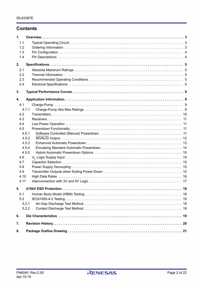
Figure 1. Typical Operating Circuit
Part Number(Notes 2, 3)
PartMarking Temp. Range (°C)
Tape and Reel(Units) (Note 1)
Package(RoHS Compliant) Pkg. Dwg. #.
ISL83387EIVZ 83387EIVZ -40 to 85 - 24 Ld TSSOP M24.173
ISL83387EIVZ-T 83387EIVZ -40 to 85 2.5k 24 Ld TSSOP M24.173
Notes:1. See TB347 for details about reel specifications.
2. Pb-free plus anneal products employ special Pb-free material sets; molding compounds/die attach materials and 100% matte tin plate termination finish, which are RoHS compliant and compatible with both SnPb and Pb-free soldering operations. Pb-free products are MSL classified at Pb-free peak reflow temperatures that meet or exceed the Pb-free requirements of IPC/JEDEC J-STD-020.
3. For Moisture Sensitivity Level (MSL), see the ISL83387E device page. For more information about MSL, see TB363.
23
VCC
T1OUT
T2OUT
T3OUT
T1IN
T2IN
T3IN
T1
T2
T3
0.1µF
+0.1µF
+0.1µF
7
8
21
20
10 19
1
3
2
6
V+
V-
C1+
C1-
C2+
C2-
+0.1µF
4
5
R1OUT R1IN18
5kΩ
R2OUT R2IN1713
5kΩ
R3OUT R3IN
1612
5kΩ
14
C1
C2
+ C3
C4
FORCEON
FORCEOFF
11
GND
24
+3.3V +0.1µF
22
VCC
TTL/CMOSLogic Levels
RS-232Levels
RS-232Levels
R1
R2
R3
9INVALID
To PowerControl Logic
VL15LOGIC VCC
+0.1µF
ISL83387E 1. Overview
FN6040 Rev.2.00 Page 4 of 22Apr.19.19
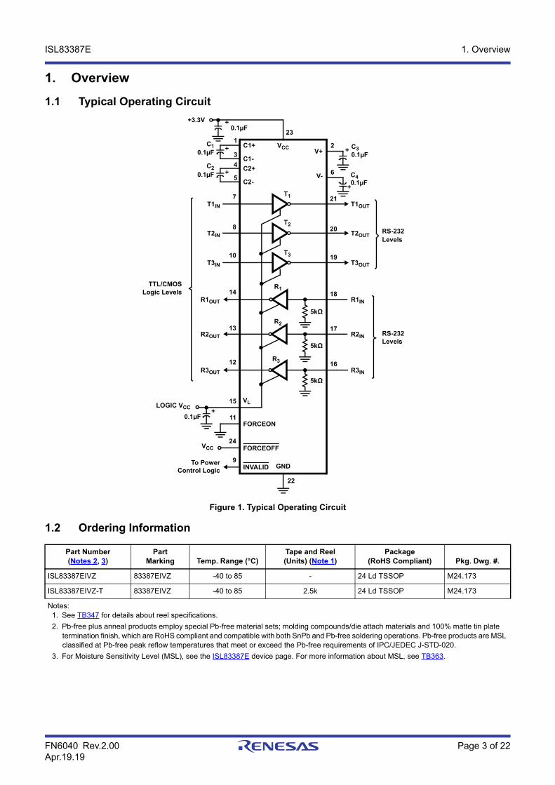
1.3 Pin Configuration
1.4 Pin Descriptions
TSSOPTop View
Pin Name Function
VCC System power supply input (3.0V to 5.5V).
V+ Internally generated positive transmitter supply (+5.5V).
V- Internally generated negative transmitter supply (-5.5V).
GND Ground connection.
C1+ External capacitor (voltage doubler) is connected to this lead.
C1- External capacitor (voltage doubler) is connected to this lead.
C2+ External capacitor (voltage inverter) is connected to this lead.
C2- External capacitor (voltage inverter) is connected to this lead.
TIN TTL/CMOS compatible transmitter Inputs. The switching point is a function of the VL voltage.
TOUT ±15kV ESD Protected, RS-232 level (nominally ±5.5V) transmitter outputs.
RIN ±15kV ESD Protected, RS-232 compatible receiver inputs.
ROUT TTL/CMOS level receiver outputs. Swings between GND and VL.
VL Logic-Level Supply. All TTL/CMOS inputs and outputs are powered by this supply.
INVALID Active low output that indicates if no valid RS-232 levels are present on any receiver input. Swings between GND and VL.
FORCEOFF Active low to shut down transmitters and on-chip power supply that overrides any automatic circuitry and FORCEON (see Table 5 on page 11). The switching point is a function of the VL voltage.
FORCEON Active high input to override automatic powerdown circuitry, which keeps transmitters active. (FORCEOFF must be high). The switching point is a function of the VL voltage.
C1+
V+
C1-
C2+
C2-
V-
T1IN
T2IN
INVALID
FORCEON
R3OUT
FORCEOFF
GND
T1OUT
T2OUT
T3OUT
R2IN
VL
R1OUT
R2OUT
VCC
R1IN
R3IN
24
23
22
21
20
19
18
17
16
15
14
13
1
2
3
4
5
6
7
8
9
10
11
12
T3IN
ISL83387E 2. Specifications
FN6040 Rev.2.00 Page 5 of 22Apr.19.19
2. Specifications
2.1 Absolute Maximum Ratings
2.2 Thermal Information
2.3 Recommended Operating Conditions
2.4 Electrical Specifications
Parameter Minimum Maximum Unit
VCC to Ground -0.3 6 V
VL to Ground -0.3 7 V
V+ to Ground -0.3 7 V
V- to Ground +0.3 -7 V
V+ to V- 14 V
Input Voltages
TIN,FORCEON, FORCEOFF -0.3 6 V
RIN ±25 V
Output Voltages
TOUT ±13.2 V
ROUT, INVALID -0.3 VL + 0.3 V
Short-Circuit Duration
TOUT Continuous
ESD Rating (See “ESD Performance” on page 7)
CAUTION: Do not operate at or near the maximum ratings listed for extended periods of time. Exposure to such conditions can adversely impact product reliability and result in failures not covered by warranty.
Thermal Resistance (Typical, Note 4) θJA (°C/W)
24 Ld TSSOP Package 140
Note: 4. θJA is measured with the component mounted on a low-effective thermal conductivity test board in free air. See TB379.
Parameter Minimum Maximum Unit
Maximum Junction Temperature (Plastic Package) +150 °C
Maximum Storage Temperature Range -65 +150 °C
Pb-Free Reflow Profile see TB493
Parameter Minimum Maximum Unit
Temperature Range -40 +85 °C
Test conditions: VCC = 3V to 5.5V, C1 - C4 = 0.1µF, VL = VCC; unless otherwise specified. Typicals are at TA = 25°C, VCC = VL = 3.3V
Parameter Test ConditionsTemp(°C) Min Typ Max Unit
DC Characteristics
Supply Current, Automatic Power-Down
All RIN Open, FORCEON = GND, FORCEOFF = VCC 25 - 1 10 µA
Supply Current, Powerdown FORCEOFF = GND 25 - 1 10 µA
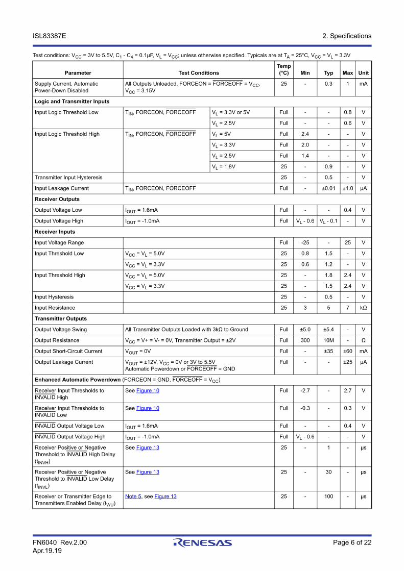
ISL83387E 2. Specifications
FN6040 Rev.2.00 Page 6 of 22Apr.19.19
Supply Current, Automatic Power-Down Disabled
All Outputs Unloaded, FORCEON = FORCEOFF = VCC, VCC = 3.15V
25 - 0.3 1 mA
Logic and Transmitter Inputs
Input Logic Threshold Low TIN, FORCEON, FORCEOFF VL = 3.3V or 5V Full - - 0.8 V
VL = 2.5V Full - - 0.6 V
Input Logic Threshold High TIN, FORCEON, FORCEOFF VL = 5V Full 2.4 - - V
VL = 3.3V Full 2.0 - - V
VL = 2.5V Full 1.4 - - V
VL = 1.8V 25 - 0.9 - V
Transmitter Input Hysteresis 25 - 0.5 - V
Input Leakage Current TIN, FORCEON, FORCEOFF Full - ±0.01 ±1.0 µA
Receiver Outputs
Output Voltage Low IOUT = 1.6mA Full - - 0.4 V
Output Voltage High IOUT = -1.0mA Full VL - 0.6 VL - 0.1 - V
Receiver Inputs
Input Voltage Range Full -25 - 25 V
Input Threshold Low VCC = VL = 5.0V 25 0.8 1.5 - V
VCC = VL = 3.3V 25 0.6 1.2 - V
Input Threshold High VCC = VL = 5.0V 25 - 1.8 2.4 V
VCC = VL = 3.3V 25 - 1.5 2.4 V
Input Hysteresis 25 - 0.5 - V
Input Resistance 25 3 5 7 kΩ
Transmitter Outputs
Output Voltage Swing All Transmitter Outputs Loaded with 3kΩ to Ground Full ±5.0 ±5.4 - V
Output Resistance VCC = V+ = V- = 0V, Transmitter Output = ±2V Full 300 10M - Ω
Output Short-Circuit Current VOUT = 0V Full - ±35 ±60 mA
Output Leakage Current VOUT = ±12V, VCC = 0V or 3V to 5.5VAutomatic Powerdown or FORCEOFF = GND
Full - - ±25 µA
Enhanced Automatic Powerdown (FORCEON = GND, FORCEOFF = VCC)
Receiver Input Thresholds to INVALID High
See Figure 10 Full -2.7 - 2.7 V
Receiver Input Thresholds to INVALID Low
See Figure 10 Full -0.3 - 0.3 V
INVALID Output Voltage Low IOUT = 1.6mA Full - - 0.4 V
INVALID Output Voltage High IOUT = -1.0mA Full VL - 0.6 - - V
Receiver Positive or Negative Threshold to INVALID High Delay (tINVH)
See Figure 13 25 - 1 - µs
Receiver Positive or Negative Threshold to INVALID Low Delay (tINVL)
See Figure 13 25 - 30 - µs
Receiver or Transmitter Edge to Transmitters Enabled Delay (tWU)
Note 5, see Figure 13 25 - 100 - µs
Test conditions: VCC = 3V to 5.5V, C1 - C4 = 0.1µF, VL = VCC; unless otherwise specified. Typicals are at TA = 25°C, VCC = VL = 3.3V
Parameter Test ConditionsTemp(°C) Min Typ Max Unit
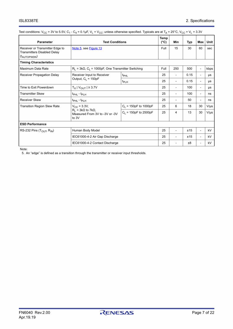
ISL83387E 2. Specifications
FN6040 Rev.2.00 Page 7 of 22Apr.19.19
Receiver or Transmitter Edge to Transmitters Disabled Delay (tAUTOPWDN)
Note 5, see Figure 13 Full 15 30 60 sec
Timing Characteristics
Maximum Data Rate RL = 3kΩ, CL = 1000pF, One Transmitter Switching Full 250 500 - kbps
Receiver Propagation Delay Receiver Input to Receiver Output, CL = 150pF
tPHL 25 - 0.15 - µs
tPLH 25 - 0.15 - µs
Time to Exit Powerdown TX | VOUT | ≥ 3.7V 25 - 100 - µs
Transmitter Skew tPHL - tPLH 25 - 100 - ns
Receiver Skew tPHL - tPLH 25 - 50 - ns
Transition Region Slew Rate VCC = 3.3V, RL = 3kΩ to 7kΩ,Measured From 3V to -3V or -3V to 3V
CL = 150pF to 1000pF 25 6 18 30 V/µs
CL = 150pF to 2500pF 25 4 13 30 V/µs
ESD Performance
RS-232 Pins (TOUT, RIN) Human Body Model 25 - ±15 - kV
IEC61000-4-2 Air Gap Discharge 25 - ±15 - kV
IEC61000-4-2 Contact Discharge 25 - ±8 - kV
Note: 5. An “edge” is defined as a transition through the transmitter or receiver input thresholds.
Test conditions: VCC = 3V to 5.5V, C1 - C4 = 0.1µF, VL = VCC; unless otherwise specified. Typicals are at TA = 25°C, VCC = VL = 3.3V
Parameter Test ConditionsTemp(°C) Min Typ Max Unit
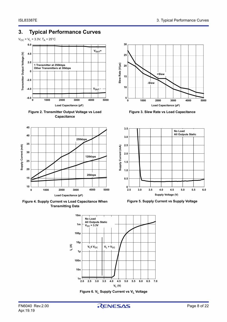
ISL83387E 3. Typical Performance Curves
FN6040 Rev.2.00 Page 8 of 22Apr.19.19
3. Typical Performance CurvesVCC = VL = 3.3V, TA = 25°C
Figure 2. Transmitter Output Voltage vs Load Capacitance
Figure 3. Slew Rate vs Load Capacitance
Figure 4. Supply Current vs Load Capacitance When Transmitting Data
Figure 5. Supply Current vs Supply Voltage
Figure 6. VL Supply Current vs VL Voltage
-6.0
-4.0
-2.0
0
2.0
4.0
6.0
1000 2000 3000 4000 50000
Load Capacitance (pF)
Tra
ns
mit
ter
Ou
tpu
t V
olt
ag
e (
V)
1 Transmitter at 250kbps
VOUT+
VOUT -
Other Transmitters at 30kbps
Load Capacitance (pF)
Sle
w R
ate
(V
/µs)
0 1000 2000 3000 4000 5000
-Slew
+Slew
5
10
15
20
25
30
10
15
20
25
30
45
35
40
0 1000 2000 3000 4000 5000
Load Capacitance (pF)
Su
pp
ly C
urr
ent
(mA
)
20kbps
250kbps
120kbps
Su
pp
ly C
urr
ent
(mA
)
2.5 3.0 3.5 4.0 4.5 5.0 5.5 6.00
0.5
1.0
1.5
2.0
Supply Voltage (V)
2.5
3.0
3.5No LoadAll Outputs Static
I L (
A)
VL (V)
No LoadAll Outputs Static
2.0 3.0 3.5 4.0 4.5 5.0 5.5 6.02.5 6.5 7.01n
10n
100n
1µ
10µ
100µ
10m
1m VCC = 3.3V
VL≤ VCC VL > VCC
ISL83387E 4. Application Information
FN6040 Rev.2.00 Page 9 of 22Apr.19.19
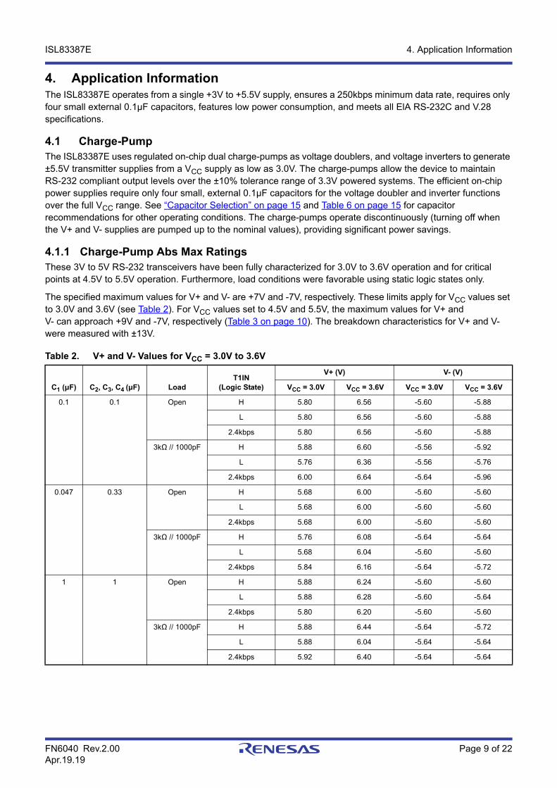
4. Application InformationThe ISL83387E operates from a single +3V to +5.5V supply, ensures a 250kbps minimum data rate, requires only four small external 0.1µF capacitors, features low power consumption, and meets all ElA RS-232C and V.28 specifications.
4.1 Charge-PumpThe ISL83387E uses regulated on-chip dual charge-pumps as voltage doublers, and voltage inverters to generate ±5.5V transmitter supplies from a VCC supply as low as 3.0V. The charge-pumps allow the device to maintain RS-232 compliant output levels over the ±10% tolerance range of 3.3V powered systems. The efficient on-chip power supplies require only four small, external 0.1µF capacitors for the voltage doubler and inverter functions over the full VCC range. See “Capacitor Selection” on page 15 and Table 6 on page 15 for capacitor recommendations for other operating conditions. The charge-pumps operate discontinuously (turning off when the V+ and V- supplies are pumped up to the nominal values), providing significant power savings.
4.1.1 Charge-Pump Abs Max RatingsThese 3V to 5V RS-232 transceivers have been fully characterized for 3.0V to 3.6V operation and for critical points at 4.5V to 5.5V operation. Furthermore, load conditions were favorable using static logic states only.
The specified maximum values for V+ and V- are +7V and -7V, respectively. These limits apply for VCC values set to 3.0V and 3.6V (see Table 2). For VCC values set to 4.5V and 5.5V, the maximum values for V+ and V- can approach +9V and -7V, respectively (Table 3 on page 10). The breakdown characteristics for V+ and V- were measured with ±13V.
Table 2. V+ and V- Values for VCC = 3.0V to 3.6V
C1 (μF) C2, C3, C4 (μF) LoadT1IN
(Logic State)
V+ (V) V- (V)
VCC = 3.0V VCC = 3.6V VCC = 3.0V VCC = 3.6V
0.1 0.1 Open H 5.80 6.56 -5.60 -5.88
L 5.80 6.56 -5.60 -5.88
2.4kbps 5.80 6.56 -5.60 -5.88
3kΩ // 1000pF H 5.88 6.60 -5.56 -5.92
L 5.76 6.36 -5.56 -5.76
2.4kbps 6.00 6.64 -5.64 -5.96
0.047 0.33 Open H 5.68 6.00 -5.60 -5.60
L 5.68 6.00 -5.60 -5.60
2.4kbps 5.68 6.00 -5.60 -5.60
3kΩ // 1000pF H 5.76 6.08 -5.64 -5.64
L 5.68 6.04 -5.60 -5.60
2.4kbps 5.84 6.16 -5.64 -5.72
1 1 Open H 5.88 6.24 -5.60 -5.60
L 5.88 6.28 -5.60 -5.64
2.4kbps 5.80 6.20 -5.60 -5.60
3kΩ // 1000pF H 5.88 6.44 -5.64 -5.72
L 5.88 6.04 -5.64 -5.64
2.4kbps 5.92 6.40 -5.64 -5.64
ISL83387E 4. Application Information
FN6040 Rev.2.00 Page 10 of 22Apr.19.19
The resulting new maximum voltages at V+ and V- are listed in Table 4.
4.2 TransmittersThe transmitters are proprietary, low dropout, inverting drivers that translate TTL/CMOS inputs to EIA/TIA-232 output levels. The transmitters couple with the on-chip ±5.5V supplies to deliver true RS-232 levels across a wide range of single supply system voltages.
All transmitter outputs disable and assume a high impedance state when the device enters the powerdown mode (see Table 5 on page 11). The outputs can be driven to ±12V when disabled.
The ISL83387E ensures a 250kbps data rate for full load conditions (3kΩ and 1000pF), VCC ≥ 3.0V, with one transmitter operating at full speed. Under more typical conditions of VCC ≥ 3.3V, RL = 3kΩ, and CL = 250pF, one transmitter easily operates at 1.25Mbps.
The transmitter input threshold is set by the voltage applied to the VL supply pin. Transmitter inputs float if they remain unconnected (there are no pull-up resistors), and they can cause ICC increases. Connect unused inputs to GND for best performance.
Table 3. V+ and V- Values for VCC = 4.5V to 5.5V
C1 (μF) C2, C3, C4 (μF) LoadT1IN
(Logic State)
V+ (V) V- (V)
VCC = 4.5V VCC = 5.5V VCC = 4.5V VCC = 5.5V
0.1 0.1 Open H 7.44 8.48 -6.16 -6.40
L 7.44 8.48 -6.16 -6.44
2.4kbps 7.44 8.48 -6.17 -6.44
3kΩ // 1000pF H 7.76 8.88 -6.36 -6.72
L 7.08 8.00 -5.76 -5.76
2.4kbps 7.76 8.84 -6.40 -6.64
0.047 0.33 Open H 6.44 6.88 -5.80 -5.88
L 6.48 6.88 -5.84 -5.88
2.4kbps 6.44 6.88 -5.80 -5.88
3kΩ // 1000pF H 6.64 7.28 -5.92 -6.04
L 6.24 6.60 -5.52 -5.52
2.4kbps 6.72 7.16 -5.92 -5.96
1 1 Open H 6.84 7.60 -5.76 -5.76
L 6.88 7.60 -5.76 -5.76
2.4kbps 6.92 7.56 -5.72 -5.76
3kΩ // 1000pF H 7.28 8.16 -5.80 -5.92
L 6.44 6.84 -5.64 -6.84
2.4kbps 7.08 7.76 -5.80 -5.80
Table 4. New Measured Withstanding Voltages
V+, V- to Ground ±13V
V+ to V- 20V
ISL83387E 4. Application Information
FN6040 Rev.2.00 Page 11 of 22Apr.19.19
4.3 ReceiversThe ISL83387E contains standard inverting receivers that convert RS-232 signals to CMOS output levels and accept inputs up to ±25V while presenting the required 3kΩ to 7kΩ input impedance (see Figure 7) even if the power is off (VCC = 0V). The receivers’ Schmitt trigger input stage uses hysteresis to increase noise immunity and decrease errors due to slow input signal transitions. Receiver outputs swing from GND to VL and do not tristate in powerdown (see Table 5).
4.4 Low Power OperationDuring normal operation (not in powerdown mode), this 3V device requires a nominal supply current of 0.3mA, even at VCC = 5.5V. This current is considerably less than the 11mA current required by comparable 5V RS-232 devices, and it allows you to reduce system power simply by replacing the old style device with the ISL83387E in new designs.
4.5 Powerdown FunctionalityThe already low current requirement drops significantly when the device enters powerdown mode. In power-down, the supply current drops to 1µA, because the on-chip charge-pump turns off (V+ collapses to VCC, V- collapses to GND) and the transmitter outputs tri-state. This micro-power mode makes the device ideal for battery powered and portable applications.
4.5.1 Software Controlled (Manual) PowerdownThe ISL83387E allows you to force the IC into the low power standby state and uses a two pin approach where the FORCEON and FORCEOFF inputs determine the IC’s mode. For always enabled operation, FORCEON and FORCEOFF are both strapped high. Under logic or software control, only the FORCEOFF input needs to be driven to switch between active and powerdown modes. The FORCEON state is not critical because FORCEOFF overrides FORCEON. However, if strictly manual control over powerdown is needed, you must strap FORCEON high to disable the automatic powerdown circuitry.
Figure 7. Receiver Connections
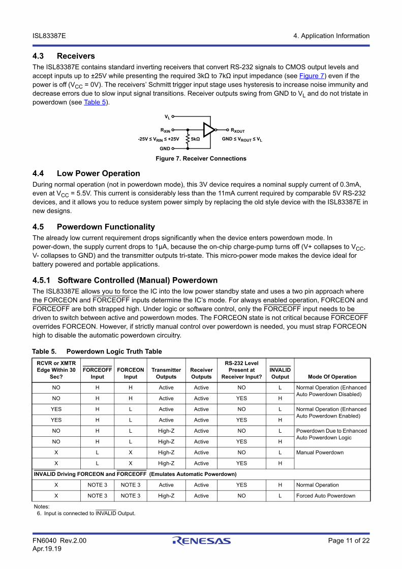
Table 5. Powerdown Logic Truth Table
RCVR or XMTR Edge Within 30
Sec?FORCEOFF
InputFORCEON
InputTransmitter
OutputsReceiverOutputs
RS-232 Level Present at
Receiver Input?INVALIDOutput Mode Of Operation
NO H H Active Active NO L Normal Operation (Enhanced Auto Powerdown Disabled)
NO H H Active Active YES H
YES H L Active Active NO L Normal Operation (Enhanced Auto Powerdown Enabled)
YES H L Active Active YES H
NO H L High-Z Active NO L Powerdown Due to Enhanced Auto Powerdown Logic
NO H L High-Z Active YES H
X L X High-Z Active NO L Manual Powerdown
X L X High-Z Active YES H
INVALID Driving FORCEON and FORCEOFF (Emulates Automatic Powerdown)
X NOTE 3 NOTE 3 Active Active YES H Normal Operation
X NOTE 3 NOTE 3 High-Z Active NO L Forced Auto Powerdown
Notes:6. Input is connected to INVALID Output.
RXOUT
GND ≤ VROUT ≤ VL5kΩ
RXIN
-25V ≤ VRIN ≤ +25V
GND
VL

ISL83387E 4. Application Information
FN6040 Rev.2.00 Page 12 of 22Apr.19.19
Connecting FORCEOFF and FORCEON together disables the enhanced automatic powerdown feature, enabling them to function as a manual SHUTDOWN input (see Figure 8).
With any of the control schemes, the time required to exit powerdown, and resume transmission is only 100µs.
When using both manual and enhanced automatic power-down (FORCEON = 0), the ISL83387E does not power up from manual powerdown until both FORCEOFF and FORCEON are driven high, or until a transition occurs on a receiver or transmitter input. Figure 9 shows a circuit for ensuring that the ISL83387E powers up as soon as FORCEOFF switches high. The rising edge of the master powerdown signal forces the device to power up, and the ISL83387E returns to enhanced automatic powerdown mode an RC time constant after this rising edge. The time constant isn’t critical, because the ISL83387E remains powered up for 30 seconds after the FORCEON falling edge, even if there are no signal transitions. The delay gives the slow-to-wake systems (such as a mouse) plenty of time to start transmitting, and as long as it starts transmitting within 30 seconds both systems remain enabled.
4.5.2 INVALID OutputThe INVALID output always indicates (see Table 5 on page 11) whether 30µs have elapsed with invalid RS-232 signals (see Figures 10 and 13) persisting on all of the receiver inputs, and it provides a way to determine when the interface block should power down. Invalid receiver levels occur whenever the driving peripheral’s outputs are shut off (powered down) or when the RS-232 interface cable is disconnected. If an interface cable is disconnected and all the receiver inputs are floating (but pulled to GND by the internal receiver pull down resistors), the INVALID logic detects the invalid levels and drives the output low. The power management logic then uses this indicator to power down the interface block. Reconnecting the cable restores valid levels at the receiver inputs,
Figure 8. Connections for Manual Powerdown
Figure 9. Circuit to Ensure Immediate Power Up When Exiting Forced Powerdown
Power
FORCEOFF, FORCEON
CPU I/O
ISL83387E
ManagementLogic
UART
VL
I/O ChipPower Supply
VCC
INVALID
FORCEOFF FORCEON
Power Master Powerdown Line
1MΩ0.1µFManagement
Unit
ISL83387E
ISL83387E 4. Application Information
FN6040 Rev.2.00 Page 13 of 22Apr.19.19
INVALID switches high, and the power management logic wakes up the interface block. INVALID can also be used to indicate the DTR or RING INDICATOR signal as long as the other receiver inputs are floating or driven to GND (as in the case of a powered down driver).
INVALID switches high 1µs after detecting a valid RS-232 level on a receiver input. INVALID operates in all modes (forced or automatic powerdown, or forced on), so it is also useful for systems employing manual power-down circuitry.
4.5.3 Enhanced Automatic PowerdownEven greater power savings are available by using the enhanced automatic powerdown function. When the enhanced powerdown logic determines that no transitions have occurred on any of the transmitter nor receiver inputs for 30 seconds, the charge-pump and transmitters power-down and reduce the supply current to 1µA. The ISL83387E automatically powers back up whenever it detects a transition on one of these inputs. This automatic powerdown feature provides additional system power savings without changes to the existing operating system.
Enhanced automatic powerdown operates when the FORCEON input is low, and the FORCEOFF input is high. Tying FORCEON high disables automatic powerdown, but manual powerdown is always available using the overriding FORCEOFF input. Table 5 summarizes the enhanced automatic powerdown functionality.
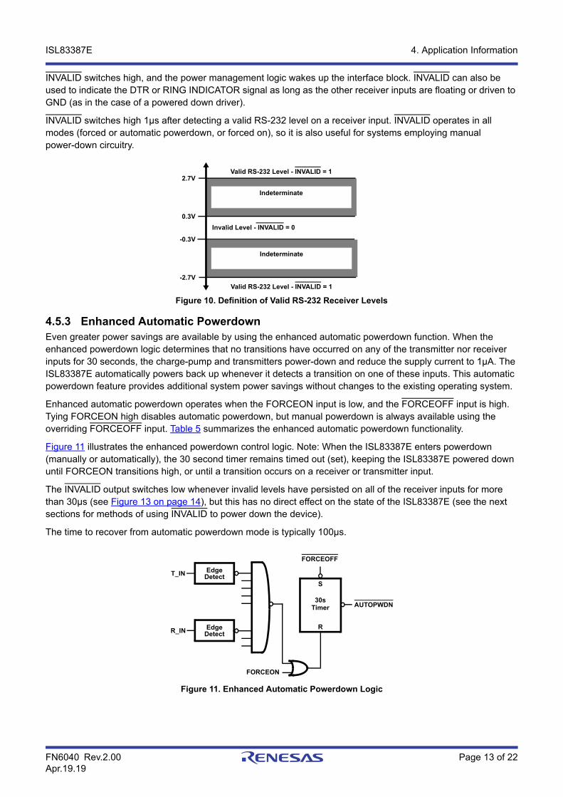
Figure 11 illustrates the enhanced powerdown control logic. Note: When the ISL83387E enters powerdown (manually or automatically), the 30 second timer remains timed out (set), keeping the ISL83387E powered down until FORCEON transitions high, or until a transition occurs on a receiver or transmitter input.
The INVALID output switches low whenever invalid levels have persisted on all of the receiver inputs for more than 30µs (see Figure 13 on page 14), but this has no direct effect on the state of the ISL83387E (see the next sections for methods of using INVALID to power down the device).
The time to recover from automatic powerdown mode is typically 100µs.
Figure 10. Definition of Valid RS-232 Receiver Levels
Figure 11. Enhanced Automatic Powerdown Logic
0.3V
-0.3V
-2.7V
2.7V
Invalid Level - INVALID = 0
Valid RS-232 Level - INVALID = 1
Valid RS-232 Level - INVALID = 1
Indeterminate
Indeterminate
30sTimer
S
R
FORCEOFF
AUTOPWDN
FORCEON
R_IN
T_IN EdgeDetect
EdgeDetect
ISL83387E 4. Application Information
FN6040 Rev.2.00 Page 14 of 22Apr.19.19
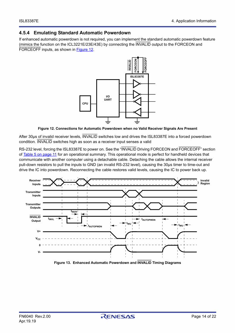
4.5.4 Emulating Standard Automatic PowerdownIf enhanced automatic powerdown is not required, you can implement the standard automatic powerdown feature (mimics the function on the ICL3221E/23E/43E) by connecting the INVALID output to the FORCEON and FORCEOFF inputs, as shown in Figure 12.
After 30µs of invalid receiver levels, INVALID switches low and drives the ISL83387E into a forced powerdown condition. INVALID switches high as soon as a receiver input senses a valid
RS-232 level, forcing the ISL83387E to power on. See the “INVALID Driving FORCEON and FORCEOFF” section of Table 5 on page 11 for an operational summary. This operational mode is perfect for handheld devices that communicate with another computer using a detachable cable. Detaching the cable allows the internal receiver pull-down resistors to pull the inputs to GND (an invalid RS-232 level), causing the 30µs timer to time-out and drive the IC into powerdown. Reconnecting the cable restores valid levels, causing the IC to power back up.
Figure 12. Connections for Automatic Powerdown when no Valid Receiver Signals Are Present
Figure 13. Enhanced Automatic Powerdown and INVALID Timing Diagrams
FO
RC
EO
FF
INV
AL
ID
CPU
I/O
FO
RC
EO
N
ISL83387E
UART
ReceiverInputs
TransmitterOutputs
INVALIDOutput
V+
VCC
0
V-
tINVL
tINVH
TransmitterInputs
tWU
tAUTOPWDN
tAUTOPWDNtWU
InvalidRegion
ISL83387E 4. Application Information
FN6040 Rev.2.00 Page 15 of 22Apr.19.19
4.5.5 Hybrid Automatic Powerdown OptionsFor devices that communicate only through a detachable cable, INVALID can be connected to FORCEOFF (with FORCEON = 0). While the cable is attached, INVALID and FORCEOFF remain high, so the enhanced automatic powerdown logic powers down the ISL83387E whenever there is 30 seconds of inactivity on the receiver and transmitter inputs. Detaching the cable allows the receiver inputs to drop to an invalid level (GND), so INVALID switches low and forces the ISL83387E to power down. The ISL83387E remains powered down until the cable is reconnected (INVALID = FORCEOFF = 1), and a transition occurs on a receiver or transmitter input (see Figure 11). For immediate power up when the cable is reattached, connect FORCEON to FORCEOFF through a network similar to that shown in Figure 9 on page 12.
4.6 VL Logic Supply InputUnlike other RS-232 interface devices where the CMOS outputs swing between 0 and VCC, the ISL83387E features a separate logic supply input (VL; 1.8V to 5V, regardless of VCC) that sets VOH for the receiver and INVALID outputs. Connecting VL to a host logic supply lower than VCC, prevents the ISL83387E outputs from forward biasing the input diodes of a logic device powered by that lower supply. Connecting VL to a logic supply greater than VCC ensures that the receiver and INVALID output levels are compatible even with the CMOS input VIH of AC, HC, and CD4000 devices. Note: The VL supply current increases to 100µA with VL = 5V and VCC = 3.3V (see Figure 6). VL also powers the transmitter and logic inputs, thereby setting their switching thresholds to levels compatible with the logic supply. This separate logic supply pin allows a great deal of flexibility in interfacing to systems with different logic supplies. If logic translation is not required, connect VL to the ISL83387E VCC.
4.7 Capacitor SelectionThe ISL83387E charge-pumps require only 0.1µF capacitors for the full operational voltage range. Table 6 lists other acceptable capacitor values for various supply voltage ranges. Do not use values smaller than those listed in Table 6. Increasing the capacitor values (by a factor of 2) reduces ripple on the transmitter outputs and slightly reduces power consumption.
When using minimum required capacitor values, make sure that capacitor values do not degrade excessively with temperature. If in doubt, use capacitors with a larger nominal value. The capacitor’s Equivalent Series Resistance (ESR) usually rises at low temperatures, and it influences the amount of ripple on V+ and V-.
4.8 Power Supply DecouplingIn most circumstances a 0.1µF bypass capacitor is adequate. In applications that are particularly sensitive to power supply noise, decouple VCC to ground with a capacitor of the same value as the charge-pump capacitor C1. Connect the bypass capacitor as close as possible to the IC.
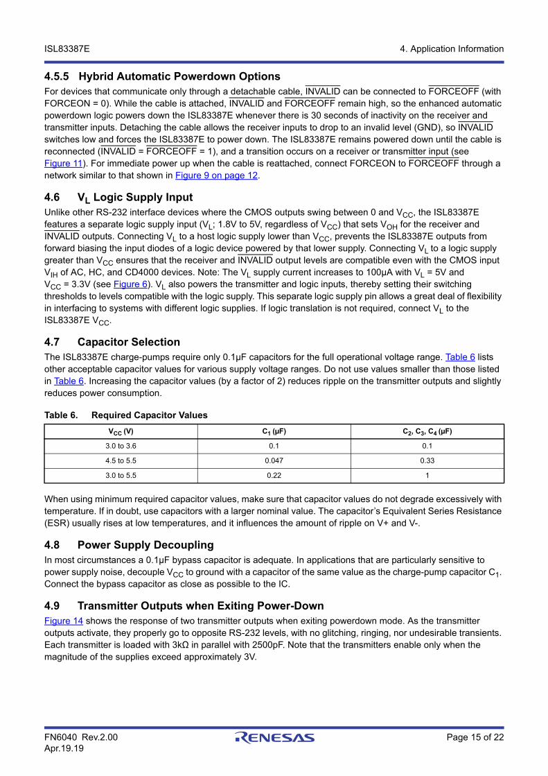
4.9 Transmitter Outputs when Exiting Power-DownFigure 14 shows the response of two transmitter outputs when exiting powerdown mode. As the transmitter outputs activate, they properly go to opposite RS-232 levels, with no glitching, ringing, nor undesirable transients. Each transmitter is loaded with 3kΩ in parallel with 2500pF. Note that the transmitters enable only when the magnitude of the supplies exceed approximately 3V.
Table 6. Required Capacitor Values
VCC (V) C1 (µF) C2, C3, C4 (µF)
3.0 to 3.6 0.1 0.1
4.5 to 5.5 0.047 0.33
3.0 to 5.5 0.22 1
ISL83387E 4. Application Information
FN6040 Rev.2.00 Page 16 of 22Apr.19.19
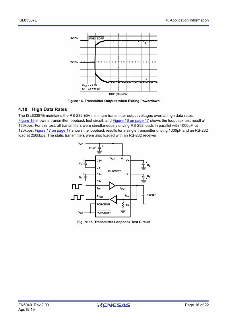
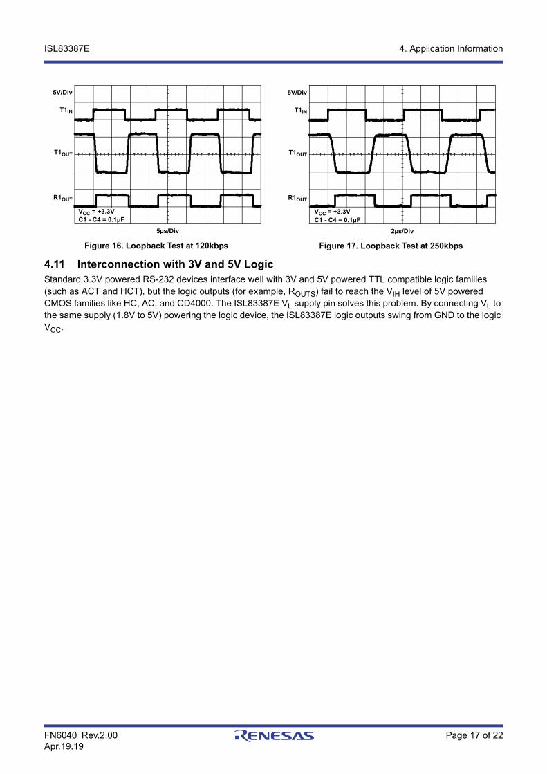
4.10 High Data RatesThe ISL83387E maintains the RS-232 ±5V minimum transmitter output voltages even at high data rates. Figure 15 shows a transmitter loopback test circuit, and Figure 16 on page 17 shows the loopback test result at 120kbps. For this test, all transmitters were simultaneously driving RS-232 loads in parallel with 1000pF, at 120kbps. Figure 17 on page 17 shows the loopback results for a single transmitter driving 1000pF and an RS-232 load at 250kbps. The static transmitters were also loaded with an RS-232 receiver.
Figure 14. Transmitter Outputs when Exiting Powerdown
Figure 15. Transmitter Loopback Test Circuit
TIME (20µs/Div)
T1
2V/Div
5V/Div
VCC = +3.3VC1 - C4 = 0.1µF
T2
FORCEOFF
ISL83387E
VCC
C1
C2C4
C3
+
++
+
1000pF
V+
V-
5k
TIN
ROUT
C1+
C1-
C2+
C2-
RIN
TOUT
+VCC
0.1µF
VCC
FORCEOFF
FORCEON
VL
ISL83387E 4. Application Information
FN6040 Rev.2.00 Page 17 of 22Apr.19.19
4.11 Interconnection with 3V and 5V LogicStandard 3.3V powered RS-232 devices interface well with 3V and 5V powered TTL compatible logic families (such as ACT and HCT), but the logic outputs (for example, ROUTS) fail to reach the VIH level of 5V powered CMOS families like HC, AC, and CD4000. The ISL83387E VL supply pin solves this problem. By connecting VL to the same supply (1.8V to 5V) powering the logic device, the ISL83387E logic outputs swing from GND to the logic VCC.
Figure 16. Loopback Test at 120kbps Figure 17. Loopback Test at 250kbps
T1IN
T1OUT
R1OUT
5µs/Div
VCC = +3.3V
5V/Div
C1 - C4 = 0.1µF
T1IN
T1OUT
R1OUT
2µs/Div
5V/Div
VCC = +3.3VC1 - C4 = 0.1µF
ISL83387E 5. ±15kV ESD Protection
FN6040 Rev.2.00 Page 18 of 22Apr.19.19
5. ±15kV ESD ProtectionAll pins on the 3V interface devices include ESD protection structures, but the ISL83387E incorporates advanced structures that allow the RS-232 pins (transmitter outputs and receiver inputs) to survive ESD events up to ±15kV. The RS-232 pins are particularly vulnerable to ESD damage because they typically connect to an exposed port on the exterior of the finished product. Touching the port pins, or connecting a cable, can cause an ESD event that might destroy unprotected ICs. The ESD structures protect the device whether or not it is powered up, protect without allowing any latch-up mechanism to activate, and do not interfere with RS-232 signals as large as ±25V.
5.1 Human Body Model (HBM) TestingThe Human Body Model (HBM) test method emulates the ESD event delivered to an IC during human handling. The tester delivers the charge through a 1.5kΩ current limiting resistor, so the test is less severe than the IEC61000 test, which uses a 330Ω limiting resistor. The HBM method determines an IC’s ability to withstand the ESD transients typically present during handling and manufacturing. Due to the random nature of these events, each pin is tested with respect to all other pins. The RS-232 pins on “E” family devices can withstand HBM ESD events to ±15kV.
5.2 IEC61000-4-2 TestingThe IEC61000 test method applies to finished equipment rather than to an individual IC. Therefore, the pins most likely to suffer an ESD event are those that are exposed to the outside world (the RS-232 pins in this case), and the IC is tested in its typical application configuration (power applied) rather than testing each pin-to-pin combination. The lower current limiting resistor coupled with the larger charge storage capacitor yields a test that is much more severe than the HBM test. The extra ESD protection built into this device’s RS-232 pins allows the design of equipment that meets Level 4 criteria without the need for additional board level protection on the RS-232 port.
5.2.1 Air-Gap Discharge Test MethodFor the air-gap discharge test method, a charged probe tip moves toward the IC pin until the voltage arcs to it. The current waveform delivered to the IC pin depends on factors such as approach speed, humidity, and temperature, so it is difficult to obtain repeatable results. The “E” device RS-232 pins withstand ±15kV air-gap discharges.
5.2.2 Contact Discharge Test MethodDuring the contact discharge test, the probe contacts the tested pin before the probe tip is energized and eliminates the variables associated with the air-gap discharge. The result is a more repeatable and predictable test, but equipment limits prevent testing devices at voltages higher than ±8kV. All “E” family devices survive ±8kV contact discharges on the RS-232 pins.
ISL83387E 6. Die Characteristics
FN6040 Rev.2.00 Page 19 of 22Apr.19.19
6. Die Characteristics
Substrate Potential (Powered Up) GND
Transistor Count 1063
Process Si Gate CMOS
ISL83387E 7. Revision History
FN6040 Rev.2.00 Page 20 of 22Apr.19.19
7. Revision History
Rev. Date Description
2.00 Apr.19.19 Applied new format.Updated Links throughout document.Updated Ordering Information table by removing retired parts and updating notes.Added “Charge-Pump Abs Max Ratings” on page 9.Added Revision HistoryUpdated package outline drawing M28.173 from revision 0 to revision 1.
Convert to new POD format by moving dimensions from table onto drawing and adding land pattern. Nodimension changes.
Updated Disclaimer.
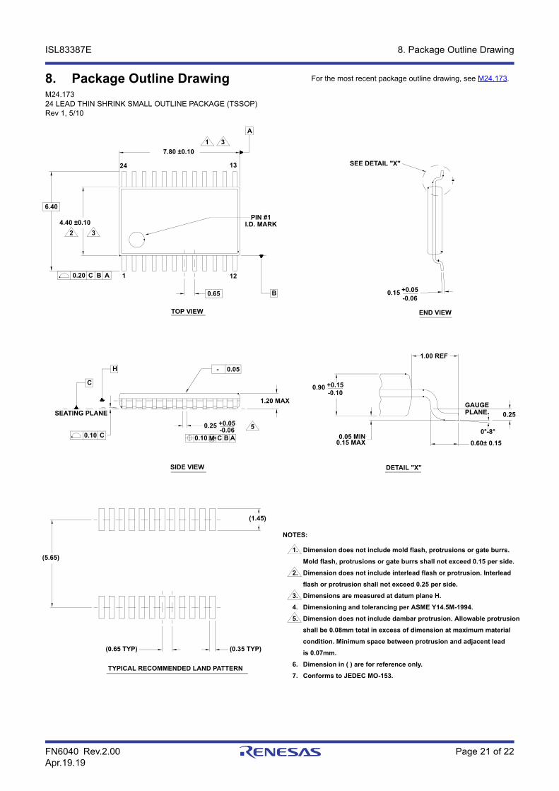
ISL83387E 8. Package Outline Drawing
FN6040 Rev.2.00 Page 21 of 22Apr.19.19
8. Package Outline DrawingM24.17324 LEAD THIN SHRINK SMALL OUTLINE PACKAGE (TSSOP)Rev 1, 5/10
DETAIL "X"
TYPICAL RECOMMENDED LAND PATTERN
TOP VIEW
SIDE VIEW
END VIEW
Dimension does not include mold flash, protrusions or gate burrs.
Mold flash, protrusions or gate burrs shall not exceed 0.15 per side.
Dimension does not include interlead flash or protrusion. Interlead
flash or protrusion shall not exceed 0.25 per side.
Dimensions are measured at datum plane H.
Dimensioning and tolerancing per ASME Y14.5M-1994.
Dimension does not include dambar protrusion. Allowable protrusion
shall be 0.08mm total in excess of dimension at maximum material
condition. Minimum space between protrusion and adjacent lead
is 0.07mm.
Dimension in ( ) are for reference only.
Conforms to JEDEC MO-153.
6.
3.
5.
4.
2.
1.
NOTES:
7.
5
SEATING PLANE
C
H
32
1
24
B
12
1 3
13
A
PLANEGAUGE
0.05 MIN0.15 MAX
0°-8°
0.60± 0.15
0.90
1.00 REF
0.25
SEE DETAIL "X"
0.15
0.25
(0.65 TYP)
(5.65)
(0.35 TYP)
(1.45)
6.40
4.40 ±0.10
0.65
1.20 MAX
PIN #1I.D. MARK
7.80 ±0.10
+0.05-0.06
-0.06+0.05
-0.10+0.15
0.20 C B A
0.10 C
- 0.05
0.10 C B AM
For the most recent package outline drawing, see M24.173.
Corporate HeadquartersTOYOSU FORESIA, 3-2-24 Toyosu,Koto-ku, Tokyo 135-0061, Japanwww.renesas.com
Contact InformationFor further information on a product, technology, the most up-to-date version of a document, or your nearest sales office, please visit:
www.renesas.com/contact/
TrademarksRenesas and the Renesas logo are trademarks of Renesas Electronics Corporation. All trademarks and registered trademarks are the property of their respective owners.
![EE-EP t u { z v z u B sEE-EP t u { z v z u B s RISTVIITED SEOTUD TAOTLUSTELE [0001] See taotlus on osaliselt jätk rahvusvahelisele patenditaotlusele nr PCT/USβ009/0γ4448, mis esitati](https://static.fdocument.org/doc/165x107/603c4579c0c5060f991662d9/ee-ep-t-u-z-v-z-u-b-s-ee-ep-t-u-z-v-z-u-b-s-ristviited-seotud-taotlustele-0001.jpg)
![Index [assets.cambridge.org]assets.cambridge.org/.../index/9781107011687_index.pdf · Index Aβ see amyloid-β ABILHAND questionnaire 591 abundance, in motor system 602–5 acarbose](https://static.fdocument.org/doc/165x107/5f031f417e708231d407a572/index-index-a-see-amyloid-abilhand-questionnaire-591-abundance-in-motor.jpg)