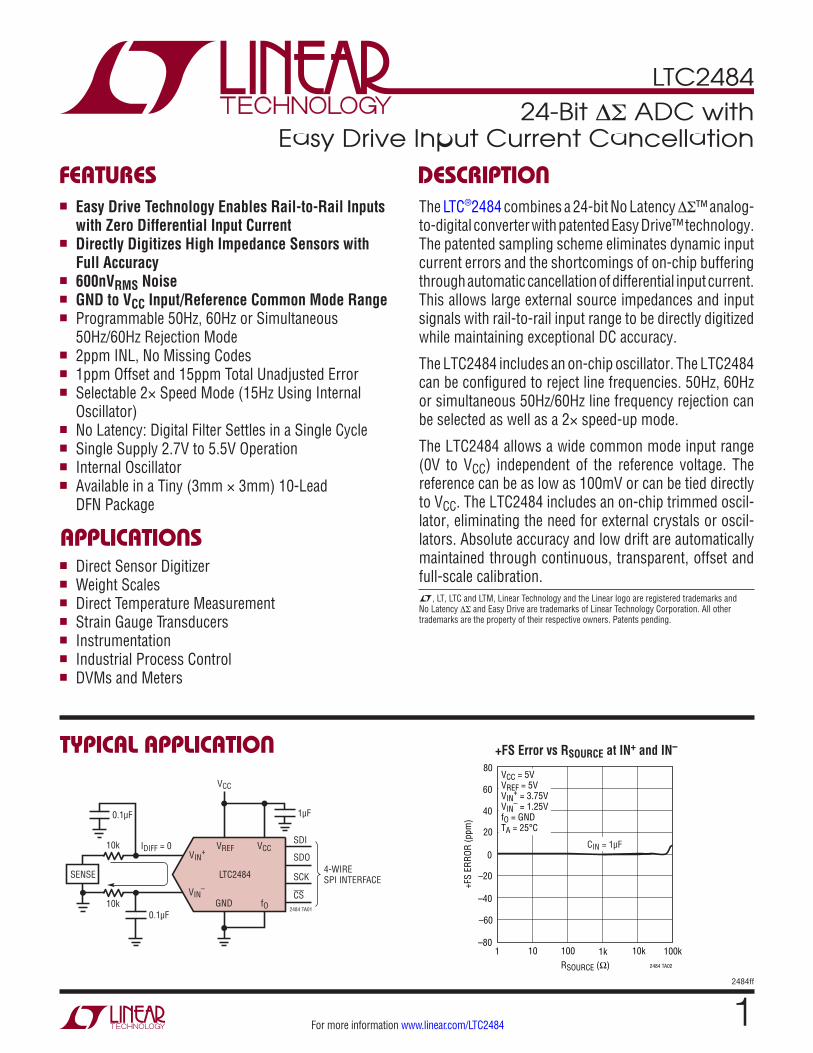
LTC2484 - 24-Bit ∆∑ ADC with Easy Drive Input Current ... 2 1 fO SCK GND SDO CS SDI VCC VREF IN+...
42
LTC2484 1 2484ff For more information www.linear.com/LTC2484 TYPICAL APPLICATION FEATURES APPLICATIONS DESCRIPTION 24-Bit ∆Σ ADC with Easy Drive Input Current Cancellation The LTC ® 2484 combines a 24-bit No Latency ∆Σ™ analog- to-digital converter with patented Easy Drive™ technology. The patented sampling scheme eliminates dynamic input current errors and the shortcomings of on-chip buffering through automatic cancellation of differential input current. This allows large external source impedances and input signals with rail-to-rail input range to be directly digitized while maintaining exceptional DC accuracy. The LTC2484 includes an on-chip oscillator. The LTC2484 can be configured to reject line frequencies. 50Hz, 60Hz or simultaneous 50Hz/60Hz line frequency rejection can be selected as well as a 2× speed-up mode. The LTC2484 allows a wide common mode input range (0V to V CC ) independent of the reference voltage. The reference can be as low as 100mV or can be tied directly to V CC . The LTC2484 includes an on-chip trimmed oscil- lator, eliminating the need for external crystals or oscil- lators. Absolute accuracy and low drift are automatically maintained through continuous, transparent, offset and full-scale calibration. n Easy Drive Technology Enables Rail-to-Rail Inputs with Zero Differential Input Current n Directly Digitizes High Impedance Sensors with Full Accuracy n 600nV RMS Noise n GND to V CC Input/Reference Common Mode Range n Programmable 50Hz, 60Hz or Simultaneous 50Hz/60Hz Rejection Mode n 2ppm INL, No Missing Codes n 1ppm Offset and 15ppm Total Unadjusted Error n Selectable 2× Speed Mode (15Hz Using Internal Oscillator) n No Latency: Digital Filter Settles in a Single Cycle n Single Supply 2.7V to 5.5V Operation n Internal Oscillator n Available in a Tiny (3mm × 3mm) 10-Lead DFN Package n Direct Sensor Digitizer n Weight Scales n Direct Temperature Measurement n Strain Gauge Transducers n Instrumentation n Industrial Process Control n DVMs and Meters L, LT, LTC and LTM, Linear Technology and the Linear logo are registered trademarks and No Latency ∆Σ and Easy Drive are trademarks of Linear Technology Corporation. All other trademarks are the property of their respective owners. Patents pending. LTC2484 V REF V CC V CC GND f O 1μF SDO 4-WIRE SPI INTERFACE 0.1μF 10k I DIFF = 0 10k 0.1μF SCK 2484 TA01 CS SDI SENSE V IN + V IN – R SOURCE (Ω) 1 +FS ERROR (ppm) –20 0 20 1k 100k 2484 TA02 –40 –60 –80 10 100 10k 40 60 80 V CC = 5V V REF = 5V V IN + = 3.75V V IN – = 1.25V f O = GND T A = 25°C C IN = 1μF +FS Error vs R SOURCE at IN + and IN –
-
Upload
hoangkhanh -
Category
Documents
-
view
225 -
download
2
Transcript of LTC2484 - 24-Bit ∆∑ ADC with Easy Drive Input Current ... 2 1 fO SCK GND SDO CS SDI VCC VREF IN+...
LTC2484
12484ff
For more information www.linear.com/LTC2484
Typical applicaTion
FeaTures
applicaTions
DescripTion
24-Bit ∆Σ ADC with Easy Drive Input Current Cancellation
The LTC®2484 combines a 24-bit No Latency ∆Σ™ analog-to-digital converter with patented Easy Drive™ technology. The patented sampling scheme eliminates dynamic input current errors and the shortcomings of on-chip buffering through automatic cancellation of differential input current. This allows large external source impedances and input signals with rail-to-rail input range to be directly digitized while maintaining exceptional DC accuracy.
The LTC2484 includes an on-chip oscillator. The LTC2484 can be configured to reject line frequencies. 50Hz, 60Hz or simultaneous 50Hz/60Hz line frequency rejection can be selected as well as a 2× speed-up mode.
The LTC2484 allows a wide common mode input range (0V to VCC) independent of the reference voltage. The reference can be as low as 100mV or can be tied directly to VCC. The LTC2484 includes an on-chip trimmed oscil-lator, eliminating the need for external crystals or oscil-lators. Absolute accuracy and low drift are automatically maintained through continuous, transparent, offset and full-scale calibration.
n Easy Drive Technology Enables Rail-to-Rail Inputs with Zero Differential Input Current
n Directly Digitizes High Impedance Sensors with Full Accuracy
n 600nVRMS Noisen GND to VCC Input/Reference Common Mode Rangen Programmable 50Hz, 60Hz or Simultaneous 50Hz/60Hz Rejection Moden 2ppm INL, No Missing Codesn 1ppm Offset and 15ppm Total Unadjusted Errorn Selectable 2× Speed Mode (15Hz Using Internal
Oscillator)n No Latency: Digital Filter Settles in a Single Cyclen Single Supply 2.7V to 5.5V Operationn Internal Oscillatorn Available in a Tiny (3mm × 3mm) 10-Lead DFN Package
n Direct Sensor Digitizern Weight Scalesn Direct Temperature Measurementn Strain Gauge Transducersn Instrumentationn Industrial Process Controln DVMs and Meters
L, LT, LTC and LTM, Linear Technology and the Linear logo are registered trademarks and No Latency ∆Σ and Easy Drive are trademarks of Linear Technology Corporation. All other trademarks are the property of their respective owners. Patents pending.
LTC2484
VREF VCC
VCC
GND fO
1µF
SDO4-WIRESPI INTERFACE
0.1µF
10k IDIFF = 0
10k0.1µF
SCK
2484 TA01
CS
SDI
SENSE
VIN+
VIN–
RSOURCE (Ω)1
+FS
ERRO
R (p
pm)
–20
0
20
1k 100k2484 TA02
–40
–60
–8010 100 10k
40
60
80VCC = 5VVREF = 5VVIN
+ = 3.75VVIN
– = 1.25VfO = GNDTA = 25°C
CIN = 1µF
+FS Error vs RSOURCE at IN+ and IN–
LTC2484
22484ff
For more information www.linear.com/LTC2484
absoluTe MaxiMuM raTings
Supply Voltage (VCC) to GND ...................... –0.3V to 6VAnalog Input Voltage to GND ....... –0.3V to (VCC + 0.3V)Reference Input Voltage to GND .. –0.3V to (VCC + 0.3V)Digital Input Voltage to GND ........ –0.3V to (VCC + 0.3V)Digital Output Voltage to GND ...... –0.3V to (VCC + 0.3V)Operating Temperature Range LTC2484C ............................................... 0°C to 70°C LTC2484I ...........................................–40°C to 85°C Storage Temperature Range ................. –65°C to 125°C
(Note 1)
elecTrical characTerisTics (norMal speeD) The l denotes the specifications which apply over the full operating temperature range, otherwise specifications are at TA = 25°C. (Notes 3, 4)
PARAMETER CONDITIONS MIN TYP MAX UNITS
Resolution (No Missing Codes) 0.1 ≤ VREF ≤ VCC, –FS ≤ VIN ≤ +FS (Note 5) l 24 Bits
Integral Nonlinearity 5V ≤ VCC ≤ 5.5V, VREF = 5V, VIN(CM) = 2.5V (Note 6) 2.7V ≤ VCC ≤ 5.5V, VREF = 2.5V, VIN(CM) = 1.25V (Note 6)
l 2 1
10 ppm of VREF ppm of VREF
Offset Error 2.5V ≤ VREF ≤ VCC, GND ≤ IN+ = IN– ≤ VCC (Note 14) l 0.5 2.5 µV
Offset Error Drift 2.5V ≤ VREF ≤ VCC, GND ≤ IN+ = IN– ≤ VCC 10 nV/°C
Positive Full-Scale Error 2.5V ≤ VREF ≤ VCC, IN+ = 0.75VREF , IN– = 0.25VREF l 25 ppm of VREF
Positive Full-Scale Error Drift 2.5V ≤ VREF ≤ VCC, IN+ = 0.75VREF , IN– = 0.25VREF 0.1 ppm of VREF/°C
Negative Full-Scale Error 2.5V ≤ VREF ≤ VCC, IN+ = 0.75VREF , IN– = 0.25VREF l 25 ppm of VREF
Negative Full-Scale Error Drift 2.5V ≤ VREF ≤ VCC, IN+ = 0.75VREF , IN– = 0.25VREF 0.1 ppm of VREF/°C
Total Unadjusted Error 5V ≤ VCC ≤ 5.5V, VREF = 2.5V, VIN(CM) = 1.25V 5V ≤ VCC ≤ 5.5V, VREF = 5V, VIN(CM) = 2.5V 2.7V ≤ VCC ≤ 5.5V, VREF = 2.5V, VIN(CM) = 1.25V
15 ppm of VREF ppm of VREF ppm of VREF
Output Noise 5V ≤ VCC ≤ 5.5V, VREF = 5V, GND ≤ IN– = IN+ ≤ VCC (Note 13) 0.6 µVRMS
Internal PTAT Signal TA = 27°C 390 450 mV
pin conFiguraTionTOP VIEW
11GND
DD PACKAGE10-LEAD (3mm × 3mm) PLASTIC DFN
10
9
6
7
8
4
5
3
2
1 fOSCK
GND
SDO
CS
SDI
VCC
VREF
IN+
IN–
TJMAX = 125°C, θJA = 43°C/W
EXPOSED PAD (PIN 11) IS GND, MUST BE SOLDERED TO PCB
orDer inForMaTionLEAD FREE FINISH TAPE AND REEL PART MARKING* PACKAGE DESCRIPTION TEMPERATURE RANGE
LTC2484CDD#PBF LTC2484CDD#TRPBF LBSS 10-Lead (3mm × 3mm) Plastic DFN 0°C to 70°C
LTC2484IDD#PBF LTC2484IDD#TRPBF LBSS 10-Lead (3mm × 3mm) Plastic DFN –40°C to 85°C
Consult LTC Marketing for parts specified with wider operating temperature ranges. *The temperature grade is identified by a label on the shipping container.For more information on lead free part marking, go to: http://www.linear.com/leadfree/ For more information on tape and reel specifications, go to: http://www.linear.com/tapeandreel/
LTC2484
32484ff
For more information www.linear.com/LTC2484
PARAMETER CONDITIONS MIN TYP MAX UNITS
Resolution (No Missing Codes) 0.1 ≤ VREF ≤ VCC, –FS ≤ VIN ≤ +FS (Note 5) l 24 Bits
Integral Nonlinearity 5V ≤ VCC ≤ 5.5V, VREF = 5V, VIN(CM) = 2.5V (Note 6) 2.7V ≤ VCC ≤ 5.5V, VREF = 2.5V, VIN(CM) = 1.25V (Note 6)
l 2 1
10 ppm of VREF ppm of VREF
Offset Error 2.5V ≤ VREF ≤ VCC, GND ≤ IN+ = IN– ≤ VCC (Note 14) l 0.5 2 mV
Offset Error Drift 2.5V ≤ VREF ≤ VCC, GND ≤ IN+ = IN– ≤ VCC 100 nV/°C
Positive Full-Scale Error 2.5V ≤ VREF ≤ VCC, IN+ = 0.75VREF, IN– = 0.25VREF l 25 ppm of VREF
Positive Full-Scale Error Drift 2.5V ≤ VREF ≤ VCC, IN+ = 0.75VREF, IN– = 0.25VREF 0.1 ppm of VREF/°C
Negative Full-Scale Error 2.5V ≤ VREF ≤ VCC, IN+ = 0.75VREF, IN– = 0.25VREF l 25 ppm of VREF
Negative Full-Scale Error Drift 2.5V ≤ VREF ≤ VCC, IN+ = 0.75VREF, IN– = 0.25VREF 0.1 ppm of VREF/°C
Output Noise 5V ≤ VCC ≤ 5.5V, VREF = 5V, GND ≤ IN– = IN+ ≤ VCC (Note 13) 0.84 µVRMS
converTer characTerisTics The l denotes the specifications which apply over the full operating temperature range, otherwise specifications are at TA = 25°C. (Notes 3, 4)
PARAMETER CONDITIONS MIN TYP MAX UNITS
Input Common Mode Rejection DC 2.5V ≤ VREF ≤ VCC, GND ≤ IN– = IN+ ≤ VCC (Note 5) l 140 dB
Input Common Mode Rejection 50Hz ±2%
2.5V ≤ VREF ≤ VCC, GND ≤ IN– = IN+ ≤ VCC (Note 5) l 140 dB
Input Common Mode Rejection 60Hz ±2%
2.5V ≤ VREF ≤ VCC, GND ≤ IN– = IN+ ≤ VCC (Note 5) l 140 dB
Input Normal Mode Rejection 50Hz ±2%
2.5V ≤ VREF ≤ VCC, GND ≤ IN– = IN+ ≤ VCC (Notes 5, 7) l 110 120 dB
Input Normal Mode Rejection 60Hz ±2%
2.5V ≤ VREF ≤ VCC, GND ≤ IN– = IN+ ≤ VCC (Notes 5, 8) l 110 120 dB
Input Normal Mode Rejection 50Hz/60Hz ±2%
2.5V ≤ VREF ≤ VCC, GND ≤ IN– = IN+ ≤ VCC (Notes 5, 9) l 87 dB
Reference Common Mode Rejection DC
2.5V ≤ VREF ≤ VCC, GND ≤ IN– = IN+ ≤ VCC (Note 5) l 120 140 dB
Power Supply Rejection DC VREF = 2.5V, IN– = IN+ = GND 120 dB
Power Supply Rejection, 50Hz ±2% VREF = 2.5V, IN– = IN+ = GND (Note 7) 120 dB
Power Supply Rejection, 60Hz ±2% VREF = 2.5V, IN– = IN+ = GND (Note 8) 120 dB
analog inpuT anD reFerence The l denotes the specifications which apply over the full operating temperature range, otherwise specifications are at TA = 25°C. (Note 3)
SYMBOL PARAMETER CONDITIONS MIN TYP MAX UNITS
IN+ Absolute/Common Mode IN+ Voltage GND – 0.3V VCC + 0.3V V
IN– Absolute/Common Mode IN– Voltage GND – 0.3V VCC + 0.3V V
FS Full-Scale of the Differential Input (IN+ – IN–) l 0.5VREF V
LSB Least Significant Bit of the Output Code l FS/224
VIN Input Differential Voltage Range (IN+ – IN–) l –FS +FS V
VREF Reference Voltage Range l 0.1 VCC V
elecTrical characTerisTics (2x speeD) The l denotes the specifications which apply over the full operating temperature range, otherwise specifications are at TA = 25°C. (Notes 3, 4)
LTC2484
42484ff
For more information www.linear.com/LTC2484
analog inpuT anD reFerence The l denotes the specifications which apply over the full operating temperature range, otherwise specifications are at TA = 25°C. (Note 3)
SYMBOL PARAMETER CONDITIONS MIN TYP MAX UNITS
CS (IN+) IN+ Sampling Capacitance 11 pF
CS (IN–) IN– Sampling Capacitance 11 pF
CS (VREF) VREF Sampling Capacitance 11 pF
IDC_LEAK (IN+) IN+ DC Leakage Current Sleep Mode, IN+ = GND l –10 1 10 nA
IDC_LEAK (IN–) IN– DC Leakage Current Sleep Mode, IN– = GND l –10 1 10 nA
IDC_LEAK (VREF) VREF DC Leakage Current Sleep Mode, VREF = VCC l –100 1 100 nA
DigiTal inpuTs anD DigiTal ouTpuTs The l denotes the specifications which apply over the full operating temperature range, otherwise specifications are at TA = 25°C. (Note 3)
SYMBOL PARAMETER CONDITIONS MIN TYP MAX UNITS
VIH High Level Input Voltage CS, fO, SDI
2.7V ≤ VCC ≤ 5.5V (Note 16) l VCC – 0.5 V
VIL Low Level Input Voltage CS, fO, SDI
2.7V ≤ VCC ≤ 5.5V l 0.5 V
VIH High Level Input Voltage SCK
2.7V ≤ VCC ≤ 5.5V (Note 10) l VCC – 0.5 V
VIL Low Level Input Voltage SCK
2.7V ≤ VCC ≤ 5.5V (Note 10) l 0.5 V
IIN Digital Input Current CS, fO, SDI
0V ≤ VIN ≤ VCC l –10 10 µA
IIN Digital Input Current SCK
0V ≤ VIN ≤ VCC (Note 10) l –10 10 µA
CIN Digital Input Capacitance CS, fO, SDI
10 pF
CIN Digital Input Capacitance SCK
10 pF
VOH High Level Output Voltage SDO
IO = –800µA l VCC – 0.5 V
VOL Low Level Output Voltage SDO
IO = 1.6mA l 0.4 V
VOH High Level Output Voltage SCK
IO = –800µA l VCC – 0.5 V
VOL Low Level Output Voltage SCK
IO = 1.6mA l 0.4 V
IOZ Hi-Z Output Leakage SDO
l –10 10 µA
power requireMenTs The l denotes the specifications which apply over the full operating temperature range, otherwise specifications are at TA = 25°C. (Note 3)
SYMBOL PARAMETER CONDITIONS MIN TYP MAX UNITS
VCC Supply Voltage l 2.7 5.5 V
ICC Supply Current Conversion Mode (Note 12) Sleep Mode (Note 12)
l
l
160 1
250 2
µA µA
LTC2484
52484ff
For more information www.linear.com/LTC2484
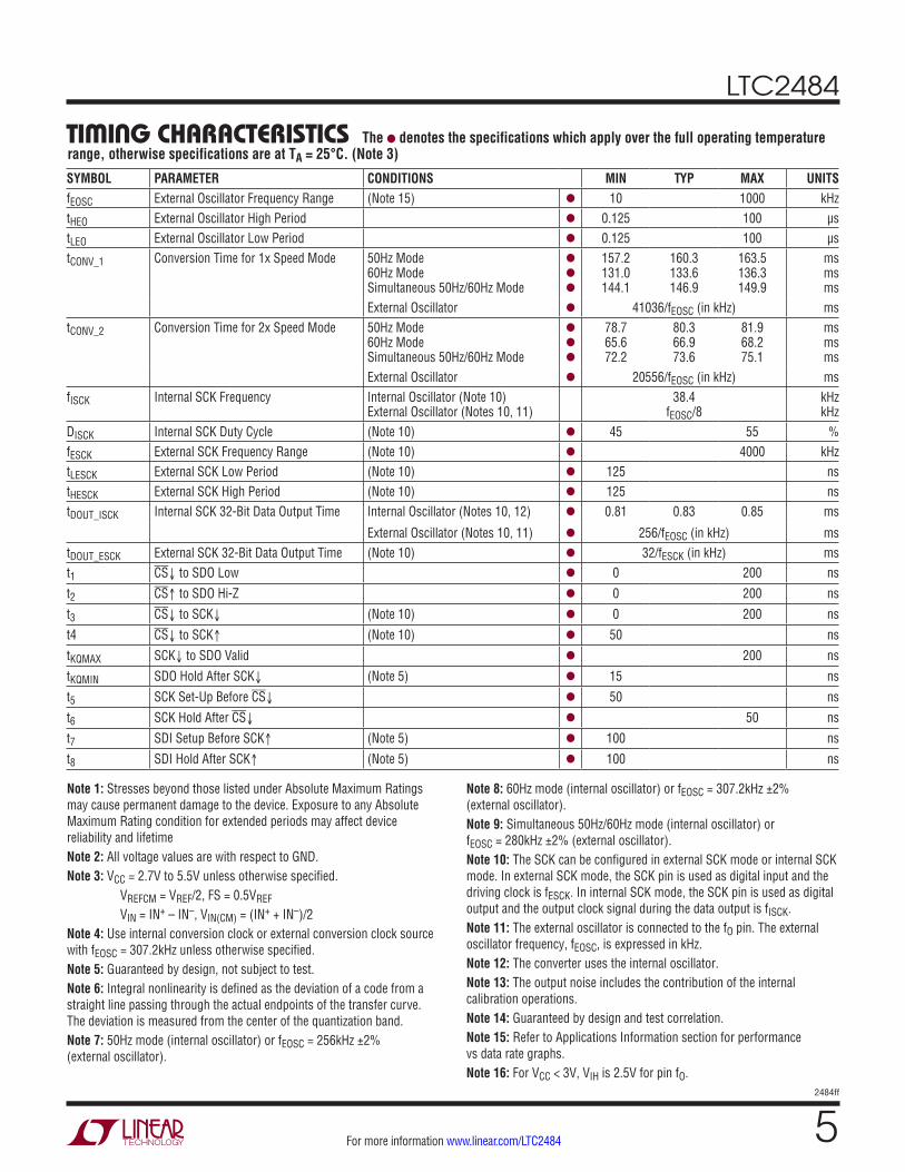
TiMing characTerisTics The l denotes the specifications which apply over the full operating temperature range, otherwise specifications are at TA = 25°C. (Note 3)
SYMBOL PARAMETER CONDITIONS MIN TYP MAX UNITSfEOSC External Oscillator Frequency Range (Note 15) l 10 1000 kHztHEO External Oscillator High Period l 0.125 100 µstLEO External Oscillator Low Period l 0.125 100 µstCONV_1 Conversion Time for 1x Speed Mode 50Hz Mode
60Hz Mode Simultaneous 50Hz/60Hz Mode
l
l
l
157.2 131.0 144.1
160.3 133.6 146.9
163.5 136.3 149.9
ms ms ms
External Oscillator l 41036/fEOSC (in kHz) mstCONV_2 Conversion Time for 2x Speed Mode 50Hz Mode
60Hz Mode Simultaneous 50Hz/60Hz Mode
l
l
l
78.7 65.6 72.2
80.3 66.9 73.6
81.9 68.2 75.1
ms ms ms
External Oscillator l 20556/fEOSC (in kHz) msfISCK Internal SCK Frequency Internal Oscillator (Note 10)
External Oscillator (Notes 10, 11)38.4
fEOSC/8kHz kHz
DISCK Internal SCK Duty Cycle (Note 10) l 45 55 %fESCK External SCK Frequency Range (Note 10) l 4000 kHztLESCK External SCK Low Period (Note 10) l 125 nstHESCK External SCK High Period (Note 10) l 125 nstDOUT_ISCK Internal SCK 32-Bit Data Output Time Internal Oscillator (Notes 10, 12) l 0.81 0.83 0.85 ms
External Oscillator (Notes 10, 11) l 256/fEOSC (in kHz) mstDOUT_ESCK External SCK 32-Bit Data Output Time (Note 10) l 32/fESCK (in kHz) mst1 CS↓ to SDO Low l 0 200 ns
t2 CS↑ to SDO Hi-Z l 0 200 ns
t3 CS↓ to SCK↓ (Note 10) l 0 200 ns
t4 CS↓ to SCK↑ (Note 10) l 50 ns
tKQMAX SCK↓ to SDO Valid l 200 ns
tKQMIN SDO Hold After SCK↓ (Note 5) l 15 ns
t5 SCK Set-Up Before CS↓ l 50 ns
t6 SCK Hold After CS↓ l 50 ns
t7 SDI Setup Before SCK↑ (Note 5) l 100 ns
t8 SDI Hold After SCK↑ (Note 5) l 100 ns
Note 1: Stresses beyond those listed under Absolute Maximum Ratings may cause permanent damage to the device. Exposure to any Absolute Maximum Rating condition for extended periods may affect device reliability and lifetimeNote 2: All voltage values are with respect to GND.Note 3: VCC = 2.7V to 5.5V unless otherwise specified. VREFCM = VREF/2, FS = 0.5VREF
VIN = IN+ – IN–, VIN(CM) = (IN+ + IN–)/2Note 4: Use internal conversion clock or external conversion clock source with fEOSC = 307.2kHz unless otherwise specified.Note 5: Guaranteed by design, not subject to test.Note 6: Integral nonlinearity is defined as the deviation of a code from a straight line passing through the actual endpoints of the transfer curve. The deviation is measured from the center of the quantization band. Note 7: 50Hz mode (internal oscillator) or fEOSC = 256kHz ±2% (external oscillator).
Note 8: 60Hz mode (internal oscillator) or fEOSC = 307.2kHz ±2% (external oscillator).Note 9: Simultaneous 50Hz/60Hz mode (internal oscillator) or fEOSC = 280kHz ±2% (external oscillator).Note 10: The SCK can be configured in external SCK mode or internal SCK mode. In external SCK mode, the SCK pin is used as digital input and the driving clock is fESCK. In internal SCK mode, the SCK pin is used as digital output and the output clock signal during the data output is fISCK.Note 11: The external oscillator is connected to the fO pin. The external oscillator frequency, fEOSC, is expressed in kHz.Note 12: The converter uses the internal oscillator.Note 13: The output noise includes the contribution of the internal calibration operations.Note 14: Guaranteed by design and test correlation.Note 15: Refer to Applications Information section for performance vs data rate graphs.Note 16: For VCC < 3V, VIH is 2.5V for pin fO.
LTC2484
62484ff
For more information www.linear.com/LTC2484
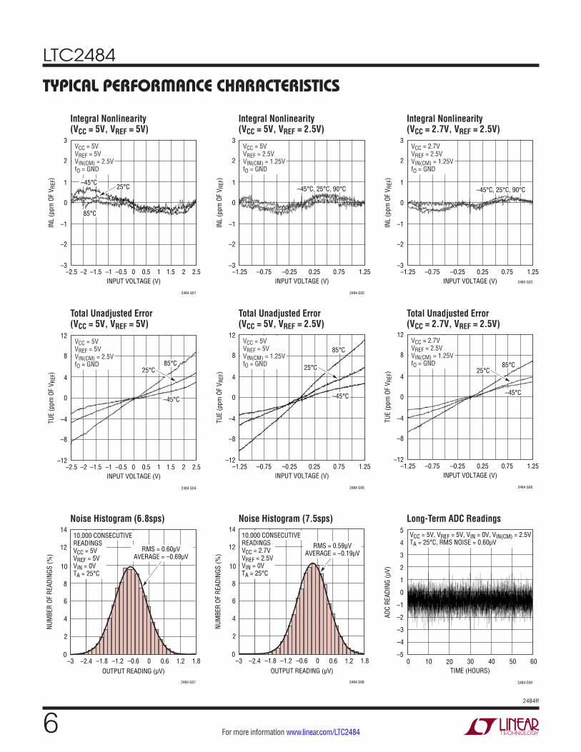
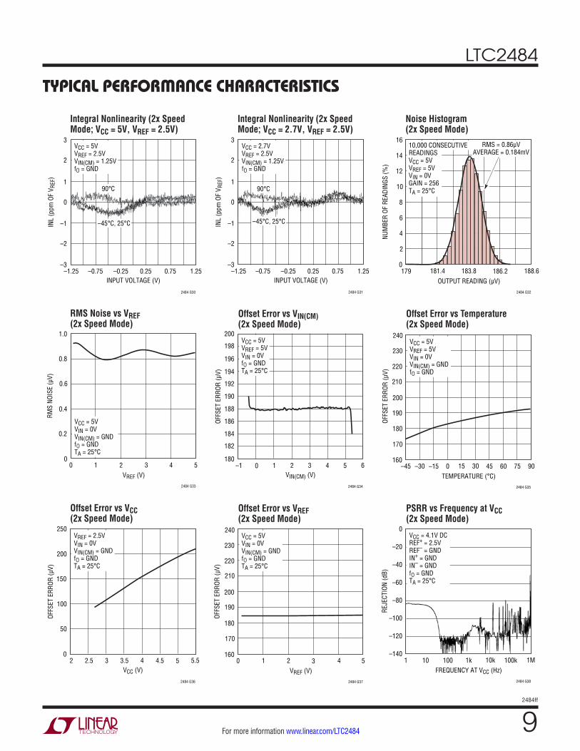
Typical perForMance characTerisTics
Integral Nonlinearity (VCC = 5V, VREF = 5V)
Integral Nonlinearity (VCC = 5V, VREF = 2.5V)
Integral Nonlinearity (VCC = 2.7V, VREF = 2.5V)
Total Unadjusted Error (VCC = 5V, VREF = 5V)
Total Unadjusted Error (VCC = 5V, VREF = 2.5V)
Total Unadjusted Error (VCC = 2.7V, VREF = 2.5V)
Noise Histogram (6.8sps) Noise Histogram (7.5sps) Long-Term ADC Readings
INPUT VOLTAGE (V)
–3
INL
(ppm
OF
V REF
)
–1
1
3
–2
0
2
–1.5 –0.5 0.5 1.5
2484 G01
2.5–2–2.5 –1 0 1 2
VCC = 5VVREF = 5VVIN(CM) = 2.5VfO = GND
85°C
–45°C25°C
INPUT VOLTAGE (V)
–3
INL
(ppm
OF
V REF
)–1
1
3
–2
0
2
–0.75 –0.25 0.25 0.75
2484 G02
1.25–1.25
VCC = 5VVREF = 2.5VVIN(CM) = 1.25VfO = GND
–45°C, 25°C, 90°C
INPUT VOLTAGE (V)
–3
INL
(ppm
OF
V REF
)
–1
1
3
–2
0
2
–0.75 –0.25 0.25 0.752484 G03
1.25–1.25
VCC = 2.7VVREF = 2.5VVIN(CM) = 1.25VfO = GND
–45°C, 25°C, 90°C
INPUT VOLTAGE (V)
–12
TUE
(ppm
OF
V REF
)
–4
4
12
–8
0
8
–1.5 –0.5 0.5 1.5
2484 G04
2.5–2–2.5 –1 0 1 2
VCC = 5VVREF = 5VVIN(CM) = 2.5VfO = GND 85°C
25°C
–45°C
INPUT VOLTAGE (V)
–12
TUE
(ppm
OF
V REF
)
–4
4
12
–8
0
8
–0.75 –0.25 0.25 0.75
2484 G05
1.25–1.25
VCC = 5VVREF = 5VVIN(CM) = 1.25VfO = GND
85°C
25°C
–45°C
INPUT VOLTAGE (V)
–12
TUE
(ppm
OF
V REF
)
–4
4
12
–8
0
8
–0.75 –0.25 0.25 0.75
2484 G06
1.25–1.25
VCC = 2.7VVREF = 2.5VVIN(CM) = 1.25VfO = GND 85°C
25°C
–45°C
OUTPUT READING (µV)–3
NUM
BER
OF R
EADI
NGS
(%)
8
10
12
0.6
2484 G07
6
4
–1.8 –0.6–2.4 1.2–1.2 0 1.8
2
0
1410,000 CONSECUTIVEREADINGSVCC = 5VVREF = 5VVIN = 0VTA = 25°C
RMS = 0.60µVAVERAGE = –0.69µV
OUTPUT READING (µV)–3
NUM
BER
OF R
EADI
NGS
(%)
8
10
12
0.6
2484 G08
6
4
–1.8 –0.6–2.4 1.2–1.2 0 1.8
2
0
1410,000 CONSECUTIVEREADINGSVCC = 2.7VVREF = 2.5VVIN = 0VTA = 25°C
RMS = 0.59µVAVERAGE = –0.19µV
TIME (HOURS)0
–5
ADC
READ
ING
(µV)
–3
–1
1
10 20 30 40
2484 G09
50
3
5
–4
–2
0
2
4
60
VCC = 5V, VREF = 5V, VIN = 0V, VIN(CM) = 2.5VTA = 25°C, RMS NOISE = 0.60µV
LTC2484
72484ff
For more information www.linear.com/LTC2484
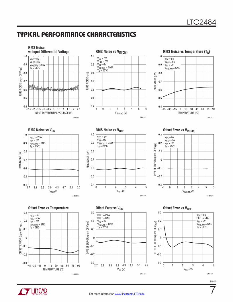
Typical perForMance characTerisTics
RMS Noise vs Input Differential Voltage RMS Noise vs VIN(CM) RMS Noise vs Temperature (TA)
RMS Noise vs VCC RMS Noise vs VREF Offset Error vs VIN(CM)
Offset Error vs Temperature Offset Error vs VCC Offset Error vs VREF
INPUT DIFFERENTIAL VOLTAGE (V)
0.4
RMS
NOIS
E (p
pm O
F V R
EF)
0.6
0.8
1.0
0.5
0.7
0.9
–1.5 –0.5 0.5 1.5
2484 G10
2.5–2–2.5 –1 0 1 2
VCC = 5VVREF = 5VVIN(CM) = 2.5VTA = 25°C
VIN(CM) (V)–1
RMS
NOIS
E (µ
V) 0.8
0.9
1.0
2 4
2484 G11
0.7
0.6
0 1 3 5 6
0.5
0.4
VCC = 5VVREF = 5VVIN = 0VVIN(CM) = GNDTA = 25°C
TEMPERATURE (°C)–45
0.4
RMS
NOIS
E (µ
V)
0.5
0.6
0.7
0.8
1.0
–30 –15 150 30 45 60
2484 G12
75 90
0.9
VCC = 5VVREF = 5VVIN = 0VVIN(CM) = GND
VCC (V)2.7
RMS
NOIS
E (µ
V) 0.8
0.9
1.0
3.9 4.7
2484 G13
0.7
0.6
3.1 3.5 4.3 5.1 5.5
0.5
0.4
VREF = 2.5VVIN = 0VVIN(CM) = GNDTA = 25°C
VREF (V)0
0.4
RMS
NOIS
E (µ
V)
0.5
0.6
0.7
0.8
0.9
1.0
1 2 3 4
2484 G14
5
VCC = 5VVIN = 0VVIN(CM) = GNDTA = 25°C
VIN(CM) (V)–1
OFFS
ET E
RROR
(ppm
OF
V REF
)0.1
0.2
0.3
2 4
2484 G15
0
–0.1
0 1 3 5 6
–0.2
–0.3
VCC = 5VVREF = 5VVIN = 0VTA = 25°C
TEMPERATURE (°C)–45
–0.3
OFFS
ET E
RROR
(ppm
OF
V REF
)
–0.2
0
0.1
0.2
–15 15 30 90
2484 G16
–0.1
–30 0 45 60 75
0.3VCC = 5VVREF = 5VVIN = 0VVIN(CM) = GNDfO = GND
VCC (V)2.7
OFFS
ET E
RROR
(ppm
OF
V REF
)
0.1
0.2
0.3
3.9 4.7
2484 G17
0
–0.1
3.1 3.5 4.3 5.1 5.5
–0.2
–0.3
REF+ = 2.5VREF– = GNDVIN = 0VVIN(CM) = GNDTA = 25°C
VREF (V)0
–0.3
OFFS
ET E
RROR
(ppm
OF
V REF
)
–0.2
–0.1
0
0.1
0.2
0.3
1 2 3 4
2484 G18
5
VCC = 5VREF– = GNDVIN = 0VVIN(CM) = GNDTA = 25°C
LTC2484
82484ff
For more information www.linear.com/LTC2484
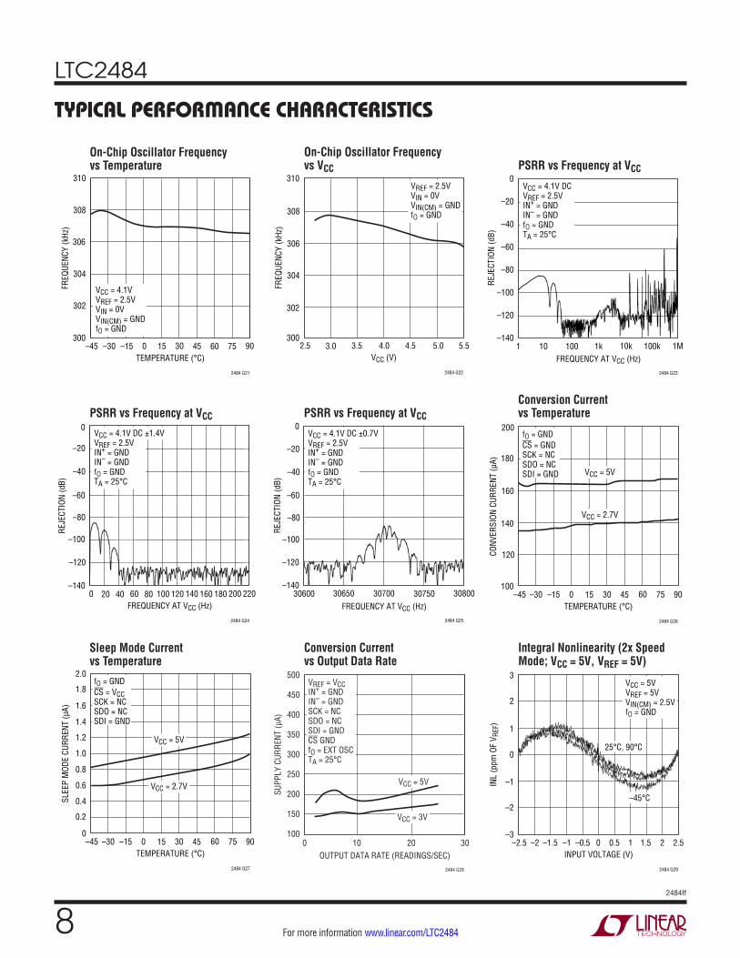
Typical perForMance characTerisTics
On-Chip Oscillator Frequency vs Temperature
On-Chip Oscillator Frequency vs VCC PSRR vs Frequency at VCC
PSRR vs Frequency at VCC PSRR vs Frequency at VCC
Conversion Current vs Temperature
Sleep Mode Current vs Temperature
TEMPERATURE (°C)–45 –30
300
FREQ
UENC
Y (k
Hz)
304
310
–15 30 45
2484 G21
302
308
306
150 60 75 90
VCC = 4.1VVREF = 2.5VVIN = 0VVIN(CM) = GNDfO = GND
VCC (V)2.5
300
FREQ
UENC
Y (k
Hz)
302
304
306
308
310
3.0 3.5 4.0 4.5
2484 G22
5.0 5.5
VREF = 2.5VVIN = 0VVIN(CM) = GNDfO = GND
FREQUENCY AT VCC (Hz)1
0
–20
–40
–60
–80
–100
–120
–1401k 100k
2484 G23
10 100 10k 1M
REJE
CTIO
N (d
B)
VCC = 4.1V DCVREF = 2.5VIN+ = GNDIN– = GNDfO = GNDTA = 25°C
FREQUENCY AT VCC (Hz)0
–140
REJE
CTIO
N (d
B)
–120
–80
–60
–40
0
20 100 140
2484 G24
–100
–20
80 180 22020040 60 120 160
VCC = 4.1V DC ±1.4VVREF = 2.5VIN+ = GNDIN– = GNDfO = GNDTA = 25°C
FREQUENCY AT VCC (Hz)30600
–60
–40
0
30750
2484 G25
–80
–100
30650 30700 30800
–120
–140
–20
REJE
CTIO
N (d
B)
VCC = 4.1V DC ±0.7VVREF = 2.5VIN+ = GNDIN– = GNDfO = GNDTA = 25°C
TEMPERATURE (°C)–45
100
CONV
ERSI
ON C
URRE
NT (µ
A)
120
160
180
200
–15 15 30 90
2484 G26
140
–30 0 45 60 75
VCC = 5V
VCC = 2.7V
fO = GNDCS = GNDSCK = NCSDO = NCSDI = GND
TEMPERATURE (°C)–45
0
SLEE
P M
ODE
CURR
ENT
(µA)
0.2
0.6
0.8
1.0
2.0
1.4
–15 15 30 90
2484 G27
0.4
1.6
1.8
1.2
–30 0 45 60 75
VCC = 5V
VCC = 2.7V
fO = GNDCS = VCCSCK = NCSDO = NCSDI = GND
Conversion Current vs Output Data Rate
Integral Nonlinearity (2x Speed Mode; VCC = 5V, VREF = 5V)
OUTPUT DATA RATE (READINGS/SEC)0
SUPP
LY C
URRE
NT (µ
A)
500
450
400
350
300
250
200
150
100
2484 G28
20 3010
VCC = 5V
VCC = 3V
VREF = VCCIN+ = GNDIN– = GNDSCK = NCSDO = NCSDI = GNDCS GNDfO = EXT OSCTA = 25°C
INPUT VOLTAGE (V)
–3
INL
(ppm
OF
V REF
)
–1
1
3
–2
0
2
–1.5 –0.5 0.5 1.5
2484 G29
2.5–2–2.5 –1 0 1 2
VCC = 5VVREF = 5VVIN(CM) = 2.5VfO = GND
25°C, 90°C
–45°C
LTC2484
92484ff
For more information www.linear.com/LTC2484
Typical perForMance characTerisTics
Integral Nonlinearity (2x Speed Mode; VCC = 5V, VREF = 2.5V)
Integral Nonlinearity (2x Speed Mode; VCC = 2.7V, VREF = 2.5V)
Noise Histogram (2x Speed Mode)
Offset Error vs VIN(CM) (2x Speed Mode)
Offset Error vs Temperature (2x Speed Mode)
INPUT VOLTAGE (V)
–3
INL
(ppm
OF
V REF
)
–1
1
3
–2
0
2
–0.75 –0.25 0.25 0.75
2484 G30
1.25–1.25
VCC = 5VVREF = 2.5VVIN(CM) = 1.25VfO = GND
90°C
–45°C, 25°C
INPUT VOLTAGE (V)
–3
INL
(ppm
OF
V REF
)–1
1
3
–2
0
2
–0.75 –0.25 0.25 0.75
2484 G31
1.25–1.25
VCC = 2.7VVREF = 2.5VVIN(CM) = 1.25VfO = GND
90°C
–45°C, 25°C
OUTPUT READING (µV)179
NUM
BER
OF R
EADI
NGS
(%)
8
10
12
186.2
2484 G32
6
4
181.4 183.8 188.6
2
0
16
14
10,000 CONSECUTIVEREADINGSVCC = 5VVREF = 5VVIN = 0VGAIN = 256TA = 25°C
RMS = 0.86µVAVERAGE = 0.184mV
RMS Noise vs VREF (2x Speed Mode)
VREF (V)0
RMS
NOIS
E (µ
V)
0.6
0.8
1.0
4
2484 G33
0.4
0.2
01 2 3 5
VCC = 5VVIN = 0VVIN(CM) = GNDfO = GNDTA = 25°C
VIN(CM) (V)–1
180
OFFS
ET E
RROR
(µV)
182
186
188
190
200
194
1 3 4
2484 G34
184
196
198
192
0 2 5 6
VCC = 5VVREF = 5VVIN = 0VfO = GNDTA = 25°C
TEMPERATURE (°C)–45
OFFS
ET E
RROR
(µV)
200
210
220
75
2484 G35
190
180
160–15 15 45–30 900 30 60
170
240
230VCC = 5VVREF = 5VVIN = 0VVIN(CM) = GNDfO = GND
Offset Error vs VCC (2x Speed Mode)
Offset Error vs VREF (2x Speed Mode)
PSRR vs Frequency at VCC (2x Speed Mode)
VCC (V)2 2.5
0
OFFS
ET E
RROR
(µV)
100
250
3 4 4.5
2484 G36
50
200
150
3.5 5 5.5
VREF = 2.5VVIN = 0VVIN(CM) = GNDfO = GNDTA = 25°C
VREF (V)0
OFFS
ET E
RROR
(µV)
190
200
210
3 5
2484 G37
180
170
1601 2 4
220
230
240VCC = 5VVIN = 0VVIN(CM) = GNDfO = GNDTA = 25°C
FREQUENCY AT VCC (Hz)1
0
–20
–40
–60
–80
–100
–120
–1401k 100k
2484 G38
10 100 10k 1M
REJE
CTIO
N (d
B)
VCC = 4.1V DCREF+ = 2.5VREF– = GNDIN+ = GNDIN– = GNDfO = GNDTA = 25°C
LTC2484
102484ff
For more information www.linear.com/LTC2484
Typical perForMance characTerisTics
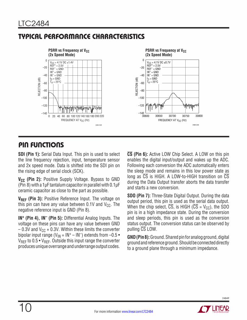
PSRR vs Frequency at VCC (2x Speed Mode)
PSRR vs Frequency at VCC (2x Speed Mode)
FREQUENCY AT VCC (Hz)0
–140
REJE
CTIO
N (d
B)
–120
–80
–60
–40
0
20 100 140
2484 G39
–100
–20
80 180 22020040 60 120 160
VCC = 4.1V DC ±1.4VREF+ = 2.5VREF– = GNDIN+ = GNDIN– = GNDfO = GNDTA = 25°C
FREQUENCY AT VCC (Hz)30600
–60
–40
0
30750
2484 G40
–80
–100
30650 30700 30800
–120
–140
–20
REJE
CTIO
N (d
B)
VCC = 4.1V DC ±0.7VREF+ = 2.5VREF– = GNDIN+ = GNDIN– = GNDfO = GNDTA = 25°C
pin FuncTionsSDI (Pin 1): Serial Data Input. This pin is used to select the line frequency rejection, input, temperature sensor and 2x speed mode. Data is shifted into the SDI pin on the rising edge of serial clock (SCK).
VCC (Pin 2): Positive Supply Voltage. Bypass to GND (Pin 8) with a 1µF tantalum capacitor in parallel with 0.1µF ceramic capacitor as close to the part as possible.
VREF (Pin 3): Positive Reference Input. The voltage on this pin can have any value between 0.1V and VCC. The negative reference input is GND (Pin 8).
IN+ (Pin 4), IN– (Pin 5): Differential Analog Inputs. The voltage on these pins can have any value between GND – 0.3V and VCC + 0.3V. Within these limits the converter bipolar input range (VIN = IN+ – IN–) extends from –0.5 • VREF to 0.5 • VREF . Outside this input range the converter produces unique overrange and underrange output codes.
CS (Pin 6): Active LOW Chip Select. A LOW on this pin enables the digital input/output and wakes up the ADC. Following each conversion the ADC automatically enters the sleep mode and remains in this low power state as long as CS is HIGH. A LOW-to-HIGH transition on CS during the Data Output transfer aborts the data transfer and starts a new conversion.
SDO (Pin 7): Three-State Digital Output. During the data output period, this pin is used as the serial data output. When the chip select, CS, is HIGH (CS = VCC), the SDO pin is in a high impedance state. During the conversion and sleep periods, this pin is used as the conversion status output. The conversion status can be observed by pulling CS LOW.
GND (Pin 8): Ground. Shared pin for analog ground, digital ground and reference ground. Should be connected directly to a ground plane through a minimum impedance.
LTC2484
112484ff
For more information www.linear.com/LTC2484
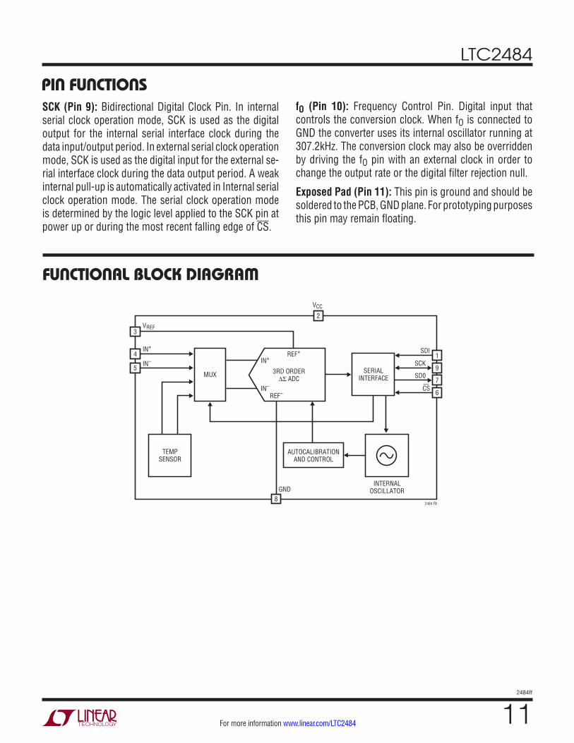
pin FuncTionsSCK (Pin 9): Bidirectional Digital Clock Pin. In internal serial clock operation mode, SCK is used as the digital output for the internal serial interface clock during the data input/output period. In external serial clock operation mode, SCK is used as the digital input for the external se-rial interface clock during the data output period. A weak internal pull-up is automatically activated in Internal serial clock operation mode. The serial clock operation mode is determined by the logic level applied to the SCK pin at power up or during the most recent falling edge of CS.
fO (Pin 10): Frequency Control Pin. Digital input that controls the conversion clock. When fO is connected to GND the converter uses its internal oscillator running at 307.2kHz. The conversion clock may also be overridden by driving the fO pin with an external clock in order to change the output rate or the digital filter rejection null.
Exposed Pad (Pin 11): This pin is ground and should be soldered to the PCB, GND plane. For prototyping purposes this pin may remain floating.
FuncTional block DiagraM
1
9
4
5
8
7
6
3RD ORDER∆Σ ADC
REF+
IN+IN+
3
2VREF
VCC
GND
IN–
IN–
REF–
SERIALINTERFACE
TEMPSENSOR
MUX
SDI
CS
2484 FB
SCK
SD0
AUTOCALIBRATIONAND CONTROL
INTERNALOSCILLATOR
LTC2484
122484ff
For more information www.linear.com/LTC2484
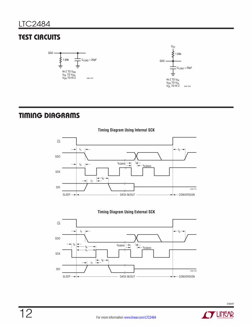
TiMing DiagraMs
Timing Diagram Using Internal SCK
CS
SDO
SCK
SDI
t1
t3
t7t8
SLEEP
tKQMAX
CONVERSIONDATA IN/OUT
tKQMIN
t2
2484 TD1
Timing Diagram Using External SCK
CS
SDO
SCK
SDI
t1
t5t6t4
t7t8
SLEEP
tKQMAX
CONVERSIONDATA IN/OUT
tKQMIN
t2
2484 TD2
TesT circuiTs
1.69k
SDO
2484 TC01
Hi-Z TO VOHVOL TO VOHVOH TO Hi-Z
CLOAD = 20pF
1.69k
SDO
2484 TC02
Hi-Z TO VOLVOH TO VOLVOL TO Hi-Z
CLOAD = 20pF
VCC
LTC2484
132484ff
For more information www.linear.com/LTC2484
applicaTions inForMaTionCONVERTER OPERATION
Converter Operation Cycle
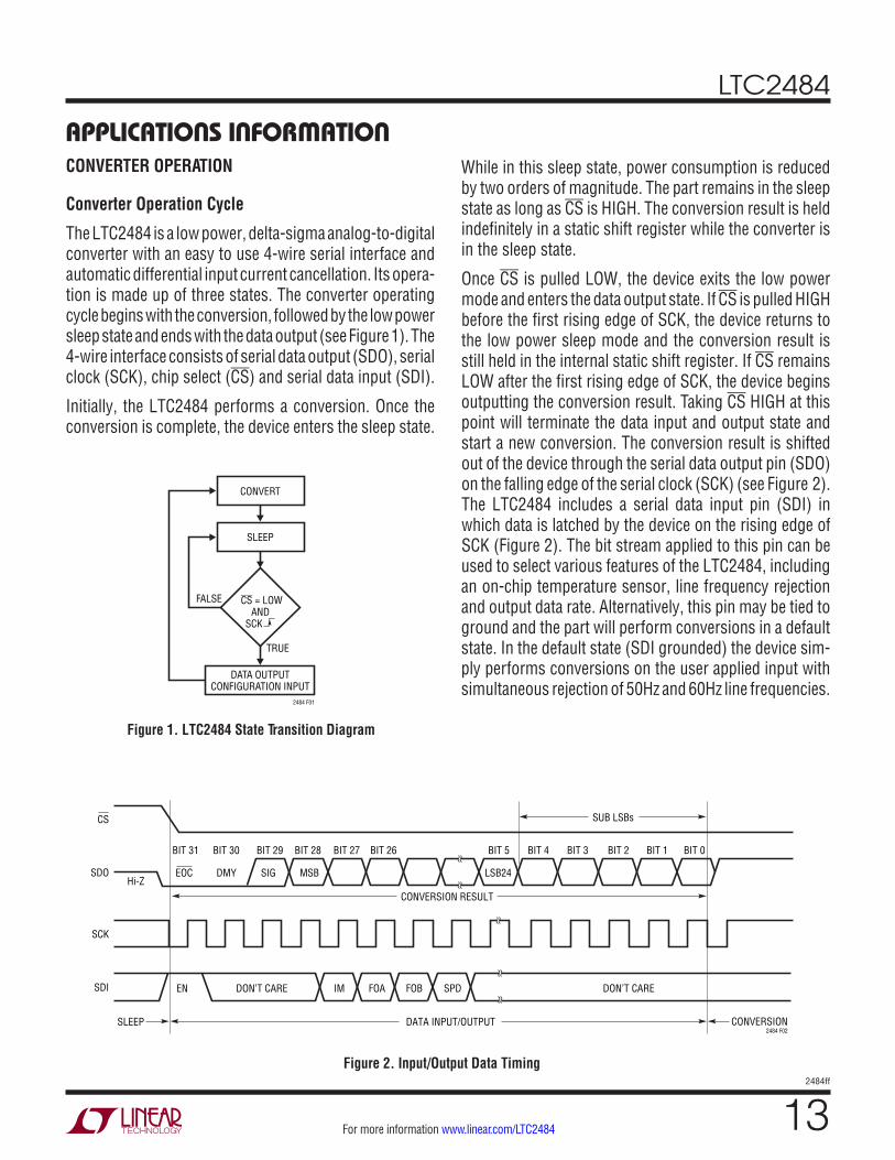
The LTC2484 is a low power, delta-sigma analog-to-digital converter with an easy to use 4-wire serial interface and automatic differential input current cancellation. Its opera-tion is made up of three states. The converter operating cycle begins with the conversion, followed by the low power sleep state and ends with the data output (see Figure 1). The 4-wire interface consists of serial data output (SDO), serial clock (SCK), chip select (CS) and serial data input (SDI).
Initially, the LTC2484 performs a conversion. Once the conversion is complete, the device enters the sleep state.
CONVERT
SLEEP
DATA OUTPUTCONFIGURATION INPUT
2484 F01
TRUE
FALSE CS = LOW ANDSCK
Figure 1. LTC2484 State Transition Diagram
CS
SDOHi-Z
SIGDMY
BIT 29
MSB
CONVERSION RESULT
BIT 28 BIT 27 BIT 26
LSB24
BIT 4BIT 5 BIT 3 BIT 1 BIT 0BIT 2BIT 30
SCK
SDI
SLEEP DATA INPUT/OUTPUT
BIT 31
EOC
EN DON’T CARE IM FOBFOA SPD DON’T CARE
CONVERSION2484 F02
SUB LSBs
Figure 2. Input/Output Data Timing
While in this sleep state, power consumption is reduced by two orders of magnitude. The part remains in the sleep state as long as CS is HIGH. The conversion result is held indefinitely in a static shift register while the converter is in the sleep state.
Once CS is pulled LOW, the device exits the low power mode and enters the data output state. If CS is pulled HIGH before the first rising edge of SCK, the device returns to the low power sleep mode and the conversion result is still held in the internal static shift register. If CS remains LOW after the first rising edge of SCK, the device begins outputting the conversion result. Taking CS HIGH at this point will terminate the data input and output state and start a new conversion. The conversion result is shifted out of the device through the serial data output pin (SDO) on the falling edge of the serial clock (SCK) (see Figure 2). The LTC2484 includes a serial data input pin (SDI) in which data is latched by the device on the rising edge of SCK (Figure 2). The bit stream applied to this pin can be used to select various features of the LTC2484, including an on-chip temperature sensor, line frequency rejection and output data rate. Alternatively, this pin may be tied to ground and the part will perform conversions in a default state. In the default state (SDI grounded) the device sim-ply performs conversions on the user applied input with simultaneous rejection of 50Hz and 60Hz line frequencies.
LTC2484
142484ff
For more information www.linear.com/LTC2484
applicaTions inForMaTionThrough timing control of the CS and SCK pins, the LTC2484 offers several flexible modes of operation (internal or external SCK and free-running conversion modes). These various modes do not require programming configuration registers; moreover, they do not disturb the cyclic operation described above. These modes of operation are described in detail in the Serial Interface Timing Modes section.
Easy Drive Input Current Cancellation
The LTC2484 combines a high precision delta-sigma ADC with an automatic differential input current cancellation front end. A proprietary front-end passive sampling net-work transparently removes the differential input current. This enables external RC networks and high impedance sensors to directly interface to the LTC2484 without external amplifiers. The remaining common mode input current is eliminated by either balancing the differential input impedances or setting the common mode input equal to the common mode reference (see Automatic Input Current Cancellation section). This unique architecture does not require on-chip buffers enabling input signals to swing all the way to ground and up to VCC. Furthermore, the cancellation does not interfere with the transparent offset and full-scale auto-calibration and the absolute accuracy (full-scale + offset + linearity) is maintained with external RC networks.
Accessing the Special Features of the LTC2484
The LTC2484 combines a high resolution, low noise ∆Σ analog-to-digital converter with an on-chip selectable temperature sensor, programmable digital filter and output rate control. These special features are selected through a
single 8-bit serial input word during the data input/output cycle (see Figure 2).
The LTC2484 powers up in a default mode commonly used for most measurements. The device will remain in this mode as long as the serial data input (SDI) is low. In this default mode, the measured input is external, the digital filter simultaneously rejects 50Hz and 60Hz line frequency noise, and the speed mode is 1x (offset automatically, continuously calibrated).
A simple serial interface grants access to any or all special functions contained within the LTC2484. In order to change the mode of operation, an enable bit (EN) followed by up to 7 bits of data are shifted into the device (see Table 1). The first 3 bits, in order to remain pin-compatible with the LTC2480, are don’t-cares and can be either HIGH or LOW. The 4th bit (IM) is used to select the internal temperature sensor as the conversion input, while the 5th and 6th bits (FA, FB) combine to determine the line frequency rejection mode. The 7th bit (SPD) is used to double the output rate by disabling the offset auto calibration.
Temperature Sensor (IM)
The LTC2484 includes an on-chip temperature sensor. The temperature sensor is selected by setting IM = 1 in the serial input data stream. Conversions are performed directly on the temperature sensor by the converter. While operating in this mode, the device behaves as a tempera-ture to bits converter. The digital reading is proportional to the absolute temperature of the device. This feature allows the converter to linearize temperature sensors or continuously remove temperature effects from external
Table 1. Selecting Special Modes
EN
2484 TBL1
IM FoA FoB SPD CommentsKeep Previous ModeExternal Input, 50Hz and 60Hz Rejection, AutocalibrationExternal Input, 50Hz Rejection, AutocalibrationExternal Input, 60Hz Rejection, AutocalibrationExternal Input, 50Hz and 60Hz Rejection, 2x SpeedExternal Input, 50Hz Rejection, 2x SpeedExternal Input, 60Hz Rejection, 2x SpeedTemperature Input, 50Hz and 60Hz Rejection, AutocalibrationTemperature Input, 50Hz Rejection, AutocalibrationTemperature Input, 60Hz Rejection, AutocalibrationReserved, Do Not Use
01111111111
X000000111X
X000111XXXX
X0100100101
X0010010011
LTC2484
152484ff
For more information www.linear.com/LTC2484
applicaTions inForMaTionsensors. Several applications leveraging this feature are presented in more detail in the applications section. While operating in this mode, the speed is set to normal independent of control bit SPD.
Rejection Mode (FA, FB)
The LTC2484 includes a high accuracy on-chip oscilla-tor with no required external components. Coupled with a 4th order digital lowpass filter, the LTC2484 rejects line frequency noise. In the default mode, the LTC2484 simultaneously rejects 50Hz and 60Hz by at least 87dB. The LTC2484 can also be configured to selectively reject 50Hz or 60Hz to better than 110dB.
Speed Mode (SPD)
The LTC2484 continuously performs offset calibrations. Every conversion cycle, two conversions are automatically performed (default) and the results combined. This result is free from offset and drift. In applications where the offset is not critical, the auto-calibration feature can be disabled with the benefit of twice the output rate.
Linearity, full-scale accuracy, full-scale drift are identical for both 2x and 1x speed modes. In both the 1x and 2x speed there is no latency. This enables input steps or multiplexer channel changes to settle in a single conver-sion cycle easing system overhead and increasing the effective conversion rate.
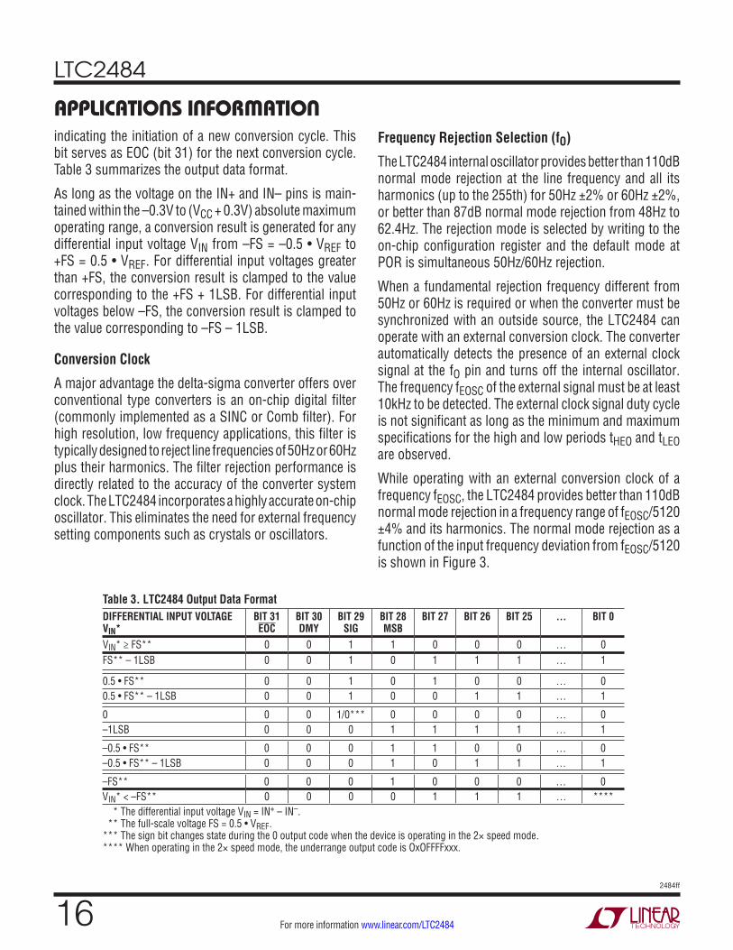
Output Data Format
The LTC2484 serial output data stream is 32 bits long. The first 3 bits represent status information indicating the sign and conversion state. The next 24 bits are the conversion result, MSB first. The remaining 5 bits are sub LSBs below the 24-bit level. The third and fourth bit together are also used to indicate an underrange condition (the differential input voltage is below –FS) or an overrange condition (the differential input voltage is above +FS).
CS may be pulled HIGH prior to outputting all 32 bits, aborting the data out transfer and initiating a new conversion.
Bit 31 (first output bit) is the end of conversion (EOC) indicator. This bit is available at the SDO pin during the conversion and sleep states whenever the CS pin is LOW.
This bit is HIGH during the conversion and goes LOW when the conversion is complete.
Bit 30 (second output bit) is a dummy bit (DMY) and is always LOW.
Bit 29 (third output bit) is the conversion result sign indicator (SIG). If VIN is >0, this bit is HIGH. If VIN is <0, this bit is LOW.
Bit 28 (fourth output bit) is the most significant bit (MSB) of the result. This bit in conjunction with bit 29 also provides the underrange or overrange indication. If both bit 29 and bit 28 are HIGH, the differential input voltage is above +FS. If both bit 29 and bit 28 are LOW, the differential input voltage is below –FS.
The function of these bits is summarized in Table 2.
Table 2. LTC2484 Status Bits INPUT RANGE
BIT 31 EOC
BIT 30 DMY
BIT 29 SIG
BIT 28 MSB
VIN ≥ 0.5 • VREF 0 0 1 1
0V ≤ VIN < 0.5 • VREF 0 0 1/0 0
–0.5 • VREF ≤ VIN < 0V 0 0 0 1
VIN < –0.5 • VREF 0 0 0 0
Bits 28-5 are the 24-bit conversion result MSB first.
Bits 4–0 are sub LSBs below the 24-bit level. Bits 4–0 may be included in averaging or discarded without loss of resolution.
Data is shifted out of the SDO pin under control of the serial clock (SCK) (see Figure 2). Whenever CS is HIGH, SDO remains high impedance and any externally gener-ated SCK clock pulses are ignored by the internal data out shift register.
In order to shift the conversion result out of the device, CS must first be driven LOW. EOC is seen at the SDO pin of the device once CS is pulled LOW. EOC changes in real time from HIGH to LOW at the completion of a conversion. This signal may be used as an interrupt for an external microcontroller. Bit 31 (EOC) can be captured on the first rising edge of SCK. Bit 30 is shifted out of the device on the first falling edge of SCK. The final data bit (bit 0) is shifted out on the falling edge of the 31st SCK and may be latched on the rising edge of the 32nd SCK pulse. On the falling edge of the 32nd SCK pulse, SDO goes HIGH
LTC2484
162484ff
For more information www.linear.com/LTC2484
applicaTions inForMaTionindicating the initiation of a new conversion cycle. This bit serves as EOC (bit 31) for the next conversion cycle. Table 3 summarizes the output data format.
As long as the voltage on the IN+ and IN– pins is main-tained within the –0.3V to (VCC + 0.3V) absolute maximum operating range, a conversion result is generated for any differential input voltage VIN from –FS = –0.5 • VREF to +FS = 0.5 • VREF. For differential input voltages greater than +FS, the conversion result is clamped to the value corresponding to the +FS + 1LSB. For differential input voltages below –FS, the conversion result is clamped to the value corresponding to –FS – 1LSB.
Conversion Clock
A major advantage the delta-sigma converter offers over conventional type converters is an on-chip digital filter (commonly implemented as a SINC or Comb filter). For high resolution, low frequency applications, this filter is typically designed to reject line frequencies of 50Hz or 60Hz plus their harmonics. The filter rejection performance is directly related to the accuracy of the converter system clock. The LTC2484 incorporates a highly accurate on-chip oscillator. This eliminates the need for external frequency setting components such as crystals or oscillators.
Frequency Rejection Selection (fO)
The LTC2484 internal oscillator provides better than 110dB normal mode rejection at the line frequency and all its harmonics (up to the 255th) for 50Hz ±2% or 60Hz ±2%, or better than 87dB normal mode rejection from 48Hz to 62.4Hz. The rejection mode is selected by writing to the on-chip configuration register and the default mode at POR is simultaneous 50Hz/60Hz rejection.
When a fundamental rejection frequency different from 50Hz or 60Hz is required or when the converter must be synchronized with an outside source, the LTC2484 can operate with an external conversion clock. The converter automatically detects the presence of an external clock signal at the fO pin and turns off the internal oscillator. The frequency fEOSC of the external signal must be at least 10kHz to be detected. The external clock signal duty cycle is not significant as long as the minimum and maximum specifications for the high and low periods tHEO and tLEO are observed.
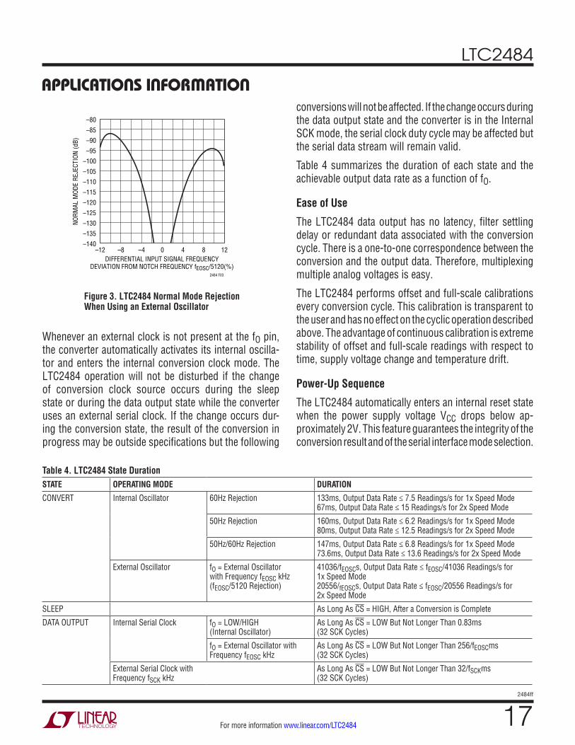
While operating with an external conversion clock of a frequency fEOSC, the LTC2484 provides better than 110dB normal mode rejection in a frequency range of fEOSC/5120 ±4% and its harmonics. The normal mode rejection as a function of the input frequency deviation from fEOSC/5120 is shown in Figure 3.
Table 3. LTC2484 Output Data FormatDIFFERENTIAL INPUT VOLTAGE VIN*
BIT 31 EOC
BIT 30 DMY
BIT 29 SIG
BIT 28 MSB
BIT 27 BIT 26 BIT 25 … BIT 0
VIN* ≥ FS** 0 0 1 1 0 0 0 … 0FS** – 1LSB 0 0 1 0 1 1 1 … 1
0.5 • FS** 0 0 1 0 1 0 0 … 00.5 • FS** – 1LSB 0 0 1 0 0 1 1 … 1
0 0 0 1/0*** 0 0 0 0 … 0–1LSB 0 0 0 1 1 1 1 … 1
–0.5 • FS** 0 0 0 1 1 0 0 … 0–0.5 • FS** – 1LSB 0 0 0 1 0 1 1 … 1
–FS** 0 0 0 1 0 0 0 … 0VIN* < –FS** 0 0 0 0 1 1 1 … **** * The differential input voltage VIN = IN+ – IN–. ** The full-scale voltage FS = 0.5 • VREF . *** The sign bit changes state during the 0 output code when the device is operating in the 2× speed mode . **** When operating in the 2× speed mode, the underrange output code is OxOFFFFxxx.
LTC2484
172484ff
For more information www.linear.com/LTC2484
applicaTions inForMaTion
Whenever an external clock is not present at the fO pin, the converter automatically activates its internal oscilla-tor and enters the internal conversion clock mode. The LTC2484 operation will not be disturbed if the change of conversion clock source occurs during the sleep state or during the data output state while the converter uses an external serial clock. If the change occurs dur-ing the conversion state, the result of the conversion in progress may be outside specifications but the following
conversions will not be affected. If the change occurs during the data output state and the converter is in the Internal SCK mode, the serial clock duty cycle may be affected but the serial data stream will remain valid.
Table 4 summarizes the duration of each state and the achievable output data rate as a function of fO.
Ease of Use
The LTC2484 data output has no latency, filter settling delay or redundant data associated with the conversion cycle. There is a one-to-one correspondence between the conversion and the output data. Therefore, multiplexing multiple analog voltages is easy.
The LTC2484 performs offset and full-scale calibrations every conversion cycle. This calibration is transparent to the user and has no effect on the cyclic operation described above. The advantage of continuous calibration is extreme stability of offset and full-scale readings with respect to time, supply voltage change and temperature drift.
Power-Up Sequence
The LTC2484 automatically enters an internal reset state when the power supply voltage VCC drops below ap-proximately 2V. This feature guarantees the integrity of the conversion result and of the serial interface mode selection.
Table 4. LTC2484 State DurationSTATE OPERATING MODE DURATION
CONVERT Internal Oscillator 60Hz Rejection 133ms, Output Data Rate ≤ 7.5 Readings/s for 1x Speed Mode 67ms, Output Data Rate ≤ 15 Readings/s for 2x Speed Mode
50Hz Rejection 160ms, Output Data Rate ≤ 6.2 Readings/s for 1x Speed Mode 80ms, Output Data Rate ≤ 12.5 Readings/s for 2x Speed Mode
50Hz/60Hz Rejection 147ms, Output Data Rate ≤ 6.8 Readings/s for 1x Speed Mode 73.6ms, Output Data Rate ≤ 13.6 Readings/s for 2x Speed Mode
External Oscillator fO = External Oscillator with Frequency fEOSC kHz (fEOSC/5120 Rejection)
41036/fEOSCs, Output Data Rate ≤ fEOSC/41036 Readings/s for 1x Speed Mode 20556/fEOSCs, Output Data Rate ≤ fEOSC/20556 Readings/s for 2x Speed Mode
SLEEP As Long As CS = HIGH, After a Conversion is Complete
DATA OUTPUT Internal Serial Clock fO = LOW/HIGH (Internal Oscillator)
As Long As CS = LOW But Not Longer Than 0.83ms (32 SCK Cycles)
fO = External Oscillator with Frequency fEOSC kHz
As Long As CS = LOW But Not Longer Than 256/fEOSCms (32 SCK Cycles)
External Serial Clock with Frequency fSCK kHz
As Long As CS = LOW But Not Longer Than 32/fSCKms (32 SCK Cycles)
DIFFERENTIAL INPUT SIGNAL FREQUENCYDEVIATION FROM NOTCH FREQUENCY fEOSC/5120(%)
–12 –8 –4 0 4 8 12
NORM
AL M
ODE
REJE
CTIO
N (d
B)
2484 F03
–80
–85
–90
–95
–100
–105
–110
–115
–120
–125
–130
–135
–140
Figure 3. LTC2484 Normal Mode Rejection When Using an External Oscillator
LTC2484
182484ff
For more information www.linear.com/LTC2484
applicaTions inForMaTionWhen the VCC voltage rises above this critical threshold, the converter creates an internal power-on reset (POR) signal with a duration of approximately 4ms. The POR signal clears all internal registers. Following the POR signal, the LTC2484 starts a normal conversion cycle and follows the succession of states described in Figure 1. The first conversion result following POR is accurate within the specifications of the device if the power supply voltage is restored within the operating range (2.7V to 5.5V) before the end of the POR time interval.
On-Chip Temperature Sensor
The LTC2484 contains an on-chip PTAT (proportional to absolute temperature) signal that can be used as a temperature sensor. The internal PTAT has a typical value of 420mV at 27°C and is proportional to the abso-lute temperature value with a temperature coefficient of 420/(27 + 273) = 1.40mV/°C (SLOPE), as shown in Fig-ure 4. The internal PTAT signal is used in a single-ended mode referenced to device ground internally. The 1x speed mode with automatic offset calibration is automatically selected for the internal PTAT signal measurement as well.
When using the internal temperature sensor, if the output code is normalized to RSDO = VPTAT/VREF , the temperature is calculated using the following formula:
TK =RSDO • VREF
SLOPE in Kelvin
and
TC =RSDO • VREF
SLOPE– 273 in °C
where SLOPE is nominally 1.4mV/°C
Since the PTAT signal can have an initial value variation which results in errors in SLOPE, to achieve better tem-perature measurements, a one-time calibration is needed to adjust the SLOPE value. The converter output of the PTAT signal, R0SDO, is measured at a known temperature T0 (in °C) and the SLOPE is calculated as:
SLOPE =
R0SDO • VREF
T0+ 273
This calibrated SLOPE can be used to calculate the temperature.
If the same VREF source is used during calibration and temperature measurement, the actual value of the VREF is not needed to measure the temperature as shown in the calculation below:
TC =RSDO • VREF
SLOPE– 273
=RSDO
R0SDO• T0+ 273( ) – 273
TEMPERATURE (°C)–60
V PTA
T (m
V)
500
600
120
2484 F04
400
200300 90–30 60
300
VCC = 5VIM = 1fO = GNDSLOPE = 1.40mV/°C
Figure 4. Internal PTAT Signal vs Temperature
Reference Voltage Range
The LTC2484 external reference voltage range is 0.1V to VCC. The converter output noise is determined by the thermal noise of the front-end circuits, and as such, its value in nanovolts is nearly constant with reference voltage. A reduced reference voltage will improve the converter performance when operated with an external conversion clock (external fO signal) at substantially higher output data rates (see the Output Data Rate section). VREF must be ≥1.1V to use the internal temperature sensor.
The negative reference input to the converter is internally tied to GND. GND (Pin 8) should be connected to a ground plane through as short a trace as possible to minimize voltage drop. The LTC2484 has an average operational current of 160µA and for 0.1Ω parasitic resistance, the voltage drop of 16µV causes a gain error of 3.2ppm for VREF = 5V.
LTC2484
192484ff
For more information www.linear.com/LTC2484
applicaTions inForMaTionInput Voltage Range
The analog input is truly differential with an absolute/com-mon mode range for the IN+ and IN– input pins extending from GND – 0.3V to VCC + 0.3V. Outside these limits, the ESD protection devices begin to turn on and the errors due to input leakage current increase rapidly. Within these limits, the LTC2484 converts the bipolar differential input signal, VIN = IN+ – IN–, from –FS to +FS where FS = 0.5 • VREF . Outside this range, the converter indicates the over-range or the underrange condition using distinct output codes. Since the differential input current cancellation does not rely on an on-chip buffer, current cancellation as well as DC performance is maintained rail-to-rail.
Input signals applied to IN+ and IN– pins may extend by 300mV below ground and above VCC. In order to limit any fault current, resistors of up to 5k may be added in series with the IN+ and IN– pins without affecting the performance of the devices. The effect of the series resistance on the converter accuracy can be evaluated from the curves presented in the Input Current/Reference Current sections. In addition, series resistors will introduce a temperature dependent offset error due to the input leakage current. A 1nA input leakage current will develop a 1ppm offset error on a 5k resistor if VREF = 5V. This error has a very strong temperature dependency.
SERIAL INTERFACE TIMING MODES
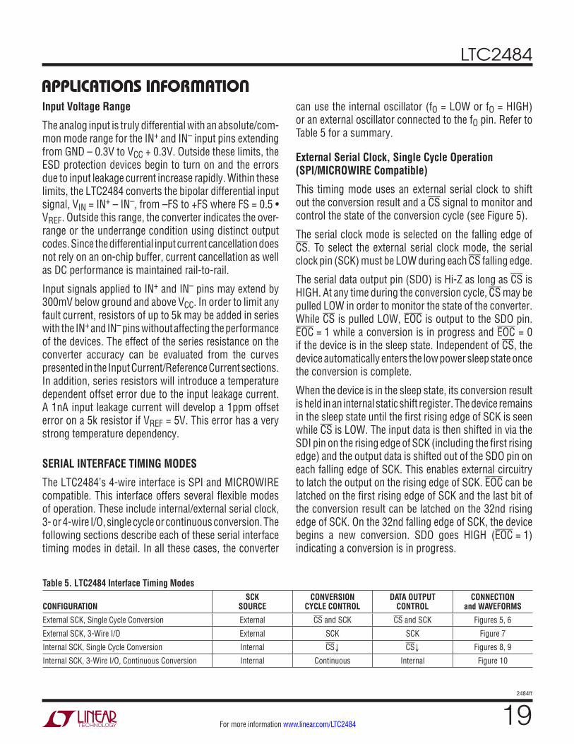
The LTC2484’s 4-wire interface is SPI and MICROWIRE compatible. This interface offers several flexible modes of operation. These include internal/external serial clock, 3- or 4-wire I/O, single cycle or continuous conversion. The following sections describe each of these serial interface timing modes in detail. In all these cases, the converter
can use the internal oscillator (fO = LOW or fO = HIGH) or an external oscillator connected to the fO pin. Refer to Table 5 for a summary.
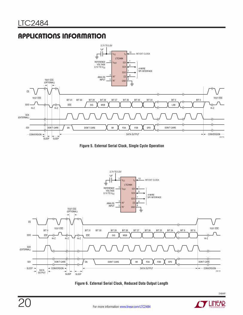
External Serial Clock, Single Cycle Operation (SPI/MICROWIRE Compatible)
This timing mode uses an external serial clock to shift out the conversion result and a CS signal to monitor and control the state of the conversion cycle (see Figure 5).
The serial clock mode is selected on the falling edge of CS. To select the external serial clock mode, the serial clock pin (SCK) must be LOW during each CS falling edge.
The serial data output pin (SDO) is Hi-Z as long as CS is HIGH. At any time during the conversion cycle, CS may be pulled LOW in order to monitor the state of the converter. While CS is pulled LOW, EOC is output to the SDO pin. EOC = 1 while a conversion is in progress and EOC = 0 if the device is in the sleep state. Independent of CS, the device automatically enters the low power sleep state once the conversion is complete.
When the device is in the sleep state, its conversion result is held in an internal static shift register. The device remains in the sleep state until the first rising edge of SCK is seen while CS is LOW. The input data is then shifted in via the SDI pin on the rising edge of SCK (including the first rising edge) and the output data is shifted out of the SDO pin on each falling edge of SCK. This enables external circuitry to latch the output on the rising edge of SCK. EOC can be latched on the first rising edge of SCK and the last bit of the conversion result can be latched on the 32nd rising edge of SCK. On the 32nd falling edge of SCK, the device begins a new conversion. SDO goes HIGH (EOC = 1) indicating a conversion is in progress.
Table 5. LTC2484 Interface Timing Modes
CONFIGURATIONSCK
SOURCECONVERSION
CYCLE CONTROLDATA OUTPUT
CONTROLCONNECTION
and WAVEFORMS
External SCK, Single Cycle Conversion External CS and SCK CS and SCK Figures 5, 6
External SCK, 3-Wire I/O External SCK SCK Figure 7
Internal SCK, Single Cycle Conversion Internal CS↓ CS↓ Figures 8, 9
Internal SCK, 3-Wire I/O, Continuous Conversion Internal Continuous Internal Figure 10
LTC2484
202484ff
For more information www.linear.com/LTC2484
applicaTions inForMaTion
EN DON’T CARE IM FOA FOB SPDSDI DON’T CARE DON’T CARE
SDO
SCK(EXTERNAL)
CS
DATAOUTPUT
CONVERSIONSLEEP
SLEEPSLEEP
TEST EOC
DATA OUTPUT
Hi-Z Hi-ZHi-Z
CONVERSION2484 F06
MSBSIG
BIT 8BIT 27 BIT 26 BIT 25 BIT 24 BIT 9BIT 28BIT 29BIT 30
EOC
BIT 31BIT 0
EOCHi-Z
TEST EOC
TEST EOC (OPTIONAL)
VCC fO
VREF
IN+
IN–
SCK
SDI
SDO
CS
GND
2 10 INT/EXT CLOCK
3
4
5
9
7
8
6
1REFERENCEVOLTAGE
0.1V TO VCC
ANALOGINPUT
1µF
2.7V TO 5.5V
LTC2484
4-WIRESPI INTERFACE
Figure 6. External Serial Clock, Reduced Data Output Length
EOC
BIT 31
SDO
SCK(EXTERNAL)
CS
EN DON’T CARE IM FOA FOB SPDSDI DON’T CARE
TEST EOC
MSBSIG
BIT 0
LSB
BIT 5BIT 27 BIT 26 BIT 25 BIT 24BIT 28BIT 29BIT 30
SLEEPSLEEP
DATA OUTPUT CONVERSION2484 F05
CONVERSION
Hi-ZHi-ZHi-Z
TEST EOC
VCC fO
VREF
IN+
IN–
SCK
SDI
SDO
CS
GND
2 10 INT/EXT CLOCK
3
4
5
9
7
8
6
1REFERENCEVOLTAGE
0.1V TO VCC
ANALOGINPUT
1µF
2.7V TO 5.5V
LTC2484
4-WIRESPI INTERFACE
DON’T CARE
TEST EOC (OPTIONAL)
Figure 5. External Serial Clock, Single Cycle Operation
LTC2484
212484ff
For more information www.linear.com/LTC2484
applicaTions inForMaTionAt the conclusion of the data cycle, CS may remain LOW and EOC monitored as an end-of-conversion interrupt. Alternatively, CS may be driven HIGH setting SDO to Hi-Z. As described above, CS may be pulled LOW at any time in order to monitor the conversion status.
Typically, CS remains LOW during the data output state. However, the data output state may be aborted by pull-ing CS HIGH anytime between the first rising edge and the 32nd falling edge of SCK (see Figure 6). On the rising edge of CS, the device aborts the data output state and immediately initiates a new conversion. If the device has not finished loading the last input bit SPD of SDI by the time CS is pulled HIGH, the SDI information is discarded and the previous configuration is kept. This is useful for systems not requiring all 32 bits of output data, aborting an invalid conversion cycle or synchronizing the start of a conversion.
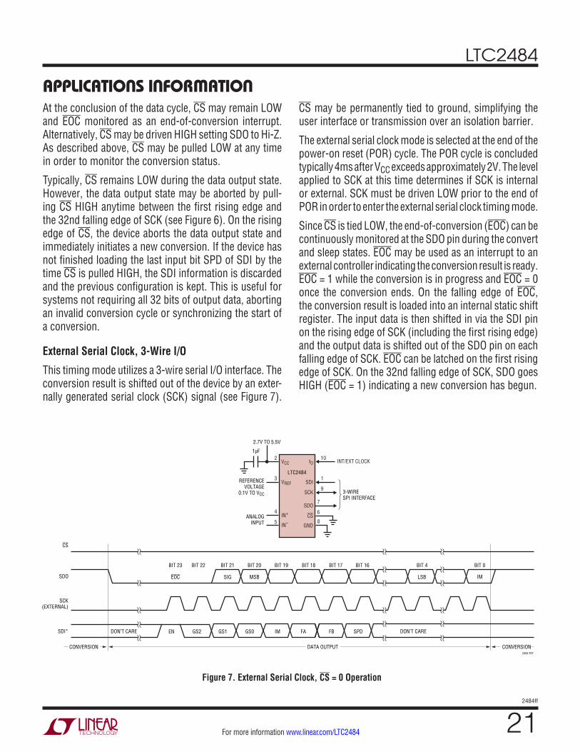
External Serial Clock, 3-Wire I/O
This timing mode utilizes a 3-wire serial I/O interface. The conversion result is shifted out of the device by an exter-nally generated serial clock (SCK) signal (see Figure 7).
CS may be permanently tied to ground, simplifying the user interface or transmission over an isolation barrier.
The external serial clock mode is selected at the end of the power-on reset (POR) cycle. The POR cycle is concluded typically 4ms after VCC exceeds approximately 2V. The level applied to SCK at this time determines if SCK is internal or external. SCK must be driven LOW prior to the end of POR in order to enter the external serial clock timing mode.
Since CS is tied LOW, the end-of-conversion (EOC) can be continuously monitored at the SDO pin during the convert and sleep states. EOC may be used as an interrupt to an external controller indicating the conversion result is ready. EOC = 1 while the conversion is in progress and EOC = 0 once the conversion ends. On the falling edge of EOC, the conversion result is loaded into an internal static shift register. The input data is then shifted in via the SDI pin on the rising edge of SCK (including the first rising edge) and the output data is shifted out of the SDO pin on each falling edge of SCK. EOC can be latched on the first rising edge of SCK. On the 32nd falling edge of SCK, SDO goes HIGH (EOC = 1) indicating a new conversion has begun.
EN GS2 GS1 GS0 IM FA FB SPDSDI* DON’T CARE DON’T CARE
EOC
BIT 23
SDO
SCK(EXTERNAL)
CS
MSBSIG
BIT 0
IMLSB
BIT 4BIT 19 BIT 18 BIT 17 BIT 16BIT 20BIT 21BIT 22
DATA OUTPUT CONVERSION2484 F07
CONVERSION
VCC fO
VREF
IN+
IN–
SCK
SDI
SDO
CS
GND
2 10 INT/EXT CLOCK
3
4
5
9
7
8
6
1REFERENCEVOLTAGE
0.1V TO VCC
ANALOGINPUT
1µF
2.7V TO 5.5V
LTC2484
3-WIRESPI INTERFACE
Figure 7. External Serial Clock, CS = 0 Operation
LTC2484
222484ff
For more information www.linear.com/LTC2484
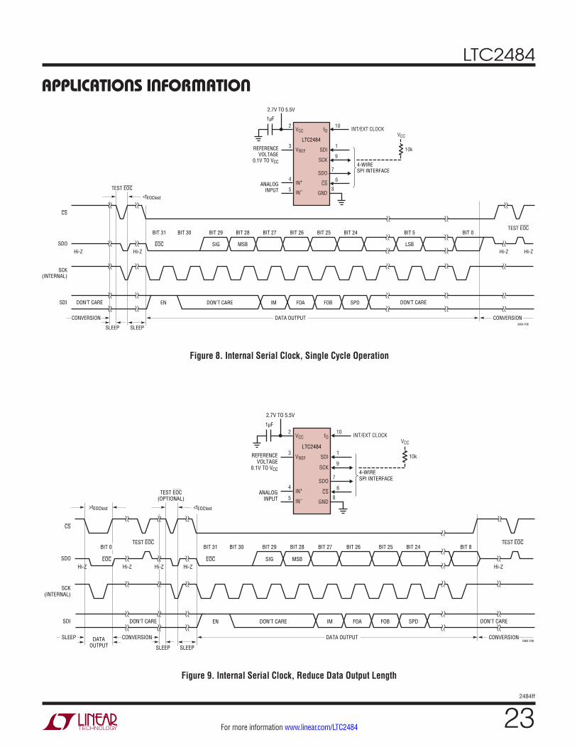
applicaTions inForMaTionInternal Serial Clock, Single Cycle Operation
This timing mode uses an internal serial clock to shift out the conversion result and a CS signal to monitor and control the state of the conversion cycle (see Figure 8).
In order to select the internal serial clock timing mode, the serial clock pin (SCK) must be floating (Hi-Z) or pulled HIGH prior to the falling edge of CS. The device will not enter the internal serial clock mode if SCK is driven LOW on the falling edge of CS. An internal weak pull-up resis-tor is active on the SCK pin during the falling edge of CS; therefore, the internal serial clock timing mode is automati-cally selected if SCK is not externally driven.
The serial data output pin (SDO) is Hi-Z as long as CS is HIGH. At any time during the conversion cycle, CS may be pulled LOW in order to monitor the state of the converter. Once CS is pulled LOW, SCK goes LOW and EOC is output to the SDO pin. EOC = 1 while a conversion is in progress and EOC = 0 if the device is in the sleep state.
When testing EOC, if the conversion is complete (EOC = 0), the device will exit the low power mode during the EOC test. In order to allow the device to return to the low power sleep state, CS must be pulled HIGH before the first rising edge of SCK. In the internal SCK timing mode, SCK goes HIGH and the device begins outputting data at time tEOCt-est after the falling edge of CS (if EOC = 0) or tEOCtest after EOC goes LOW (if CS is LOW during the falling edge of EOC). The value of tEOCtest is 12µs if the device is using its internal oscillator. If fO is driven by an external oscillator of frequency fEOSC, then tEOCtest is 3.6/fEOSC in seconds. If CS is pulled HIGH before time tEOCtest, the device returns to the sleep state and the conversion result is held in the internal static shift register.
If CS remains LOW longer than tEOCtest, the first rising edge of SCK will occur and the conversion result is serially shifted out of the SDO pin. The data I/O cycle concludes after the 32nd rising edge. The input data is shifted in via the SDI pin on the rising edge of SCK (including the first rising edge) and the output data is shifted out of the SDO pin on each falling edge of SCK. The internally generated serial clock is output to the SCK pin. This signal may be used to shift the conversion result into external circuitry. EOC can be latched on the first rising edge of SCK and
the last bit of the conversion result on the 32nd rising edge of SCK. After the 32nd rising edge, SDO goes HIGH (EOC = 1), SCK stays HIGH and a new conversion starts.
CS remains LOW during the data output state. However, the data output state may be aborted by pulling CS HIGH anytime between the first and 32nd rising edge of SCK (see Figure 9). On the rising edge of CS, the device aborts the data output state and immediately initiates a new conver-sion. If the device has not finished loading the last input bit (SPD) of SDI by the time CS is pulled HIGH, the SDI information is discarded and the previous configuration is still kept. This is useful for systems not requiring all 32 bits of output data, aborting an invalid conversion cycle, or synchronizing the start of a conversion. If CS is pulled HIGH while the converter is driving SCK LOW, the internal pull-up is not available to restore SCK to a logic HIGH state. This will cause the device to exit the internal serial clock mode on the next falling edge of CS. This can be avoided by adding an external 10k pull-up resistor to the SCK pin or by never pulling CS HIGH when SCK is LOW.
Whenever SCK is LOW, the LTC2484’s internal pull-up at pin SCK is disabled. Normally, SCK is not externally driven if the device is in the internal SCK timing mode. However, certain applications may require an external driver on SCK. If this driver goes Hi-Z after outputting a LOW signal, the LTC2484’s internal pull-up remains disabled. Hence, SCK remains LOW. On the next falling edge of CS, the device is switched to the external SCK timing mode. By adding an external 10k pull-up resistor to SCK, this pin goes HIGH once the external driver goes Hi-Z. On the next CS falling edge, the device will remain in the internal SCK timing mode.
A similar situation may occur during the sleep state when CS is pulsed HIGH-LOW-HIGH in order to test the conver-sion status. If the device is in the sleep state (EOC = 0), SCK will go LOW. Once CS goes HIGH (within the time period defined above as tEOCtest), the internal pull-up is activated. For a heavy capacitive load on the SCK pin, the internal pull-up may not be adequate to return SCK to a HIGH level before CS goes low again. This is not a concern under normal conditions where CS remains LOW after detecting EOC = 0. This situation is easily overcome by adding an external 10k pull-up resistor to the SCK pin.
LTC2484
232484ff
For more information www.linear.com/LTC2484
applicaTions inForMaTion
EN DON’T CARE IM FOA FOB SPDSDI DON’T CARE DON’T CARE
SDO
SCK(INTERNAL)
CS
>tEOCtest
MSBSIG
BIT 8
TEST EOC(OPTIONAL)
TEST EOCBIT 27 BIT 26 BIT 25 BIT 24BIT 28BIT 29BIT 30
EOC
BIT 31
EOC
BIT 0
SLEEPSLEEP
DATA OUTPUT
Hi-Z Hi-Z Hi-Z Hi-Z Hi-Z
DATAOUTPUT
CONVERSIONCONVERSIONSLEEP2484 F09
<tEOCtest
TEST EOC
VCC fO
VREF
IN+
IN–
SCK
SDI
SDO
CS
GND
2 10 INT/EXT CLOCK
3
4
5
910k
VCC
7
8
6
1REFERENCEVOLTAGE
0.1V TO VCC
ANALOGINPUT
1µF
2.7V TO 5.5V
LTC2484
4-WIRESPI INTERFACE
Figure 9. Internal Serial Clock, Reduce Data Output Length
EN DON’T CARE IM FOA FOB SPDSDI DON’T CARE DON’T CARE
SDO
SCK(INTERNAL)
CS
MSBSIG
BIT 0
LSB
BIT 5TEST EOC
BIT 27 BIT 26 BIT 25 BIT 24BIT 28BIT 29BIT 30
EOC
BIT 31
SLEEPSLEEP
DATA OUTPUT CONVERSIONCONVERSION2484 F08
<tEOCtest
Hi-Z Hi-Z Hi-Z Hi-Z
TEST EOC
VCC fO
VREF
IN+
IN–
SCK
SDI
SDO
CS
GND
2 10 INT/EXT CLOCK
3
4
5
910k
VCC
7
8
6
1REFERENCEVOLTAGE
0.1V TO VCC
ANALOGINPUT
1µF
2.7V TO 5.5V
LTC2484
4-WIRESPI INTERFACE
Figure 8. Internal Serial Clock, Single Cycle Operation
LTC2484
242484ff
For more information www.linear.com/LTC2484
applicaTions inForMaTionInternal Serial Clock, 3-Wire I/O, Continuous Conversion
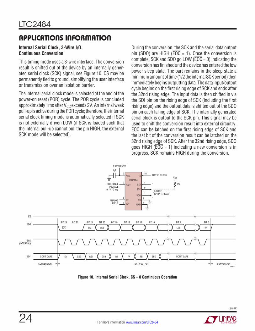
This timing mode uses a 3-wire interface. The conversion result is shifted out of the device by an internally gener-ated serial clock (SCK) signal, see Figure 10. CS may be permanently tied to ground, simplifying the user interface or transmission over an isolation barrier.
The internal serial clock mode is selected at the end of the power-on reset (POR) cycle. The POR cycle is concluded approximately 1ms after VCC exceeds 2V. An internal weak pull-up is active during the POR cycle; therefore, the internal serial clock timing mode is automatically selected if SCK is not externally driven LOW (if SCK is loaded such that the internal pull-up cannot pull the pin HIGH, the external SCK mode will be selected).
During the conversion, the SCK and the serial data output pin (SDO) are HIGH (EOC = 1). Once the conversion is complete, SCK and SDO go LOW (EOC = 0) indicating the conversion has finished and the device has entered the low power sleep state. The part remains in the sleep state a minimum amount of time (1/2 the internal SCK period) then immediately begins outputting data. The data input/output cycle begins on the first rising edge of SCK and ends after the 32nd rising edge. The input data is then shifted in via the SDI pin on the rising edge of SCK (including the first rising edge) and the output data is shifted out of the SDO pin on each falling edge of SCK. The internally generated serial clock is output to the SCK pin. This signal may be used to shift the conversion result into external circuitry. EOC can be latched on the first rising edge of SCK and the last bit of the conversion result can be latched on the 32nd rising edge of SCK. After the 32nd rising edge, SDO goes HIGH (EOC = 1) indicating a new conversion is in progress. SCK remains HIGH during the conversion.
EN GS2 GS1 GS0 IM FA FB SPDSDI* DON’T CARE DON’T CARE
SDO
SCK(INTERNAL)
CS
LSBMSBSIG
BIT 4 BIT 0
IM
BIT 19 BIT 18 BIT 17 BIT 16BIT 20BIT 21BIT 22
EOC
BIT 23
DATA OUTPUT CONVERSIONCONVERSION2484 F10
VCC fO
VREF
IN+
IN–
SCK
SDI
SDO
CS
GND
2 10 INT/EXT CLOCK
3
4
5
9
7
8
6
1REFERENCEVOLTAGE
0.1V TO VCC
ANALOGINPUT
1µF
2.7V TO 5.5V
LTC2484
3-WIRESPI INTERFACE
10k
VCC
Figure 10. Internal Serial Clock, CS = 0 Continuous Operation
LTC2484
252484ff
For more information www.linear.com/LTC2484
applicaTions inForMaTionPreserving the Converter Accuracy
The LTC2484 is designed to reduce as much as possible the conversion result sensitivity to device decoupling, PCB layout, anti-aliasing circuits, line frequency perturbations and so on. Nevertheless, in order to preserve the 24-bit accuracy capability of this part, some simple precautions are required.
Digital Signal Levels
The LTC2484’s digital interface is easy to use. Its digital inputs (SDI, fO, CS and SCK in External SCK mode of operation) accept standard CMOS logic levels and the internal hysteresis receivers can tolerate edge transition times as slow as 100µs. However, some considerations are required to take advantage of the exceptional accuracy and low supply current of this converter.
The digital output signals (SDO and SCK in Internal SCK mode of operation) are less of a concern because they are not generally active during the conversion state.
While a digital input signal is in the range 0.5V to (VCC – 0.5V), the CMOS input receiver draws additional current from the power supply. It should be noted that, when any one of the digital input signals (SDI, fO, CS and SCK in External SCK mode of operation) is within this range, the power supply current may increase even if the signal in question is at a valid logic level. For micropower operation, it is recommended to drive all digital input signals to full CMOS levels [VIL < 0.4V and VOH > (VCC – 0.4V)].
During the conversion period, the undershoot and/or overshoot of a fast digital signal connected to the pins can severely disturb the analog to digital conversion process. Undershoot and overshoot occur because of the imped-ance mismatch at the converter pin when the transition time of an external control signal is less than twice the propagation delay from the driver to the LTC2484. For reference, on a regular FR-4 board, signal propagation velocity is approximately 183ps/inch for internal traces and 170ps/inch for surface traces. Thus, a driver generating a control signal with a minimum transition time of 1ns must
be connected to the converter pin through a trace shorter than 2.5 inches. This problem becomes particularly difficult when shared control lines are used and multiple reflec-tions may occur. The solution is to carefully terminate all transmission lines close to their characteristic impedance.
Parallel termination near the LTC2484 pin will eliminate this problem but will increase the driver power dissipation. A series resistor between 27Ω and 56Ω placed near the driver output pin will also eliminate this problem without additional power dissipation. The actual resistor value de-pends upon the trace impedance and connection topology.
An alternate solution is to reduce the edge rate of the control signals. It should be noted that using very slow edges will increase the converter power supply current during the transition time. The differential input architecture reduces the converter’s sensitivity to ground currents.
Particular attention must be given to the connection of the fO signal when the LTC2484 is used with an external conversion clock. This clock is active during the conver-sion time and the normal mode rejection provided by the internal digital filter is not very high at this frequency. A normal mode signal of this frequency at the converter reference terminals can result in DC gain and INL errors. A normal mode signal of this frequency at the converter input terminals can result in a DC offset error. Such pertur-bations can occur due to asymmetric capacitive coupling between the fO signal trace and the converter input and/or reference connection traces. An immediate solution is to maintain maximum possible separation between the fO signal trace and the input/reference signals. When the fO signal is parallel terminated near the converter, substantial AC current is flowing in the loop formed by the fO con-nection trace, the termination and the ground return path. Thus, perturbation signals may be inductively coupled into the converter input and/or reference. In this situation, the user must reduce to a minimum the loop area for the fO signal as well as the loop area for the differential input and reference connections. Even when fO is not driven, other nearby signals pose similar EMI threats which will be minimized by following good layout practices.
LTC2484
262484ff
For more information www.linear.com/LTC2484
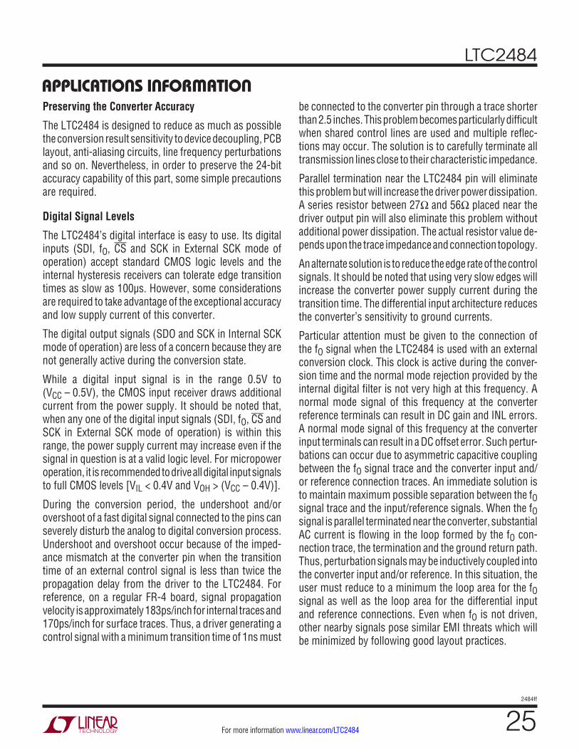
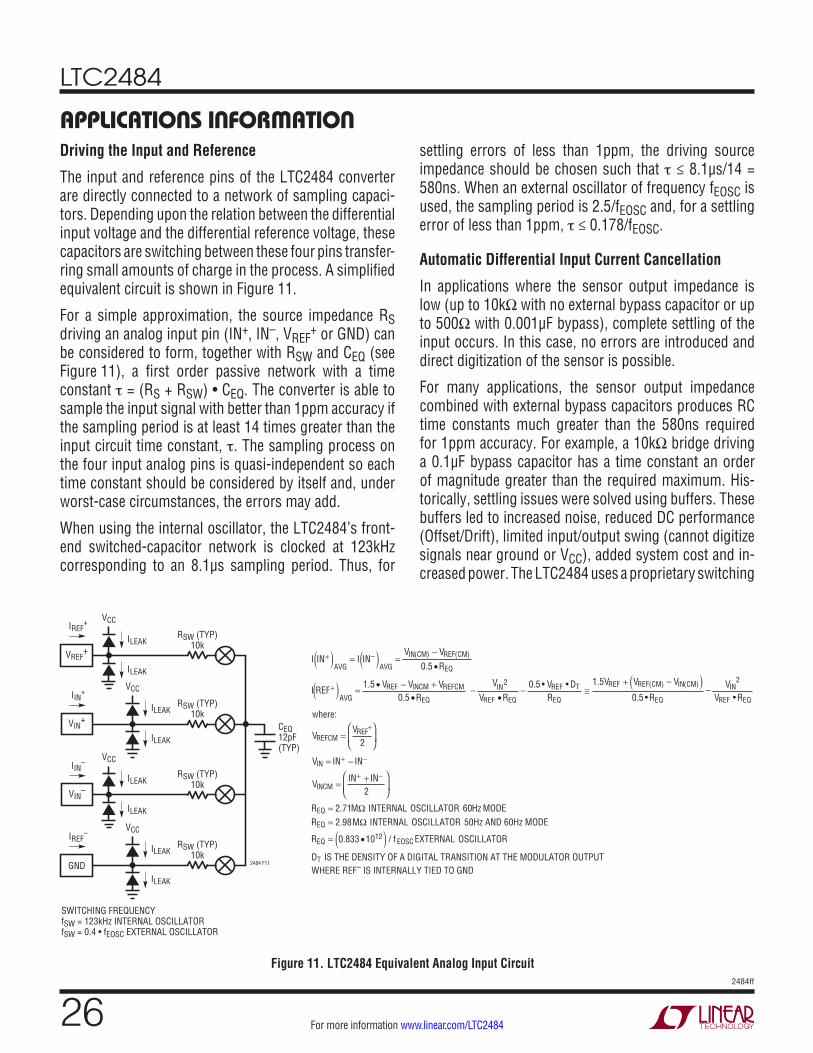
applicaTions inForMaTionDriving the Input and Reference
The input and reference pins of the LTC2484 converter are directly connected to a network of sampling capaci-tors. Depending upon the relation between the differential input voltage and the differential reference voltage, these capacitors are switching between these four pins transfer-ring small amounts of charge in the process. A simplified equivalent circuit is shown in Figure 11.
For a simple approximation, the source impedance RS driving an analog input pin (IN+, IN–, VREF
+ or GND) can be considered to form, together with RSW and CEQ (see Figure 11), a first order passive network with a time constant τ = (RS + RSW) • CEQ. The converter is able to sample the input signal with better than 1ppm accuracy if the sampling period is at least 14 times greater than the input circuit time constant, τ. The sampling process on the four input analog pins is quasi-independent so each time constant should be considered by itself and, under worst-case circumstances, the errors may add.
When using the internal oscillator, the LTC2484’s front-end switched-capacitor network is clocked at 123kHz corresponding to an 8.1µs sampling period. Thus, for
settling errors of less than 1ppm, the driving source impedance should be chosen such that τ ≤ 8.1µs/14 = 580ns. When an external oscillator of frequency fEOSC is used, the sampling period is 2.5/fEOSC and, for a settling error of less than 1ppm, τ ≤ 0.178/fEOSC.
Automatic Differential Input Current Cancellation
In applications where the sensor output impedance is low (up to 10kΩ with no external bypass capacitor or up to 500Ω with 0.001µF bypass), complete settling of the input occurs. In this case, no errors are introduced and direct digitization of the sensor is possible.
For many applications, the sensor output impedance combined with external bypass capacitors produces RC time constants much greater than the 580ns required for 1ppm accuracy. For example, a 10kΩ bridge driving a 0.1µF bypass capacitor has a time constant an order of magnitude greater than the required maximum. His-torically, settling issues were solved using buffers. These buffers led to increased noise, reduced DC performance (Offset/Drift), limited input/output swing (cannot digitize signals near ground or VCC), added system cost and in-creased power. The LTC2484 uses a proprietary switching
VREF+
VIN+
VCC
RSW (TYP)10k
ILEAK
ILEAK
VCC
ILEAK
ILEAK
VCC
RSW (TYP)10k
CEQ12pF(TYP)
RSW (TYP)10k
ILEAK
IIN+
VIN–
IIN–
IREF+
IREF–
2484 F11
ILEAK
VCC
ILEAK
ILEAK
SWITCHING FREQUENCYfSW = 123kHz INTERNAL OSCILLATORfSW = 0.4 • fEOSC EXTERNAL OSCILLATOR
GND
RSW (TYP)10k
Figure 11. LTC2484 Equivalent Analog Input Circuit
LTC2484
272484ff
For more information www.linear.com/LTC2484
applicaTions inForMaTionalgorithm that forces the average differential input current to zero independent of external settling errors. This allows accurate direct digitization of high impedance sensors without the need for buffers. Additional errors resulting from mismatched leakage currents must also be taken into account.
The switching algorithm forces the average input current on the positive input (IIN+) to be equal to the average input current on the negative input (IIN–). Over the complete conversion cycle, the average differential input current (IIN+ – IIN–) is zero. While the differential input current is zero, the common mode input current (IIN++ IIN–)/2 is proportional to the difference between the common mode input voltage (VINCM) and the common mode reference voltage (VREFCM).
In applications where the input common mode voltage is equal to the reference common mode voltage, as in the case of a balance bridge type application, both the differential and common mode input current are zero. The accuracy of the converter is unaffected by settling errors. Mismatches in source impedances between IN+ and IN– also do not affect the accuracy.
In applications where the input common mode voltage is constant but different from the reference common mode voltage, the differential input current remains zero while the common mode input current is proportional to the difference between VINCM and VREFCM. For a reference common mode of 2.5V and an input common mode of 1.5V, the common mode input current is approximately 0.74µA (in simultaneous 50Hz/60Hz rejection mode). This common mode input current has no effect on the accuracy if the external source impedances tied to IN+ and IN– are matched. Mismatches in these source impedances lead to a fixed offset error but do not affect the linearity or full-scale reading. A 1% mismatch in 1k source resistances leads to a 15ppm shift (74µV) in offset voltage.
In applications where the common mode input voltage varies as a function of input signal level (single-ended input, RTDs, half bridges, current sensors, etc.), the com-mon mode input current varies proportionally with input
voltage. For the case of balanced input impedances, the common mode input current effects are rejected by the large CMRR of the LTC2484 leading to little degradation in accuracy. Mismatches in source impedances lead to gain errors proportional to the difference between the common mode input voltage and the common mode reference voltage. 1% mismatches in 1k source resistances lead to gain worst-case gain errors on the order of 15ppm (for 1V differences in reference and input common mode voltage). Table 6 summarizes the effects of mismatched source impedance and differences in reference/input common mode voltages.
Table 6. Suggested Input Configuration for LTC2484 BALANCED INPUT RESISTANCES
UNBALANCED INPUT RESISTANCES
Constant VIN(CM) – VREF(CM)
CIN > 1nF at Both IN+ and IN–. Can Take Large Source Resistance with Negligible Error
CIN > 1nF at Both IN+ and IN–. Can Take Large Source Resistance. Unbalanced Resistance Results in an Offset Which Can Be Calibrated
Varying VIN(CM) – VREF(CM)
CIN > 1nF at Both IN+ and IN–. Can Take Large Source Resistance with Negligible Error
Minimize IN+ and IN– Capacitors and Avoid Large Source Impedance (<5k Recommended)
The magnitude of the dynamic input current depends upon the size of the very stable internal sampling capacitors and upon the accuracy of the converter sampling clock. The accuracy of the internal clock over the entire temperature and power supply range is typically better than 0.5%. Such a specification can also be easily achieved by an external clock. When relatively stable resistors (50ppm/°C) are used for the external source impedance seen by IN+ and IN–, the expected drift of the dynamic current and offset will be insignificant (about 1% of their respective values over the entire temperature and voltage range). Even for the most stringent applications, a one-time calibration operation may be sufficient.
In addition to the input sampling charge, the input ESD protection diodes have a temperature dependent leakage current. This current, nominally 1nA (±10nA max), results in a small offset shift. A 1k source resistance will create a 1µV typical and 10µV maximum offset voltage.
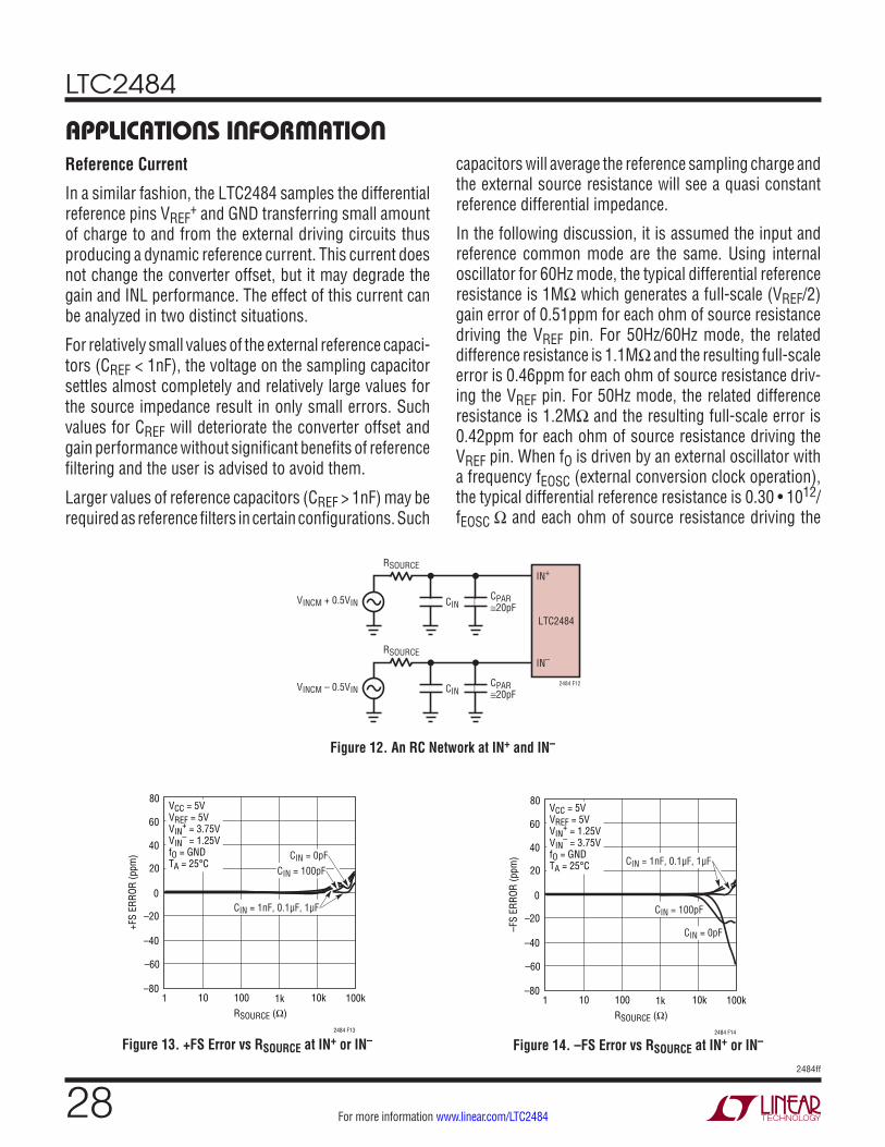
LTC2484
282484ff
For more information www.linear.com/LTC2484
Reference Current
In a similar fashion, the LTC2484 samples the differential reference pins VREF
+ and GND transferring small amount of charge to and from the external driving circuits thus producing a dynamic reference current. This current does not change the converter offset, but it may degrade the gain and INL performance. The effect of this current can be analyzed in two distinct situations.
For relatively small values of the external reference capaci-tors (CREF < 1nF), the voltage on the sampling capacitor settles almost completely and relatively large values for the source impedance result in only small errors. Such values for CREF will deteriorate the converter offset and gain performance without significant benefits of reference filtering and the user is advised to avoid them.
Larger values of reference capacitors (CREF > 1nF) may be required as reference filters in certain configurations. Such
capacitors will average the reference sampling charge and the external source resistance will see a quasi constant reference differential impedance.
In the following discussion, it is assumed the input and reference common mode are the same. Using internal oscillator for 60Hz mode, the typical differential reference resistance is 1MΩ which generates a full-scale (VREF/2) gain error of 0.51ppm for each ohm of source resistance driving the VREF pin. For 50Hz/60Hz mode, the related difference resistance is 1.1MΩ and the resulting full-scale error is 0.46ppm for each ohm of source resistance driv-ing the VREF pin. For 50Hz mode, the related difference resistance is 1.2MΩ and the resulting full-scale error is 0.42ppm for each ohm of source resistance driving the VREF pin. When fO is driven by an external oscillator with a frequency fEOSC (external conversion clock operation), the typical differential reference resistance is 0.30 • 1012/fEOSC Ω and each ohm of source resistance driving the
CIN
2484 F12
VINCM + 0.5VIN
RSOURCEIN+
LTC2484
CPAR≅20pF
CINVINCM – 0.5VIN
RSOURCEIN–
CPAR≅20pF
Figure 12. An RC Network at IN+ and IN–
RSOURCE (Ω)1
+FS
ERRO
R (p
pm)
–20
0
20
1k 100k
2484 F13
–40
–60
–8010 100 10k
40
60
80VCC = 5VVREF = 5VVIN
+ = 3.75VVIN
– = 1.25VfO = GNDTA = 25°C
CIN = 0pFCIN = 100pF
CIN = 1nF, 0.1µF, 1µF
Figure 13. +FS Error vs RSOURCE at IN+ or IN–
RSOURCE (Ω)1
–FS
ERRO
R (p
pm)
–20
0
20
1k 100k
2484 F14
–40
–60
–8010 100 10k
40
60
80VCC = 5VVREF = 5VVIN
+ = 1.25VVIN
– = 3.75VfO = GNDTA = 25°C
CIN = 0pF
CIN = 100pF
CIN = 1nF, 0.1µF, 1µF
Figure 14. –FS Error vs RSOURCE at IN+ or IN–
applicaTions inForMaTion
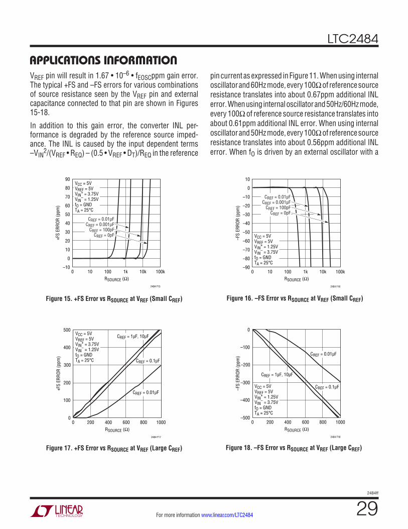
LTC2484
292484ff
For more information www.linear.com/LTC2484
VREF pin will result in 1.67 • 10–6 • fEOSCppm gain error. The typical +FS and –FS errors for various combinations of source resistance seen by the VREF pin and external capacitance connected to that pin are shown in Figures 15-18.
In addition to this gain error, the converter INL per-formance is degraded by the reference source imped-ance. The INL is caused by the input dependent terms –VIN
2/(VREF • REQ) – (0.5 • VREF • DT)/REQ in the reference
pin current as expressed in Figure 11. When using internal oscillator and 60Hz mode, every 100Ω of reference source resistance translates into about 0.67ppm additional INL error. When using internal oscillator and 50Hz/60Hz mode, every 100Ω of reference source resistance translates into about 0.61ppm additional INL error. When using internal oscillator and 50Hz mode, every 100Ω of reference source resistance translates into about 0.56ppm additional INL error. When fO is driven by an external oscillator with a
RSOURCE (Ω)0
+FS
ERRO
R (p
pm)
50
70
90
10k
2484 F15
30
10
40
60
80
20
0
–1010 100 1k 100k
VCC = 5VVREF = 5VVIN
+ = 3.75VVIN
– = 1.25VfO = GNDTA = 25°C
CREF = 0.01µFCREF = 0.001µF
CREF = 100pFCREF = 0pF
Figure 15. +FS Error vs RSOURCE at VREF (Small CREF)
RSOURCE (Ω)0
–FS
ERRO
R (p
pm)
–30
–10
10
10k
2484 F16
–50
–70
–40
–20
0
–60
–80
–9010 100 1k 100k
VCC = 5VVREF = 5VVIN
+ = 1.25VVIN
– = 3.75VfO = GNDTA = 25°C
CREF = 0.01µFCREF = 0.001µF
CREF = 100pFCREF = 0pF
Figure 16. –FS Error vs RSOURCE at VREF (Small CREF)
RSOURCE (Ω)0
+FS
ERRO
R (p
pm)
300
400
500
800
2484 F17
200
100
0200 400 600 1000
VCC = 5VVREF = 5VVIN
+ = 3.75VVIN
– = 1.25VfO = GNDTA = 25°C
CREF = 1µF, 10µF
CREF = 0.1µF
CREF = 0.01µF
Figure 17. +FS Error vs RSOURCE at VREF (Large CREF) Figure 18. –FS Error vs RSOURCE at VREF (Large CREF)
RSOURCE (Ω)0
–FS
ERRO
R (p
pm)
–200
–100
0
800
2484 F18
–300
–400
–500200 400 600 1000
VCC = 5VVREF = 5VVIN
+ = 1.25VVIN
– = 3.75VfO = GNDTA = 25°C
CREF = 1µF, 10µF
CREF = 0.1µF
CREF = 0.01µF
applicaTions inForMaTion
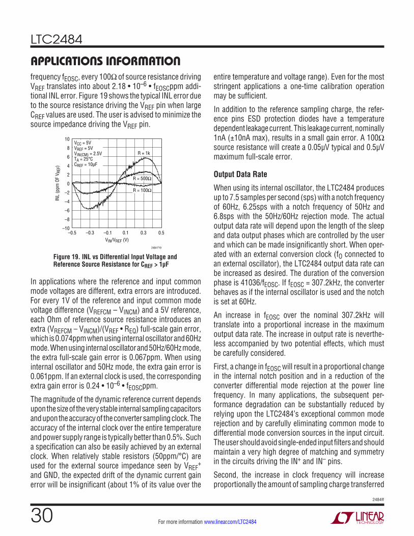
LTC2484
302484ff
For more information www.linear.com/LTC2484
frequency fEOSC, every 100Ω of source resistance driving VREF translates into about 2.18 • 10–6 • fEOSCppm addi-tional INL error. Figure 19 shows the typical INL error due to the source resistance driving the VREF pin when large CREF values are used. The user is advised to minimize the source impedance driving the VREF pin.
entire temperature and voltage range). Even for the most stringent applications a one-time calibration operation may be sufficient.
In addition to the reference sampling charge, the refer-ence pins ESD protection diodes have a temperature dependent leakage current. This leakage current, nominally 1nA (±10nA max), results in a small gain error. A 100Ω source resistance will create a 0.05µV typical and 0.5µV maximum full-scale error.
Output Data Rate
When using its internal oscillator, the LTC2484 produces up to 7.5 samples per second (sps) with a notch frequency of 60Hz, 6.25sps with a notch frequency of 50Hz and 6.8sps with the 50Hz/60Hz rejection mode. The actual output data rate will depend upon the length of the sleep and data output phases which are controlled by the user and which can be made insignificantly short. When oper-ated with an external conversion clock (fO connected to an external oscillator), the LTC2484 output data rate can be increased as desired. The duration of the conversion phase is 41036/fEOSC. If fEOSC = 307.2kHz, the converter behaves as if the internal oscillator is used and the notch is set at 60Hz.
An increase in fEOSC over the nominal 307.2kHz will translate into a proportional increase in the maximum output data rate. The increase in output rate is neverthe-less accompanied by two potential effects, which must be carefully considered.
First, a change in fEOSC will result in a proportional change in the internal notch position and in a reduction of the converter differential mode rejection at the power line frequency. In many applications, the subsequent per-formance degradation can be substantially reduced by relying upon the LTC2484’s exceptional common mode rejection and by carefully eliminating common mode to differential mode conversion sources in the input circuit. The user should avoid single-ended input filters and should maintain a very high degree of matching and symmetry in the circuits driving the IN+ and IN– pins.
Second, the increase in clock frequency will increase proportionally the amount of sampling charge transferred
Figure 19. INL vs Differential Input Voltage and Reference Source Resistance for CREF > 1µF
VIN/VREF (V)–0.5
INL
(ppm
OF
V REF
)
2
6
10
0.3
2484 F19
–2
–6
0
4
8
–4
–8
–10–0.3 –0.1 0.1 0.5
VCC = 5VVREF = 5VVIN(CM) = 2.5VTA = 25°CCREF = 10µF
R = 1k
R = 100Ω
R = 500Ω
In applications where the reference and input common mode voltages are different, extra errors are introduced. For every 1V of the reference and input common mode voltage difference (VREFCM – VINCM) and a 5V reference, each Ohm of reference source resistance introduces an extra (VREFCM – VINCM)/(VREF • REQ) full-scale gain error, which is 0.074ppm when using internal oscillator and 60Hz mode. When using internal oscillator and 50Hz/60Hz mode, the extra full-scale gain error is 0.067ppm. When using internal oscillator and 50Hz mode, the extra gain error is 0.061ppm. If an external clock is used, the corresponding extra gain error is 0.24 • 10–6 • fEOSCppm.
The magnitude of the dynamic reference current depends upon the size of the very stable internal sampling capacitors and upon the accuracy of the converter sampling clock. The accuracy of the internal clock over the entire temperature and power supply range is typically better than 0.5%. Such a specification can also be easily achieved by an external clock. When relatively stable resistors (50ppm/°C) are used for the external source impedance seen by VREF
+ and GND, the expected drift of the dynamic current gain error will be insignificant (about 1% of its value over the
applicaTions inForMaTion
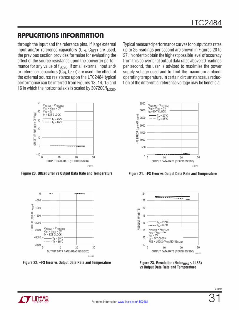
LTC2484
312484ff
For more information www.linear.com/LTC2484
through the input and the reference pins. If large external input and/or reference capacitors (CIN, CREF) are used, the previous section provides formulae for evaluating the effect of the source resistance upon the converter perfor-mance for any value of fEOSC. If small external input and/or reference capacitors (CIN, CREF) are used, the effect of the external source resistance upon the LTC2484 typical performance can be inferred from Figures 13, 14, 15 and 16 in which the horizontal axis is scaled by 307200/fEOSC.
Typical measured performance curves for output data rates up to 25 readings per second are shown in Figures 20 to 27. In order to obtain the highest possible level of accuracy from this converter at output data rates above 20 readings per second, the user is advised to maximize the power supply voltage used and to limit the maximum ambient operating temperature. In certain circumstances, a reduc-tion of the differential reference voltage may be beneficial.
OUTPUT DATA RATE (READINGS/SEC)
–10
OFFS
ET E
RROR
(ppm
OF
V REF
)
10
30
50
0
20
40
20
2484 F20
100 30
VIN(CM) = VREF(CM)VCC = VREF = 5VVIN = 0VfO = EXT CLOCK
TA = 25°CTA = 85°C
Figure 20. Offset Error vs Output Data Rate and Temperature
OUTPUT DATA RATE (READINGS/SEC)0
0
+FS
ERRO
R (p
pm O
F V R
EF)
500
1500
2000
2500
3500
10
2484 F21
1000
3000
20 30
VIN(CM) = VREF(CM)VCC = VREF = 5VfO = EXT CLOCK
TA = 25°CTA = 85°C
Figure 21. +FS Error vs Output Data Rate and Temperature
Figure 22. –FS Error vs Output Data Rate and Temperature
OUTPUT DATA RATE (READINGS/SEC)0
–3500
–FS
ERRO
R (p
pm O
F V R
EF)
–3000
–2000
–1500
–1000
0
10
2484 F22
–2500
–500
20 30
VIN(CM) = VREF(CM)VCC = VREF = 5VfO = EXT CLOCK
TA = 25°CTA = 85°C
OUTPUT DATA RATE (READINGS/SEC)0
10
RESO
LUTI
ON (B
ITS)
12
16
18
20
24
10
2484 F23
14
22
3020
VIN(CM) = VREF(CM)VCC = VREF = 5VVIN = 0VfO = EXT CLOCKRES = LOG 2 (VREF/NOISERMS)
TA = 25°CTA = 85°C
Figure 23. Resolution (NoiseRMS ≤ 1LSB) vs Output Data Rate and Temperature
applicaTions inForMaTion
LTC2484
322484ff
For more information www.linear.com/LTC2484
Input Bandwidth
The combined effect of the internal SINC4 digital filter and of the analog and digital auto-calibration circuits determines the LTC2484 input bandwidth. When the internal oscillator is used with the notch set at 60Hz, the 3dB input bandwidth is 3.63Hz. When the internal oscillator is used with the notch set at 50Hz, the 3dB input bandwidth is 3.02Hz. If an external conversion clock generator of frequency fEOSC is connected to the fO pin, the 3dB input bandwidth is 11.8 • 10–6 • fEOSC.
OUTPUT DATA RATE (READINGS/SEC)0
10
RESO
LUTI
ON (B
ITS)
12
16
18
22
10
2484 F24
14
20
3020
VIN(CM) = VREF(CM)VCC = VREF = 5VfO = EXT CLOCKRES = LOG 2 (VREF/INLMAX)
TA = 25°CTA = 85°C
Figure 24. Resolution (INLMAX ≤ 1LSB) vs Output Data Rate and Temperature
OUTPUT DATA RATE (READINGS/SEC)0
–10
OFFS
ET E
RROR
(ppm
OF
V REF
)
–5
5
10
20
10
2484 F25
0
15
3020
VIN(CM) = VREF(CM)VIN = 0VfO = EXT CLOCKTA = 25°C
VCC = 5V, VREF = 2.5VVCC = VREF = 5V
Figure 25. Offset Error vs Output Data Rate and Reference Voltage
Figure 26. Resolution (NoiseRMS ≤ 1LSB) vs Output Data Rate and Reference Voltage
Figure 27. Resolution (INLMAX ≤ 1LSB) vs Output Data Rate and Reference Voltage
OUTPUT DATA RATE (READINGS/SEC)0
10
RESO
LUTI
ON (B
ITS)
12
16
18
20
24
10
2484 F26
14
22
3020
VIN(CM) = VREF(CM)VIN = 0VfO = EXT CLOCKTA = 25°CRES = LOG 2 (VREF/NOISERMS)
VCC = 5V, VREF = 2.5VVCC = VREF = 5V
OUTPUT DATA RATE (READINGS/SEC)0
10
RESO
LUTI
ON (B
ITS)
12
16
18
22
10
2484 F27
14
20
3020
VIN(CM) = VREF(CM)VIN = 0VREF– = GNDfO = EXT CLOCKTA = 25°CRES = LOG 2 (VREF/INLMAX)
VCC = 5V, VREF = 2.5VVCC = VREF = 5V
Due to the complex filtering and calibration algorithms utilized, the converter input bandwidth is not modeled very accurately by a first order filter with the pole located at the 3dB frequency. When the internal oscillator is used, the shape of the LTC2484 input bandwidth is shown in Figure 28. When an external oscillator of frequency fEOSC is used, the shape of the LTC2484 input bandwidth can be derived from Figure 28, 60Hz mode curve in which the horizontal axis is scaled by fEOSC/307200.
applicaTions inForMaTion
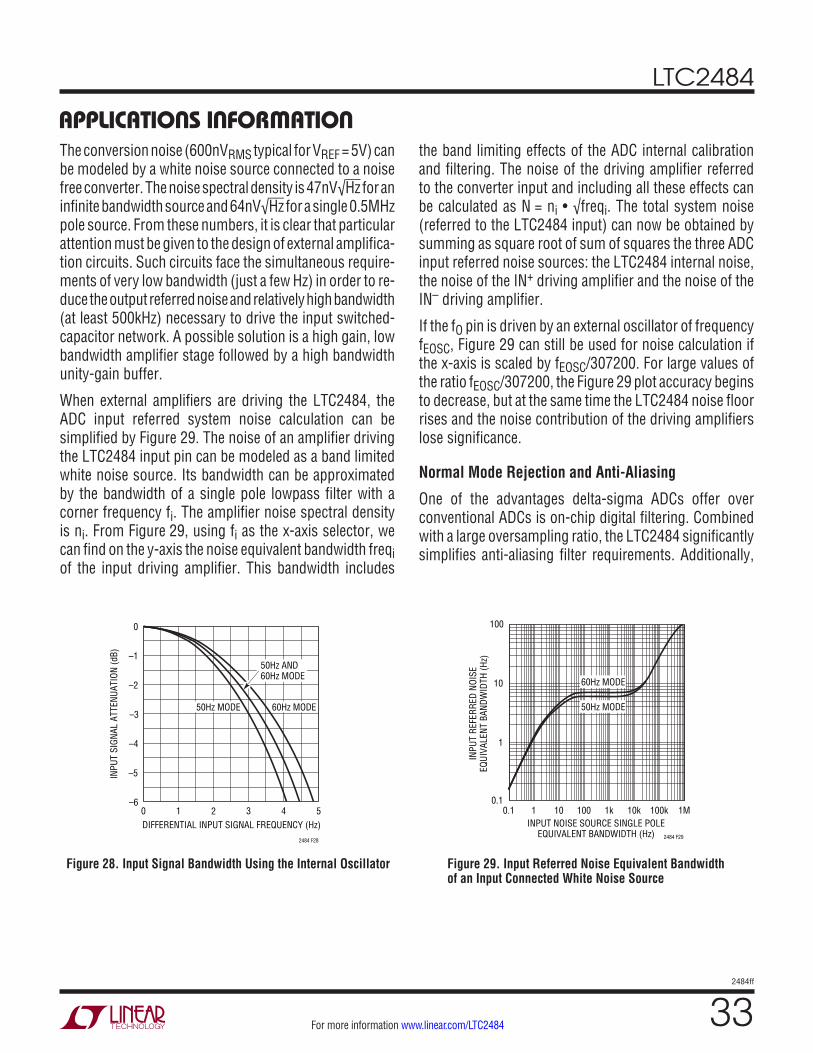
LTC2484
332484ff
For more information www.linear.com/LTC2484
The conversion noise (600nVRMS typical for VREF = 5V) can be modeled by a white noise source connected to a noise free converter. The noise spectral density is 47nV√Hz for an infinite bandwidth source and 64nV√Hz for a single 0.5MHz pole source. From these numbers, it is clear that particular attention must be given to the design of external amplifica-tion circuits. Such circuits face the simultaneous require-ments of very low bandwidth (just a few Hz) in order to re-duce the output referred noise and relatively high bandwidth (at least 500kHz) necessary to drive the input switched- capacitor network. A possible solution is a high gain, low bandwidth amplifier stage followed by a high bandwidth unity-gain buffer.
When external amplifiers are driving the LTC2484, the ADC input referred system noise calculation can be simplified by Figure 29. The noise of an amplifier driving the LTC2484 input pin can be modeled as a band limited white noise source. Its bandwidth can be approximated by the bandwidth of a single pole lowpass filter with a corner frequency fi. The amplifier noise spectral density is ni. From Figure 29, using fi as the x-axis selector, we can find on the y-axis the noise equivalent bandwidth freqi of the input driving amplifier. This bandwidth includes
the band limiting effects of the ADC internal calibration and filtering. The noise of the driving amplifier referred to the converter input and including all these effects can be calculated as N = ni • √freqi. The total system noise (referred to the LTC2484 input) can now be obtained by summing as square root of sum of squares the three ADC input referred noise sources: the LTC2484 internal noise, the noise of the IN+ driving amplifier and the noise of the IN– driving amplifier.
If the fO pin is driven by an external oscillator of frequency fEOSC, Figure 29 can still be used for noise calculation if the x-axis is scaled by fEOSC/307200. For large values of the ratio fEOSC/307200, the Figure 29 plot accuracy begins to decrease, but at the same time the LTC2484 noise floor rises and the noise contribution of the driving amplifiers lose significance.
Normal Mode Rejection and Anti-Aliasing
One of the advantages delta-sigma ADCs offer over conventional ADCs is on-chip digital filtering. Combined with a large oversampling ratio, the LTC2484 significantly simplifies anti-aliasing filter requirements. Additionally,
DIFFERENTIAL INPUT SIGNAL FREQUENCY (Hz)0
INPU
T SI
GNAL
ATT
ENUA
TION
(dB)
–3
–2
–1
0
4
2484 F28
–4
–5
–61 2 3 5
50Hz MODE 60Hz MODE
50Hz AND 60Hz MODE
Figure 28. Input Signal Bandwidth Using the Internal Oscillator
INPUT NOISE SOURCE SINGLE POLEEQUIVALENT BANDWIDTH (Hz)
1
INPU
T RE
FERR
ED N
OISE
EQUI
VALE
NT B
ANDW
IDTH
(Hz)
10
0.1 1 10 100 1k 10k 100k 1M
2484 F29
0.1
100
50Hz MODE
60Hz MODE
Figure 29. Input Referred Noise Equivalent Bandwidth of an Input Connected White Noise Source
applicaTions inForMaTion
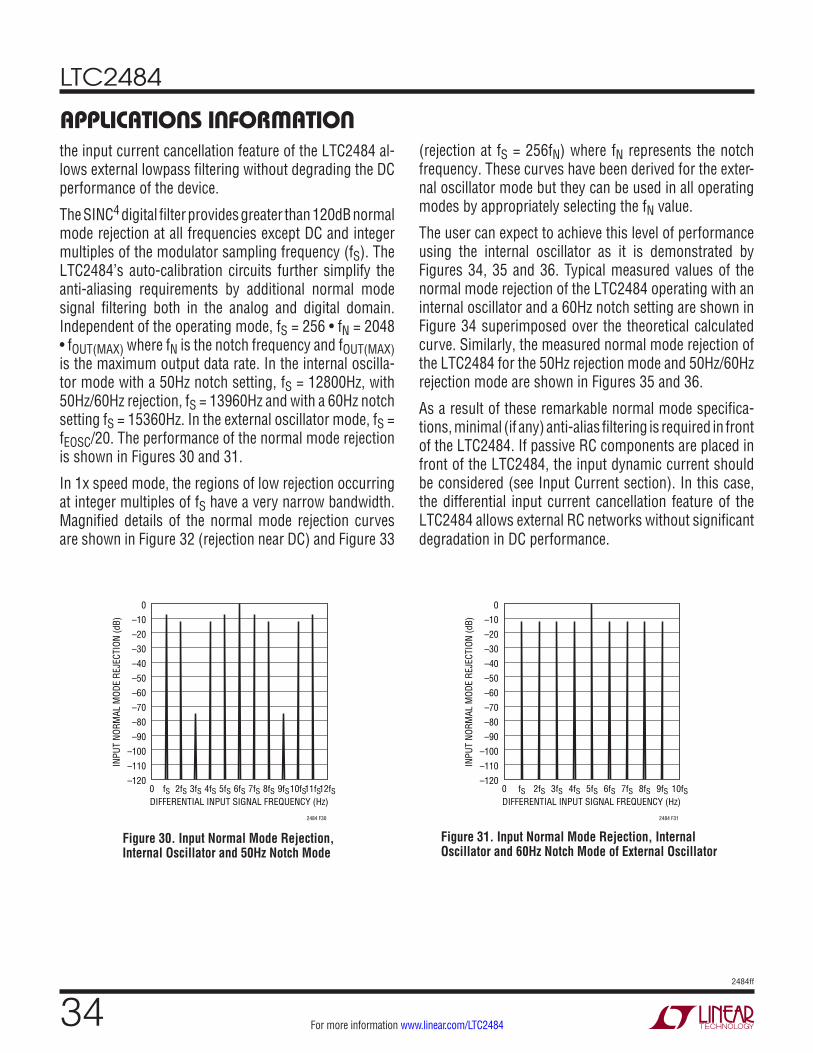
LTC2484
342484ff
For more information www.linear.com/LTC2484
the input current cancellation feature of the LTC2484 al-lows external lowpass filtering without degrading the DC performance of the device.
The SINC4 digital filter provides greater than 120dB normal mode rejection at all frequencies except DC and integer multiples of the modulator sampling frequency (fS). The LTC2484’s auto-calibration circuits further simplify the anti-aliasing requirements by additional normal mode signal filtering both in the analog and digital domain. Independent of the operating mode, fS = 256 • fN = 2048 • fOUT(MAX) where fN is the notch frequency and fOUT(MAX) is the maximum output data rate. In the internal oscilla-tor mode with a 50Hz notch setting, fS = 12800Hz, with 50Hz/60Hz rejection, fS = 13960Hz and with a 60Hz notch setting fS = 15360Hz. In the external oscillator mode, fS = fEOSC/20. The performance of the normal mode rejection is shown in Figures 30 and 31.
In 1x speed mode, the regions of low rejection occurring at integer multiples of fS have a very narrow bandwidth. Magnified details of the normal mode rejection curves are shown in Figure 32 (rejection near DC) and Figure 33
(rejection at fS = 256fN) where fN represents the notch frequency. These curves have been derived for the exter-nal oscillator mode but they can be used in all operating modes by appropriately selecting the fN value.
The user can expect to achieve this level of performance using the internal oscillator as it is demonstrated by Figures 34, 35 and 36. Typical measured values of the normal mode rejection of the LTC2484 operating with an internal oscillator and a 60Hz notch setting are shown in Figure 34 superimposed over the theoretical calculated curve. Similarly, the measured normal mode rejection of the LTC2484 for the 50Hz rejection mode and 50Hz/60Hz rejection mode are shown in Figures 35 and 36.
As a result of these remarkable normal mode specifica-tions, minimal (if any) anti-alias filtering is required in front of the LTC2484. If passive RC components are placed in front of the LTC2484, the input dynamic current should be considered (see Input Current section). In this case, the differential input current cancellation feature of the LTC2484 allows external RC networks without significant degradation in DC performance.
DIFFERENTIAL INPUT SIGNAL FREQUENCY (Hz)0 fS 2fS 3fS 4fS 5fS 6fS 7fS 8fS 9fS10fS11fS12fS
INPU
T NO
RMAL
MOD
E RE
JECT
ION
(dB)
2484 F30
0
–10
–20
–30
–40
–50
–60
–70
–80
–90
–100
–110
–120
DIFFERENTIAL INPUT SIGNAL FREQUENCY (Hz)0 fS
INPU
T NO
RMAL
MOD
E RE
JECT
ION
(dB)
2484 F31
0
–10
–20
–30
–40
–50
–60
–70
–80
–90
–100
–110
–1202fS 3fS 4fS 5fS 6fS 7fS 8fS 9fS 10fS
Figure 30. Input Normal Mode Rejection, Internal Oscillator and 50Hz Notch Mode
Figure 31. Input Normal Mode Rejection, Internal Oscillator and 60Hz Notch Mode of External Oscillator
applicaTions inForMaTion
LTC2484
352484ff
For more information www.linear.com/LTC2484
INPUT SIGNAL FREQUENCY (Hz)
INPU
T NO
RMAL
MOD
E RE
JECT
ION
(dB)
2484 F32
0
–10
–20
–30
–40
–50
–60
–70
–80
–90
–100
–110
–120fN0 2fN 3fN 4fN 5fN 6fN 7fN 8fN
INPUT SIGNAL FREQUENCY (Hz)250fN 252fN 254fN 256fN 258fN 260fN 262fN
INPU
T NO
RMAL
MOD
E RE
JECT
ION
(dB)
2484 F33
0
–10
–20
–30
–40
–50
–60
–70
–80
–90
–100
–110
–120
Figure 32. Input Normal Mode Rejection at DC Figure 33. Input Normal Mode Rejection at fS = 256fN
INPUT FREQUENCY (Hz)0 15 30 45 60 75 90 105 120 135 150 165 180 195 210 225 240
NORM
AL M
ODE
REJE
CTIO
N (d
B)
2484 F34
0
–20
–40
–60
–80
–100
–120
VCC = 5VVREF = 5VVIN(CM) = 2.5VVIN(P-P) = 5VTA = 25°C
MEASURED DATACALCULATED DATA
Figure 34. Input Normal Mode Rejection vs Input Frequency with Input Perturbation of 100% Full-Scale (60Hz Notch)
INPUT FREQUENCY (Hz)0 12.5 25 37.5 50 62.5 75 87.5 100 112.5 125 137.5 150 162.5 175 187.5 200
NORM
AL M
ODE
REJE
CTIO
N (d
B)
2484 F35
0
–20
–40
–60
–80
–100
–120
VCC = 5VVREF = 5VVIN(CM) = 2.5VVIN(P-P) = 5VTA = 25°C
MEASURED DATACALCULATED DATA
Figure 35. Input Normal Mode Rejection vs Input Frequency with Input Perturbation of 100% Full-Scale (50Hz Notch)
Figure 36. Input Normal Mode Rejection vs Input Frequency with Input Perturbation of 100% Full-Scale (50Hz/60Hz Mode)
INPUT FREQUENCY (Hz)0 20 40 60 80 100 120 140 160 180 200 220
NORM
AL M
ODE
REJE
CTIO
N (d
B)
2484 F36
0
–20
–40
–60
–80
–100
–120
VCC = 5VVREF = 5VVIN(CM) = 2.5VVIN(P-P) = 5VTA = 25°C
MEASURED DATACALCULATED DATA
applicaTions inForMaTion
LTC2484
362484ff
For more information www.linear.com/LTC2484
Traditional high order delta-sigma modulators, while pro-viding very good linearity and resolution, suffer from poten-tial instabilities at large input signal levels. The proprietary architecture used for the LTC2484 third order modulator resolves this problem and guarantees a predictable stable behavior at input signal levels of up to 150% of full-scale. In many industrial applications, it is not uncommon to have to measure microvolt level signals superimposed over volt level perturbations and the LTC2484 is eminently suited for such tasks. When the perturbation is differential, the specification of interest is the normal mode rejection for large input signal levels. With a reference voltage VREF = 5V, the LTC2484 has a full-scale differential input range of 5V peak-to-peak. Figures 37 and 38 show measurement results for the LTC2484 normal mode rejection ratio with a 7.5V peak-to-peak (150% of full-scale) input signal
superimposed over the more traditional normal mode rejection ratio results obtained with a 5V peak-to-peak (full-scale) input signal. In Figure 37, the LTC2484 uses the internal oscillator with the notch set at 60Hz (fO = LOW) and in Figure 38 it uses the internal oscillator with the notch set at 50Hz. It is clear that the LTC2484 rejec-tion performance is maintained with no compromises in this extreme situation. When operating with large input signal levels, the user must observe that such signals do not violate the device absolute maximum ratings.
Using the 2x speed mode of the LTC2484, the device bypasses the digital offset calibration operation to double the output data rate. The superior normal mode rejection is maintained as shown in Figures 30 and 31. However, the magnified details near DC and fS = 256fN are different,
INPUT FREQUENCY (Hz)0 15 30 45 60 75 90 105 120 135 150 165 180 195 210 225 240
NORM
AL M
ODE
REJE
CTIO
N (d
B)
2484 F37
0
–20
–40
–60
–80
–100
–120
VCC = 5VVREF = 5VVINCM = 2.5VTA = 25°C
VIN(P-P) = 5VVIN(P-P) = 7.5V(150% OF FULL SCALE)
INPUT FREQUENCY (Hz)0
NORM
AL M
ODE
REJE
CTIO
N (d
B)
2484 F38
0
–20
–40
–60
–80
–100
–120
VCC = 5VVREF = 5VVIN(CM) = 2.5VTA = 25°C
VIN(P-P) = 5VVIN(P-P) = 7.5V(150% OF FULL SCALE)
12.5 25 37.5 50 62.5 75 87.5 100 112.5 125 137.5 150 162.5 175 187.5 200
Figure 37. Measured Input Normal Mode Rejection vs Input Freq-uency with Input Perturbation of 150% Full-Scale (60Hz Notch)
Figure 38. Measured Input Normal Mode Rejection vs Input Freq-uency with Input Perturbation of 150% Full-Scale (50Hz Notch)
applicaTions inForMaTion
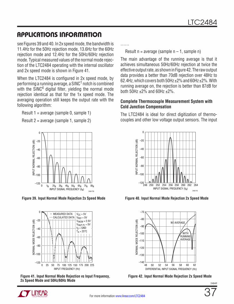
LTC2484
372484ff
For more information www.linear.com/LTC2484
INPUT SIGNAL FREQUENCY (fN)
INPU
T NO
RMAL
REJ
ECTI
ON (d
B)
2484 F39
0
–20
–40
–60
–80
–100
–1200 fN 2fN 3fN 4fN 5fN 6fN 7fN 8fN
INPUT SIGNAL FREQUENCY (fN)
INPU
T NO
RMAL
REJ
ECTI
ON (d
B)
2484 F40
0
–20
–40
–60
–80
–100
–120250248 252 254 256 258 260 262 264
Figure 39. Input Normal Mode Rejection 2x Speed Mode Figure 40. Input Normal Mode Rejection 2x Speed Mode
INPUT FREQUENCY (Hz)0
NORM
AL M
ODE
REJE
CTIO
N (d
B)
50 100 125 225
2484 F41
25 75 150 175 200
0
–20
–40
–60
–80
–100
–120
VCC = 5VVREF = 5VVINCM = 2.5VVIN(P-P) = 5VfO = GNDTA = 25°C
MEASURED DATACALCULATED DATA
Figure 41. Input Normal Mode Rejection vs Input Frequency, 2x Speed Mode and 50Hz/60Hz Mode
DIFFERENTIAL INPUT SIGNAL FREQUENCY (Hz)48
–70
–80
–90
–100
–110
–120
–130
–14054 58
2484 F42
50 52 56 60 62
NORM
AL M
ODE
REJE
CTIO
N (d
B)
NO AVERAGE
WITHRUNNINGAVERAGE
Figure 42. Input Normal Mode Rejection 2x Speed Mode
see Figures 39 and 40. In 2x speed mode, the bandwidth is 11.4Hz for the 50Hz rejection mode, 13.6Hz for the 60Hz rejection mode and 12.4Hz for the 50Hz/60Hz rejection mode. Typical measured values of the normal mode rejec-tion of the LTC2484 operating with the internal oscillator and 2x speed mode is shown in Figure 41.
When the LTC2484 is configured in 2x speed mode, by performing a running average, a SINC1 notch is combined with the SINC4 digital filter, yielding the normal mode rejection identical as that for the 1x speed mode. The averaging operation still keeps the output rate with the following algorithm:
Result 1 = average (sample 0, sample 1)
Result 2 = average (sample 1, sample 2)
……
Result n = average (sample n – 1, sample n)
The main advantage of the running average is that it achieves simultaneous 50Hz/60Hz rejection at twice the effective output rate, as shown in Figure 42. The raw output data provides a better than 70dB rejection over 48Hz to 62.4Hz, which covers both 50Hz ±2% and 60Hz ±2%. With running average on, the rejection is better than 87dB for both 50Hz ±2% and 60Hz ±2%.
Complete Thermocouple Measurement System with Cold Junction Compensation
The LTC2484 is ideal for direct digitization of thermo-couples and other low voltage output sensors. The input
applicaTions inForMaTion
LTC2484
382484ff
For more information www.linear.com/LTC2484
has a typical offset error of 500nV (2.5µV max) offset drift of 10nV/°C and a noise level of 600nVRMS.
Figure 44 (last page of this data sheet) is a complete type K thermocouple meter. The only signal conditioning is a simple surge protection network. In any thermocouple meter, the cold junction temperature sensor must be at the same temperature as the junction between the thermocouple materials and the copper printed circuit board traces. The tiny LTC2484 can be tucked neatly underneath an Omega MPJ-K-F thermocouple socket ensuring close thermal coupling.
The LTC2484’s 1.4mV/°C PTAT circuit measures the cold junction temperature. Once the thermocouple volt-age and cold junction temperature are known, there are many ways of calculating the thermocouple temperature including a straight-line approximation, lookup tables or a polynomial curve fit. Calibration is performed
by applying an accurate 500mV to the ADC input de-rived from an LT®1236 reference and measuring the local temperature with an accurate thermometer as shown in Figure 43. In calibration mode, the up and down buttons are used to adjust the local temperature reading until it matches an accurate thermometer. Both the voltage and temperature calibration are easily automated.
The complete microcontroller code for this application is available on the LTC2484 product Web page at:
http://www.linear.com
It can be used as a template for many different instruments and it illustrates how to generate calibration coefficients for the onboard temperature sensor. Extensive comments detail the operation of the program. The read_LTC2484() function controls the operation of the LTC2484 and is listed below for reference.
CSSCKSDOSDI
fO
697110
VCC
5V
LTC2484
REF
GNDIN–
IN+
3
ISOTHERMAL
2
C70.1µF
C81µF
4R22kR7
8k
625
4R81k
5
2484 F43
26.3C
TYPE KTHERMOCOUPLE
JACK (OMEGA MPJ-K-F)
118
GND
IN OUT
G1NC1M4V0
TRIMGND
LT1236
+
Figure 43. Calibration Setup
applicaTions inForMaTion
LTC2484
392484ff
For more information www.linear.com/LTC2484
/*** read_LTC2484() ************************************************************This is the function that actually does all the work of talking to the LTC2484.The spi_read() function performs an 8 bit bidirectional transfer on the SPI bus.Data changes state on falling clock edges and is valid on rising edges, asdetermined by the setup_spi() line in the initialize() function.
A good starting point when porting to other processors is to write your ownspi_write function. Note that each processor has its own way of configuringthe SPI port, and different compilers may or may not have built-in functionsfor the SPI port. Also, since the state of the LTC2484’s SDO line indicateswhen a conversion is complete you need to be able to read the state of this linethrough the processor’s serial data input. Most processors will let you readthis pin as if it were a general purpose I/O line, but there may be some thatdon’t.
When in doubt, you can always write a “bit bang” function for troubleshootingpurposes.
The “fourbytes” structure allows byte access to the 32 bit return value:
struct fourbytes // Define structure of four consecutive bytes { // To allow byte access to a 32 bit int or float. int8 te0; // int8 te1; // The make32() function in this compiler will int8 te2; // also work, but a union of 4 bytes and a 32 bit int int8 te3; // is probably more portable. };
Also note that the lower 4 bits are the configuration word from the previousconversion. The 4 LSBs are cleared so thatthey don’t affect any subsequent mathematical operations. While you can do aright shift by 4, there is no point if you are going to convert to floating pointnumbers - just adjust your scaling constants appropriately.*******************************************************************************/signed int32 read_LTC2484(char config) { union // adc_code.bits32 all 32 bits { // adc_code.by.te0 byte 0 signed int32 bits32; // adc_code.by.te1 byte 1 struct fourbytes by; // adc_code.by.te2 byte 2 } adc_code; // adc_code.by.te3 byte 3
output_low(CS); // Enable LTC2484 SPI interface while(input(PIN_C4)) {} // Wait for end of conversion. The longest // you will ever wait is one whole conversion period
// Now is the time to switch any multiplexers because the conversion is finished// and you have the whole data output time for things to settle.
adc_code.by.te3 = 0; // Set upper byte to zero. adc_code.by.te2 = spi_read(config); // Read first byte, send config byte adc_code.by.te1 = spi_read(0); // Read 2nd byte, send speed bit adc_code.by.te0 = spi_read(0); // Read 3rd byte. ‘0’ argument is necessary // to act as SPI master!! (compiler // and processor specific.) output_high(CS); // Disable LTC2484 SPI interface
// Clear configuration bits and subtract offset. This results in// a 2’s complement 32 bit integer with the LTC2484’s MSB in the 2^20 position adc_code.by.te0 = adc_code.by.te0 & 0xF0; adc_code.bits32 = adc_code.bits32 - 0x00200000;
return adc_code.bits32; } // End of read_LTC2484()
applicaTions inForMaTion
LTC2484
402484ff
For more information www.linear.com/LTC2484
package DescripTion
DD Package10-Lead Plastic DFN (3mm × 3mm)
(Reference LTC DWG # 05-08-1699 Rev C)
3.00 ±0.10(4 SIDES)
NOTE:1. DRAWING TO BE MADE A JEDEC PACKAGE OUTLINE M0-229 VARIATION OF (WEED-2). CHECK THE LTC WEBSITE DATA SHEET FOR CURRENT STATUS OF VARIATION ASSIGNMENT2. DRAWING NOT TO SCALE3. ALL DIMENSIONS ARE IN MILLIMETERS4. DIMENSIONS OF EXPOSED PAD ON BOTTOM OF PACKAGE DO NOT INCLUDE MOLD FLASH. MOLD FLASH, IF PRESENT, SHALL NOT EXCEED 0.15mm ON ANY SIDE5. EXPOSED PAD SHALL BE SOLDER PLATED6. SHADED AREA IS ONLY A REFERENCE FOR PIN 1 LOCATION ON THE TOP AND BOTTOM OF PACKAGE
0.40 ±0.10
BOTTOM VIEW—EXPOSED PAD
1.65 ±0.10(2 SIDES)
0.75 ±0.05
R = 0.125TYP
2.38 ±0.10(2 SIDES)
15
106
PIN 1TOP MARK
(SEE NOTE 6)
0.200 REF
0.00 – 0.05
(DD) DFN REV C 0310
0.25 ±0.05
2.38 ±0.05(2 SIDES)
RECOMMENDED SOLDER PAD PITCH AND DIMENSIONS
1.65 ±0.05(2 SIDES)2.15 ±0.05
0.50BSC
0.70 ±0.05
3.55 ±0.05
PACKAGEOUTLINE
0.25 ±0.050.50 BSC
PIN 1 NOTCHR = 0.20 OR0.35 × 45°CHAMFER
Please refer to http://www.linear.com/designtools/packaging/ for the most recent package drawings.
LTC2484
412484ff
For more information www.linear.com/LTC2484
revision hisToryREV DATE DESCRIPTION PAGE NUMBER
B 11/09 Revised Tables 2 and 3. 15, 16
C 6/10 Revised Typical ApplicationAdded Note 16 to VIH Conditions in Digital Inputs and Digital Outputs sectionAdded Note 16
145
D 6/11 Corrected Label on G39 in Typical Performance CharacteristicsCorrected typos in Figure 4, Output Data Rate section, and Figures 35, 36, 37, and 38 in Applications Information section
1018, 30, 35, 36
E 6/14 Clarify temperature sensor performanceClarify Performance vs fO Frequency, reduced external oscillator max frequency to 1MHzAdded underrange note to Table 3
1, 25, 8, 31, 32
16
F 10/14 Updated PTAT minimum and maximum values. 2
(Revision history begins at Rev B)
Information furnished by Linear Technology Corporation is believed to be accurate and reliable. However, no responsibility is assumed for its use. Linear Technology Corporation makes no representa-tion that the interconnection of its circuits as described herein will not infringe on existing patent rights.
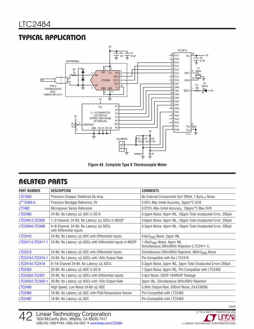
LTC2484
422484ff
For more information www.linear.com/LTC2484
relaTeD parTs
Typical applicaTion
CSSCKSDOSDI
fO
697110
18171615141312112827262524232221
765432
VCC
5V
LTC2484
REF
GNDIN–
IN+
3
ISOTHERMAL
2
C70.1µF
C81µF
C60.1µF
4R22k
5TYPE K
THERMOCOUPLEJACK
(OMEGA MPJ-K-F)
5V
5V
118
GND
RC7RC6RC5RC4RC3RC2RC1RC0RB7RB6RB5RB4RB3RB2RB1RB0RA5RA4RA3RA2RA1RA0
VDD
OSC1
OSC2
MCLR
20
9
10
1
5V
5V
Y16MHz
R110k
D1BAT54
VSS9
2484 F44
VSS19
PIC16F73
D7D6D5D4EN
RWRS
R510k
R410k
R310k
R65k
2
13
2
1
5V
CALIBRATE
CONTRASTGND D0
VCC
D1 D2 D3
2 × 16 CHARACTERLCD DISPLAY
(OPIREX DMC162488OR SIMILAR)
DOWN UP
PART NUMBER DESCRIPTION COMMENTS
LTC1050 Precision Chopper Stabilized Op Amp No External Components 5µV Offset, 1.6µVP-P Noise
LT®1236A-5 Precision Bandgap Reference, 5V 0.05% Max Initial Accuracy, 5ppm/°C Drift
LT1460 Micropower Series Reference 0.075% Max Initial Accuracy, 10ppm/°C Max Drift
LTC2400 24-Bit, No Latency ∆Σ ADC in SO-8 0.3ppm Noise, 4ppm INL, 10ppm Total Unadjusted Error, 200µA
LTC2401/LTC2402 1-/2-Channel, 24-Bit, No Latency ∆Σ ADCs in MSOP 0.6ppm Noise, 4ppm INL, 10ppm Total Unadjusted Error, 200µA
LTC2404/LTC2408 4-/8-Channel, 24-Bit, No Latency ∆Σ ADCs with Differential Inputs
0.3ppm Noise, 4ppm INL, 10ppm Total Unadjusted Error, 200µA
LTC2410 24-Bit, No Latency ∆Σ ADC with Differential Inputs 0.8µVRMS Noise, 2ppm INL
LTC2411/LTC2411-1 24-Bit, No Latency ∆Σ ADCs with Differential Inputs in MSOP 1.45µVRMS Noise, 4ppm INL, Simultaneous 50Hz/60Hz Rejection (LTC2411-1)
LTC2413 24-Bit, No Latency ∆Σ ADC with Differential Inputs Simultaneous 50Hz/60Hz Rejection, 800nVRMS Noise
LTC2415/LTC2415-1 24-Bit, No Latency ∆Σ ADCs with 15Hz Output Rate Pin-Compatible with the LTC2410
LTC2414/LTC2418 8-/16-Channel 24-Bit, No Latency ∆Σ ADCs 0.2ppm Noise, 2ppm INL, 3ppm Total Unadjusted Errors 200µA
LTC2420 20-Bit, No Latency ∆Σ ADC in SO-8 1.2ppm Noise, 8ppm INL, Pin-Compatible with LTC2400
LTC2430/LTC2431 20-Bit, No Latency ∆Σ ADCs with Differential Inputs 2.8µV Noise, SSOP-16/MSOP Package
LTC2435/LTC2435-1 20-Bit, No Latency ∆Σ ADCs with 15Hz Output Rate 3ppm INL, Simultaneous 50Hz/60Hz Rejection
LTC2440 High Speed, Low Noise 24-Bit ∆Σ ADC 3.5kHz Output Rate, 200mV Noise, 24.6 ENOBs
LTC2480 16-Bit, No Latency ∆Σ ADC with PGA/Temperature Sensor Pin-Compatible with LTC2484
LTC2482 16-Bit, No Latency ∆Σ ADC Pin-Compatible with LTC2484
Figure 44. Complete Type K Thermocouple Meter
Linear Technology Corporation1630 McCarthy Blvd., Milpitas, CA 95035-7417 (408) 432-1900 ● FAX: (408) 434-0507 ● www.linear.com/LTC2484 LINEAR TECHNOLOGY CORPORATION 2005
LT 1014 REV F • PRINTED IN USA