ADC Using Discrete Components · 6.101 Final Project Ignacio Estay Forno Abstract Analog to Digital...
23
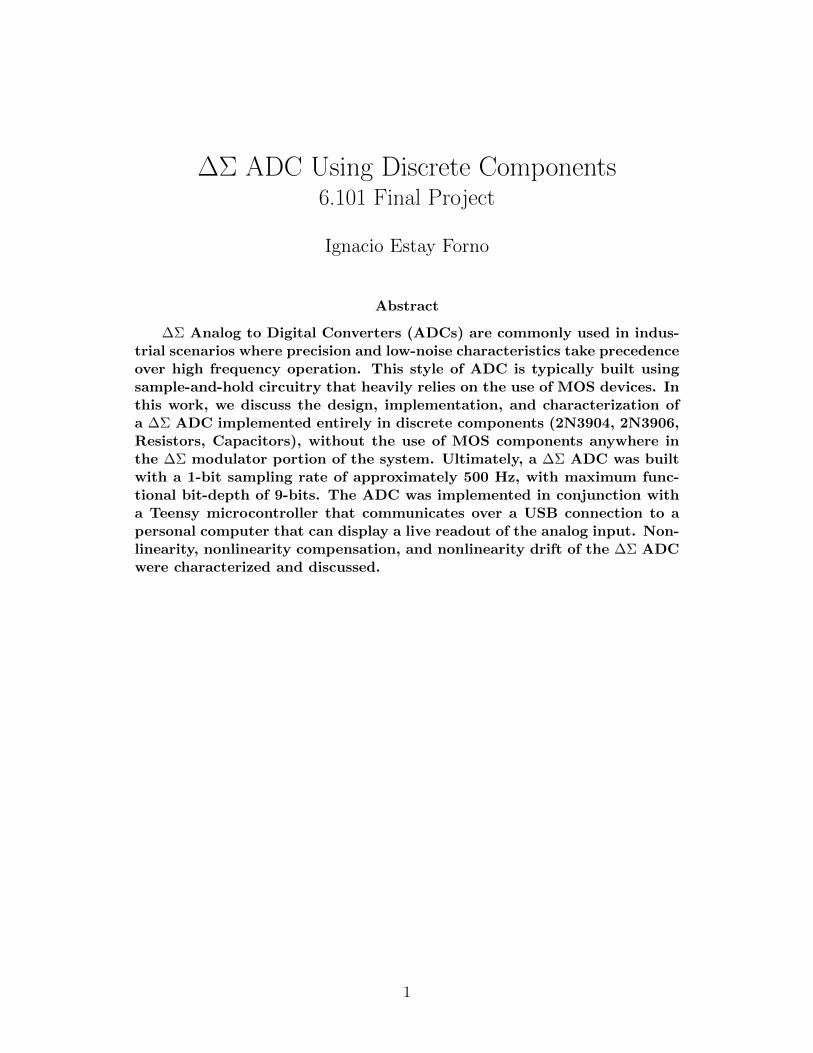
ΔΣ ADC Using Discrete Components 6.101 Final Project Ignacio Estay Forno Abstract ΔΣ Analog to Digital Converters (ADCs) are commonly used in indus- trial scenarios where precision and low-noise characteristics take precedence over high frequency operation. This style of ADC is typically built using sample-and-hold circuitry that heavily relies on the use of MOS devices. In this work, we discuss the design, implementation, and characterization of a ΔΣ ADC implemented entirely in discrete components (2N3904, 2N3906, Resistors, Capacitors), without the use of MOS components anywhere in the ΔΣ modulator portion of the system. Ultimately, a ΔΣ ADC was built with a 1-bit sampling rate of approximately 500 Hz, with maximum func- tional bit-depth of 9-bits. The ADC was implemented in conjunction with a Teensy microcontroller that communicates over a USB connection to a personal computer that can display a live readout of the analog input. Non- linearity, nonlinearity compensation, and nonlinearity drift of the ΔΣ ADC were characterized and discussed. 1
Transcript of ADC Using Discrete Components · 6.101 Final Project Ignacio Estay Forno Abstract Analog to Digital...
∆Σ ADC Using Discrete Components6.101 Final Project
Ignacio Estay Forno
Abstract
∆Σ Analog to Digital Converters (ADCs) are commonly used in indus-trial scenarios where precision and low-noise characteristics take precedenceover high frequency operation. This style of ADC is typically built usingsample-and-hold circuitry that heavily relies on the use of MOS devices. Inthis work, we discuss the design, implementation, and characterization ofa ∆Σ ADC implemented entirely in discrete components (2N3904, 2N3906,Resistors, Capacitors), without the use of MOS components anywhere inthe ∆Σ modulator portion of the system. Ultimately, a ∆Σ ADC was builtwith a 1-bit sampling rate of approximately 500 Hz, with maximum func-tional bit-depth of 9-bits. The ADC was implemented in conjunction witha Teensy microcontroller that communicates over a USB connection to apersonal computer that can display a live readout of the analog input. Non-linearity, nonlinearity compensation, and nonlinearity drift of the ∆Σ ADCwere characterized and discussed.
1
Contents
1 Introduction . . . . . . . . . . . . . . . . . . . . . . . . . . . . . . . . . . . . 51.1 Motivation . . . . . . . . . . . . . . . . . . . . . . . . . . . . . . . . . 51.2 Design Goals . . . . . . . . . . . . . . . . . . . . . . . . . . . . . . . 6
2 Resources . . . . . . . . . . . . . . . . . . . . . . . . . . . . . . . . . . . . . 73 Design Walk-through . . . . . . . . . . . . . . . . . . . . . . . . . . . . . . . 7
3.1 Input (OTA) and Integrator (INT) . . . . . . . . . . . . . . . . . . . 83.2 Comparator (CMP) and Sample-Hold . . . . . . . . . . . . . . . . . . 93.3 1-bit DAC . . . . . . . . . . . . . . . . . . . . . . . . . . . . . . . . . 113.4 Digital Functions (Teensy) . . . . . . . . . . . . . . . . . . . . . . . . 123.5 Bias Cell . . . . . . . . . . . . . . . . . . . . . . . . . . . . . . . . . . 12
4 Implementation Notes . . . . . . . . . . . . . . . . . . . . . . . . . . . . . . 144.1 Hardware . . . . . . . . . . . . . . . . . . . . . . . . . . . . . . . . . 144.2 Software . . . . . . . . . . . . . . . . . . . . . . . . . . . . . . . . . . 15
5 Results . . . . . . . . . . . . . . . . . . . . . . . . . . . . . . . . . . . . . . . 175.1 Sinusoidal Response . . . . . . . . . . . . . . . . . . . . . . . . . . . 185.2 Step Response . . . . . . . . . . . . . . . . . . . . . . . . . . . . . . . 205.3 Bit-Depth and Bandwidth . . . . . . . . . . . . . . . . . . . . . . . . 22
6 Conclusion . . . . . . . . . . . . . . . . . . . . . . . . . . . . . . . . . . . . . 23
2
List of Figures
1 Block diagram of proposed signal chain . . . . . . . . . . . . . . . . . . . . . 82 Schematic for the OTA and integrator stage . . . . . . . . . . . . . . . . . . 93 Schematic for the Sample-hold and CMP stage . . . . . . . . . . . . . . . . . 104 Schematic for the DAC stage . . . . . . . . . . . . . . . . . . . . . . . . . . . 115 Schematic of the bias cell . . . . . . . . . . . . . . . . . . . . . . . . . . . . . 136 Graph displaying the input vs output nonlinearity for the ADC . . . . . . . 157 0.5 Hz sine wave captured with 4-bit, 8-bit, and 9-bit resolution. . . . . . . . 198 0.5 Hz square wave captured with 4-bit, 8-bit, and 9-bit resolution. . . . . . 219 6 Vpp, 1 Hz −→ 5 Hz sweep in 6-bit and 8-bit resolution. . . . . . . . . . . . 22
3

List of Tables
1 Possible Result Specifications . . . . . . . . . . . . . . . . . . . . . . . . . . 62 Expected components use and unit costs . . . . . . . . . . . . . . . . . . . . 7
4
1 Introduction
1.1 Motivation
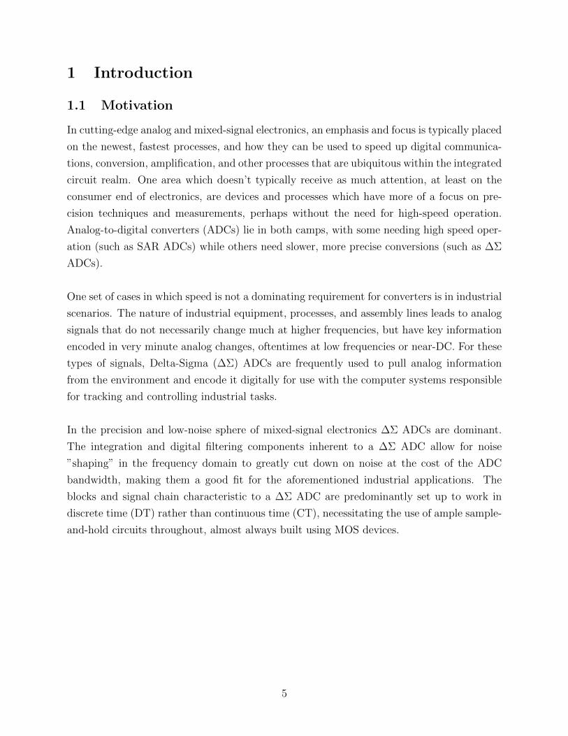
In cutting-edge analog and mixed-signal electronics, an emphasis and focus is typically placed
on the newest, fastest processes, and how they can be used to speed up digital communica-
tions, conversion, amplification, and other processes that are ubiquitous within the integrated
circuit realm. One area which doesn’t typically receive as much attention, at least on the
consumer end of electronics, are devices and processes which have more of a focus on pre-
cision techniques and measurements, perhaps without the need for high-speed operation.
Analog-to-digital converters (ADCs) lie in both camps, with some needing high speed oper-
ation (such as SAR ADCs) while others need slower, more precise conversions (such as ∆Σ
ADCs).
One set of cases in which speed is not a dominating requirement for converters is in industrial
scenarios. The nature of industrial equipment, processes, and assembly lines leads to analog
signals that do not necessarily change much at higher frequencies, but have key information
encoded in very minute analog changes, oftentimes at low frequencies or near-DC. For these
types of signals, Delta-Sigma (∆Σ) ADCs are frequently used to pull analog information
from the environment and encode it digitally for use with the computer systems responsible
for tracking and controlling industrial tasks.
In the precision and low-noise sphere of mixed-signal electronics ∆Σ ADCs are dominant.
The integration and digital filtering components inherent to a ∆Σ ADC allow for noise
”shaping” in the frequency domain to greatly cut down on noise at the cost of the ADC
bandwidth, making them a good fit for the aforementioned industrial applications. The
blocks and signal chain characteristic to a ∆Σ ADC are predominantly set up to work in
discrete time (DT) rather than continuous time (CT), necessitating the use of ample sample-
and-hold circuits throughout, almost always built using MOS devices.
5
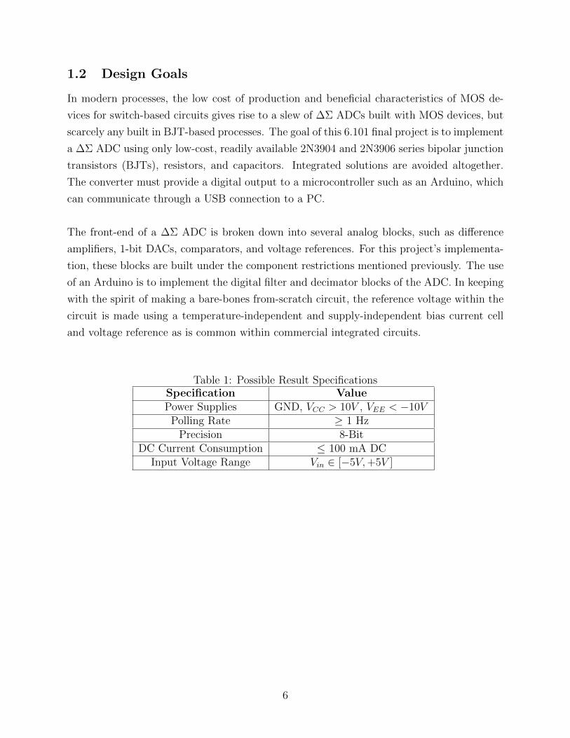
1.2 Design Goals
In modern processes, the low cost of production and beneficial characteristics of MOS de-
vices for switch-based circuits gives rise to a slew of ∆Σ ADCs built with MOS devices, but
scarcely any built in BJT-based processes. The goal of this 6.101 final project is to implement
a ∆Σ ADC using only low-cost, readily available 2N3904 and 2N3906 series bipolar junction
transistors (BJTs), resistors, and capacitors. Integrated solutions are avoided altogether.
The converter must provide a digital output to a microcontroller such as an Arduino, which
can communicate through a USB connection to a PC.
The front-end of a ∆Σ ADC is broken down into several analog blocks, such as difference
amplifiers, 1-bit DACs, comparators, and voltage references. For this project’s implementa-
tion, these blocks are built under the component restrictions mentioned previously. The use
of an Arduino is to implement the digital filter and decimator blocks of the ADC. In keeping
with the spirit of making a bare-bones from-scratch circuit, the reference voltage within the
circuit is made using a temperature-independent and supply-independent bias current cell
and voltage reference as is common within commercial integrated circuits.
Table 1: Possible Result SpecificationsSpecification ValuePower Supplies GND, VCC > 10V , VEE < −10V
Polling Rate ≥ 1 HzPrecision 8-Bit
DC Current Consumption ≤ 100 mA DCInput Voltage Range Vin ∈ [−5V,+5V ]
6
2 Resources
All the resources mentioned used in this project are both low-cost in bulk, and already
available within the 6.101 and EDS parts libraries. Table 2 displays the set of components,
approximate amounts used, and bulk unit cost of the individual components that make up
the project. The project will be built on breadboards.
Table 2: Expected components use and unit costsComponent Amount Bulk Unit Cost (Digikey)
2N3904 Transistor ≈ 25 $0.052N3906 Transistor ≈ 25 $0.041/4 Watt Resistors ≈ 30 $0.01Assorted Capacitors ≈ 20 Varies
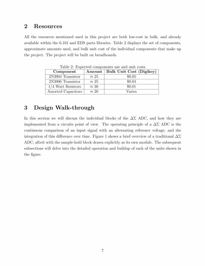
3 Design Walk-through
In this section we will discuss the individual blocks of the ∆Σ ADC, and how they are
implemented from a circuits point of view. The operating principle of a ∆Σ ADC is the
continuous comparison of an input signal with an alternating reference voltage, and the
integration of this difference over time. Figure 1 shows a brief overview of a traditional ∆Σ
ADC, albeit with the sample-hold block drawn explicitly as its own module. The subsequent
subsections will delve into the detailed operation and buildup of each of the units shown in
the figure.
7
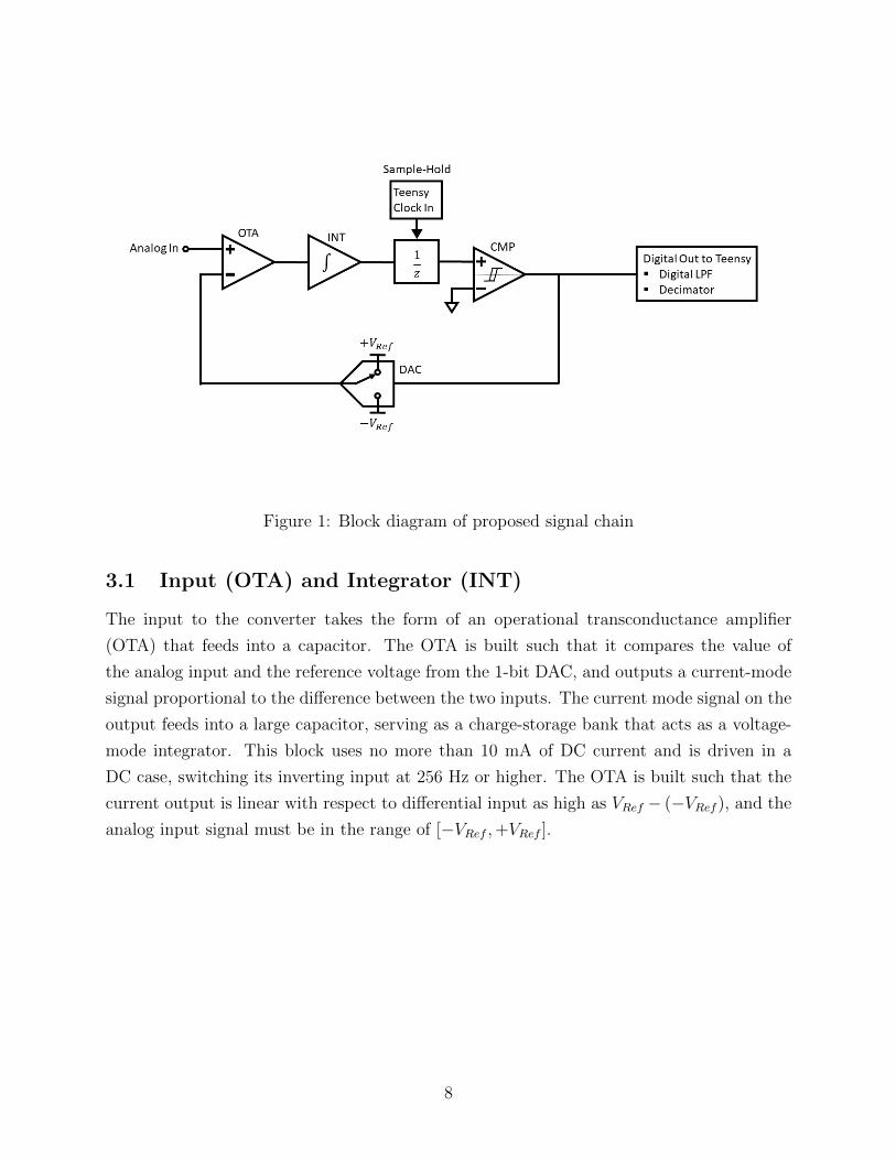
Figure 1: Block diagram of proposed signal chain
3.1 Input (OTA) and Integrator (INT)
The input to the converter takes the form of an operational transconductance amplifier
(OTA) that feeds into a capacitor. The OTA is built such that it compares the value of
the analog input and the reference voltage from the 1-bit DAC, and outputs a current-mode
signal proportional to the difference between the two inputs. The current mode signal on the
output feeds into a large capacitor, serving as a charge-storage bank that acts as a voltage-
mode integrator. This block uses no more than 10 mA of DC current and is driven in a
DC case, switching its inverting input at 256 Hz or higher. The OTA is built such that the
current output is linear with respect to differential input as high as VRef − (−VRef ), and the
analog input signal must be in the range of [−VRef ,+VRef ].
8
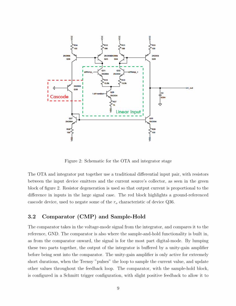
Figure 2: Schematic for the OTA and integrator stage
The OTA and integrator put together use a traditional differential input pair, with resistors
between the input device emitters and the current source’s collector, as seen in the green
block of figure 2. Resistor degeneration is used so that output current is proportional to the
difference in inputs in the large signal case. The red block highlights a ground-referenced
cascode device, used to negate some of the ro characteristic of device Q36.
3.2 Comparator (CMP) and Sample-Hold
The comparator takes in the voltage-mode signal from the integrator, and compares it to the
reference, GND. The comparator is also where the sample-and-hold functionality is built in,
as from the comparator onward, the signal is for the most part digital-mode. By lumping
these two parts together, the output of the integrator is buffered by a unity-gain amplifier
before being sent into the comparator. The unity-gain amplifier is only active for extremely
short durations, when the Teensy ”pulses” the loop to sample the current value, and update
other values throughout the feedback loop. The comparator, with the sample-hold block,
is configured in a Schmitt trigger configuration, with slight positive feedback to allow it to
9
hold whatever output it switched to when the Teensy pulsed the unity-gain amplifier from
INT to CMP on.
Figure 3 displays the schematics for the sample-hold and the comparator segments of the
pipeline. This consists of a rudimentary op-amp buffer for the sampling stage, and a Schmitt
trigger comparator made using a similar op-amp topology.
Figure 3: Schematic for the Sample-hold and CMP stage
The green block shows a pulsed current source. Within the circuit, this manifests itself as a
Teensy output that has a digital, 0V − 5V signal that pulses at roughly 500 Hz, with a duty
cycle of 1%. This pulses the current on and off throughout the op-amp buffer, temporarily
giving it current drive capability whenever the Teensy is outputting a high signal. This
buffer’s output is tied to a capacitor, such that when the Teensy output is low, the value is
held to some degree, as the buffer’s current drive capability goes to 0.
The red block on the comparator shows how the comparator is set up in the Schmitt trigger.
When the buffer is turned on, and has current drive capability, the voltage divider at the
input of the comparator is preferentially driven to the value at the output of the buffer.
As the buffer is turned off, and its current drive capability is reduced to 0, the output
of the comparator becomes the dominant voltage and current source for the input of the
comparator. This positive feedback path keeps the output of the comparator latched to
whatever value it was at before the buffer was turned off. This latching function keeps the
comparator at this value until the buffer is turned on again, at which point the comparator
10
updates to whatever new value it should be at based upon the input to the buffer and
comparator.
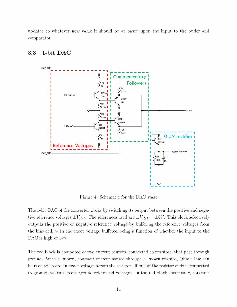
3.3 1-bit DAC
Figure 4: Schematic for the DAC stage
The 1-bit DAC of the converter works by switching its output between the positive and nega-
tive reference voltages ±VRef . The references used are ±VRef = ±5V . This block selectively
outputs the positive or negative reference voltage by buffering the reference voltages from
the bias cell, with the exact voltage buffered being a function of whether the input to the
DAC is high or low.
The red block is composed of two current sources, connected to resistors, that pass through
ground. With a known, constant current source through a known resistor, Ohm’s law can
be used to create an exact voltage across the resistor. If one of the resistor ends is connected
to ground, we can create ground-referenced voltages. In the red block specifically, constant
11
current sources are used to create ±4.3V sources.
The green block holds the complementary followers. In order to understand their func-
tion, we need to observe the previous module, the Schmitt trigger comparator, as a current
source that either acts as a current drain towards VEE, or a current source that sources
current from VCC . When the comparator is outputting high, the top half of the circuit
activates, and creates an emitter-follower circuit through device Q22 by pulling a fixed cur-
rent through its emitter, with its emitter outputting 4.3V + 0.7V = +5V to the DAC OUT
node. While this is happening, the comparator output node is high enough that device Q21
stays off, not conducting. When the comparator output is low, the same happens, but in
complementary fashion, with device Q22 being off, and device Q21 being active, presenting
a −4.3V − 0.7V = −5V low impedance output to the DAC OUT node.
The blue block encloses the rectifier portion of the DAC. This module ensures that its
output can only see positive values above ground, by using a BJT as a diode, into a pull
down resistor. When the DAC outputs +5, current passes through the BJT diode, and
charges the node up to almost 5V, when considering the diode drop. The output node of
this block goes into a digital input of the Teensy.
3.4 Digital Functions (Teensy)
A Teensy microcontroller is used to read the digital signal from the sample and hold block
on every cycle. The Teensy is programmed to perform a digital low-pass filter on the data
entering it, by some form of averaging function of the last N digital samples, and then
convert this value to a typical digital representation, subsequently outputting the result to
a PC via a USB serial connection.
3.5 Bias Cell
A rudimentary supply-independent bias cell is constructed, taking advantage of the diode-like
characteristics and load-lines of 2N3904/2N3906 devices with bases and collectors attached
to each other. This cell functions mostly independent of applied power supply voltages, and
will be used to create static, well-controlled DC bias currents and reference voltages that
drive the rest of the converter’s blocks.
12
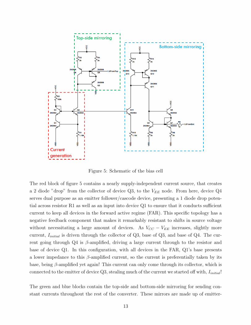
Figure 5: Schematic of the bias cell
The red block of figure 5 contains a nearly supply-independent current source, that creates
a 2 diode ”drop” from the collector of device Q3, to the VEE node. From here, device Q4
serves dual purpose as an emitter follower/cascode device, presenting a 1 diode drop poten-
tial across resistor R1 as well as an input into device Q1 to ensure that it conducts sufficient
current to keep all devices in the forward active regime (FAR). This specific topology has a
negative feedback component that makes it remarkably resistant to shifts in source voltage
without necessitating a large amount of devices. As VCC − VEE increases, slightly more
current, Iinitial is driven through the collector of Q3, base of Q3, and base of Q4. The cur-
rent going through Q4 is β-amplified, driving a large current through to the resistor and
base of device Q1. In this configuration, with all devices in the FAR, Q1’s base presents
a lower impedance to this β-amplified current, so the current is preferentially taken by its
base, being β-amplified yet again! This current can only come through its collector, which is
connected to the emitter of device Q3, stealing much of the current we started off with, Iinitial!
The green and blue blocks contain the top-side and bottom-side mirroring for sending con-
stant currents throughout the rest of the converter. These mirrors are made up of emitter-
13
degenerated Wilson current mirrors to negate the effects of finite β values and improve
current matching.
4 Implementation Notes
4.1 Hardware
OTA Mismatch
As the OTA is the first step in the signal chain, any mismatch or nonidealities in it get
cascaded down throughout the entire system. In order to mitigate mismatch and input
offset for the OTA, a small potentiometer was used in place of R28 in figure 2 to adjust
output currents such that the input-referred offset of the OTA goes to 0.
Sampling
The internal timing of the Teensy makes it difficult to send low-jitter, consistent-length
digital pulses in the µs length, as each command in the Arduino code can take a variable
amount of time to complete. For instance, a digital high command followed directly by
a digital low command can produce a pulse of length anywhere from 15µs to 25µs. As a
workaround for this, Arduino’s analogWrite(pin,val) function was used. Contrary to its
name, this function does not actually output an analog value, but rather outputs a pulse-
width-modulated (PWM) signal, with a frequency of 488.28 Hz, a value of 0V or 5V, and a
duty cycle of val/256. The analogWrite function runs in the background, constantly, after
being set, so it was perfect as a background clock by which the ADC could be pulsed.
Schmitt Trigger
As expected, during construction and subsequent testing, the sample-hold and Schmitt trig-
ger blocks were the most difficult to get to work ”properly.” To ease this, a potentiometer
was used to help fine-tune the feedback ratio from the output of the comparator such that
the system as a whole could work properly, without giving a false reading by discharging the
filter capacitor at the output of the sample-hold buffer.
14
4.2 Software
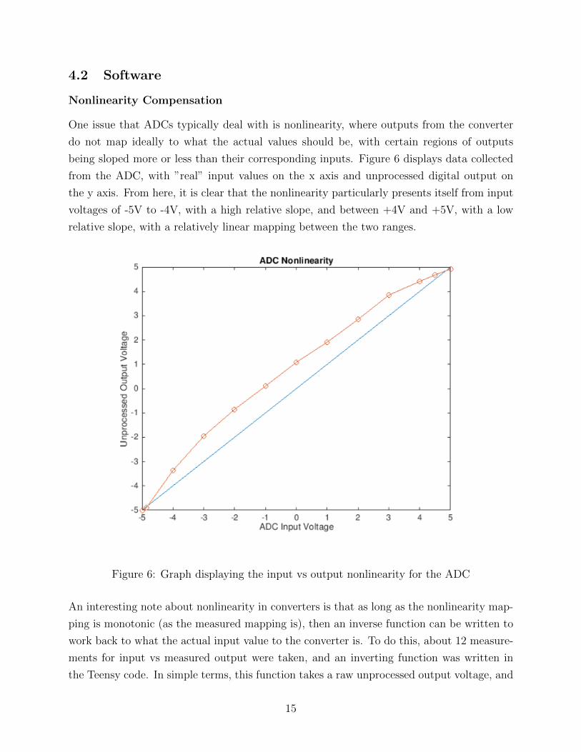
Nonlinearity Compensation
One issue that ADCs typically deal with is nonlinearity, where outputs from the converter
do not map ideally to what the actual values should be, with certain regions of outputs
being sloped more or less than their corresponding inputs. Figure 6 displays data collected
from the ADC, with ”real” input values on the x axis and unprocessed digital output on
the y axis. From here, it is clear that the nonlinearity particularly presents itself from input
voltages of -5V to -4V, with a high relative slope, and between +4V and +5V, with a low
relative slope, with a relatively linear mapping between the two ranges.
Figure 6: Graph displaying the input vs output nonlinearity for the ADC
An interesting note about nonlinearity in converters is that as long as the nonlinearity map-
ping is monotonic (as the measured mapping is), then an inverse function can be written to
work back to what the actual input value to the converter is. To do this, about 12 measure-
ments for input vs measured output were taken, and an inverting function was written in
the Teensy code. In simple terms, this function takes a raw unprocessed output voltage, and
15
references the vertical value from figure 6, finding the intersection point, and looks for the
point directly below it to calculate what the actual input value was. This nonlinearity com-
pensation worked surprisingly well in practice, allowing for digital outputs typically closer
than about 0.1V from analog inputs. This compensation does have the unfortunate effect of
skewing the effective voltage-mode resolution, providing more resolution around the -5V to
-4V range in this example, and less resolution in the +4V to +5V range.
Nonlinearity Drift
After leaving the ADC for several days, then coming back to it to take more samples,
it appears as if the nonlinearity profile was not constant compared to the one previously
discussed in figure 6. Specifically, the nonlinearity differed in the lowest and highest parts
of the ADC input voltage, however the middle range remained relatively linear all things
considered. The root cause of this is unknown, but the current hypothesis is that it is due
to some form of temperature dependence in the latching behavior of the sample and hold
module.
16
5 Results
The figures within this section each serve to display different characteristics of the ADC
developed, and how those characteristics change as a function of ADC resolution. Since a
∆Σ ADC functions based on taking a rolling average of samples, the higher the bit depth,
the more samples need to be taken to acquire a reading. If the system refresh rate is fixed,
then there is an inherent bandwidth limit that is intimately tied to the bit depth chosen for
the ADC to operate at. Choosing too high of a bit depth or bandwidth respectively will
cause degradation in ”real” bandwidth and precision, respectively.
17
5.1 Sinusoidal Response
Figure 7 displays the output of the ADC with a 6 Vpp, 0.5 Hz sine wave input at 4, 8, and 9
bit resolution. Of note is the more discrete steps in the lower resolutions, and the occasional
”glitch” where a noisy sample sends a sample too high or too low compared to what the
ideally sampled sine wave might have looked like after 4-bit sampling. These glitches in either
direction, along with the quantization noise, are very much reduced when observing an input
at higher sampling resolutions. For low frequency signals, higher bit-depth resolution greatly
improve the signal recreation capabilities of this ADC.
18
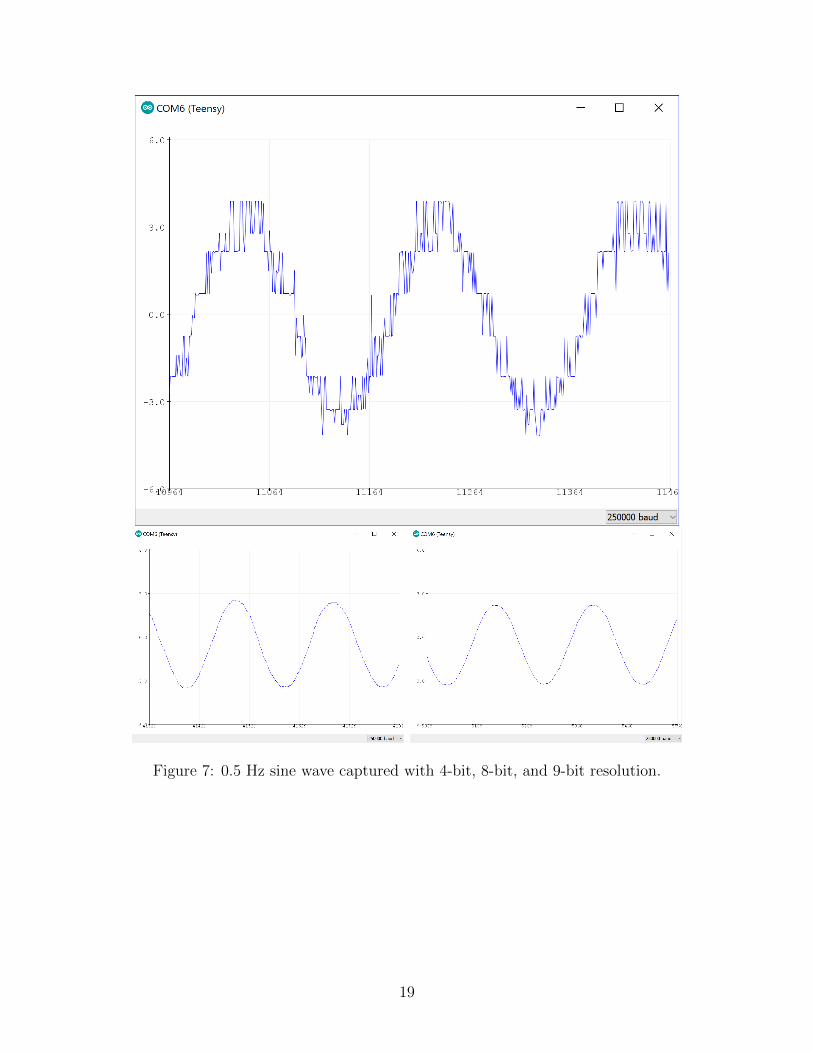
Figure 7: 0.5 Hz sine wave captured with 4-bit, 8-bit, and 9-bit resolution.
19
5.2 Step Response
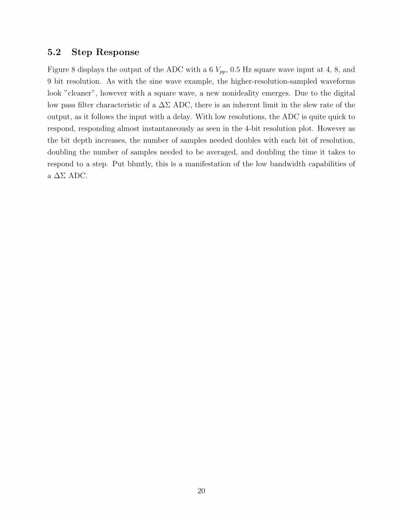
Figure 8 displays the output of the ADC with a 6 Vpp, 0.5 Hz square wave input at 4, 8, and
9 bit resolution. As with the sine wave example, the higher-resolution-sampled waveforms
look ”cleaner”, however with a square wave, a new nonideality emerges. Due to the digital
low pass filter characteristic of a ∆Σ ADC, there is an inherent limit in the slew rate of the
output, as it follows the input with a delay. With low resolutions, the ADC is quite quick to
respond, responding almost instantaneously as seen in the 4-bit resolution plot. However as
the bit depth increases, the number of samples needed doubles with each bit of resolution,
doubling the number of samples needed to be averaged, and doubling the time it takes to
respond to a step. Put bluntly, this is a manifestation of the low bandwidth capabilities of
a ∆Σ ADC.
20
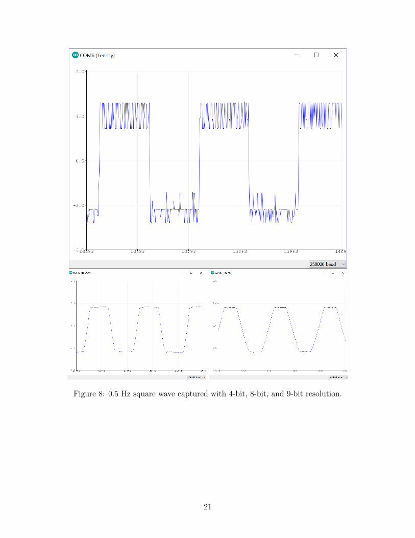
Figure 8: 0.5 Hz square wave captured with 4-bit, 8-bit, and 9-bit resolution.
21
5.3 Bit-Depth and Bandwidth
Figure 9 displays a 1Hz to 5Hz 6 Vpp sine wave sweep over 5 seconds. In one case the
amplifier is set to 6-bit resolution and in the other it is set to 8-bit. In addition to the
phenomenon discussed with regards to the pure sine and square plots, this plot more clearly
shows the bandwidth limitations of a ∆Σ ADC operating at higher resolutions, and the
necessity for choosing the adequate resolution for the use case. In this example, the 6-bit
sampling faithfully recreates the entire wave sweep without much attenuation, whereas the
8-bit sampling quickly declines in amplitude with respect to frequency, even exhibiting what
looks to be aliasing at the higher frequencies, where the effective sampling frequency (a
function of resolution and ADC clock) is less than the required Nyquist sampling frequency.
Figure 9: 6 Vpp, 1 Hz −→ 5 Hz sweep in 6-bit and 8-bit resolution.
22
6 Conclusion
In this work we have demonstrated the construction of a ∆Σ ADC using only discrete,
low cost components. Through design, simulation, building, and troubleshooting, the ∆Σ
modulator was integrated into a system as a whole that utilized a Teensy microcontroller
to interface with a personal computer. The key accomplishment made was in the realm of
integrating the entire system as an IC-style system, allowing for arbitrary supply inputs, an
internal biasing scheme, and consistent operation for the end user. Future work could focus
on eliminating the nonlinearity of the system and increasing its sampling bandwidth.
23