
Ten Output High Performance Clock Synchronizer, … · Ten Output High Performance Clock...
78
CDCE72010 www.ti.com SCAS858C – JUNE 2008 – REVISED JANUARY 2012 Ten Output High Performance Clock Synchronizer, Jitter Cleaner, and Clock Distributor Check for Samples: CDCE72010 1FEATURES • Wide Charge-Pump Current Range From 200μA to 3mA • High Performance LVPECL, LVDS, LVCMOS • Presets Charge-Pump to V CC_CP /2 for Fast PLL Clock Synchronizer Center-Frequency Setting of VC(X)O, • Two Reference Clock Inputs (Primary and Controlled Via the SPI Bus Secondary Clock) for Redundancy Support • SERDES Startup Mode (Depending on VCXO with Manual or Automatic Selection Range) • Accepts Two Differential Input (LVPECL or • Auxiliary Input: Output 9 can Serve as 2nd LVDS) References up to 500MHz (or Two VCXO Input to Drive All Outputs or to Serve as LVCMOS Inputs up to 250MHz) as PLL PLL Feedback Signal Reference • RESET or HOLD Input Pin to Serve as Reset or • VCXO_IN Clock is Synchronized to One of Two Hold Functions Reference Clocks • REFERENCE SELECT for Manual Select • VCXO_IN Frequencies up to 1.5GHz (LVPECL) Between Primary and Secondary Reference 800MHz for LVDS and 250MHz for LVCMOS Clocks Level Signaling • POWER DOWN (PD) to Put Device in Standby • Outputs Can be a Combination of LVPECL, Mode LVDS, and LVCMOS (Up to 10 Differential LVPECL or LVDS Outputs or up to 20 LVCMOS • Analog and Digital PLL Lock Indicator Outputs), Output 9 can be Converted to an • Internally Generated VBB Bias Voltages for Auxiliary Input as a 2nd VC(X)O. Single-Ended Input Signals • Output Divider is Selectable to Divide by 1, 2, • Frequency Hold-Over Mode Activated by 3, 4, 5, 6, 8, 10, 12, 16, 18, 20, 24, 28, 30, 32, 36, HOLD Pin or SPI Bus to Improve Fail-Safe 40, 42, 48, 50, 56, 60, 64, 70, or 80 On Each Operation Output Individually up to Eight Dividers. • Input to All Outputs Skew Control (Except for Output 0 and 9, Output 0 Follows • Individual Skew Control for Each Output with Output 1 Divider and Output 9 Follows Output Each Output Divider 8 Divider) • Packaged in a QFN-64 Package • SPI Controllable Device Setting • ESD Protection Exceeds 2kV HBM • Individual Output Enable Control via SPI • Industrial Temperature Range of –40°C to 85° Interface • Integrated On-Chip Non-Volatile Memory APPLICATIONS (EEPROM) to Store Settings without the Need to Apply High Voltage to the Device • Low Jitter Clock Driver for High-End Telecom and Wireless Applications • Optional Configuration Pins to Select Between Two Default Settings Stored in EEPROM • High Precision Test Equipment • Efficient Jitter Cleaning from Low PLL Loop Bandwidth • Very Low Phase Noise PLL Core • Programmable Phase Offset (Input Reference to Outputs) 1 Please be aware that an important notice concerning availability, standard warranty, and use in critical applications of Texas Instruments semiconductor products and disclaimers thereto appears at the end of this data sheet. PRODUCTION DATA information is current as of publication date. Copyright © 2008–2012, Texas Instruments Incorporated Products conform to specifications per the terms of the Texas Instruments standard warranty. Production processing does not necessarily include testing of all parameters.
Transcript of Ten Output High Performance Clock Synchronizer, … · Ten Output High Performance Clock...
CDCE72010
www.ti.com SCAS858C –JUNE 2008–REVISED JANUARY 2012
Ten Output High Performance Clock Synchronizer, Jitter Cleaner, and Clock DistributorCheck for Samples: CDCE72010
1FEATURES • Wide Charge-Pump Current Range From200μA to 3mA• High Performance LVPECL, LVDS, LVCMOS
• Presets Charge-Pump to VCC_CP/2 for FastPLL Clock SynchronizerCenter-Frequency Setting of VC(X)O,• Two Reference Clock Inputs (Primary andControlled Via the SPI BusSecondary Clock) for Redundancy Support
• SERDES Startup Mode (Depending on VCXOwith Manual or Automatic SelectionRange)• Accepts Two Differential Input (LVPECL or
• Auxiliary Input: Output 9 can Serve as 2ndLVDS) References up to 500MHz (or TwoVCXO Input to Drive All Outputs or to Serve asLVCMOS Inputs up to 250MHz) as PLLPLL Feedback SignalReference
• RESET or HOLD Input Pin to Serve as Reset or• VCXO_IN Clock is Synchronized to One of TwoHold FunctionsReference Clocks
• REFERENCE SELECT for Manual Select• VCXO_IN Frequencies up to 1.5GHz (LVPECL)Between Primary and Secondary Reference800MHz for LVDS and 250MHz for LVCMOSClocksLevel Signaling
• POWER DOWN (PD) to Put Device in Standby• Outputs Can be a Combination of LVPECL,ModeLVDS, and LVCMOS (Up to 10 Differential
LVPECL or LVDS Outputs or up to 20 LVCMOS • Analog and Digital PLL Lock IndicatorOutputs), Output 9 can be Converted to an • Internally Generated VBB Bias Voltages forAuxiliary Input as a 2nd VC(X)O. Single-Ended Input Signals
• Output Divider is Selectable to Divide by 1, 2, • Frequency Hold-Over Mode Activated by3, 4, 5, 6, 8, 10, 12, 16, 18, 20, 24, 28, 30, 32, 36, HOLD Pin or SPI Bus to Improve Fail-Safe40, 42, 48, 50, 56, 60, 64, 70, or 80 On Each OperationOutput Individually up to Eight Dividers. • Input to All Outputs Skew Control(Except for Output 0 and 9, Output 0 Follows
• Individual Skew Control for Each Output withOutput 1 Divider and Output 9 Follows OutputEach Output Divider8 Divider)
• Packaged in a QFN-64 Package• SPI Controllable Device Setting• ESD Protection Exceeds 2kV HBM• Individual Output Enable Control via SPI• Industrial Temperature Range of –40°C to 85°Interface
• Integrated On-Chip Non-Volatile MemoryAPPLICATIONS(EEPROM) to Store Settings without the Need
to Apply High Voltage to the Device • Low Jitter Clock Driver for High-End Telecomand Wireless Applications• Optional Configuration Pins to Select Between
Two Default Settings Stored in EEPROM • High Precision Test Equipment• Efficient Jitter Cleaning from Low PLL Loop
Bandwidth• Very Low Phase Noise PLL Core• Programmable Phase Offset (Input Reference
to Outputs)
1
Please be aware that an important notice concerning availability, standard warranty, and use in critical applications of TexasInstruments semiconductor products and disclaimers thereto appears at the end of this data sheet.
PRODUCTION DATA information is current as of publication date. Copyright © 2008–2012, Texas Instruments IncorporatedProducts conform to specifications per the terms of the TexasInstruments standard warranty. Production processing does notnecessarily include testing of all parameters.
PFD
ChargePump
PRI_REFN
SEC_REF
AAuuxxiilliiaarryy IInnppuutt
VCXO/ VCO IN
EEPROM
Output Divider 1
U0N
U0P
U1N
U1P
U2N
U2P
U3N
U3P
U4N
U4P
U5N
U5P
U6N
U6P
U7N
U7P
U8N
U8P
U9N or AUXINN
U9P or AUX INP
Output Divider 2
Output Divider 3
Output Divider 4
Output Divider 5
Output Divider 6
Output Divider 7
Output Divider 8
PLL_LOCKREF_SEL
PDRESET HOLDor
MODE_SEL
AUX_SEL
SPI_MISOSPI_LE (CD1)
SPI_CLK (CD2)SPI_MOSI (CD3)
Interface& Control
FeedbackDivider
CDCE72010
SCAS858C –JUNE 2008–REVISED JANUARY 2012 www.ti.com
These devices have limited built-in ESD protection. The leads should be shorted together or the device placed in conductive foamduring storage or handling to prevent electrostatic damage to the MOS gates.
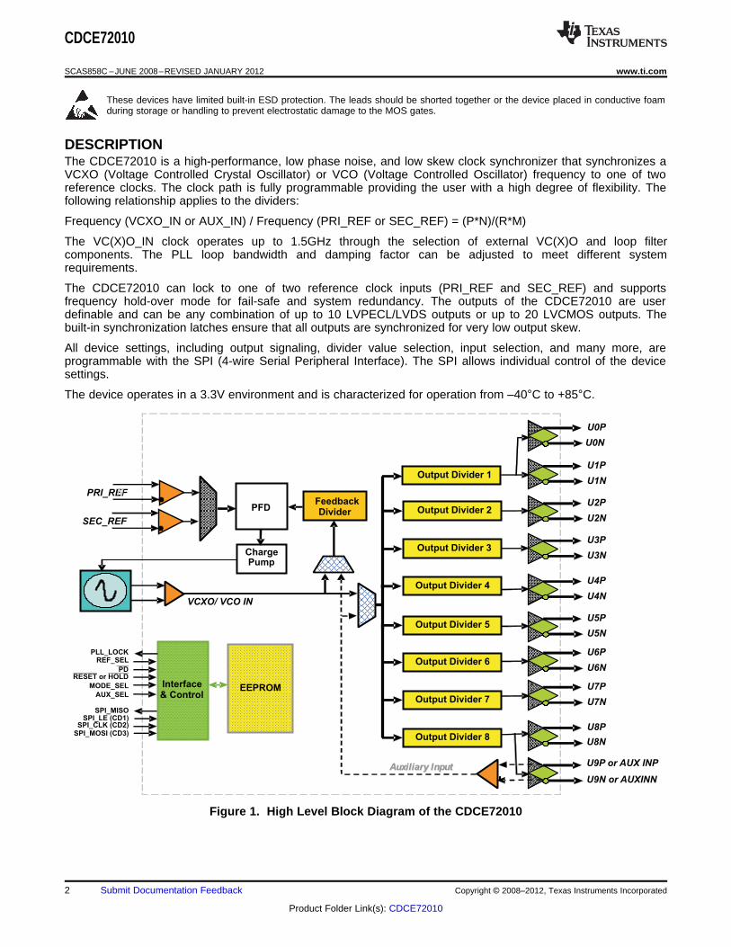
DESCRIPTIONThe CDCE72010 is a high-performance, low phase noise, and low skew clock synchronizer that synchronizes aVCXO (Voltage Controlled Crystal Oscillator) or VCO (Voltage Controlled Oscillator) frequency to one of tworeference clocks. The clock path is fully programmable providing the user with a high degree of flexibility. Thefollowing relationship applies to the dividers:
Frequency (VCXO_IN or AUX_IN) / Frequency (PRI_REF or SEC_REF) = (P*N)/(R*M)
The VC(X)O_IN clock operates up to 1.5GHz through the selection of external VC(X)O and loop filtercomponents. The PLL loop bandwidth and damping factor can be adjusted to meet different systemrequirements.
The CDCE72010 can lock to one of two reference clock inputs (PRI_REF and SEC_REF) and supportsfrequency hold-over mode for fail-safe and system redundancy. The outputs of the CDCE72010 are userdefinable and can be any combination of up to 10 LVPECL/LVDS outputs or up to 20 LVCMOS outputs. Thebuilt-in synchronization latches ensure that all outputs are synchronized for very low output skew.
All device settings, including output signaling, divider value selection, input selection, and many more, areprogrammable with the SPI (4-wire Serial Peripheral Interface). The SPI allows individual control of the devicesettings.
The device operates in a 3.3V environment and is characterized for operation from –40°C to +85°C.
Figure 1. High Level Block Diagram of the CDCE72010
2 Submit Documentation Feedback Copyright © 2008–2012, Texas Instruments Incorporated
Product Folder Link(s): CDCE72010
1
64 63 62 61 5060 59 58 57 56 55 54 53 52 51 49
48
47
46
45
44
43
42
41
40
39
38
37
36
35
34
33
32313029282726252423222120191817
16
15
14
13
12
11
10
2
3
4
5
6
7
8
9
TESTOUTA
GND_CP
CP_OUT
VCC_PLL
VCC
U0N
U0P
VCC
U1N
U1P
VCC
U2N
U2P
VCC
SPI_MISO
MODE_SEL
PD
AU
X_S
EL
VC
C
U3N
U3P
VC
C
U4N
U4P
VC
C
U5N
U5P
VC
C
U6N
U6P
VC
C
GN
D
RESET
VCC
U7N
U7P
VCC
U8N
U8P
VCC
U9N
U9P
VCC
SPI_MOIS
SPI_LE
SPI_CLK
REF_SEL
VCCA
VC
CA
PLL_LO
CK
VC
C_V
CX
O
VC
XO
_IN
-
VC
XO
_IN
+
VC
C_V
CX
O
STA
TU
S
VB
B
VC
C_IN
PR
I_R
EF
-
PR
I_R
EF
+
VC
C_IN
SE
C_R
EF
-
SE
C_R
EF
+
VC
C_P
LL
VC
C_C
P
CDCE72010(Top View)
CDCE72010
www.ti.com SCAS858C –JUNE 2008–REVISED JANUARY 2012
Copyright © 2008–2012, Texas Instruments Incorporated Submit Documentation Feedback 3
Product Folder Link(s): CDCE72010
49
1
32
64
3348
16
17
Top View
Bottom View
CDCE72010
SCAS858C –JUNE 2008–REVISED JANUARY 2012 www.ti.com
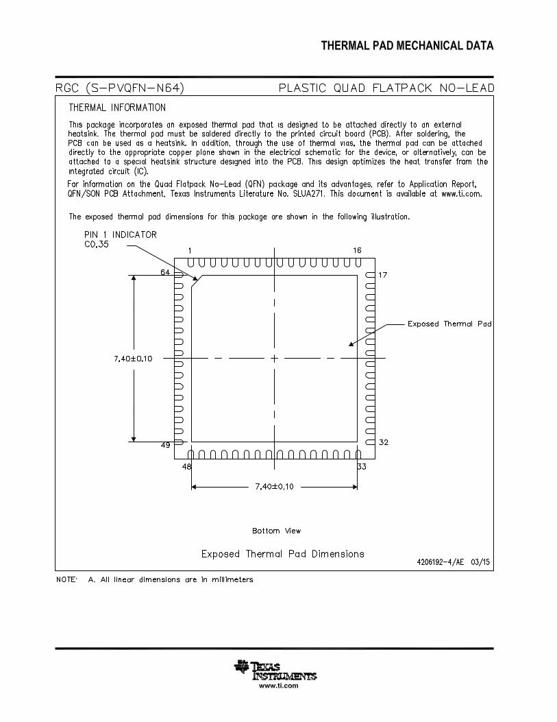
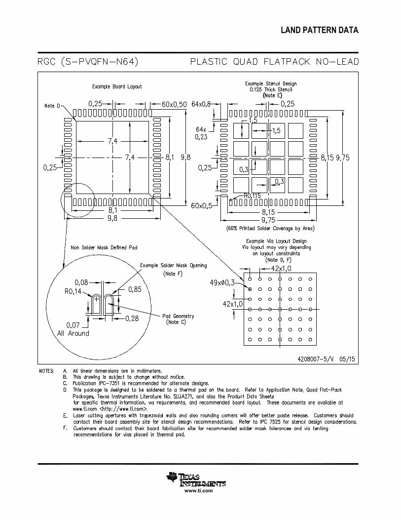
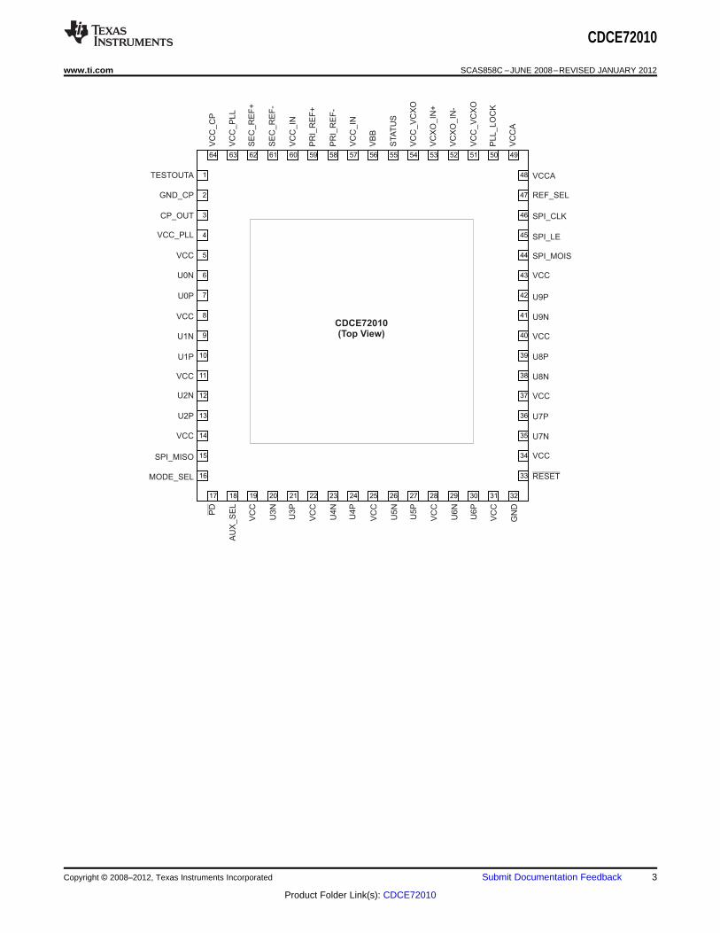
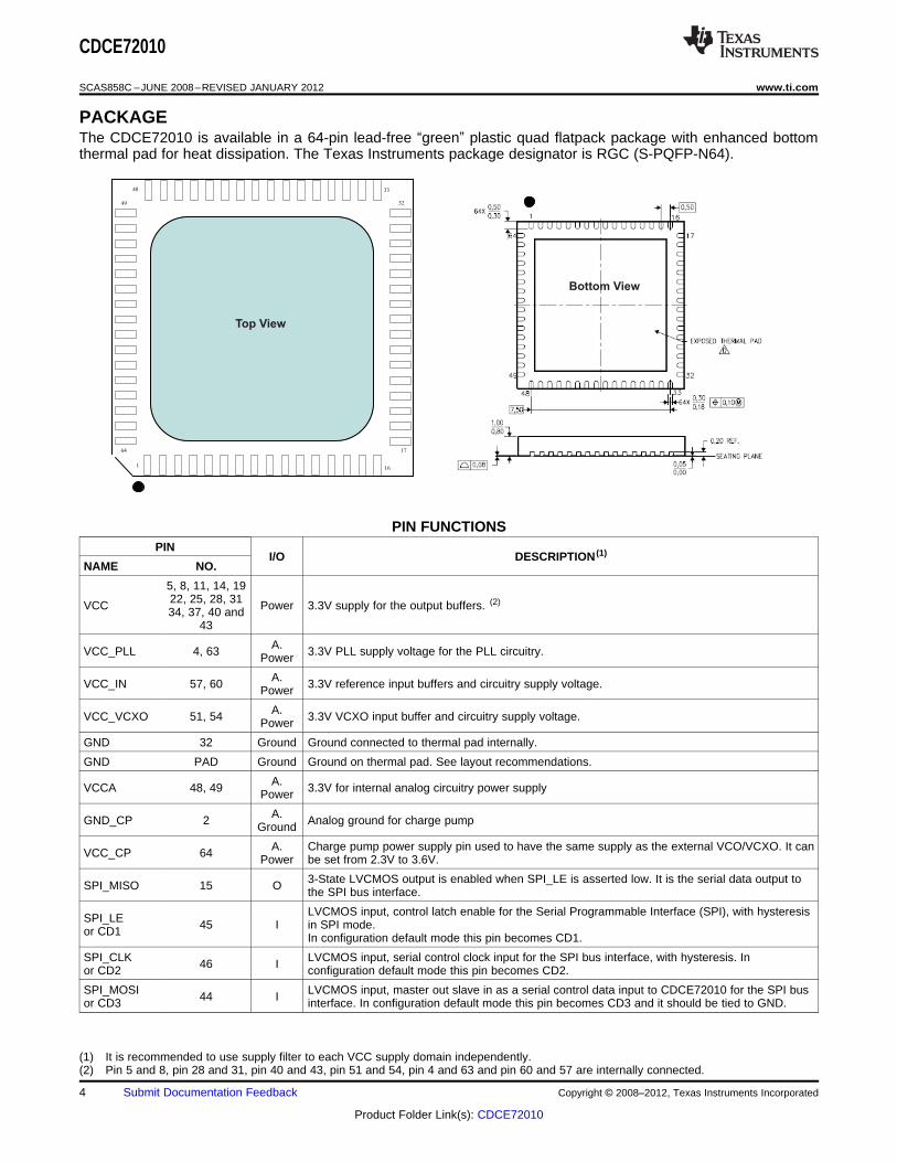
PACKAGEThe CDCE72010 is available in a 64-pin lead-free “green” plastic quad flatpack package with enhanced bottomthermal pad for heat dissipation. The Texas Instruments package designator is RGC (S-PQFP-N64).
PIN FUNCTIONSPIN
I/O DESCRIPTION (1)
NAME NO.
5, 8, 11, 14, 1922, 25, 28, 31VCC Power 3.3V supply for the output buffers. (2)34, 37, 40 and
43
A.VCC_PLL 4, 63 3.3V PLL supply voltage for the PLL circuitry.Power
A.VCC_IN 57, 60 3.3V reference input buffers and circuitry supply voltage.Power
A.VCC_VCXO 51, 54 3.3V VCXO input buffer and circuitry supply voltage.Power
GND 32 Ground Ground connected to thermal pad internally.
GND PAD Ground Ground on thermal pad. See layout recommendations.
A.VCCA 48, 49 3.3V for internal analog circuitry power supplyPower
A.GND_CP 2 Analog ground for charge pumpGround
A. Charge pump power supply pin used to have the same supply as the external VCO/VCXO. It canVCC_CP 64 Power be set from 2.3V to 3.6V.
3-State LVCMOS output is enabled when SPI_LE is asserted low. It is the serial data output toSPI_MISO 15 O the SPI bus interface.
LVCMOS input, control latch enable for the Serial Programmable Interface (SPI), with hysteresisSPI_LE 45 I in SPI mode.or CD1 In configuration default mode this pin becomes CD1.
SPI_CLK LVCMOS input, serial control clock input for the SPI bus interface, with hysteresis. In46 Ior CD2 configuration default mode this pin becomes CD2.
SPI_MOSI LVCMOS input, master out slave in as a serial control data input to CDCE72010 for the SPI bus44 Ior CD3 interface. In configuration default mode this pin becomes CD3 and it should be tied to GND.
(1) It is recommended to use supply filter to each VCC supply domain independently.(2) Pin 5 and 8, pin 28 and 31, pin 40 and 43, pin 51 and 54, pin 4 and 63 and pin 60 and 57 are internally connected.
4 Submit Documentation Feedback Copyright © 2008–2012, Texas Instruments Incorporated
Product Folder Link(s): CDCE72010
CDCE72010
www.ti.com SCAS858C –JUNE 2008–REVISED JANUARY 2012
PIN FUNCTIONS (continued)
PINI/O DESCRIPTION (1)
NAME NO.
SPI MODE = H; when driven high or left unconnected, it defaults to SPI bus interface mode.CD (Configuration Default) MODE = L; If tied low the device goes into configuration defaultMODE_SEL 16 I mode which is configured by CD1, CD2, CD3, and AUX_SEL. In configuration default mode thedevice loads various configuration defaults from the EEPROM into memory at start-up.
This pin is used in CD mode only. If set to “1” or left unconnected, it disables output 9 andenables the AUXILIARY input to drive all outputs from output0 to output8 depending on theAUX_SEL 18 I EEPROM configuration. If driven low in CD mode, it enables output 9 and makes all outputsdriven by the VCXO Input depending on the internal EEPROM configuration.
If Auto Reference Select mode is OFF, this pin acts as an External Input Reference Select Pin;The REF_SEL signal selects one of two input clocks:REF_SEL [1]: PRI_REF is selected;
REF_SEL 47 I REF_SEL [0]: SEC_REF is selected;The input has an internal 150-kΩ pull-up resistor and if left unconnected it will default to logiclevel “1”.If Auto Reference Select mode in ON, this pin not used.
This pin is active low and can be activated externally or by the corresponding bit in the SPIregister (in case of logic high, the SPI setting is valid).
PD 17 I This pin switches the device into powerdown modeThe input has an internal 150-kΩ pull-up resistor and if left unconnected it will default to logiclevel “1”.This LVCMOS input can be programmed (SPI) to act as HOLD or RESET. RESET is the defaultfunction. This pin is active low and can be activated external or via the corresponding bit in theSPI register.In the case of RESET, the CP (Charge Pump) is switched to 3-state and all counters are reset to
RESET or zero. The LVPECL outputs are static low (N) and high (P) respectively, and the LVCMOS33 I outputs are all low or high if inverted. In the case of HOLD, the CP (Charge Pump) is switchedHOLDinto 3-state mode only. After HOLD is released and with the next valid reference clock cycle, thecharge pump is switched back into normal operation (CP stays in 3-state as long as no referenceclock is valid). During HOLD, all outputs are at normal operation. This mode allows externalcontrol of “frequency hold-over” mode. The input has an internal 150-kΩ pull-up resistor.
VCXO_IN+ 53 I VCXO input (+) for LVPECL+, LVDS+, and LVCMOS level inputs.
Complementary VCXO input for LVPECL-, LVDS- inputs. In the case of a LVCMOS level inputVCXO_IN– 52 I on VCXO IN+, ground this pin through 1k resistor.
Universal input buffer (LVPECL, LVDS, LVCMOS) positive input for the Primary ReferencePRI_REF+ 59 I Clock.
Universal input buffer (LVPECL, LVDS) negative input for the Primary Reference Clock. In thePRI_REF– 58 I case of LVCMOS signaling, ground this pin through 1k resistor.
Universal input buffer (LVPECL, LVDS, LVCMOS) positive input for the Secondary ReferenceSEC_REF+ 62 I Clock.
Universal input buffer (LVPECL, LVDS,) negative input for the Secondary Reference Clock. InSEC_REF– 61 I the case of LVCMOS signaling, ground this pin through 1k resistor.
TESTOUTA 1 A Analog Test Point for TI internal testing. Connect a 1kΩ pull-down resistor or leave unconnected.
LVCMOS output for TI internal testing. Leave unconnected unless it is configured as theSTATUS 55 O IREF_CP pin. In this case it should be connected to a 12-kΩ resistor to GND.
CP_OUT 3 AO Charge pump output
VBB 56 AO Internal voltage bias analog output
LVCMOS output for PLL_LOCK information. This pin is set high if the PLL is in lock. This outputPLL_LOCK 50 AO can be programmed to be a digital lock detect or analog lock detect (see description of Analog
Lock).
U0P:U0N 7, 6U1P:U1N 10, 9U2P:U2N 13, 12U3P:U3N 21, 20 The outputs of the CDCE72010 are user definable and can be any combination of up to 9U4P:U4N 24, 23 O LVPECL outputs, 9 LVDS outputs, or up to 18 LVCMOS outputs. The outputs are selectable viaU5P:U5N 27, 26 the SPI interface. The power-up setting is EEPROM configurable.U6P:U6N 30, 29U7P:U7N 36, 35U8P:U8N 39, 38
Copyright © 2008–2012, Texas Instruments Incorporated Submit Documentation Feedback 5
Product Folder Link(s): CDCE72010
CDCE72010
SCAS858C –JUNE 2008–REVISED JANUARY 2012 www.ti.com
PIN FUNCTIONS (continued)
PINI/O DESCRIPTION (1)
NAME NO.
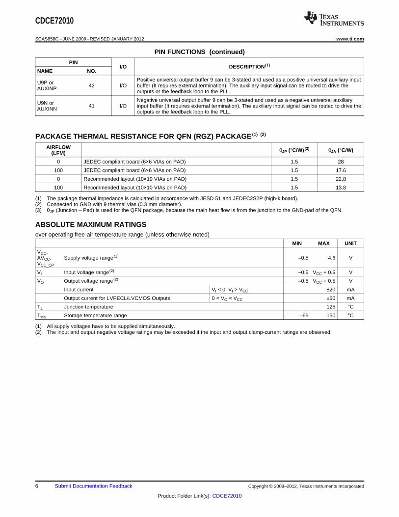
Positive universal output buffer 9 can be 3-stated and used as a positive universal auxiliary inputU9P or 42 I/O buffer (It requires external termination). The auxiliary input signal can be routed to drive theAUXINP outputs or the feedback loop to the PLL.
Negative universal output buffer 9 can be 3-stated and used as a negative universal auxiliaryU9N or 41 I/O input buffer (It requires external termination). The auxiliary input signal can be routed to drive theAUXINN outputs or the feedback loop to the PLL.
PACKAGE THERMAL RESISTANCE FOR QFN (RGZ) PACKAGE (1) (2)
AIRFLOW θJP (°C/W) (3) θJA (°C/W)(LFM)
0 JEDEC compliant board (6×6 VIAs on PAD) 1.5 28
100 JEDEC compliant board (6×6 VIAs on PAD) 1.5 17.6
0 Recommended layout (10×10 VIAs on PAD) 1.5 22.8
100 Recommended layout (10×10 VIAs on PAD) 1.5 13.8
(1) The package thermal impedance is calculated in accordance with JESD 51 and JEDEC2S2P (high-k board).(2) Connected to GND with 9 thermal vias (0.3 mm diameter).(3) θJP (Junction – Pad) is used for the QFN package, because the main heat flow is from the junction to the GND-pad of the QFN.
ABSOLUTE MAXIMUM RATINGSover operating free-air temperature range (unless otherwise noted)
MIN MAX UNIT
VCC,AVCC, Supply voltage range (1) –0.5 4.6 VVCC_CP
VI Input voltage range (2) –0.5 VCC + 0.5 V
VO Output voltage range (2) –0.5 VCC + 0.5 V
Input current VI < 0, VI > VCC ±20 mA
Output current for LVPECL/LVCMOS Outputs 0 < VO < VCC ±50 mA
TJ Junction temperature 125 °CTstg Storage temperature range –65 150 °C
(1) All supply voltages have to be supplied simultaneously.(2) The input and output negative voltage ratings may be exceeded if the input and output clamp-current ratings are observed.
6 Submit Documentation Feedback Copyright © 2008–2012, Texas Instruments Incorporated
Product Folder Link(s): CDCE72010
CDCE72010
www.ti.com SCAS858C –JUNE 2008–REVISED JANUARY 2012
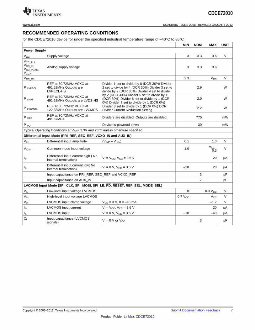
RECOMMENDED OPERATING CONDITIONSfor the CDCE72010 device for under the specified industrial temperature range of –40°C to 85°C
MIN NOM MAX UNIT
Power Supply
VCC Supply voltage 3 3.3 3.6 V
VCC_PLL,VCC_IN, Analog supply voltage 3 3.3 3.6VCC_VCXO,VCCA
VCC_CP 2.3 VCC V
REF at 30.72MHz VCXO at Divider 1 set to divide by 8 (DCR 30%) DividerP LVPECL 491.52MHz Outputs are 2 set to divide by 4 (DCR 30%) Divider 3 set to 2.9 W
LVPECL-HS divide by 2 (DCR 30%) Divider 4 set to divideby 2 (DCR 30%) Divider 5 set to divide by 1REF at 30.72MHz VCXO atP LVDS 2.0 W(DCR 30%) Divider 6 set to divide by 1 (DCR491.52MHz Outputs are LVDS-HS0%) Divider 7 set to divide by 1 (DCR 0%)
REF at 30.72MHz VCXO at Divider 8 set to divide by 1 (DCR 0%) DCR:P LVCMOS 2.2 W122.88MHz Outputs are LVCMOS Divider Current Reduction Setting
REF at 30.72MHz VCXO atP OFF Dividers are disabled. Outputs are disabled. 775 mW491.52MHz
P PD Device is powered down 30 mW
Typical Operating Conditions at VCC= 3.3V and 25°C unless otherwise specified.
Differential Input Mode (PRI_REF, SEC_REF, VCXO_IN and AUX_IN)
VIN Differential input amplitude (VINP – VINN) 0.1 1.3 V
VCC–VICM Common-mode input voltage 1.0 V0.3
Differential input current high ( NoIIH VI = VCC, VCC = 3.6 V 20 μAinternal termination)
Differential input current low( NoIIL VI = 0 V, VCC = 3.6 V –20 20 μAinternal termination)
Input capacitance on PRI_REF, SEC_REF and VCXO_REF 3 pF
Input capacitance on AUX_IN 7 pF
LVCMOS Input Mode (SPI_CLK, SPI_MOSI, SPI_LE, PD, RESET, REF_SEL, MODE_SEL)
VIL Low-level input voltage LVCMOS 0 0.3 VCC V
VIH High-level input voltage LVCMOS 0.7 VCC VCC V
VIK LVCMOS input clamp voltage VCC = 3 V, II = –18 mA –1.2 V
IIH LVCMOS input current VI = VCC, VCC = 3.6 V 20 μA
IIL LVCMOS input VI = 0 V, VCC = 3.6 V –10 –40 μA
CI Input capacitance (LVCMOS VI = 0 V or VCC 3 pFsignals)
Copyright © 2008–2012, Texas Instruments Incorporated Submit Documentation Feedback 7
Product Folder Link(s): CDCE72010
CDCE72010
SCAS858C –JUNE 2008–REVISED JANUARY 2012 www.ti.com
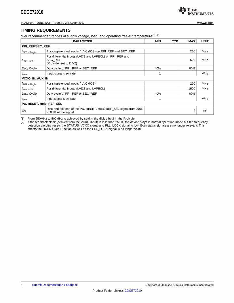
TIMING REQUIREMENTSover recommended ranges of supply voltage, load, and operating free-air temperature (1) (2)
PARAMETER MIN TYP MAX UNIT
PRI_REF/SEC_REF
fREF - Single For single-ended inputs ( LVCMOS) on PRI_REF and SEC_REF 250 MHz
For differential inputs (LVDS and LVPECL) on PRI_REF andfREF - Diff SEC_REF 500 MHz
(R divider set to DIV2)
Duty Cycle Duty cycle of PRI_REF or SEC_REF 40% 60%
tslew Input signal slew rate 1 V/ns
VCXO_IN, AUX_IN
fREF - Single For single-ended inputs ( LVCMOS) 250 MHz
fREF - Diff For differential inputs (LVDS and LVPECL) 1500 MHz
Duty Cycle Duty cycle of PRI_REF or SEC_REF 40% 60%
tslew Input signal slew rate 1 V/ns
PD, RESET, Hold, REF_SEL
Rise and fall time of the PD, RESET, Hold, REF_SEL signal from 20%tr/tf 4 nsto 80% of the signal
(1) From 250MHz to 500MHz is achieved by setting the divide by 2 in the R-divdier(2) If the feedback clock (derived from the VCXO input) is less than 2MHz, the device stays in normal operation mode but the frequency
detection circuitry resets the STATUS_VCXO signal and PLL_LOCK signal to low. Both status signals are no longer relevant. Thisaffects the HOLD-Over-Function as well as the PLL_LOCK signal is no longer valid.
8 Submit Documentation Feedback Copyright © 2008–2012, Texas Instruments Incorporated
Product Folder Link(s): CDCE72010
CDCE72010
www.ti.com SCAS858C –JUNE 2008–REVISED JANUARY 2012
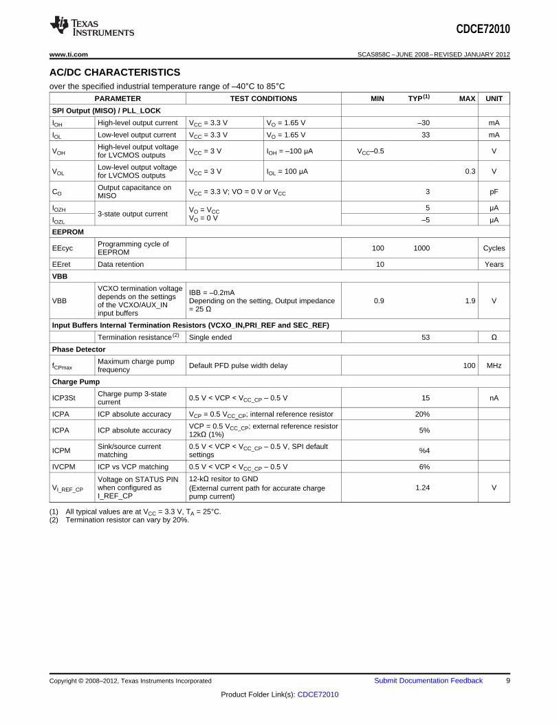
AC/DC CHARACTERISTICSover the specified industrial temperature range of –40°C to 85°C
PARAMETER TEST CONDITIONS MIN TYP (1) MAX UNIT
SPI Output (MISO) / PLL_LOCK
IOH High-level output current VCC = 3.3 V VO = 1.65 V –30 mA
IOL Low-level output current VCC = 3.3 V VO = 1.65 V 33 mA
High-level output voltageVOH VCC = 3 V IOH = –100 μA VCC–0.5 Vfor LVCMOS outputs
Low-level output voltageVOL VCC = 3 V IOL = 100 μA 0.3 Vfor LVCMOS outputs
Output capacitance onCO VCC = 3.3 V; VO = 0 V or VCC 3 pFMISO
IOZH 5 μAVO = VCC3-state output current VO = 0 VIOZL –5 μA
EEPROM
Programming cycle ofEEcyc 100 1000 CyclesEEPROM
EEret Data retention 10 Years
VBB
VCXO termination voltage IBB = –0.2mAdepends on the settingsVBB Depending on the setting, Output impedance 0.9 1.9 Vof the VCXO/AUX_IN = 25 Ωinput buffers
Input Buffers Internal Termination Resistors (VCXO_IN,PRI_REF and SEC_REF)
Termination resistance (2) Single ended 53 ΩPhase Detector
Maximum charge pumpfCPmax Default PFD pulse width delay 100 MHzfrequency
Charge Pump
Charge pump 3-stateICP3St 0.5 V < VCP < VCC_CP – 0.5 V 15 nAcurrent
ICPA ICP absolute accuracy VCP = 0.5 VCC_CP; internal reference resistor 20%
VCP = 0.5 VCC_CP; external reference resistorICPA ICP absolute accuracy 5%12kΩ (1%)
Sink/source current 0.5 V < VCP < VCC_CP – 0.5 V, SPI defaultICPM %4matching settings
IVCPM ICP vs VCP matching 0.5 V < VCP < VCC_CP – 0.5 V 6%
12-kΩ resitor to GNDVoltage on STATUS PINVI_REF_CP when configured as 1.24 V(External current path for accurate charge
I_REF_CP pump current)
(1) All typical values are at VCC = 3.3 V, TA = 25°C.(2) Termination resistor can vary by 20%.
Copyright © 2008–2012, Texas Instruments Incorporated Submit Documentation Feedback 9
Product Folder Link(s): CDCE72010
CDCE72010
SCAS858C –JUNE 2008–REVISED JANUARY 2012 www.ti.com
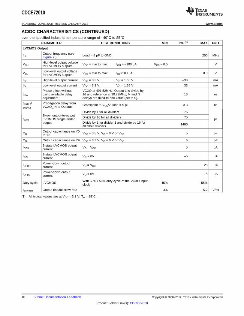
AC/DC CHARACTERISTICS (CONTINUED)over the specified industrial temperature range of –40°C to 85°C
PARAMETER TEST CONDITIONS MIN TYP (1) MAX UNIT
LVCMOS Output
Output frequency (seefclk Load = 5 pF to GND 250 MHzFigure 2 )
High-level output voltageVOH VCC = min to max IOH = –100 μA VCC – 0.5 Vfor LVCMOS outputs
Low-level output voltageVOL VCC = min to max IOL=100 μA 0.3 Vfor LVCMOS outputs
IOH High-level output current VCC = 3.3 V VO = 1.65 V –30 mA
IOL Low-level output current VCC = 3.3 V, VO = 1.65 V 33 mA
Phase offset without VCXO at 491.52MHz, Output 1 is divide bytpho using available delay 16 and reference at 30.72MHz, M and N 13 ns
adjustment delays are fixed to one value (set to 0).
tpd(LH)/ Propagation delay from Crosspoint to VCC/2, load = 5 pF 3.3 nstpd(HL) VCXO_IN to Outputs
Divide by 1 for all dividers 75Skew, output-to-output Divide by 16 for all dividers 75tsk(o) LVCMOS single-ended ps
Divide by 1 for divider 1 and divide by 16 foroutput 1400all other dividers
Output capacitance on Y0CO VCC = 3.3 V; VO = 0 V or VCC 5 pFto Y8
CO Output capacitance on Y9 VCC = 3.3 V; VO = 0 V or VCC 5 pF
3-state LVCMOS outputIOZH VO = VCC 5 μAcurrent
3-state LVCMOS outputIOZL VO = 0V –5 μAcurrent
Power-down outputIOPDH VO = VCC 25 μAcurrent
Power-down outputIOPDL VO = 0V 5 μAcurrent
With 50% / 50% duty cycle of the VCXO inputDuty cycle LVCMOS 45% 55%clock
tslew-rate Output rise/fall slew rate 3.6 5.2 V/ns
(1) All typical values are at VCC = 3.3 V, TA = 25°C.
10 Submit Documentation Feedback Copyright © 2008–2012, Texas Instruments Incorporated
Product Folder Link(s): CDCE72010
CDCE72010
www.ti.com SCAS858C –JUNE 2008–REVISED JANUARY 2012
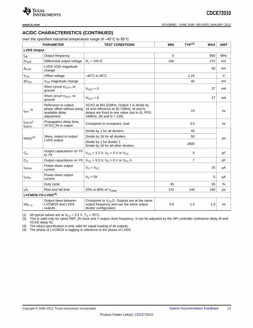
AC/DC CHARACTERISTICS (CONTINUED)over the specified industrial temperature range of –40°C to 85°C
PARAMETER TEST CONDITIONS MIN TYP (1) MAX UNIT
LVDS Output
fclk Output frequency 0 800 MHz
|VOD| Differential output voltage RL = 100 Ω 160 270 mV
LVDS VOD magnitudeΔVOD 50 mVchange
VOS Offset voltage –40°C to 85°C 1.24 V
ΔVOS VOS magnitude change 40 mV
Short circuit VOUT+ to VOUT = 0 27 mAground
Short circuit VOUT– to VOUT = 0 27 mAground
Reference to output VCXO at 491.52MHz, Output 1 is divide byphase offset without using 16 and reference at 30.72MHz, M and Ntpho
(2) 14 nsavailable delay delays are fixed to one value (set to 0), PFD:adjustment 240kHz, (M and N = 128)
tpd(LH)/ Propagation delay time, Crosspoint to crosspoint, load 3.0 nstpd(HL) VCXO_IN to output
Divide by 1 for all dividers 45
Skew, output to output Divide by 16 for all dividers 50tsk(o) (3) psLVDS output Divide by 1 for divider 1 2800Divide by 16 for all other dividers
Output capacitance on Y0CO VCC = 3.3 V; VO = 0 V or VCC 5 pFto Y8
CO Output capacitance on Y9 VCC = 3.3 V; VO = 0 V or VCC 5 7 pF
Power-down outputIOPDH VO = VCC 25 μAcurrent
Power-down outputIOPDL VO = 0V 5 μAcurrent
Duty cycle 45 55 %
tr/tf Rise and fall time 20% to 80% of Voutpp 110 140 160 ps
LVCMOS-TO-LVDS (4)
Output skew between Crosspoint to VCC/2. Outputs are at the sametskP_C LVCMOS and LVDS output frequency and use the same output 0.9 1.4 1.9 ns
outputs divider configuration.
(1) All typical values are at VCC = 3.3 V, TA = 25°C.(2) This is valid only for same REF_IN clock and Y output clock frequency. It can be adjusted by the SPI controller (reference delay M and
VCXO delay N).(3) The tsk(o) specification is only valid for equal loading of all outputs.(4) The phase of LVCMOS is lagging in reference to the phase of LVDS.
Copyright © 2008–2012, Texas Instruments Incorporated Submit Documentation Feedback 11
Product Folder Link(s): CDCE72010
CDCE72010
SCAS858C –JUNE 2008–REVISED JANUARY 2012 www.ti.com
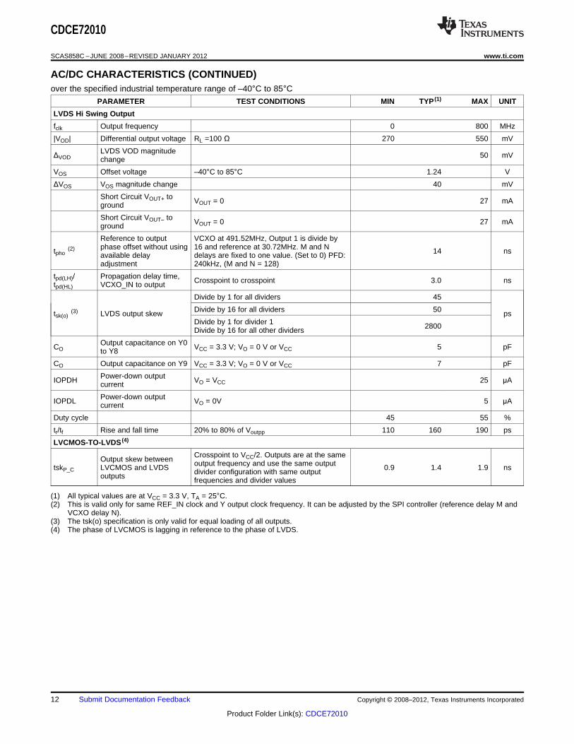
AC/DC CHARACTERISTICS (CONTINUED)over the specified industrial temperature range of –40°C to 85°C
PARAMETER TEST CONDITIONS MIN TYP (1) MAX UNIT
LVDS Hi Swing Output
fclk Output frequency 0 800 MHz
|VOD| Differential output voltage RL =100 Ω 270 550 mV
LVDS VOD magnitudeΔVOD 50 mVchange
VOS Offset voltage –40°C to 85°C 1.24 V
ΔVOS VOS magnitude change 40 mV
Short Circuit VOUT+ to VOUT = 0 27 mAground
Short Circuit VOUT– to VOUT = 0 27 mAground
Reference to output VCXO at 491.52MHz, Output 1 is divide byphase offset without using 16 and reference at 30.72MHz. M and Ntpho
(2) 14 nsavailable delay delays are fixed to one value. (Set to 0) PFD:adjustment 240kHz, (M and N = 128)
tpd(LH)/ Propagation delay time, Crosspoint to crosspoint 3.0 nstpd(HL) VCXO_IN to output
Divide by 1 for all dividers 45
Divide by 16 for all dividers 50tsk(o)(3) LVDS output skew ps
Divide by 1 for divider 1 2800Divide by 16 for all other dividers
Output capacitance on Y0CO VCC = 3.3 V; VO = 0 V or VCC 5 pFto Y8
CO Output capacitance on Y9 VCC = 3.3 V; VO = 0 V or VCC 7 pF
Power-down outputIOPDH VO = VCC 25 μAcurrent
Power-down outputIOPDL VO = 0V 5 μAcurrent
Duty cycle 45 55 %
tr/tf Rise and fall time 20% to 80% of Voutpp 110 160 190 ps
LVCMOS-TO-LVDS (4)
Crosspoint to VCC/2. Outputs are at the sameOutput skew between output frequency and use the same outputtskP_C LVCMOS and LVDS 0.9 1.4 1.9 nsdivider configuration with same outputoutputs frequencies and divider values
(1) All typical values are at VCC = 3.3 V, TA = 25°C.(2) This is valid only for same REF_IN clock and Y output clock frequency. It can be adjusted by the SPI controller (reference delay M and
VCXO delay N).(3) The tsk(o) specification is only valid for equal loading of all outputs.(4) The phase of LVCMOS is lagging in reference to the phase of LVDS.
12 Submit Documentation Feedback Copyright © 2008–2012, Texas Instruments Incorporated
Product Folder Link(s): CDCE72010
CDCE72010
www.ti.com SCAS858C –JUNE 2008–REVISED JANUARY 2012
AC/DC CHARACTERISTICS (CONTINUED)over the specified industrial temperature range of –40°C to 85°C
PARAMETER TEST CONDITIONS MIN TYP (1) MAX UNIT
LVPECL Output
fclk Output frequency 0 1500 MHz
LVPECL high-level outputVOH Load, see Figure 5 VCC – 1.06 VCC – 0.88 Vvoltage
LVPECL low-level outputVOL Load, see Figure 5 VCC – 2.02 VCC – 1.58 Vvoltage
|VOD| Differential output voltage Load, see Figure 5 610 970 mV
Reference to output VCXO at 491.52MHz, Output 1 is divide byphase offset without using 16 and reference at 30.72MHz, M and Ntpho
(2) 14 nsavailable delay delays are fixed to one value (set to 0), PFD:adjustment 240kHz, (M and N = 128)
tpd(LH)/ Propagation delay time, Crosspoint to crosspoint, load 3.4 nstpd(HL) VCXO_IN to output
Divide by 1 for all dividers 45
Divide by 16 for all dividers 50tsk(o)(3) LVPECL output skew ps
Divide by 1 for divider 1 2700Divide by 16 for all other dividers
Output capacitance on Y0CO VCC = 3.3 V; VO = 0 V or VCC 5 pFto Y8
CO Output capacitance on Y9 VCC = 3.3 V; VO = 0 V or VCC 7 pF
Power-down outputIOPDH VO = VCC 25 μAcurrent
Power-down outputIOPDL VO = 0 V 5 μAcurrent
Duty cycle 45 55 %
tr/tf Rise and fall time 20% to 80% of Voutpp 55 75 135 ps
LVDS-TO-LVPECL
Output skew between Crosspoint to Crosspoint with same outputtskP_C LVDS and LVPECL 0.9 1.1 1.3 nsfrequencies and divider valuesoutputs
LVCMOS-TO-LVPECL
Output skew between VCC/2 to Crosspoint; With same outputtskP_C LVCMOS and LVPECL –150 260 700 psfrequencies and divider valuesoutputs
(1) All typical values are at VCC = 3.3 V, TA = 25°C.(2) This is valid only for same REF_IN clock and Y output clock frequency. It can be adjusted by the SPI controller (reference delay M and
VCXO delay N).(3) The tsk(o) specification is only valid for equal loading of all outputs. :
Copyright © 2008–2012, Texas Instruments Incorporated Submit Documentation Feedback 13
Product Folder Link(s): CDCE72010
CDCE72010
SCAS858C –JUNE 2008–REVISED JANUARY 2012 www.ti.com
AC/DC CHARACTERISTICS (CONTINUED)over the specified industrial temperature range of –40°C to 85°C
PARAMETER TEST CONDITIONS MIN TYP (1) MAX UNIT
LVPECL Hi Swing Output
fclk Output frequency 0 1500 MHz
LVPECL high-levelVOH Load, see Figure 5 VCC – 1.11 VCC – 0.87 Voutput voltage
LVPECL low-level outputVOL Load, see Figure 5 VCC – 2.06 VCC – 1.73 Vvoltage
Differential output|VOD| Load, see Figure 5 760 1160 mVvoltage
Reference to output VCXO at 491.52MHz, Output 1 is divide by 16phase offset without and reference at 30.72MHz, M and N delaystpho
(2) 14 nsusing available delay are fixed to one value (set to 0), PFD:adjustment 240kHz, (M and N = 128)
tpd(LH)/ Propagation delay time, Crosspoint to crosspoint, load 3.4 nstpd(HL) VCXO_IN to output
Divide by 1 for all dividers 45
Divide by 16 for all dividers 50tsk(o)(3) LVPECL output skew ps
Divide by 1 for divider 1 2700Divide by 16 for all other dividers
Output capacitance onCO VCC = 3.3 V; VO = 0 V or VCC 5 pFY0 to Y8
Output capacitance onCO VCC = 3.3 V; VO = 0 V or VCC 7 pFY9
Power-down outputIOPDH VO = VCC 25 μAcurrent
Power-down outputIOPDL VO = 0V 5 μAcurrent
Duty cycle 45% 55%
tr/tf Rise and fall time 20% to 80% of Voutpp 55 75 135 ps
LVDS-TO-LVPECL
Output skew between Crosspoint to Crosspoint; with same outputtskP_C LVDS and LVPECL 0.9 1.1 1.3 nsfrequencies and divider valuesoutputs
LVCMOS-TO-LVPECL
Output skew between VCC/2 to Crosspoint; With same outputtskP_C LVCMOS and LVPECL –150 260 700 psfrequencies and divider valuesoutputs (4)
(1) All typical values are at VCC = 3.3 V, TA = 25°C.(2) This is valid only for same REF_IN clock and Y output clock frequency. It can be adjusted by the SPI controller (reference delay M and
VCXO delay N).(3) The tsk(o) specification is only valid for equal loading of all outputs.(4) The phase of LVCMOS is lagging in reference to the phase of LVDS and LVPECL.
14 Submit Documentation Feedback Copyright © 2008–2012, Texas Instruments Incorporated
Product Folder Link(s): CDCE72010
100 W Oscilloscope
5 pfLVCMOS
VCC-2
Oscilloscope
50 W50 W150 W
Oscilloscope
150 W
50 W
50 W
CDCE72010
www.ti.com SCAS858C –JUNE 2008–REVISED JANUARY 2012
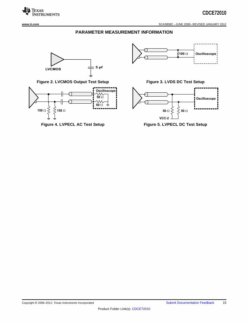
PARAMETER MEASUREMENT INFORMATION
Figure 2. LVCMOS Output Test Setup Figure 3. LVDS DC Test Setup
Figure 4. LVPECL AC Test Setup Figure 5. LVPECL DC Test Setup
Copyright © 2008–2012, Texas Instruments Incorporated Submit Documentation Feedback 15
Product Folder Link(s): CDCE72010
550
600
650
700
750
800
850
900
950
1000
1050
1100
200 400 600 800 1000 1200 1400 1600 1800
(mV)
T = 25 ºCALoad 50 toW
VCC-2C
Frequency - MHz
V = 3.0VCC
V = 3.6VCC
V = 3.3VCC
700
750
800
850
900
950
1000
1050
1100
1150
1200
1250
200 400 600 800 1000 1200 1400 1600 1800
(mV)
T = 25 ºCALoad 50 toW
V – 2VCC
V = 3.0VCC
V = 3.6VCC
V = 3.3VCC
Frequency - MHz
100 200 300 400 500 600 700 800 900100
120
140
160
180
200
220
240
260
280
300
320
(mV)
T = 25 ºCALoad 100 W
V = 3.6VCC
V = 3.0VCC
Frequency - MHz
V = 3.3VCC
0
100
140
180
220
260
300
340
380
420
460
500
100 200 300 400 500 600 700 800 900
(mV)
T = 25 ºCALoad 100 W
Frequency - MHz
V = 3.0VCC
V = 3.3VCC V = 3.6VCC
600
CDCE72010
SCAS858C –JUNE 2008–REVISED JANUARY 2012 www.ti.com
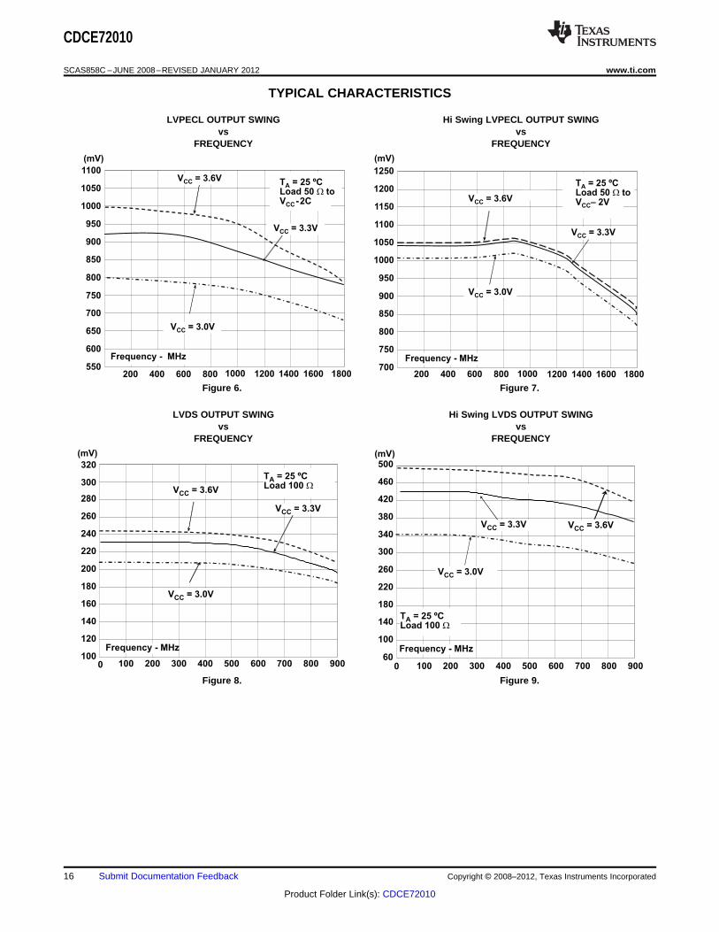
TYPICAL CHARACTERISTICS
LVPECL OUTPUT SWING Hi Swing LVPECL OUTPUT SWINGvs vs
FREQUENCY FREQUENCY
Figure 6. Figure 7.
LVDS OUTPUT SWING Hi Swing LVDS OUTPUT SWINGvs vs
FREQUENCY FREQUENCY
Figure 8. Figure 9.
16 Submit Documentation Feedback Copyright © 2008–2012, Texas Instruments Incorporated
Product Folder Link(s): CDCE72010
1.8
2.0
2.2
2.4
2.6
2.8
3.0
3.2
3.4
3.6
3.8
4.0
100 200 300 400 500
V = 3.3VCC
VC C = 3.6V
V = 3.0VCC
T = 25 ºCALoad 5pF
(V)
Frequency - MHz
CDCE72010
www.ti.com SCAS858C –JUNE 2008–REVISED JANUARY 2012
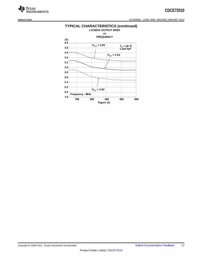
TYPICAL CHARACTERISTICS (continued)LVCMOS OUTPUT WING
vsFREQUENCY
Figure 10.
Copyright © 2008–2012, Texas Instruments Incorporated Submit Documentation Feedback 17
Product Folder Link(s): CDCE72010
CDCE72010
SCAS858C –JUNE 2008–REVISED JANUARY 2012 www.ti.com
APPLICATION INFORMATION
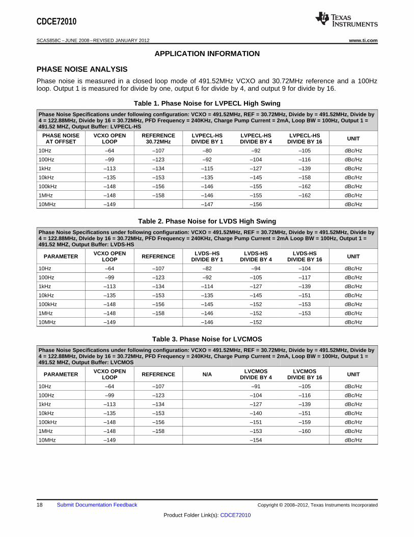
PHASE NOISE ANALYSIS
Phase noise is measured in a closed loop mode of 491.52MHz VCXO and 30.72MHz reference and a 100Hzloop. Output 1 is measured for divide by one, output 6 for divide by 4, and output 9 for divide by 16.
Table 1. Phase Noise for LVPECL High Swing
Phase Noise Specifications under following configuration: VCXO = 491.52MHz, REF = 30.72MHz, Divide by = 491.52MHz, Divide by4 = 122.88MHz, Divide by 16 = 30.72MHz, PFD Frequency = 240KHz, Charge Pump Current = 2mA, Loop BW = 100Hz, Output 1 =491.52 MHZ, Output Buffer: LVPECL-HS
PHASE NOISE VCXO OPEN REFERENCE LVPECL-HS LVPECL-HS LVPECL-HS UNITAT OFFSET LOOP 30.72MHz DIVIDE BY 1 DIVIDE BY 4 DIVIDE BY 16
10Hz –64 –107 –80 –92 –105 dBc/Hz
100Hz –99 –123 –92 –104 –116 dBc/Hz
1kHz –113 –134 –115 –127 –139 dBc/Hz
10kHz –135 –153 –135 –145 –158 dBc/Hz
100kHz –148 –156 –146 –155 –162 dBc/Hz
1MHz –148 –158 –146 –155 –162 dBc/Hz
10MHz –149 –147 –156 dBc/Hz
Table 2. Phase Noise for LVDS High Swing
Phase Noise Specifications under following configuration: VCXO = 491.52MHz, REF = 30.72MHz, Divide by = 491.52MHz, Divide by4 = 122.88MHz, DIvide by 16 = 30.72MHz, PFD Frequency = 240KHz, Charge Pump Current = 2mA Loop BW = 100Hz, Output 1 =491.52 MHZ, Output Buffer: LVDS-HS
VCXO OPEN LVDS–HS LVDS-HS LVDS-HSPARAMETER REFERENCE UNITLOOP DIVIDE BY 1 DIVIDE BY 4 DIVIDE BY 16
10Hz –64 –107 –82 –94 –104 dBc/Hz
100Hz –99 –123 –92 –105 –117 dBc/Hz
1kHz –113 –134 –114 –127 –139 dBc/Hz
10kHz –135 –153 –135 –145 –151 dBc/Hz
100kHz –148 –156 –145 –152 –153 dBc/Hz
1MHz –148 –158 –146 –152 –153 dBc/Hz
10MHz –149 –146 –152 dBc/Hz
Table 3. Phase Noise for LVCMOS
Phase Noise Specifications under following configuration: VCXO = 491.52MHz, REF = 30.72MHz, Divide by = 491.52MHz, Divide by4 = 122.88MHz, DIvide by 16 = 30.72MHz, PFD Frequency = 240KHz, Charge Pump Current = 2mA, Loop BW = 100Hz, Output 1 =491.52 MHZ, Output Buffer: LVCMOS
VCXO OPEN LVCMOS LVCMOSPARAMETER REFERENCE N/A UNITLOOP DIVIDE BY 4 DIVIDE BY 16
10Hz –64 –107 –91 –105 dBc/Hz
100Hz –99 –123 –104 –116 dBc/Hz
1kHz –113 –134 –127 –139 dBc/Hz
10kHz –135 –153 –140 –151 dBc/Hz
100kHz –148 –156 –151 –159 dBc/Hz
1MHz –148 –158 –153 –160 dBc/Hz
10MHz –149 –154 dBc/Hz
18 Submit Documentation Feedback Copyright © 2008–2012, Texas Instruments Incorporated
Product Folder Link(s): CDCE72010
0123456789101112131415161718192021222324252627 0123
0123456789101112131415161718192021222324252627 0123
Address
Bits
(4)
Last in /
Last out
First In /
First Out
SPI_LE
SPI_CLK
SPI_MOSI
SPI_MISOSPI_LE
SPI_CLK
SPI_MOSI
SPI_MISO
SPI Master (Host)
SPI_LE
SPI_CLK
SPI_MOSI
SPI_MISO
SPI Slave (CDCE62005)
Device Register N
0123456789101112131415161718192021222324252627
SPI Register
Data Bits (28)
CDCE72010
www.ti.com SCAS858C –JUNE 2008–REVISED JANUARY 2012
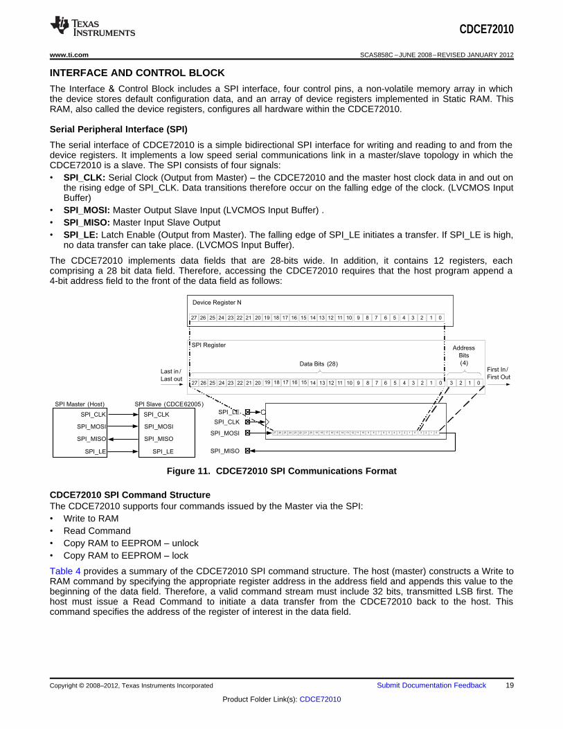
INTERFACE AND CONTROL BLOCK
The Interface & Control Block includes a SPI interface, four control pins, a non-volatile memory array in whichthe device stores default configuration data, and an array of device registers implemented in Static RAM. ThisRAM, also called the device registers, configures all hardware within the CDCE72010.
Serial Peripheral Interface (SPI)
The serial interface of CDCE72010 is a simple bidirectional SPI interface for writing and reading to and from thedevice registers. It implements a low speed serial communications link in a master/slave topology in which theCDCE72010 is a slave. The SPI consists of four signals:• SPI_CLK: Serial Clock (Output from Master) – the CDCE72010 and the master host clock data in and out on
the rising edge of SPI_CLK. Data transitions therefore occur on the falling edge of the clock. (LVCMOS InputBuffer)
• SPI_MOSI: Master Output Slave Input (LVCMOS Input Buffer) .• SPI_MISO: Master Input Slave Output• SPI_LE: Latch Enable (Output from Master). The falling edge of SPI_LE initiates a transfer. If SPI_LE is high,
no data transfer can take place. (LVCMOS Input Buffer).
The CDCE72010 implements data fields that are 28-bits wide. In addition, it contains 12 registers, eachcomprising a 28 bit data field. Therefore, accessing the CDCE72010 requires that the host program append a4-bit address field to the front of the data field as follows:
Figure 11. CDCE72010 SPI Communications Format
CDCE72010 SPI Command StructureThe CDCE72010 supports four commands issued by the Master via the SPI:• Write to RAM• Read Command• Copy RAM to EEPROM – unlock• Copy RAM to EEPROM – lock
Table 4 provides a summary of the CDCE72010 SPI command structure. The host (master) constructs a Write toRAM command by specifying the appropriate register address in the address field and appends this value to thebeginning of the data field. Therefore, a valid command stream must include 32 bits, transmitted LSB first. Thehost must issue a Read Command to initiate a data transfer from the CDCE72010 back to the host. Thiscommand specifies the address of the register of interest in the data field.
Copyright © 2008–2012, Texas Instruments Incorporated Submit Documentation Feedback 19
Product Folder Link(s): CDCE72010
SPI_CLK
SPI_MOSI
SPI_LE
SPI_MISO
SPI_LE
SPI_CLK
SPI_MOSI
SPI_MISO
SPI _CLK
SPI _MOSI
SPI _MISO
SPI _LE
CDCE72010
SCAS858C –JUNE 2008–REVISED JANUARY 2012 www.ti.com
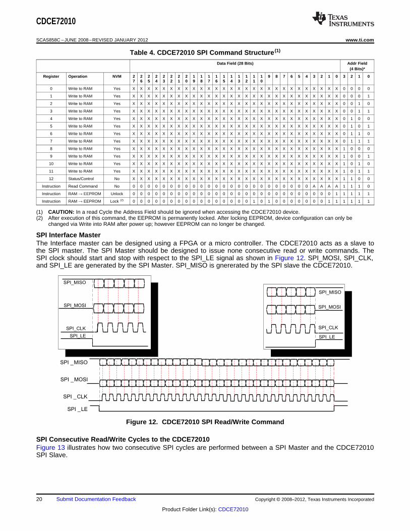
Table 4. CDCE72010 SPI Command Structure (1)
Data Field (28 Bits) Addr Field(4 Bits)*
Register Operation NVM 2 2 2 2 2 2 2 2 1 1 1 1 1 1 1 1 1 1 9 8 7 6 5 4 3 2 1 0 3 2 1 07 6 5 4 3 2 1 0 9 8 7 6 5 4 3 2 1 0
0 Write to RAM Yes X X X X X X X X X X X X X X X X X X X X X X X X X X X X 0 0 0 0
1 Write to RAM Yes X X X X X X X X X X X X X X X X X X X X X X X X X X X X 0 0 0 1
2 Write to RAM Yes X X X X X X X X X X X X X X X X X X X X X X X X X X X X 0 0 1 0
3 Write to RAM Yes X X X X X X X X X X X X X X X X X X X X X X X X X X X X 0 0 1 1
4 Write to RAM Yes X X X X X X X X X X X X X X X X X X X X X X X X X X X X 0 1 0 0
5 Write to RAM Yes X X X X X X X X X X X X X X X X X X X X X X X X X X X X 0 1 0 1
6 Write to RAM Yes X X X X X X X X X X X X X X X X X X X X X X X X X X X X 0 1 1 0
7 Write to RAM Yes X X X X X X X X X X X X X X X X X X X X X X X X X X X X 0 1 1 1
8 Write to RAM Yes X X X X X X X X X X X X X X X X X X X X X X X X X X X X 1 0 0 0
9 Write to RAM Yes X X X X X X X X X X X X X X X X X X X X X X X X X X X X 1 0 0 1
10 Write to RAM Yes X X X X X X X X X X X X X X X X X X X X X X X X X X X X 1 0 1 0
11 Write to RAM Yes X X X X X X X X X X X X X X X X X X X X X X X X X X X X 1 0 1 1
12 Status/Control No X X X X X X X X X X X X X X X X X X X X X X X X X X X X 1 1 0 0
Instruction Read Command No 0 0 0 0 0 0 0 0 0 0 0 0 0 0 0 0 0 0 0 0 0 0 0 0 A A A A 1 1 1 0
Instruction RAM → EEPROM Unlock 0 0 0 0 0 0 0 0 0 0 0 0 0 0 0 0 0 0 0 0 0 0 0 0 0 0 0 1 1 1 1 1
Instruction RAM → EEPROM Lock (2) 0 0 0 0 0 0 0 0 0 0 0 0 0 0 0 0 1 0 1 0 0 0 0 0 0 0 1 1 1 1 1 1
(1) CAUTION: In a read Cycle the Address Field should be ignored when accessing the CDCE72010 device.(2) After execution of this command, the EEPROM is permanently locked. After locking EEPROM, device configuration can only be
changed via Write into RAM after power up; however EEPROM can no longer be changed.
SPI Interface MasterThe Interface master can be designed using a FPGA or a micro controller. The CDCE72010 acts as a slave tothe SPI master. The SPI Master should be designed to issue none consecutive read or write commands. TheSPI clock should start and stop with respect to the SPI_LE signal as shown in Figure 12. SPI_MOSI, SPI_CLK,and SPI_LE are generated by the SPI Master. SPI_MISO is gnererated by the SPI slave the CDCE72010.
Figure 12. CDCE72010 SPI Read/Write Command
SPI Consecutive Read/Write Cycles to the CDCE72010Figure 13 illustrates how two consecutive SPI cycles are performed between a SPI Master and the CDCE72010SPI Slave.
20 Submit Documentation Feedback Copyright © 2008–2012, Texas Instruments Incorporated
Product Folder Link(s): CDCE72010
SPI_CLK
SPI_MOSI
SPI_MISO
SPI_LE
SPI MasterSPI Slave
Bit 0 Bit 1 Bit 29 Bit 30 Bit 31SPI _MOSI
SPI _CLK
SPI _LE
SPI_CLK
SPI_MOSI
SPI_MISO
SPI_LE
Bit30 Bit31
Bit0=0 Bit1
CDCE72010
www.ti.com SCAS858C –JUNE 2008–REVISED JANUARY 2012
Figure 13. Consecutive Read/Write Cycles
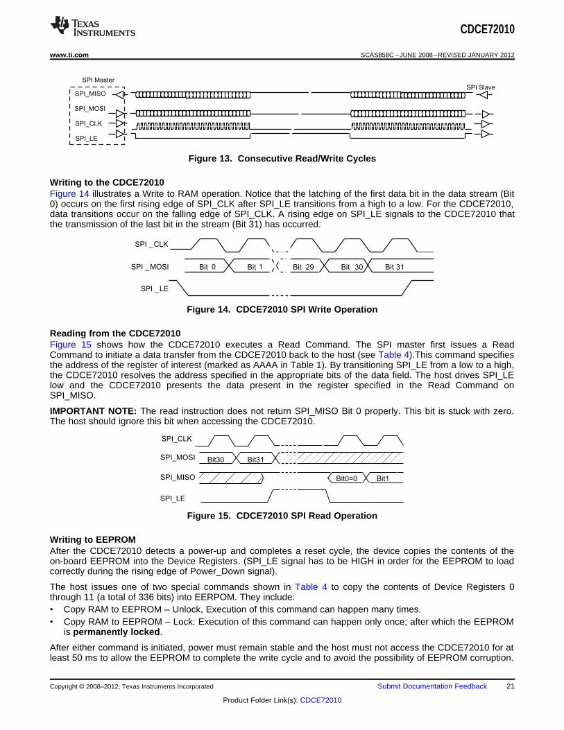
Writing to the CDCE72010Figure 14 illustrates a Write to RAM operation. Notice that the latching of the first data bit in the data stream (Bit0) occurs on the first rising edge of SPI_CLK after SPI_LE transitions from a high to a low. For the CDCE72010,data transitions occur on the falling edge of SPI_CLK. A rising edge on SPI_LE signals to the CDCE72010 thatthe transmission of the last bit in the stream (Bit 31) has occurred.
Figure 14. CDCE72010 SPI Write Operation
Reading from the CDCE72010Figure 15 shows how the CDCE72010 executes a Read Command. The SPI master first issues a ReadCommand to initiate a data transfer from the CDCE72010 back to the host (see Table 4).This command specifiesthe address of the register of interest (marked as AAAA in Table 1). By transitioning SPI_LE from a low to a high,the CDCE72010 resolves the address specified in the appropriate bits of the data field. The host drives SPI_LElow and the CDCE72010 presents the data present in the register specified in the Read Command onSPI_MISO.
IMPORTANT NOTE: The read instruction does not return SPI_MISO Bit 0 properly. This bit is stuck with zero.The host should ignore this bit when accessing the CDCE72010.
Figure 15. CDCE72010 SPI Read Operation
Writing to EEPROMAfter the CDCE72010 detects a power-up and completes a reset cycle, the device copies the contents of theon-board EEPROM into the Device Registers. (SPI_LE signal has to be HIGH in order for the EEPROM to loadcorrectly during the rising edge of Power_Down signal).
The host issues one of two special commands shown in Table 4 to copy the contents of Device Registers 0through 11 (a total of 336 bits) into EERPOM. They include:• Copy RAM to EEPROM – Unlock, Execution of this command can happen many times.• Copy RAM to EEPROM – Lock: Execution of this command can happen only once; after which the EEPROM
is permanently locked.
After either command is initiated, power must remain stable and the host must not access the CDCE72010 for atleast 50 ms to allow the EEPROM to complete the write cycle and to avoid the possibility of EEPROM corruption.
Copyright © 2008–2012, Texas Instruments Incorporated Submit Documentation Feedback 21
Product Folder Link(s): CDCE72010
Bit0 Bit1 Bit30Bit29
t1
t2 t3
t4 t5
t6
t7
Bit31
SPI_CLK
SPI_MOSI
SPI_LE
Bit30
Bit0 = 0 Bit1 Bit2
Bit31
t2 t3
t4 t5
t8
t7
t6 t9
SPI_CLK
SPI_MOSI
SPI_MISO
SPI_LE
CDCE72010
SCAS858C –JUNE 2008–REVISED JANUARY 2012 www.ti.com
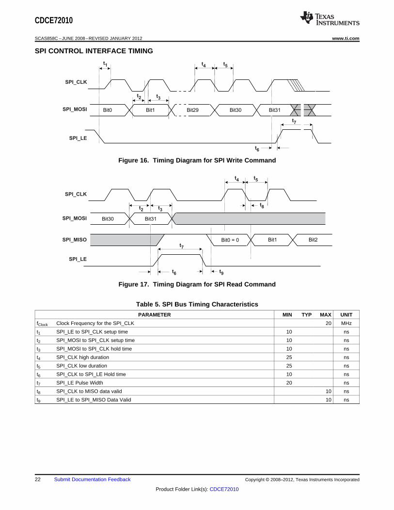
SPI CONTROL INTERFACE TIMING
Figure 16. Timing Diagram for SPI Write Command
Figure 17. Timing Diagram for SPI Read Command
Table 5. SPI Bus Timing Characteristics
PARAMETER MIN TYP MAX UNIT
fClock Clock Frequency for the SPI_CLK 20 MHz
t1 SPI_LE to SPI_CLK setup time 10 ns
t2 SPI_MOSI to SPI_CLK setup time 10 ns
t3 SPI_MOSI to SPI_CLK hold time 10 ns
t4 SPI_CLK high duration 25 ns
t5 SPI_CLK low duration 25 ns
t6 SPI_CLK to SPI_LE Hold time 10 ns
t7 SPI_LE Pulse Width 20 ns
t8 SPI_CLK to MISO data valid 10 ns
t9 SPI_LE to SPI_MISO Data Valid 10 ns
22 Submit Documentation Feedback Copyright © 2008–2012, Texas Instruments Incorporated
Product Folder Link(s): CDCE72010
CDCE72010
www.ti.com SCAS858C –JUNE 2008–REVISED JANUARY 2012
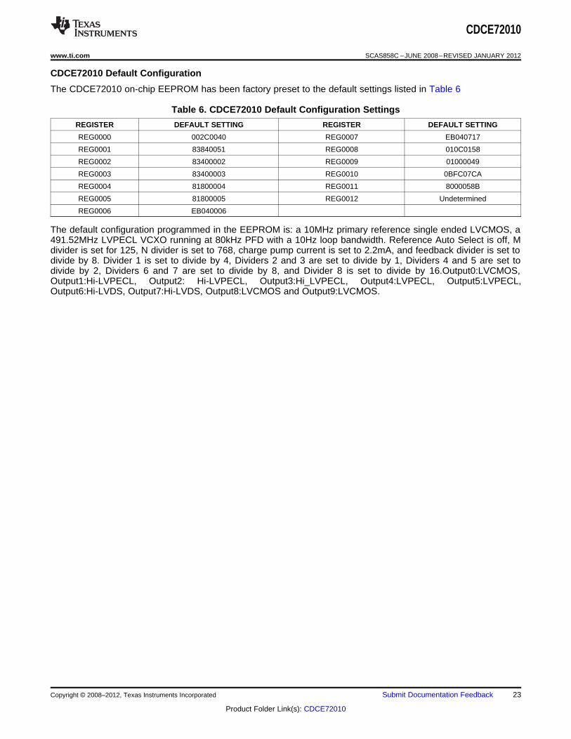
CDCE72010 Default Configuration
The CDCE72010 on-chip EEPROM has been factory preset to the default settings listed in Table 6
Table 6. CDCE72010 Default Configuration Settings
REGISTER DEFAULT SETTING REGISTER DEFAULT SETTING
REG0000 002C0040 REG0007 EB040717
REG0001 83840051 REG0008 010C0158
REG0002 83400002 REG0009 01000049
REG0003 83400003 REG0010 0BFC07CA
REG0004 81800004 REG0011 8000058B
REG0005 81800005 REG0012 Undetermined
REG0006 EB040006
The default configuration programmed in the EEPROM is: a 10MHz primary reference single ended LVCMOS, a491.52MHz LVPECL VCXO running at 80kHz PFD with a 10Hz loop bandwidth. Reference Auto Select is off, Mdivider is set for 125, N divider is set to 768, charge pump current is set to 2.2mA, and feedback divider is set todivide by 8. Divider 1 is set to divide by 4, Dividers 2 and 3 are set to divide by 1, Dividers 4 and 5 are set todivide by 2, Dividers 6 and 7 are set to divide by 8, and Divider 8 is set to divide by 16.Output0:LVCMOS,Output1:Hi-LVPECL, Output2: Hi-LVPECL, Output3:Hi_LVPECL, Output4:LVPECL, Output5:LVPECL,Output6:Hi-LVDS, Output7:Hi-LVDS, Output8:LVCMOS and Output9:LVCMOS.
Copyright © 2008–2012, Texas Instruments Incorporated Submit Documentation Feedback 23
Product Folder Link(s): CDCE72010
CDCE72010
SCAS858C –JUNE 2008–REVISED JANUARY 2012 www.ti.com
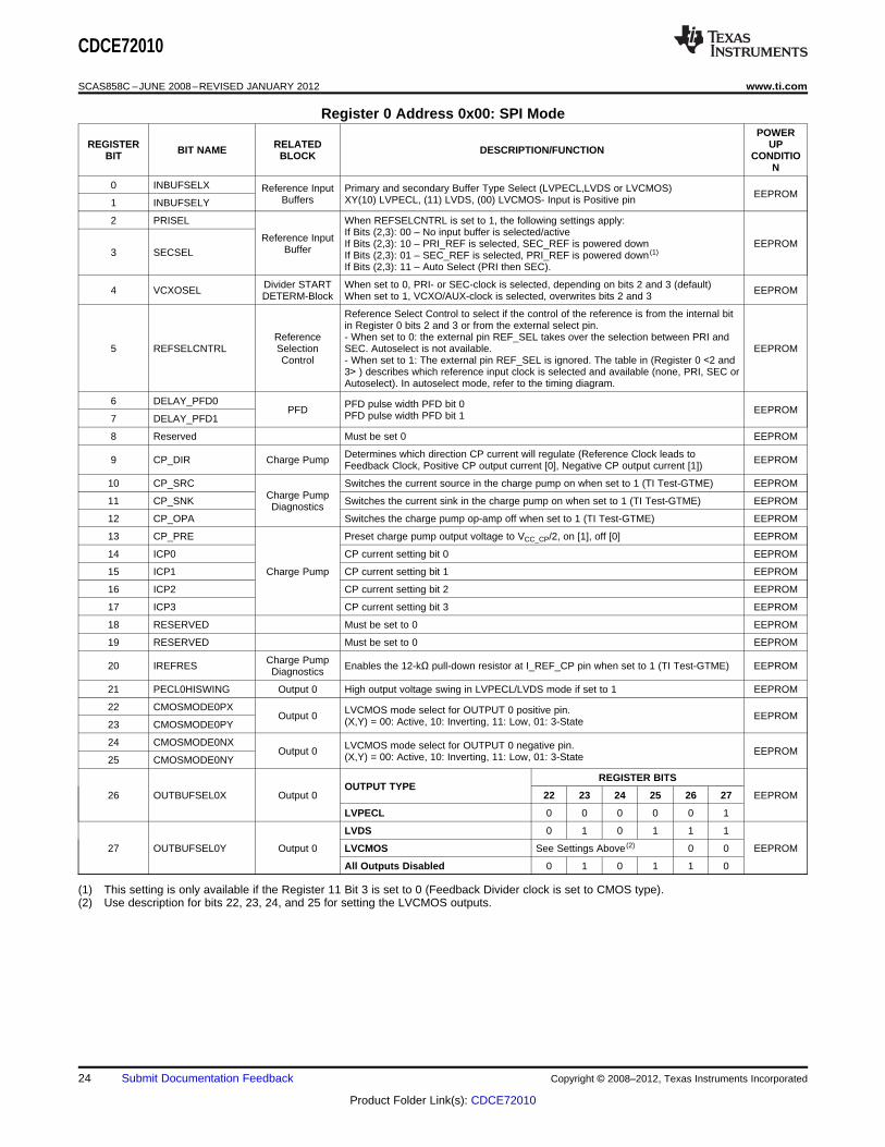
Register 0 Address 0x00: SPI ModePOWER
REGISTER RELATED UPBIT NAME DESCRIPTION/FUNCTIONBIT BLOCK CONDITION
0 INBUFSELX Reference Input Primary and secondary Buffer Type Select (LVPECL,LVDS or LVCMOS) EEPROMBuffers XY(10) LVPECL, (11) LVDS, (00) LVCMOS- Input is Positive pin1 INBUFSELY
2 PRISEL When REFSELCNTRL is set to 1, the following settings apply:If Bits (2,3): 00 – No input buffer is selected/activeReference Input If Bits (2,3): 10 – PRI_REF is selected, SEC_REF is powered down EEPROMBuffer3 SECSEL If Bits (2,3): 01 – SEC_REF is selected, PRI_REF is powered down (1)
If Bits (2,3): 11 – Auto Select (PRI then SEC).
Divider START When set to 0, PRI- or SEC-clock is selected, depending on bits 2 and 3 (default)4 VCXOSEL EEPROMDETERM-Block When set to 1, VCXO/AUX-clock is selected, overwrites bits 2 and 3
Reference Select Control to select if the control of the reference is from the internal bitin Register 0 bits 2 and 3 or from the external select pin.
Reference - When set to 0: the external pin REF_SEL takes over the selection between PRI and5 REFSELCNTRL Selection SEC. Autoselect is not available. EEPROM
Control - When set to 1: The external pin REF_SEL is ignored. The table in (Register 0 <2 and3> ) describes which reference input clock is selected and available (none, PRI, SEC orAutoselect). In autoselect mode, refer to the timing diagram.
6 DELAY_PFD0 PFD pulse width PFD bit 0PFD EEPROMPFD pulse width PFD bit 17 DELAY_PFD1
8 Reserved Must be set 0 EEPROM
Determines which direction CP current will regulate (Reference Clock leads to9 CP_DIR Charge Pump EEPROMFeedback Clock, Positive CP output current [0], Negative CP output current [1])
10 CP_SRC Switches the current source in the charge pump on when set to 1 (TI Test-GTME) EEPROMCharge Pump11 CP_SNK Switches the current sink in the charge pump on when set to 1 (TI Test-GTME) EEPROMDiagnostics
12 CP_OPA Switches the charge pump op-amp off when set to 1 (TI Test-GTME) EEPROM
13 CP_PRE Preset charge pump output voltage to VCC_CP/2, on [1], off [0] EEPROM
14 ICP0 CP current setting bit 0 EEPROM
15 ICP1 Charge Pump CP current setting bit 1 EEPROM
16 ICP2 CP current setting bit 2 EEPROM
17 ICP3 CP current setting bit 3 EEPROM
18 RESERVED Must be set to 0 EEPROM
19 RESERVED Must be set to 0 EEPROM
Charge Pump20 IREFRES Enables the 12-kΩ pull-down resistor at I_REF_CP pin when set to 1 (TI Test-GTME) EEPROMDiagnostics
21 PECL0HISWING Output 0 High output voltage swing in LVPECL/LVDS mode if set to 1 EEPROM
22 CMOSMODE0PX LVCMOS mode select for OUTPUT 0 positive pin.Output 0 EEPROM(X,Y) = 00: Active, 10: Inverting, 11: Low, 01: 3-State23 CMOSMODE0PY
24 CMOSMODE0NX LVCMOS mode select for OUTPUT 0 negative pin.Output 0 EEPROM(X,Y) = 00: Active, 10: Inverting, 11: Low, 01: 3-State25 CMOSMODE0NY
REGISTER BITSOUTPUT TYPE
26 OUTBUFSEL0X Output 0 22 23 24 25 26 27 EEPROM
LVPECL 0 0 0 0 0 1
LVDS 0 1 0 1 1 1
27 OUTBUFSEL0Y Output 0 LVCMOS See Settings Above (2) 0 0 EEPROM
All Outputs Disabled 0 1 0 1 1 0
(1) This setting is only available if the Register 11 Bit 3 is set to 0 (Feedback Divider clock is set to CMOS type).(2) Use description for bits 22, 23, 24, and 25 for setting the LVCMOS outputs.
24 Submit Documentation Feedback Copyright © 2008–2012, Texas Instruments Incorporated
Product Folder Link(s): CDCE72010
CDCE72010
www.ti.com SCAS858C –JUNE 2008–REVISED JANUARY 2012
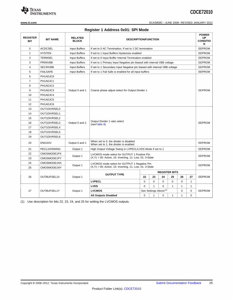
Register 1 Address 0x01: SPI ModePOWER
REGISTER RELATED UPBIT NAME DESCRIPTION/FUNCTIONBLOCK CONDITIOBITN
0 ACDCSEL Input Buffers If set to 0 AC Termination, If set to 1 DC termination EEPROM
1 HYSTEN Input Buffers If set to 1 Input Buffers Hysteresis enabled EEPROM
2 TERMSEL Input Buffers If set to 0 Input Buffer Internal Termination enabled EEPROM
3 PRIINVBB Input Buffers If set to 1 Primary Input Negative pin biased with internal VBB voltage EEPROM
4 SECINVBB Input Buffers If set to 1 Secondary Input Negative pin biased with internal VBB voltage EEPROM
5 FAILSAFE Input Buffers If set to 1 Fail Safe is enabled for all input buffers EEPROM
6 PH1ADJC0
7 PH1ADJC1
8 PH1ADJC2
9 PH1ADJC3 Output 0 and 1 Coarse phase adjust select for Output Divider 1 EEPROM
10 PH1ADJC4
11 PH1ADJC5
12 PH1ADJC6
13 OUT1DIVRSEL0
14 OUT1DIVRSEL1
15 OUT1DIVRSEL2Output Divider 1 ratio select16 OUT1DIVRSEL3 Output 0 and 1 EEPROM(seeTable 8)
17 OUT1DIVRSEL4
18 OUT1DIVRSEL5
19 OUT1DIVRSEL6
When set to 0, the divider is disabled20 EN01DIV Output 0 and 1 EEPROMWhen set to 1, the divider is enabled
21 PECL1HISWING Output 1 High Output Voltage Swing in LVPECL/LVDS Mode if set to 1 EEPROM
22 CMOSMODE1PX LVCMOS mode select for OUTPUT 1 Positive Pin.Output 1 EEPROM(X,Y) = 00: Active, 10: Inverting, 11: Low, 01: 3-State23 CMOSMODE1PY
24 CMOSMODE1NX LVCMOS mode select for OUTPUT 1 Negative Pin.Output 1 EEPROM(X,Y) = 00: Active, 10: Inverting, 11: Low, 01: 3-State25 CMOSMODE1NY
REGISTER BITSOUTPUT TYPE
26 OUTBUFSEL1X Output 1 22 23 24 25 26 27 EEPROM
LVPECL 0 0 0 0 0 1
LVDS 0 1 0 1 1 1
27 OUTBUFSEL1Y Output 1 LVCMOS See Settings Above (1) 0 0 EEPROM
All Outputs Disabled 0 1 0 1 1 0
(1) Use description for bits 22, 23, 24, and 25 for setting the LVCMOS outputs.
Copyright © 2008–2012, Texas Instruments Incorporated Submit Documentation Feedback 25
Product Folder Link(s): CDCE72010
CDCE72010
SCAS858C –JUNE 2008–REVISED JANUARY 2012 www.ti.com
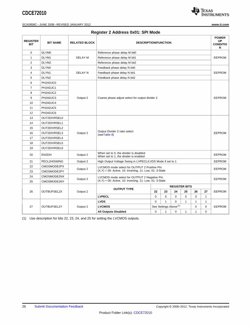
Register 2 Address 0x01: SPI ModePOWER
REGISTER UPBIT NAME RELATED BLOCK DESCRIPTION/FUNCTIONBIT CONDITION
0 DLYM0 Reference phase delay M bit0
1 DLYM1 DELAY M Reference phase delay M bit1 EEPROM
2 DLYM2 Reference phase delay M bit2
3 DLYN0 Feedback phase delay N bit0
4 DLYN1 DELAY N Feedback phase delay N bit1 EEPROM
5 DLYN2 Feedback phase delay N bit2
6 PH2ADJC0
7 PH2ADJC1
8 PH2ADJC2
9 PH2ADJC3 Output 2 Coarse phase adjust select for output divider 2 EEPROM
10 PH2ADJC4
11 PH2ADJC5
12 PH2ADJC6
13 OUT2DIVRSEL0
14 OUT2DIVRSEL1
15 OUT2DIVRSEL2Output Divider 2 ratio select16 OUT2DIVRSEL3 Output 2 EEPROM(seeTable 8)
17 OUT2DIVRSEL4
18 OUT2DIVRSEL5
19 OUT2DIVRSEL6
When set to 0, the divider is disabled20 EN2DIV Output 2 EEPROMWhen set to 1, the divider is enabled
21 PECL2HISWING Output 2 High Output Voltage Swing in LVPECL/LVDS Mode if set to 1 EEPROM
22 CMOSMODE2PX LVCMOS mode select for OUTPUT 2 Positive Pin.Output 2 EEPROM(X,Y) = 00: Active, 10: Inverting, 11: Low, 01: 3-State23 CMOSMODE2PY
24 CMOSMODE2NX LVCMOS mode select for OUTPUT 2 Negative Pin.Output 2 EEPROM(X,Y) = 00: Active, 10: Inverting, 11: Low, 01: 3-State25 CMOSMODE2NY
REGISTER BITSOUTPUT TYPE
26 OUTBUFSEL2X Output 2 22 23 24 25 26 27 EEPROM
LVPECL 0 0 0 0 0 1
LVDS 0 1 0 1 1 1
27 OUTBUFSEL2Y Output 2 LVCMOS See Settings Above (1) 0 0 EEPROM
All Outputs Disabled 0 1 0 1 1 0
(1) Use description for bits 22, 23, 24, and 25 for setting the LVCMOS outputs.
26 Submit Documentation Feedback Copyright © 2008–2012, Texas Instruments Incorporated
Product Folder Link(s): CDCE72010
CDCE72010
www.ti.com SCAS858C –JUNE 2008–REVISED JANUARY 2012
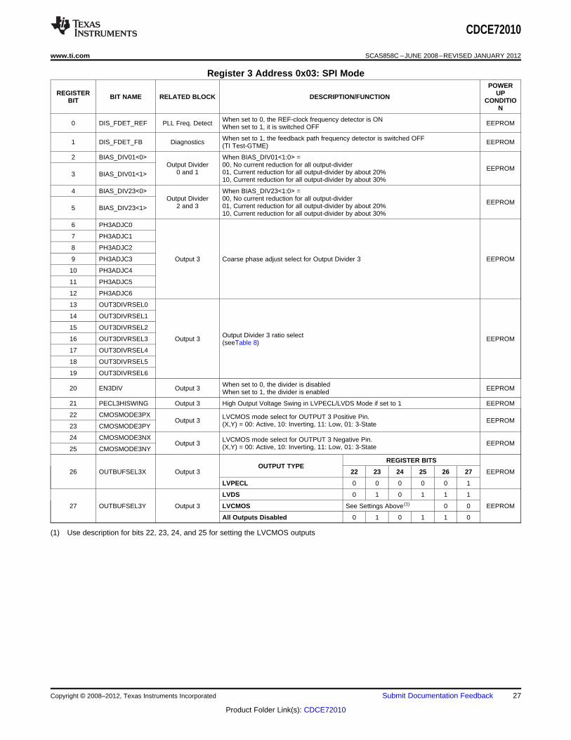
Register 3 Address 0x03: SPI ModePOWER
REGISTER UPBIT NAME RELATED BLOCK DESCRIPTION/FUNCTIONBIT CONDITION
When set to 0, the REF-clock frequency detector is ON0 DIS_FDET_REF PLL Freq. Detect EEPROMWhen set to 1, it is switched OFF
When set to 1, the feedback path frequency detector is switched OFF1 DIS_FDET_FB Diagnostics EEPROM(TI Test-GTME)
2 BIAS_DIV01<0> When BIAS_DIV01<1:0> =Output Divider 00, No current reduction for all output-divider EEPROM0 and 1 01, Current reduction for all output-divider by about 20%3 BIAS_DIV01<1>
10, Current reduction for all output-divider by about 30%
4 BIAS_DIV23<0> When BIAS_DIV23<1:0> =Output Divider 00, No current reduction for all output-divider EEPROM2 and 3 01, Current reduction for all output-divider by about 20%5 BIAS_DIV23<1>
10, Current reduction for all output-divider by about 30%
6 PH3ADJC0
7 PH3ADJC1
8 PH3ADJC2
9 PH3ADJC3 Output 3 Coarse phase adjust select for Output Divider 3 EEPROM
10 PH3ADJC4
11 PH3ADJC5
12 PH3ADJC6
13 OUT3DIVRSEL0
14 OUT3DIVRSEL1
15 OUT3DIVRSEL2Output Divider 3 ratio select16 OUT3DIVRSEL3 Output 3 EEPROM(seeTable 8)
17 OUT3DIVRSEL4
18 OUT3DIVRSEL5
19 OUT3DIVRSEL6
When set to 0, the divider is disabled20 EN3DIV Output 3 EEPROMWhen set to 1, the divider is enabled
21 PECL3HISWING Output 3 High Output Voltage Swing in LVPECL/LVDS Mode if set to 1 EEPROM
22 CMOSMODE3PX LVCMOS mode select for OUTPUT 3 Positive Pin.Output 3 EEPROM(X,Y) = 00: Active, 10: Inverting, 11: Low, 01: 3-State23 CMOSMODE3PY
24 CMOSMODE3NX LVCMOS mode select for OUTPUT 3 Negative Pin.Output 3 EEPROM(X,Y) = 00: Active, 10: Inverting, 11: Low, 01: 3-State25 CMOSMODE3NY
REGISTER BITSOUTPUT TYPE
26 OUTBUFSEL3X Output 3 22 23 24 25 26 27 EEPROM
LVPECL 0 0 0 0 0 1
LVDS 0 1 0 1 1 1
27 OUTBUFSEL3Y Output 3 LVCMOS See Settings Above (1) 0 0 EEPROM
All Outputs Disabled 0 1 0 1 1 0
(1) Use description for bits 22, 23, 24, and 25 for setting the LVCMOS outputs
Copyright © 2008–2012, Texas Instruments Incorporated Submit Documentation Feedback 27
Product Folder Link(s): CDCE72010
CDCE72010
SCAS858C –JUNE 2008–REVISED JANUARY 2012 www.ti.com
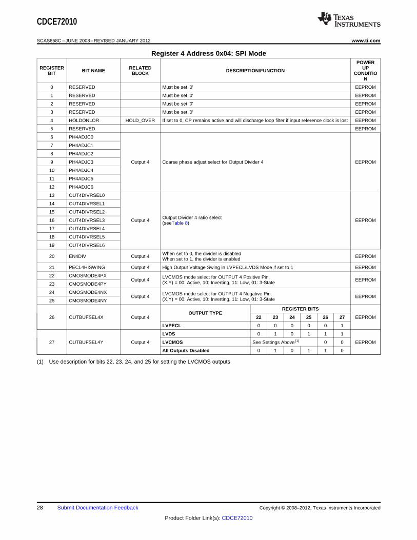
Register 4 Address 0x04: SPI ModePOWER
REGISTER RELATED UPBIT NAME DESCRIPTION/FUNCTIONBIT BLOCK CONDITION
0 RESERVED Must be set '0' EEPROM
1 RESERVED Must be set '0' EEPROM
2 RESERVED Must be set '0' EEPROM
3 RESERVED Must be set '0' EEPROM
4 HOLDONLOR HOLD_OVER If set to 0, CP remains active and will discharge loop filter if input reference clock is lost EEPROM
5 RESERVED EEPROM
6 PH4ADJC0
7 PH4ADJC1
8 PH4ADJC2
9 PH4ADJC3 Output 4 Coarse phase adjust select for Output Divider 4 EEPROM
10 PH4ADJC4
11 PH4ADJC5
12 PH4ADJC6
13 OUT4DIVRSEL0
14 OUT4DIVRSEL1
15 OUT4DIVRSEL2Output Divider 4 ratio select16 OUT4DIVRSEL3 Output 4 EEPROM(seeTable 8)
17 OUT4DIVRSEL4
18 OUT4DIVRSEL5
19 OUT4DIVRSEL6
When set to 0, the divider is disabled20 EN4DIV Output 4 EEPROMWhen set to 1, the divider is enabled
21 PECL4HISWING Output 4 High Output Voltage Swing in LVPECL/LVDS Mode if set to 1 EEPROM
22 CMOSMODE4PX LVCMOS mode select for OUTPUT 4 Positive Pin.Output 4 EEPROM(X,Y) = 00: Active, 10: Inverting, 11: Low, 01: 3-State23 CMOSMODE4PY
24 CMOSMODE4NX LVCMOS mode select for OUTPUT 4 Negative Pin.Output 4 EEPROM(X,Y) = 00: Active, 10: Inverting, 11: Low, 01: 3-State25 CMOSMODE4NY
REGISTER BITSOUTPUT TYPE
26 OUTBUFSEL4X Output 4 22 23 24 25 26 27 EEPROM
LVPECL 0 0 0 0 0 1
LVDS 0 1 0 1 1 1
27 OUTBUFSEL4Y Output 4 LVCMOS See Settings Above (1) 0 0 EEPROM
All Outputs Disabled 0 1 0 1 1 0
(1) Use description for bits 22, 23, 24, and 25 for setting the LVCMOS outputs
28 Submit Documentation Feedback Copyright © 2008–2012, Texas Instruments Incorporated
Product Folder Link(s): CDCE72010
CDCE72010
www.ti.com SCAS858C –JUNE 2008–REVISED JANUARY 2012
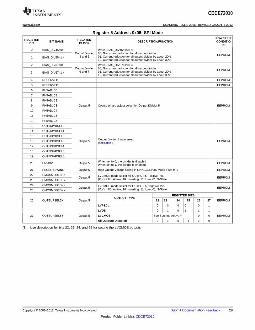
Register 5 Address 0x05: SPI ModePOWER UPREGISTER RELATEDBIT NAME DESCRIPTION/FUNCTION CONDITIOBIT BLOCK N
0 BIAS_DIV45<0> When BIAS_DIV45<1:0> =Output Divider 00, No current reduction for all output-divider EEPROM4 and 5 01, Current reduction for all output-divider by about 20%1 BIAS_DIV45<1>
10, Current reduction for all output-divider by about 30%
2 BIAS_DIV67<0> When BIAS_DIV67<1:0> =Output Divider 00, No current reduction for all output-divider EEPROM6 and 7 01, Current reduction for all output-divider by about 20%3 BIAS_DIV67<1>
10, Current reduction for all output-divider by about 30%
4 RESERVED EEPROM
5 RESERVED EEPROM
6 PH5ADJC0
7 PH5ADJC1
8 PH5ADJC2
9 PH5ADJC3 Output 5 Coarse phase adjust select for Output Divider 5 EEPROM
10 PH5ADJC4
11 PH5ADJC5
12 PH5ADJC6
13 OUT5DIVRSEL0
14 OUT5DIVRSEL1
15 OUT5DIVRSEL2Output Divider 5 ratio select16 OUT5DIVRSEL3 Output 5 EEPROM(seeTable 8)
17 OUT5DIVRSEL4
18 OUT5DIVRSEL5
19 OUT5DIVRSEL6
When set to 0, the divider is disabled20 EN5DIV Output 5 EEPROMWhen set to 1, the divider is enabled
21 PECL5HISWING Output 5 High Output Voltage Swing in LVPECL/LVDS Mode if set to 1 EEPROM
22 CMOSMODE5PX LVCMOS mode select for OUTPUT 5 Positive Pin.Output 5 EEPROM(X,Y) = 00: Active, 10: Inverting, 11: Low, 01: 3-State23 CMOSMODE5PY
24 CMOSMODE5NX LVCMOS mode select for OUTPUT 5 Negative Pin.Output 5 EEPROM(X,Y) = 00: Active, 10: Inverting, 11: Low, 01: 3-State25 CMOSMODE5NY
REGISTER BITSOUTPUT TYPE
26 OUTBUFSEL5X Output 5 22 23 24 25 26 27 EEPROM
LVPECL 0 0 0 0 0 1
LVDS 0 1 0 1 1 1
27 OUTBUFSEL5Y Output 5 LVCMOS See Settings Above (1) 0 0 EEPROM
All Outputs Disabled 0 1 0 1 1 0
(1) Use description for bits 22, 23, 24, and 25 for setting the LVCMOS outputs
Copyright © 2008–2012, Texas Instruments Incorporated Submit Documentation Feedback 29
Product Folder Link(s): CDCE72010
CDCE72010
SCAS858C –JUNE 2008–REVISED JANUARY 2012 www.ti.com
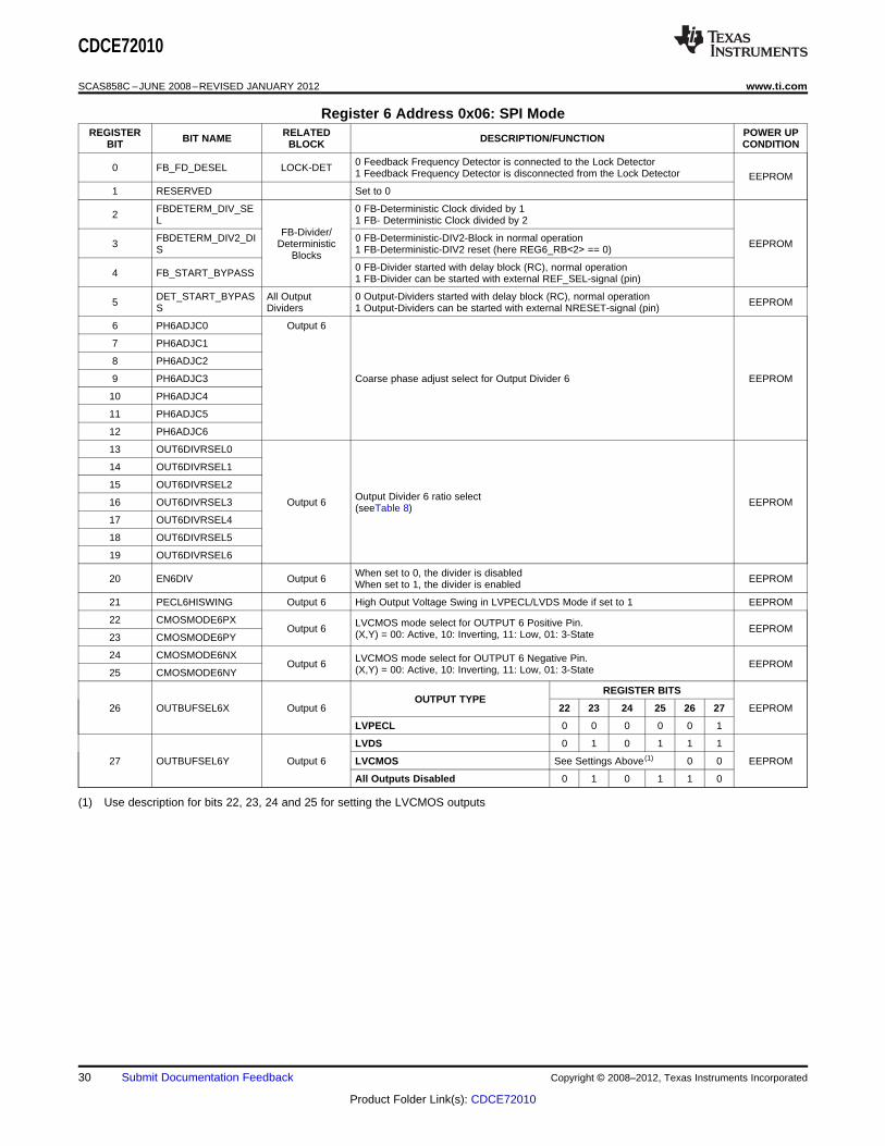
Register 6 Address 0x06: SPI ModeREGISTER RELATED POWER UPBIT NAME DESCRIPTION/FUNCTIONBIT BLOCK CONDITION
0 Feedback Frequency Detector is connected to the Lock Detector0 FB_FD_DESEL LOCK-DET 1 Feedback Frequency Detector is disconnected from the Lock Detector EEPROM1 RESERVED Set to 0
FBDETERM_DIV_SE 0 FB-Deterministic Clock divided by 12 L 1 FB- Deterministic Clock divided by 2FB-Divider/FBDETERM_DIV2_DI 0 FB-Deterministic-DIV2-Block in normal operation3 Deterministic EEPROMS 1 FB-Deterministic-DIV2 reset (here REG6_RB<2> == 0)Blocks
0 FB-Divider started with delay block (RC), normal operation4 FB_START_BYPASS 1 FB-Divider can be started with external REF_SEL-signal (pin)
DET_START_BYPAS All Output 0 Output-Dividers started with delay block (RC), normal operation5 EEPROMS Dividers 1 Output-Dividers can be started with external NRESET-signal (pin)
6 PH6ADJC0 Output 6
7 PH6ADJC1
8 PH6ADJC2
9 PH6ADJC3 Coarse phase adjust select for Output Divider 6 EEPROM
10 PH6ADJC4
11 PH6ADJC5
12 PH6ADJC6
13 OUT6DIVRSEL0
14 OUT6DIVRSEL1
15 OUT6DIVRSEL2Output Divider 6 ratio select16 OUT6DIVRSEL3 Output 6 EEPROM(seeTable 8)
17 OUT6DIVRSEL4
18 OUT6DIVRSEL5
19 OUT6DIVRSEL6
When set to 0, the divider is disabled20 EN6DIV Output 6 EEPROMWhen set to 1, the divider is enabled
21 PECL6HISWING Output 6 High Output Voltage Swing in LVPECL/LVDS Mode if set to 1 EEPROM
22 CMOSMODE6PX LVCMOS mode select for OUTPUT 6 Positive Pin.Output 6 EEPROM(X,Y) = 00: Active, 10: Inverting, 11: Low, 01: 3-State23 CMOSMODE6PY
24 CMOSMODE6NX LVCMOS mode select for OUTPUT 6 Negative Pin.Output 6 EEPROM(X,Y) = 00: Active, 10: Inverting, 11: Low, 01: 3-State25 CMOSMODE6NY
REGISTER BITSOUTPUT TYPE
26 OUTBUFSEL6X Output 6 22 23 24 25 26 27 EEPROM
LVPECL 0 0 0 0 0 1
LVDS 0 1 0 1 1 1
27 OUTBUFSEL6Y Output 6 LVCMOS See Settings Above (1) 0 0 EEPROM
All Outputs Disabled 0 1 0 1 1 0
(1) Use description for bits 22, 23, 24 and 25 for setting the LVCMOS outputs
30 Submit Documentation Feedback Copyright © 2008–2012, Texas Instruments Incorporated
Product Folder Link(s): CDCE72010
CDCE72010
www.ti.com SCAS858C –JUNE 2008–REVISED JANUARY 2012
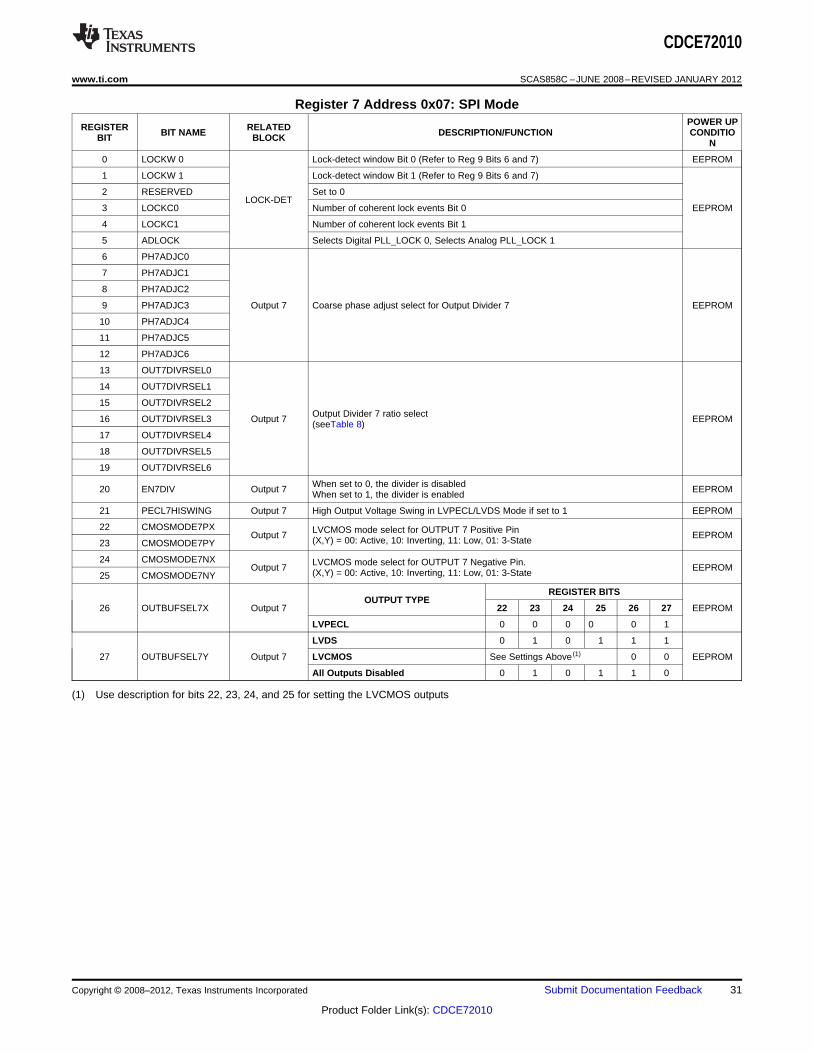
Register 7 Address 0x07: SPI ModePOWER UPREGISTER RELATEDBIT NAME DESCRIPTION/FUNCTION CONDITIOBIT BLOCK N
0 LOCKW 0 Lock-detect window Bit 0 (Refer to Reg 9 Bits 6 and 7) EEPROM
1 LOCKW 1 Lock-detect window Bit 1 (Refer to Reg 9 Bits 6 and 7)
2 RESERVED Set to 0LOCK-DET
3 LOCKC0 Number of coherent lock events Bit 0 EEPROM
4 LOCKC1 Number of coherent lock events Bit 1
5 ADLOCK Selects Digital PLL_LOCK 0, Selects Analog PLL_LOCK 1
6 PH7ADJC0
7 PH7ADJC1
8 PH7ADJC2
9 PH7ADJC3 Output 7 Coarse phase adjust select for Output Divider 7 EEPROM
10 PH7ADJC4
11 PH7ADJC5
12 PH7ADJC6
13 OUT7DIVRSEL0
14 OUT7DIVRSEL1
15 OUT7DIVRSEL2Output Divider 7 ratio select16 OUT7DIVRSEL3 Output 7 EEPROM(seeTable 8)
17 OUT7DIVRSEL4
18 OUT7DIVRSEL5
19 OUT7DIVRSEL6
When set to 0, the divider is disabled20 EN7DIV Output 7 EEPROMWhen set to 1, the divider is enabled
21 PECL7HISWING Output 7 High Output Voltage Swing in LVPECL/LVDS Mode if set to 1 EEPROM
22 CMOSMODE7PX LVCMOS mode select for OUTPUT 7 Positive PinOutput 7 EEPROM(X,Y) = 00: Active, 10: Inverting, 11: Low, 01: 3-State23 CMOSMODE7PY
24 CMOSMODE7NX LVCMOS mode select for OUTPUT 7 Negative Pin.Output 7 EEPROM(X,Y) = 00: Active, 10: Inverting, 11: Low, 01: 3-State25 CMOSMODE7NY
REGISTER BITSOUTPUT TYPE
26 OUTBUFSEL7X Output 7 22 23 24 25 26 27 EEPROM
LVPECL 0 0 0 0 0 1
LVDS 0 1 0 1 1 1
27 OUTBUFSEL7Y Output 7 LVCMOS See Settings Above (1) 0 0 EEPROM
All Outputs Disabled 0 1 0 1 1 0
(1) Use description for bits 22, 23, 24, and 25 for setting the LVCMOS outputs
Copyright © 2008–2012, Texas Instruments Incorporated Submit Documentation Feedback 31
Product Folder Link(s): CDCE72010
CDCE72010
SCAS858C –JUNE 2008–REVISED JANUARY 2012 www.ti.com
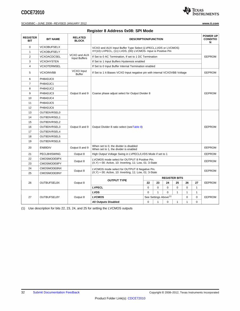
Register 8 Address 0x08: SPI ModePOWER UPREGISTER RELATEDBIT NAME DESCRIPTION/FUNCTION CONDITIOBIT BLOCK N
0 VCXOBUFSELX VCXO and AUX Input Buffer Type Select (LVPECL,LVDS or LVCMOS)XY(10) LVPECL, (11) LVDS, (00) LVCMOS- Input is Positive Pin1 VCXOBUFSELY
VCXO and AUX2 VCXOACDCSEL If Set to 0 AC Termination, If set to 1 DC Termination EEPROMInput Buffers3 VCXOHYSTEN If Set to 1 Input Buffers Hysteresis enabled
4 VCXOTERMSEL If Set to 0 Input Buffer Internal Termination enabled
VCXO Input5 VCXOINVBB If Set to 1 It Biases VCXO Input negative pin with internal VCXOVBB Voltage EEPROMBuffer
6 PH8ADJC0
7 PH8ADJC1
8 PH8ADJC2
9 PH8ADJC3 Output 8 and 9 Coarse phase adjust select for Output Divider 8 EEPROM
10 PH8ADJC4
11 PH8ADJC5
12 PH8ADJC6
13 OUT8DIVRSEL0
14 OUT8DIVRSEL1
15 OUT8DIVRSEL2
16 OUT8DIVRSEL3 Output 8 and 9 Output Divider 8 ratio select (seeTable 8) EEPROM
17 OUT8DIVRSEL4
18 OUT8DIVRSEL5
19 OUT8DIVRSEL6
When set to 0, the divider is disabled20 EN89DIV Output 8 and 9 EEPROMWhen set to 1, the divider is enabled
21 PECL8HISWING Output 8 High Output Voltage Swing in LVPECL/LVDS Mode if set to 1 EEPROM
22 CMOSMODE8PX LVCMOS mode select for OUTPUT 8 Positive Pin.Output 8 EEPROM(X,Y) = 00: Active, 10: Inverting, 11: Low, 01: 3-State23 CMOSMODE8PY
24 CMOSMODE8NX LVCMOS mode select for OUTPUT 8 Negative Pin.Output 8 EEPROM(X,Y) = 00: Active, 10: Inverting, 11: Low, 01: 3-State25 CMOSMODE8NY
REGISTER BITSOUTPUT TYPE
26 OUTBUFSEL8X Output 8 22 23 24 25 26 27 EEPROM
LVPECL 0 0 0 0 0 1
LVDS 0 1 0 1 1 1
27 OUTBUFSEL8Y Output 8 LVCMOS See Settings Above (1) 0 0 EEPROM
All Outputs Disabled 0 1 0 1 1 0
(1) Use description for bits 22, 23, 24, and 25 for setting the LVCMOS outputs
32 Submit Documentation Feedback Copyright © 2008–2012, Texas Instruments Incorporated
Product Folder Link(s): CDCE72010
CDCE72010
www.ti.com SCAS858C –JUNE 2008–REVISED JANUARY 2012
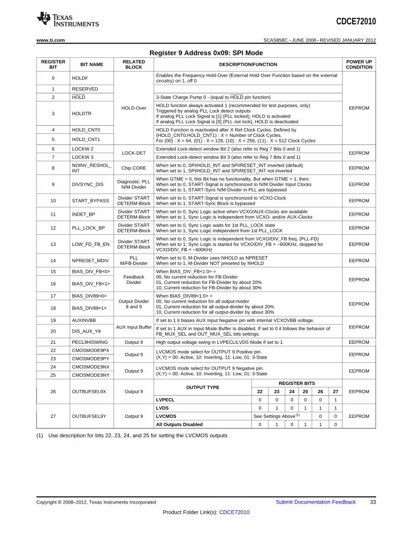
Register 9 Address 0x09: SPI ModeREGISTER RELATED POWER UPBIT NAME DESCRIPTION/FUNCTIONBIT BLOCK CONDITION
Enables the Frequency Hold-Over (External Hold Over Function based on the external0 HOLDF circuitry) on 1, off 0
1 RESERVED
2 HOLD 3-State Charge Pump 0 - (equal to HOLD pin function)
HOLD function always activated 1 (recommended for test purposes, only)HOLD-Over EEPROMTriggered by analog PLL Lock detect outputs3 HOLDTR If analog PLL Lock Signal is [1] (PLL locked), HOLD is activatedIf analog PLL Lock Signal is [0] (PLL not lock), HOLD is deactivated
4 HOLD_CNT0 HOLD Function is reactivated after X Ref Clock Cycles. Defined by(HOLD_CNT0,HOLD_CNT1) : X = Number of Clock Cycles.
5 HOLD_CNT1 For (00) : X = 64, (01) : X = 128, (10) : X = 256, (11) : X = 512 Clock Cycles
6 LOCKW 2 Extended Lock-detect window Bit 2 (also refer to Reg 7 Bits 0 and 1)LOCK-DET EEPROM
7 LOCKW 3 Extended Lock-detect window Bit 3 (also refer to Reg 7 Bits 0 and 1)
NOINV_RESHOL_ When set to 0, SPI/HOLD_INT and SPI/RESET_INT inverted (default)8 Chip CORE EEPROMINT When set to 1, SPI/HOLD_INT and SPI/RESET_INT not inverted
When GTME = 0, this Bit has no functionality, But when GTME = 1, then:Diagnostic: PLL9 DIVSYNC_DIS When set to 0, START-Signal is synchronized to N/M Divider Input Clocks EEPROMN/M Divider When set to 1, START-Sync N/M Divider in PLL are bypassed
Divider START When set to 0, START-Signal is synchronized to VCXO-Clock10 START_BYPASS EEPROMDETERM-Block When set to 1, START-Sync Block is bypassed
Divider START When set to 0, Sync Logic active when VCXO/AUX-Clocks are available11 INDET_BP EEPROMDETERM-Block When set to 1, Sync Logic is independent from VCXO- and/or AUX-Clocks
Divider START When set to 0, Sync Logic waits for 1st PLL_LOCK state12 PLL_LOCK_BP EEPROMDETERM-Block When set to 1, Sync Logic independent from 1st PLL_LOCK
When set to 0, Sync Logic is independent from VCXO/DIV_FB freq. (PLL-FD)Divider START13 LOW_FD_FB_EN When set to 1, Sync Logic is started for VCXO/DIV_FB > ~600KHz, stopped for EEPROMDETERM-Block VCXO/DIV_FB < ~600KHz
PLL When set to 0, M-Divider uses NHOLD as NPRESET14 NPRESET_MDIV EEPROMM/FB-Divider When set to 1, M-Divider NOT preseted by NHOLD
15 BIAS_DIV_FB<0> When BIAS_DIV_FB<1:0> =Feedback 00, No current reduction for FB-Divider EEPROMDivider 01, Current reduction for FB-Divider by about 20%16 BIAS_DIV_FB<1>
10, Current reduction for FB-Divider by about 30%
17 BIAS_DIV89<0> When BIAS_DIV89<1:0> =Output Divider 00, No current reduction for all output-rivider EEPROM8 and 9 01, Current reduction for all output-divider by about 20%18 BIAS_DIV89<1>
10, Current reduction for all output-divider by about 30%
19 AUXINVBB If set to 1 it biases AUX Input Negative pin with internal VCXOVBB voltage.AUX Input Buffer EEPROMIf set to 1 AUX in Input Mode Buffer Is disabled. If set to 0 it follows the behavior of20 DIS_AUX_Y9 FB_MUX_SEL and OUT_MUX_SEL bits settings.
21 PECL9HISWING Output 9 High output voltage swing in LVPECL/LVDS Mode if set to 1 EEPROM
22 CMOSMODE9PX LVCMOS mode select for OUTPUT 9 Positive pin.Output 9 EEPROM(X,Y) = 00: Active, 10: Inverting, 11: Low, 01: 3-State23 CMOSMODE9PY
24 CMOSMODE9NX LVCMOS mode select for OUTPUT 9 Negative pin.Output 9 EEPROM(X,Y) = 00: Active, 10: Inverting, 11: Low, 01: 3-State25 CMOSMODE9NY
REGISTER BITSOUTPUT TYPE
26 OUTBUFSEL9X Output 9 22 23 24 25 26 27 EEPROM
LVPECL 0 0 0 0 0 1
LVDS 0 1 0 1 1 1
27 OUTBUFSEL9Y Output 9 LVCMOS See Settings Above (1) 0 0 EEPROM
All Outputs Disabled 0 1 0 1 1 0
(1) Use description for bits 22, 23, 24, and 25 for setting the LVCMOS outputs
Copyright © 2008–2012, Texas Instruments Incorporated Submit Documentation Feedback 33
Product Folder Link(s): CDCE72010
CDCE72010
SCAS858C –JUNE 2008–REVISED JANUARY 2012 www.ti.com
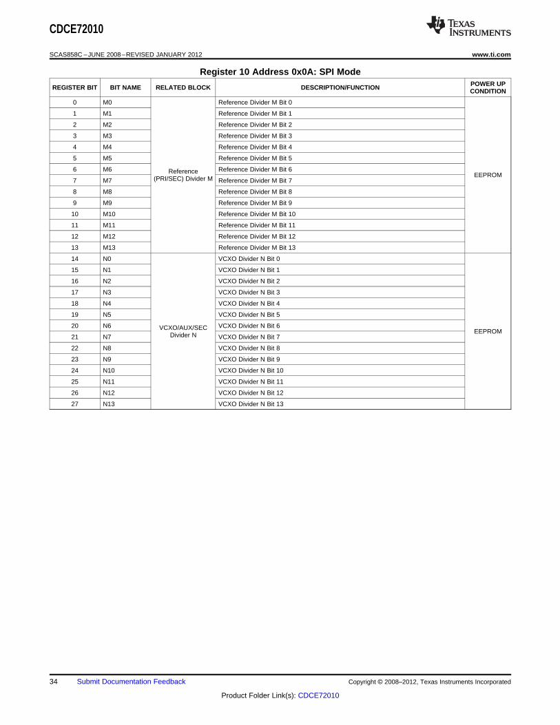
Register 10 Address 0x0A: SPI ModePOWER UPREGISTER BIT BIT NAME RELATED BLOCK DESCRIPTION/FUNCTION CONDITION
0 M0 Reference Divider M Bit 0
1 M1 Reference Divider M Bit 1
2 M2 Reference Divider M Bit 2
3 M3 Reference Divider M Bit 3
4 M4 Reference Divider M Bit 4
5 M5 Reference Divider M Bit 5
6 M6 Reference Divider M Bit 6Reference EEPROM(PRI/SEC) Divider M7 M7 Reference Divider M Bit 7
8 M8 Reference Divider M Bit 8
9 M9 Reference Divider M Bit 9
10 M10 Reference Divider M Bit 10
11 M11 Reference Divider M Bit 11
12 M12 Reference Divider M Bit 12
13 M13 Reference Divider M Bit 13
14 N0 VCXO Divider N Bit 0
15 N1 VCXO Divider N Bit 1
16 N2 VCXO Divider N Bit 2
17 N3 VCXO Divider N Bit 3
18 N4 VCXO Divider N Bit 4
19 N5 VCXO Divider N Bit 5
20 N6 VCXO Divider N Bit 6VCXO/AUX/SEC EEPROMDivider N21 N7 VCXO Divider N Bit 7
22 N8 VCXO Divider N Bit 8
23 N9 VCXO Divider N Bit 9
24 N10 VCXO Divider N Bit 10
25 N11 VCXO Divider N Bit 11
26 N12 VCXO Divider N Bit 12
27 N13 VCXO Divider N Bit 13
34 Submit Documentation Feedback Copyright © 2008–2012, Texas Instruments Incorporated
Product Folder Link(s): CDCE72010
CDCE72010
www.ti.com SCAS858C –JUNE 2008–REVISED JANUARY 2012
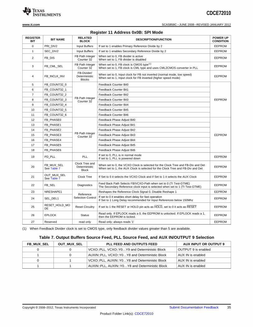
Register 11 Address 0x0B: SPI ModeREGISTER RELATED POWER UPBIT NAME DESCRIPTION/FUNCTIONBIT BLOCK CONDITION
0 PRI_DIV2 Input Buffers If set to 1 enables Primary Reference Divide by 2 EEPROM
1 SEC_DIV2 Input Buffers If set to 1 enables Secondary Reference Divide by 2 EEPROM
FB Path Integer When set to 0, FB divider is active2 FB_DIS EEPROMCounter 32 When set to 1, FB divider is disabled
FB Path Integer When set to 0, FB clock is CMOS type (1)3 FB_CML_SEL EEPROMCounter 32 When set to 1, FB clock is CML type and uses CML2CMOS converter in PLL
FB-Divider/ When set to 0, Input clock for FB not inverted (normal mode, low speed)4 FB_INCLK_INV Deterministic EEPROMWhen set to 1, Input clock for FB inverted (higher speed mode)Blocks
5 FB_COUNT32_0 Feedback Counter Bit0
6 FB_COUNT32_1 Feedback Counter Bit1
7 FB_COUNT32_2 Feedback Counter Bit2FB Path Integer8 FB_COUNT32_3 Feedback Counter Bit3 EEPROMCounter 32
9 FB_COUNT32_4 Feedback Counter Bit4
10 FB_COUNT32_5 Feedback Counter Bit5
11 FB_COUNT32_6 Feedback Counter Bit6
12 FB_PHASE0 Feedback Phase Adjust Bit0
13 FB_PHASE1 Feedback Phase Adjust Bit1
14 FB_PHASE2 Feedback Phase Adjust Bit2FB Path Integer15 FB_PHASE3 Feedback Phase Adjust Bit3 EEPROMCounter 32
16 FB_PHASE4 Feedback Phase Adjust Bit4
17 FB_PHASE5 Feedback Phase Adjust Bit5
18 FB_PHASE6 Feedback Phase Adjust Bit6
If set to 0, PLL is in normal mode19 PD_PLL PLL EEPROMIf set to 1, PLL is powered down
Clock Tree andFB_MUX_SEL When set to 0, the VCXO Clock is selected for the Clock Tree and FB-Div and Det20 Deterministic EEPROMSee Table 7 When set to 1, the AUX Clock is selected for the Clock Tree and FB-Div and DetBlock
OUT_MUX_SEL21 Clock Tree If Set to 0 it selects the VCXO Clock and if Set to 1 it selects the AUX Clock EEPROMSee Table 7
Feed Back Path Selects FB/VCXO-Path when set to 0 (TI Test-GTME)22 FB_SEL Diagnostics EEPROMThe Secondary Reference clock input is selected when set to 1 (TI Test-GTME)
23 NRESHAPE1 Reshapes the Reference Clock Signal 0, Disable Reshape 1 EEPROMReference
If set to 0 it enables short delay for fast operationSelection Control24 SEL_DEL1 EEPROMIf Set to 1 Long Delay recommended for Input References below 150Mhz
RESET_HOLD_MO25 Reset Circuitry If set to 1 the RESET or HOLD pin acts as HOLD, set to 0 it acts as RESET EEPROMDE
Read only. If EPLOCK reads a 0, the EEPROM is unlocked. If EPLOCK reads a 1,26 EPLOCK Status EEPROMthen the EEPROM is locked.
27 Reserved read only Read only; always reads '1' EEPROM
(1) When Feedback Divider clock is set to CMOS type, only feedback divider values greater than 5 are available.
Table 7. Output Buffers Source Feed, PLL Source Feed, and AUX IN/OUTPUT 9 Selection
FB_MUX_SEL OUT_MUX_SEL PLL FEED AND OUTPUTS FEED AUX INPUT OR OUTPUT 9
0 0 VCXO::PLL, VCXO::Y0…Y9 and Deterministic Block OUTPUT 9 is enabled
1 0 AUXIN::PLL, VCXO::Y0…Y8 and Deterministic Block AUX IN is enabled
0 1 VCXO::PLL, AUXIN::Y0…Y8 and Deterministic Block AUX IN is enabled
1 1 AUXIN::PLL, AUXIN::Y0…Y8 and Deterministic Block AUX IN is enabled
Copyright © 2008–2012, Texas Instruments Incorporated Submit Documentation Feedback 35
Product Folder Link(s): CDCE72010
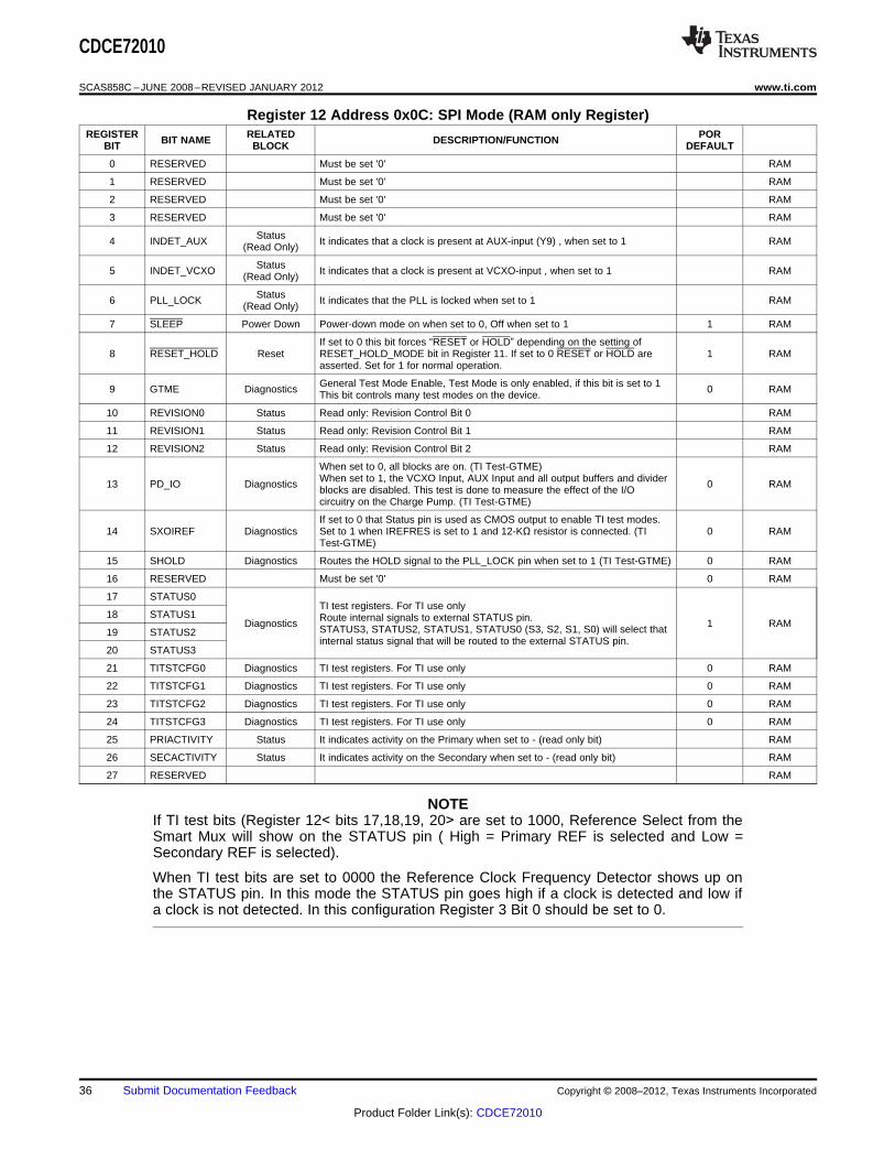
CDCE72010
SCAS858C –JUNE 2008–REVISED JANUARY 2012 www.ti.com
Register 12 Address 0x0C: SPI Mode (RAM only Register)REGISTER RELATED PORBIT NAME DESCRIPTION/FUNCTIONBIT BLOCK DEFAULT
0 RESERVED Must be set '0' RAM
1 RESERVED Must be set '0' RAM
2 RESERVED Must be set '0' RAM
3 RESERVED Must be set '0' RAM
Status4 INDET_AUX It indicates that a clock is present at AUX-input (Y9) , when set to 1 RAM(Read Only)
Status5 INDET_VCXO It indicates that a clock is present at VCXO-input , when set to 1 RAM(Read Only)
Status6 PLL_LOCK It indicates that the PLL is locked when set to 1 RAM(Read Only)
7 SLEEP Power Down Power-down mode on when set to 0, Off when set to 1 1 RAM
If set to 0 this bit forces “RESET or HOLD” depending on the setting of8 RESET_HOLD Reset RESET_HOLD_MODE bit in Register 11. If set to 0 RESET or HOLD are 1 RAM
asserted. Set for 1 for normal operation.
General Test Mode Enable, Test Mode is only enabled, if this bit is set to 19 GTME Diagnostics 0 RAMThis bit controls many test modes on the device.
10 REVISION0 Status Read only: Revision Control Bit 0 RAM
11 REVISION1 Status Read only: Revision Control Bit 1 RAM
12 REVISION2 Status Read only: Revision Control Bit 2 RAM
When set to 0, all blocks are on. (TI Test-GTME)When set to 1, the VCXO Input, AUX Input and all output buffers and divider13 PD_IO Diagnostics 0 RAMblocks are disabled. This test is done to measure the effect of the I/Ocircuitry on the Charge Pump. (TI Test-GTME)
If set to 0 that Status pin is used as CMOS output to enable TI test modes.14 SXOIREF Diagnostics Set to 1 when IREFRES is set to 1 and 12-KΩ resistor is connected. (TI 0 RAM
Test-GTME)
15 SHOLD Diagnostics Routes the HOLD signal to the PLL_LOCK pin when set to 1 (TI Test-GTME) 0 RAM
16 RESERVED Must be set '0' 0 RAM
17 STATUS0TI test registers. For TI use only
18 STATUS1 Route internal signals to external STATUS pin.Diagnostics 1 RAMSTATUS3, STATUS2, STATUS1, STATUS0 (S3, S2, S1, S0) will select that19 STATUS2internal status signal that will be routed to the external STATUS pin.
20 STATUS3
21 TITSTCFG0 Diagnostics TI test registers. For TI use only 0 RAM
22 TITSTCFG1 Diagnostics TI test registers. For TI use only 0 RAM
23 TITSTCFG2 Diagnostics TI test registers. For TI use only 0 RAM
24 TITSTCFG3 Diagnostics TI test registers. For TI use only 0 RAM
25 PRIACTIVITY Status It indicates activity on the Primary when set to - (read only bit) RAM
26 SECACTIVITY Status It indicates activity on the Secondary when set to - (read only bit) RAM
27 RESERVED RAM
NOTEIf TI test bits (Register 12< bits 17,18,19, 20> are set to 1000, Reference Select from theSmart Mux will show on the STATUS pin ( High = Primary REF is selected and Low =Secondary REF is selected).
When TI test bits are set to 0000 the Reference Clock Frequency Detector shows up onthe STATUS pin. In this mode the STATUS pin goes high if a clock is detected and low ifa clock is not detected. In this configuration Register 3 Bit 0 should be set to 0.
36 Submit Documentation Feedback Copyright © 2008–2012, Texas Instruments Incorporated
Product Folder Link(s): CDCE72010
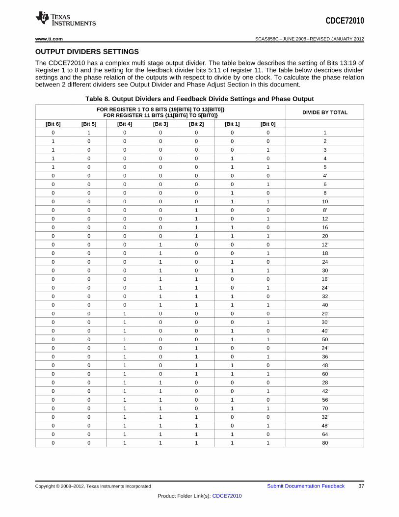
CDCE72010
www.ti.com SCAS858C –JUNE 2008–REVISED JANUARY 2012
OUTPUT DIVIDERS SETTINGS
The CDCE72010 has a complex multi stage output divider. The table below describes the setting of Bits 13:19 ofRegister 1 to 8 and the setting for the feedback divider bits 5:11 of register 11. The table below describes dividersettings and the phase relation of the outputs with respect to divide by one clock. To calculate the phase relationbetween 2 different dividers see Output Divider and Phase Adjust Section in this document.
Table 8. Output Dividers and Feedback Divide Settings and Phase Output
FOR REGISTER 1 TO 8 BITS 19[BIT6] TO 13[BIT0] DIVIDE BY TOTALFOR REGISTER 11 BITS 11[BIT6] TO 5[BIT0]
[Bit 6] [Bit 5] [Bit 4] [Bit 3] [Bit 2] [Bit 1] [Bit 0]
0 1 0 0 0 0 0 1
1 0 0 0 0 0 0 2
1 0 0 0 0 0 1 3
1 0 0 0 0 1 0 4
1 0 0 0 0 1 1 5
0 0 0 0 0 0 0 4'
0 0 0 0 0 0 1 6
0 0 0 0 0 1 0 8
0 0 0 0 0 1 1 10
0 0 0 0 1 0 0 8'
0 0 0 0 1 0 1 12
0 0 0 0 1 1 0 16
0 0 0 0 1 1 1 20
0 0 0 1 0 0 0 12'
0 0 0 1 0 0 1 18
0 0 0 1 0 1 0 24
0 0 0 1 0 1 1 30
0 0 0 1 1 0 0 16'
0 0 0 1 1 0 1 24'
0 0 0 1 1 1 0 32
0 0 0 1 1 1 1 40
0 0 1 0 0 0 0 20'
0 0 1 0 0 0 1 30'
0 0 1 0 0 1 0 40'
0 0 1 0 0 1 1 50
0 0 1 0 1 0 0 24'
0 0 1 0 1 0 1 36
0 0 1 0 1 1 0 48
0 0 1 0 1 1 1 60
0 0 1 1 0 0 0 28
0 0 1 1 0 0 1 42
0 0 1 1 0 1 0 56
0 0 1 1 0 1 1 70
0 0 1 1 1 0 0 32'
0 0 1 1 1 0 1 48'
0 0 1 1 1 1 0 64
0 0 1 1 1 1 1 80
Copyright © 2008–2012, Texas Instruments Incorporated Submit Documentation Feedback 37
Product Folder Link(s): CDCE72010
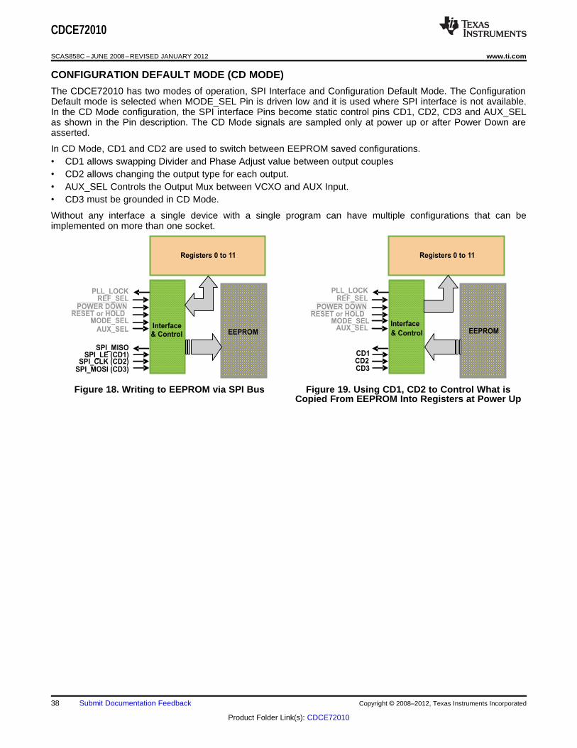
EEPROM
PLL_LOCKREF_SEL
POWER DOWNRESET HOLDor
MODE_SELAUX_SEL
SPI_MISOSPI_LE (CD1)
SPI_CLK (CD2)SPI_MOSI (CD3)
Interface& Control
Registers 0 to 11
PLL_LOCKREF_SEL
POWER DOWNRESET HOLDor
MODE_SELAUX_SEL
CD1CD2CD3
EEPROMInterface
& Control
Registers 0 to 11
CDCE72010
SCAS858C –JUNE 2008–REVISED JANUARY 2012 www.ti.com
CONFIGURATION DEFAULT MODE (CD MODE)
The CDCE72010 has two modes of operation, SPI Interface and Configuration Default Mode. The ConfigurationDefault mode is selected when MODE_SEL Pin is driven low and it is used where SPI interface is not available.In the CD Mode configuration, the SPI interface Pins become static control pins CD1, CD2, CD3 and AUX_SELas shown in the Pin description. The CD Mode signals are sampled only at power up or after Power Down areasserted.
In CD Mode, CD1 and CD2 are used to switch between EEPROM saved configurations.• CD1 allows swapping Divider and Phase Adjust value between output couples• CD2 allows changing the output type for each output.• AUX_SEL Controls the Output Mux between VCXO and AUX Input.• CD3 must be grounded in CD Mode.
Without any interface a single device with a single program can have multiple configurations that can beimplemented on more than one socket.
Figure 18. Writing to EEPROM via SPI Bus Figure 19. Using CD1, CD2 to Control What isCopied From EEPROM Into Registers at Power Up
38 Submit Documentation Feedback Copyright © 2008–2012, Texas Instruments Incorporated
Product Folder Link(s): CDCE72010
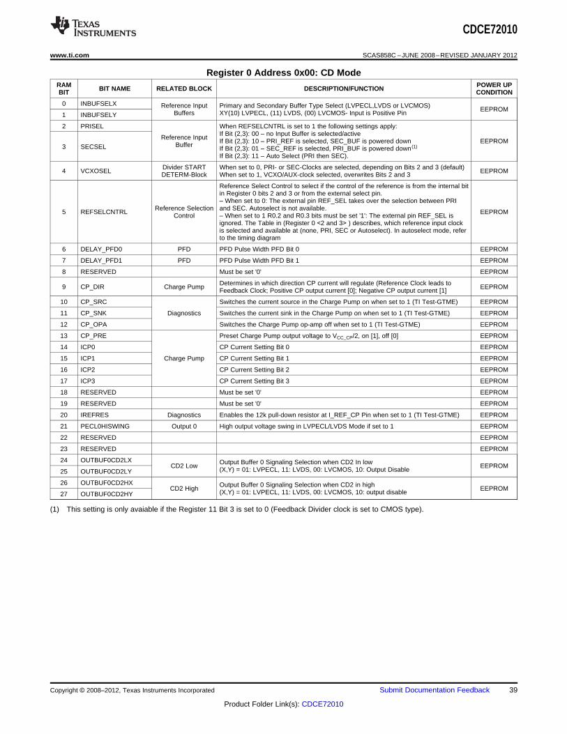
CDCE72010
www.ti.com SCAS858C –JUNE 2008–REVISED JANUARY 2012
Register 0 Address 0x00: CD ModeRAM POWER UPBIT NAME RELATED BLOCK DESCRIPTION/FUNCTIONBIT CONDITION
0 INBUFSELX Reference Input Primary and Secondary Buffer Type Select (LVPECL,LVDS or LVCMOS) EEPROMBuffers XY(10) LVPECL, (11) LVDS, (00) LVCMOS- Input is Positive Pin1 INBUFSELY
2 PRISEL When REFSELCNTRL is set to 1 the following settings apply:If Bit (2,3): 00 – no Input Buffer is selected/activeReference Input If Bit (2,3): 10 – PRI_REF is selected, SEC_BUF is powered down EEPROMBuffer3 SECSEL If Bit (2,3): 01 – SEC_REF is selected, PRI_BUF is powered down (1)
If Bit (2,3): 11 – Auto Select (PRI then SEC).
Divider START When set to 0, PRI- or SEC-Clocks are selected, depending on Bits 2 and 3 (default)4 VCXOSEL EEPROMDETERM-Block When set to 1, VCXO/AUX-clock selected, overwrites Bits 2 and 3
Reference Select Control to select if the control of the reference is from the internal bitin Register 0 bits 2 and 3 or from the external select pin.– When set to 0: The external pin REF_SEL takes over the selection between PRI
Reference Selection and SEC. Autoselect is not available.5 REFSELCNTRL EEPROMControl – When set to 1 R0.2 and R0.3 bits must be set '1': The external pin REF_SEL isignored. The Table in (Register 0 <2 and 3> ) describes, which reference input clockis selected and available at (none, PRI, SEC or Autoselect). In autoselect mode, referto the timing diagram
6 DELAY_PFD0 PFD PFD Pulse Width PFD Bit 0 EEPROM
7 DELAY_PFD1 PFD PFD Pulse Width PFD Bit 1 EEPROM
8 RESERVED Must be set '0' EEPROM
Determines in which direction CP current will regulate (Reference Clock leads to9 CP_DIR Charge Pump EEPROMFeedback Clock; Positive CP output current [0]; Negative CP output current [1]
10 CP_SRC Switches the current source in the Charge Pump on when set to 1 (TI Test-GTME) EEPROM
11 CP_SNK Diagnostics Switches the current sink in the Charge Pump on when set to 1 (TI Test-GTME) EEPROM
12 CP_OPA Switches the Charge Pump op-amp off when set to 1 (TI Test-GTME) EEPROM
13 CP_PRE Preset Charge Pump output voltage to VCC_CP/2, on [1], off [0] EEPROM
14 ICP0 CP Current Setting Bit 0 EEPROM
15 ICP1 Charge Pump CP Current Setting Bit 1 EEPROM
16 ICP2 CP Current Setting Bit 2 EEPROM
17 ICP3 CP Current Setting Bit 3 EEPROM
18 RESERVED Must be set '0' EEPROM
19 RESERVED Must be set '0' EEPROM
20 IREFRES Diagnostics Enables the 12k pull-down resistor at I_REF_CP Pin when set to 1 (TI Test-GTME) EEPROM
21 PECL0HISWING Output 0 High output voltage swing in LVPECL/LVDS Mode if set to 1 EEPROM
22 RESERVED EEPROM
23 RESERVED EEPROM
24 OUTBUF0CD2LX Output Buffer 0 Signaling Selection when CD2 In lowCD2 Low EEPROM(X,Y) = 01: LVPECL, 11: LVDS, 00: LVCMOS, 10: Output Disable25 OUTBUF0CD2LY
26 OUTBUF0CD2HX Output Buffer 0 Signaling Selection when CD2 in highCD2 High EEPROM(X,Y) = 01: LVPECL, 11: LVDS, 00: LVCMOS, 10: output disable27 OUTBUF0CD2HY
(1) This setting is only avaiable if the Register 11 Bit 3 is set to 0 (Feedback Divider clock is set to CMOS type).
Copyright © 2008–2012, Texas Instruments Incorporated Submit Documentation Feedback 39
Product Folder Link(s): CDCE72010
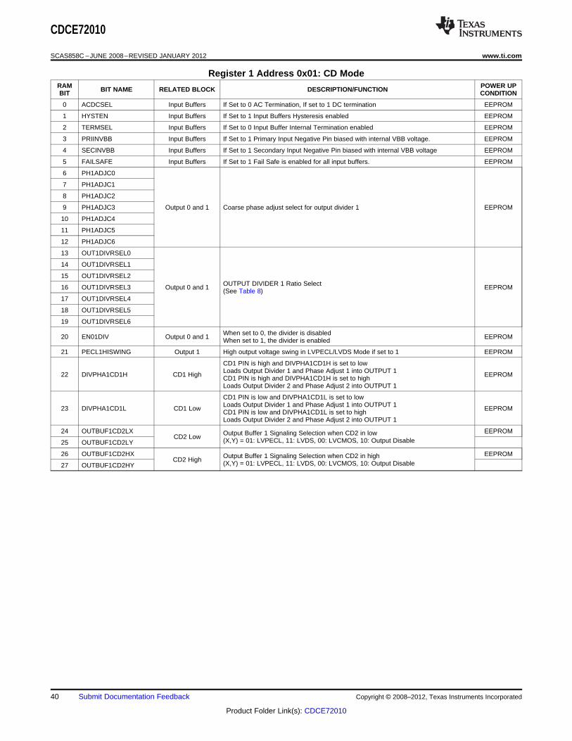
CDCE72010
SCAS858C –JUNE 2008–REVISED JANUARY 2012 www.ti.com
Register 1 Address 0x01: CD ModeRAM POWER UPBIT NAME RELATED BLOCK DESCRIPTION/FUNCTIONBIT CONDITION
0 ACDCSEL Input Buffers If Set to 0 AC Termination, If set to 1 DC termination EEPROM
1 HYSTEN Input Buffers If Set to 1 Input Buffers Hysteresis enabled EEPROM
2 TERMSEL Input Buffers If Set to 0 Input Buffer Internal Termination enabled EEPROM
3 PRIINVBB Input Buffers If Set to 1 Primary Input Negative Pin biased with internal VBB voltage. EEPROM
4 SECINVBB Input Buffers If Set to 1 Secondary Input Negative Pin biased with internal VBB voltage EEPROM
5 FAILSAFE Input Buffers If Set to 1 Fail Safe is enabled for all input buffers. EEPROM
6 PH1ADJC0
7 PH1ADJC1
8 PH1ADJC2
9 PH1ADJC3 Output 0 and 1 Coarse phase adjust select for output divider 1 EEPROM
10 PH1ADJC4
11 PH1ADJC5
12 PH1ADJC6
13 OUT1DIVRSEL0
14 OUT1DIVRSEL1
15 OUT1DIVRSEL2OUTPUT DIVIDER 1 Ratio Select16 OUT1DIVRSEL3 Output 0 and 1 EEPROM(See Table 8)
17 OUT1DIVRSEL4
18 OUT1DIVRSEL5
19 OUT1DIVRSEL6
When set to 0, the divider is disabled20 EN01DIV Output 0 and 1 EEPROMWhen set to 1, the divider is enabled
21 PECL1HISWING Output 1 High output voltage swing in LVPECL/LVDS Mode if set to 1 EEPROM
CD1 PIN is high and DIVPHA1CD1H is set to lowLoads Output Divider 1 and Phase Adjust 1 into OUTPUT 122 DIVPHA1CD1H CD1 High EEPROMCD1 PIN is high and DIVPHA1CD1H is set to highLoads Output Divider 2 and Phase Adjust 2 into OUTPUT 1
CD1 PIN is low and DIVPHA1CD1L is set to lowLoads Output Divider 1 and Phase Adjust 1 into OUTPUT 123 DIVPHA1CD1L CD1 Low EEPROMCD1 PIN is low and DIVPHA1CD1L is set to highLoads Output Divider 2 and Phase Adjust 2 into OUTPUT 1
24 OUTBUF1CD2LX EEPROMOutput Buffer 1 Signaling Selection when CD2 in lowCD2 Low (X,Y) = 01: LVPECL, 11: LVDS, 00: LVCMOS, 10: Output Disable25 OUTBUF1CD2LY
26 OUTBUF1CD2HX EEPROMOutput Buffer 1 Signaling Selection when CD2 in highCD2 High (X,Y) = 01: LVPECL, 11: LVDS, 00: LVCMOS, 10: Output Disable27 OUTBUF1CD2HY
40 Submit Documentation Feedback Copyright © 2008–2012, Texas Instruments Incorporated
Product Folder Link(s): CDCE72010
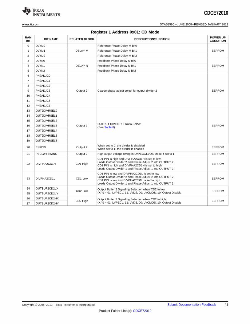
CDCE72010
www.ti.com SCAS858C –JUNE 2008–REVISED JANUARY 2012
Register 1 Address 0x01: CD ModeRAM POWER UPBIT NAME RELATED BLOCK DESCRIPTION/FUNCTIONBIT CONDITION
0 DLYM0 Reference Phase Delay M Bit0
1 DLYM1 DELAY M Reference Phase Delay M Bit1 EEPROM
2 DLYM2 Reference Phase Delay M Bit2
3 DLYN0 Feedback Phase Delay N Bit0
4 DLYN1 DELAY N Feedback Phase Delay N Bit1 EEPROM
5 DLYN2 Feedback Phase Delay N Bit2
6 PH2ADJC0
7 PH2ADJC1
8 PH2ADJC2
9 PH2ADJC3 Output 2 Coarse phase adjust select for output divider 2 EEPROM
10 PH2ADJC4
11 PH2ADJC5
12 PH2ADJC6
13 OUT2DIVRSEL0
14 OUT2DIVRSEL1
15 OUT2DIVRSEL2OUTPUT DIVIDER 2 Ratio Select16 OUT2DIVRSEL3 Output 2 EEPROM(See Table 8)
17 OUT2DIVRSEL4
18 OUT2DIVRSEL5
19 OUT2DIVRSEL6
When set to 0, the divider is disabled20 EN2DIV Output 2 EEPROMWhen set to 1, the divider is enabled
21 PECL2HISWING Output 2 High output voltage swing in LVPECL/LVDS Mode if set to 1 EEPROM
CD1 PIN is high and DIVPHA2CD1H is set to lowLoads Output Divider 2 and Phase Adjust 2 into OUTPUT 222 DIVPHA2CD1H CD1 High EEPROMCD1 PIN is high and DIVPHA2CD1H is set to highLoads Output Divider 1 and Phase Adjust 1 into OUTPUT 2
CD1 PIN is low and DIVPHA2CD1L is set to lowLoads Output Divider 2 and Phase Adjust 2 into OUTPUT 223 DIVPHA2CD1L CD1 Low EEPROMCD1 PIN is low and DIVPHA2CD1L is set to highLoads Output Divider 1 and Phase Adjust 1 into OUTPUT 2
24 OUTBUF2CD2LX Output Buffer 2 Signaling Selection when CD2 in lowCD2 Low EEPROM(X,Y) = 01: LVPECL, 11: LVDS, 00: LVCMOS, 10: Output Disable25 OUTBUF2CD2LY
26 OUTBUF2CD2HX Output Buffer 2 Signaling Selection when CD2 in highCD2 High EEPROM(X,Y) = 01: LVPECL, 11: LVDS, 00: LVCMOS, 10: Output Disable27 OUTBUF2CD2HY
Copyright © 2008–2012, Texas Instruments Incorporated Submit Documentation Feedback 41
Product Folder Link(s): CDCE72010
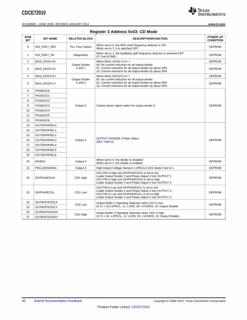
CDCE72010
SCAS858C –JUNE 2008–REVISED JANUARY 2012 www.ti.com
Register 3 Address 0x03: CD ModeRAM POWER UPBIT NAME RELATED BLOCK DESCRIPTION/FUNCTIONBIT CONDITION
When set to 0, the REF-clock frequency detector is ON0 DIS_FDET_REF PLL Freq. Detect EEPROMWhen set to 1, it is switched OFF
When set to 1, the feedback path frequency detector is switched OFF1 DIS_FDET_FB Diagnostics EEPROM(TI Test-GTME)
2 BIAS_DIV01<0> When BIAS_DIV01<1:0> = EEPROMOutput Divider 00, No current reduction for all output-divider
0 and 1 01, Current reduction for all output-divider by about 20%3 BIAS_DIV01<1> EEPROM10, Current reduction for all output-divider by about 30%
4 BIAS_DIV23<0> When BIAS_DIV23<1:0> = EEPROMOutput Divider 00, No current reduction for all output-divider
2 and 3 01, Current reduction for all output-divider by about 20%5 BIAS_DIV23<1> EEPROM10, Current reduction for all output-divider by about 30%
6 PH3ADJC0
7 PH3ADJC1
8 PH3ADJC2
9 PH3ADJC3 Output 3 Coarse phase adjust select for output divider 3 EEPROM
10 PH3ADJC4
11 PH3ADJC5
12 PH3ADJC6
13 OUT3DIVRSEL0
14 OUT3DIVRSEL1
15 OUT3DIVRSEL2OUTPUT DIVIDER 3 Ratio Select16 OUT3DIVRSEL3 Output 3 EEPROM(See Table 8)
17 OUT3DIVRSEL4
18 OUT3DIVRSEL5
19 OUT3DIVRSEL6
When set to 0, the divider is disabled20 EN3DIV Output 3 EEPROMWhen set to 1, the divider is enabled
21 PECL3HISWING Output 3 High Output Voltage Swing in LVPECL/LVDS Mode if set to 1 EEPROM
CD1 PIN is high and DIVPHA3CD1H is set to lowLoads Output Divider 3 and Phase Adjust 3 into OUTPUT 322 DIVPHA3CD1H CD1 High EEPROMCD1 PIN is high and DIVPHA3CD1H is set to highLoads Output Divider 4 and Phase Adjust 4 into OUTPUT 3
CD1 PIN is Low and DIVPHA3CD1L is set to lowLoads Output Divider 3 and Phase Adjust 3 into OUTPUT 323 DIVPHA3CD1L CD1 Low EEPROMCD1 PIN is Low and DIVPHA3CD1L is set to highLoads Output Divider 4 and Phase Adjust 4 into OUTPUT 3
24 OUTBUF3CD2LX Output Buffer 3 Signaling Selection when CD2 in lowCD2 Low EEPROM(X,Y) = 01:LVPECL, 11: LVDS, 00: LVCMOS, 10: Output Disable25 OUTBUF3CD2LY
26 OUTBUF3CD2HX Output Buffer 3 Signaling Selection when CD2 in highCD2 High EEPROM(X,Y) = 01: LVPECL, 11: LVDS, 00: LVCMOS, 10: Output Disable27 OUTBUF3CD2HY
42 Submit Documentation Feedback Copyright © 2008–2012, Texas Instruments Incorporated
Product Folder Link(s): CDCE72010
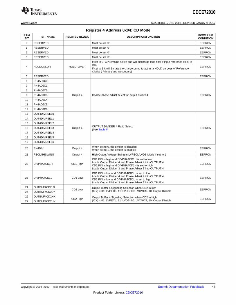
CDCE72010
www.ti.com SCAS858C –JUNE 2008–REVISED JANUARY 2012
Register 4 Address 0x04: CD ModeRAM POWER UPBIT NAME RELATED BLOCK DESCRIPTION/FUNCTIONBIT CONDITION
0 RESERVED Must be set '0' EEPROM
1 RESERVED Must be set '0' EEPROM
2 RESERVED Must be set '0' EEPROM
3 RESERVED Must be set '0' EEPROM
If set to 0, CP remains active and will discharge loop filter if input reference clock islost.
4 HOLDONLOR HOLD_OVER EEPROMIf set to 1 it will 3-state the charge pump to act as a HOLD on Loss of ReferenceClocks ( Primary and Secondary)
5 RESERVED EEPROM
6 PH4ADJC0
7 PH4ADJC1
8 PH4ADJC2
9 PH4ADJC3 Output 4 Coarse phase adjust select for output divider 4 EEPROM
10 PH4ADJC4
11 PH4ADJC5
12 PH4ADJC6
13 OUT4DIVRSEL0
14 OUT4DIVRSEL1
15 OUT4DIVRSEL2OUTPUT DIVIDER 4 Ratio Select16 OUT4DIVRSEL3 Output 4 EEPROM(See Table 8)
17 OUT4DIVRSEL4
18 OUT4DIVRSEL5
19 OUT4DIVRSEL6
When set to 0, the divider is disabled20 EN4DIV Output 4 EEPROMWhen set to 1, the divider is enabled
21 PECL4HISWING Output 4 High Output Voltage Swing in LVPECL/LVDS Mode if set to 1 EEPROM
CD1 PIN is high and DIVPHA4CD1H is set to lowLoads Output Divider 4 and Phase Adjust 4 into OUTPUT 422 DIVPHA4CD1H CD1 High EEPROMCD1 PIN is high and DIVPHA4CD1H is set to highLoads Output Divider 3 and Phase Adjust 3 into OUTPUT 4
CD1 PIN is low and DIVPHA4CD1L is set to lowLoads Output Divider 4 and Phase Adjust 4 into OUTPUT 423 DIVPHA4CD1L CD1 Low EEPROMCD1 PIN is low and DIVPHA4CD1L is set to highLoads Output Divider 3 and Phase Adjust 3 into OUTPUT 4
24 OUTBUF4CD2LX Output Buffer 4 Signaling Selection when CD2 in lowCD2 Low EEPROM(X,Y) = 01: LVPECL, 11: LVDS, 00: LVCMOS, 10: Output Disable25 OUTBUF4CD2LY
26 OUTBUF4CD2HX Output Buffer 4 Signaling Selection when CD2 in highCD2 High EEPROM(X,Y) = 01: LVPECL, 11: LVDS, 00: LVCMOS, 10: Output Disable27 OUTBUF4CD2HY
Copyright © 2008–2012, Texas Instruments Incorporated Submit Documentation Feedback 43
Product Folder Link(s): CDCE72010
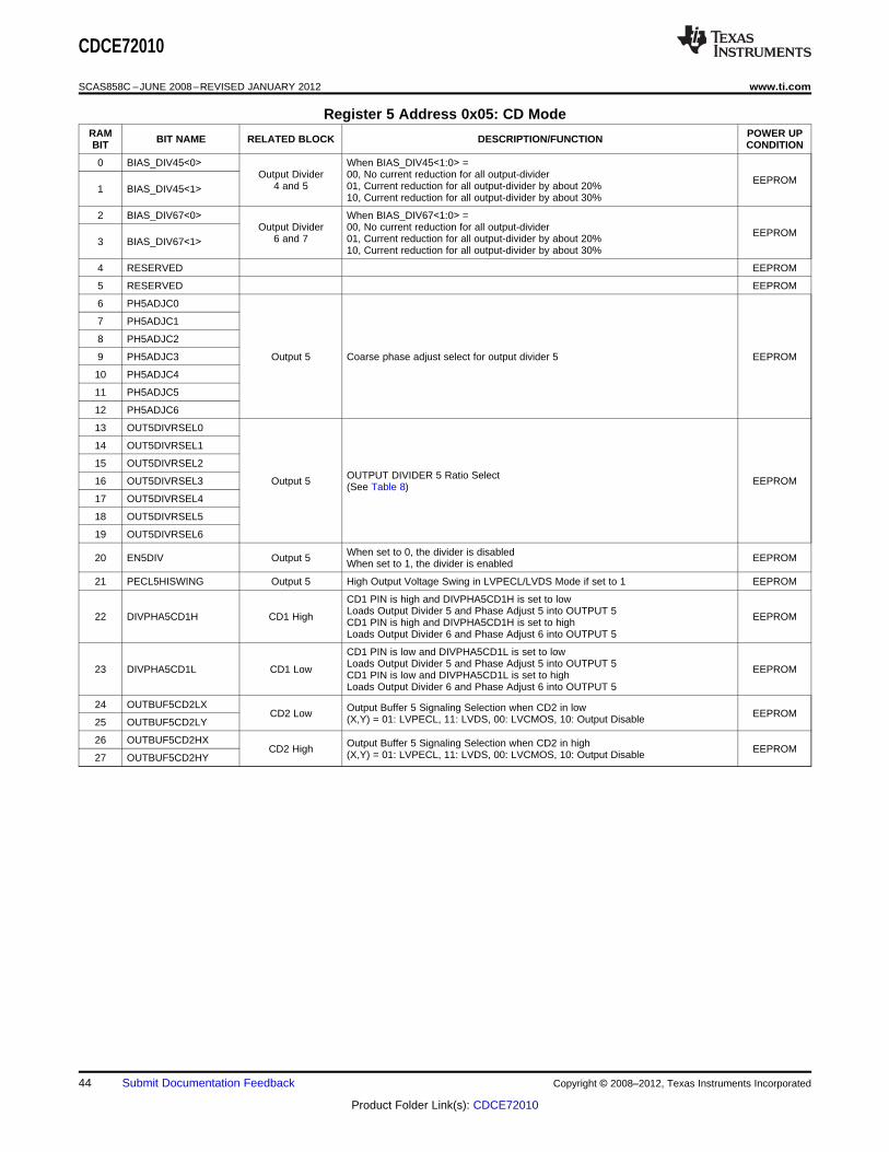
CDCE72010
SCAS858C –JUNE 2008–REVISED JANUARY 2012 www.ti.com
Register 5 Address 0x05: CD ModeRAM POWER UPBIT NAME RELATED BLOCK DESCRIPTION/FUNCTIONBIT CONDITION
0 BIAS_DIV45<0> When BIAS_DIV45<1:0> =Output Divider 00, No current reduction for all output-divider EEPROM4 and 5 01, Current reduction for all output-divider by about 20%1 BIAS_DIV45<1>
10, Current reduction for all output-divider by about 30%
2 BIAS_DIV67<0> When BIAS_DIV67<1:0> =Output Divider 00, No current reduction for all output-divider EEPROM6 and 7 01, Current reduction for all output-divider by about 20%3 BIAS_DIV67<1>
10, Current reduction for all output-divider by about 30%
4 RESERVED EEPROM
5 RESERVED EEPROM
6 PH5ADJC0
7 PH5ADJC1
8 PH5ADJC2
9 PH5ADJC3 Output 5 Coarse phase adjust select for output divider 5 EEPROM
10 PH5ADJC4
11 PH5ADJC5
12 PH5ADJC6
13 OUT5DIVRSEL0
14 OUT5DIVRSEL1
15 OUT5DIVRSEL2OUTPUT DIVIDER 5 Ratio Select16 OUT5DIVRSEL3 Output 5 EEPROM(See Table 8)
17 OUT5DIVRSEL4
18 OUT5DIVRSEL5
19 OUT5DIVRSEL6
When set to 0, the divider is disabled20 EN5DIV Output 5 EEPROMWhen set to 1, the divider is enabled
21 PECL5HISWING Output 5 High Output Voltage Swing in LVPECL/LVDS Mode if set to 1 EEPROM
CD1 PIN is high and DIVPHA5CD1H is set to lowLoads Output Divider 5 and Phase Adjust 5 into OUTPUT 522 DIVPHA5CD1H CD1 High EEPROMCD1 PIN is high and DIVPHA5CD1H is set to highLoads Output Divider 6 and Phase Adjust 6 into OUTPUT 5
CD1 PIN is low and DIVPHA5CD1L is set to lowLoads Output Divider 5 and Phase Adjust 5 into OUTPUT 523 DIVPHA5CD1L CD1 Low EEPROMCD1 PIN is low and DIVPHA5CD1L is set to highLoads Output Divider 6 and Phase Adjust 6 into OUTPUT 5
24 OUTBUF5CD2LX Output Buffer 5 Signaling Selection when CD2 in lowCD2 Low EEPROM(X,Y) = 01: LVPECL, 11: LVDS, 00: LVCMOS, 10: Output Disable25 OUTBUF5CD2LY
26 OUTBUF5CD2HX Output Buffer 5 Signaling Selection when CD2 in highCD2 High EEPROM(X,Y) = 01: LVPECL, 11: LVDS, 00: LVCMOS, 10: Output Disable27 OUTBUF5CD2HY
44 Submit Documentation Feedback Copyright © 2008–2012, Texas Instruments Incorporated
Product Folder Link(s): CDCE72010
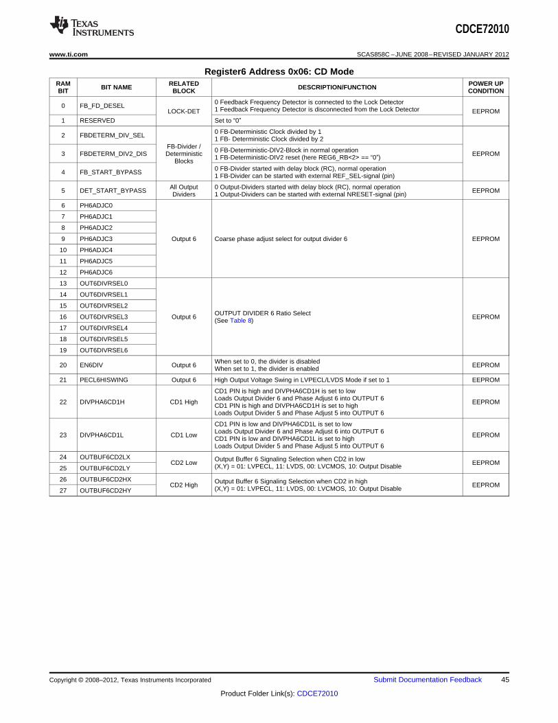
CDCE72010
www.ti.com SCAS858C –JUNE 2008–REVISED JANUARY 2012
Register6 Address 0x06: CD ModeRAM RELATED POWER UPBIT NAME DESCRIPTION/FUNCTIONBIT BLOCK CONDITION
0 Feedback Frequency Detector is connected to the Lock Detector0 FB_FD_DESEL 1 Feedback Frequency Detector is disconnected from the Lock DetectorLOCK-DET EEPROM1 RESERVED Set to “0”
0 FB-Deterministic Clock divided by 12 FBDETERM_DIV_SEL 1 FB- Deterministic Clock divided by 2FB-Divider / 0 FB-Deterministic-DIV2-Block in normal operation3 FBDETERM_DIV2_DIS Deterministic EEPROM1 FB-Deterministic-DIV2 reset (here REG6_RB<2> == “0”)Blocks
0 FB-Divider started with delay block (RC), normal operation4 FB_START_BYPASS 1 FB-Divider can be started with external REF_SEL-signal (pin)
All Output 0 Output-Dividers started with delay block (RC), normal operation5 DET_START_BYPASS EEPROMDividers 1 Output-Dividers can be started with external NRESET-signal (pin)
6 PH6ADJC0
7 PH6ADJC1
8 PH6ADJC2
9 PH6ADJC3 Output 6 Coarse phase adjust select for output divider 6 EEPROM
10 PH6ADJC4
11 PH6ADJC5
12 PH6ADJC6
13 OUT6DIVRSEL0
14 OUT6DIVRSEL1
15 OUT6DIVRSEL2OUTPUT DIVIDER 6 Ratio Select16 OUT6DIVRSEL3 Output 6 EEPROM(See Table 8)
17 OUT6DIVRSEL4
18 OUT6DIVRSEL5
19 OUT6DIVRSEL6
When set to 0, the divider is disabled20 EN6DIV Output 6 EEPROMWhen set to 1, the divider is enabled
21 PECL6HISWING Output 6 High Output Voltage Swing in LVPECL/LVDS Mode if set to 1 EEPROM
CD1 PIN is high and DIVPHA6CD1H is set to lowLoads Output Divider 6 and Phase Adjust 6 into OUTPUT 622 DIVPHA6CD1H CD1 High EEPROMCD1 PIN is high and DIVPHA6CD1H is set to highLoads Output Divider 5 and Phase Adjust 5 into OUTPUT 6
CD1 PIN is low and DIVPHA6CD1L is set to lowLoads Output Divider 6 and Phase Adjust 6 into OUTPUT 623 DIVPHA6CD1L CD1 Low EEPROMCD1 PIN is low and DIVPHA6CD1L is set to highLoads Output Divider 5 and Phase Adjust 5 into OUTPUT 6
24 OUTBUF6CD2LX Output Buffer 6 Signaling Selection when CD2 in lowCD2 Low EEPROM(X,Y) = 01: LVPECL, 11: LVDS, 00: LVCMOS, 10: Output Disable25 OUTBUF6CD2LY
26 OUTBUF6CD2HX Output Buffer 6 Signaling Selection when CD2 in highCD2 High EEPROM(X,Y) = 01: LVPECL, 11: LVDS, 00: LVCMOS, 10: Output Disable27 OUTBUF6CD2HY
Copyright © 2008–2012, Texas Instruments Incorporated Submit Documentation Feedback 45
Product Folder Link(s): CDCE72010
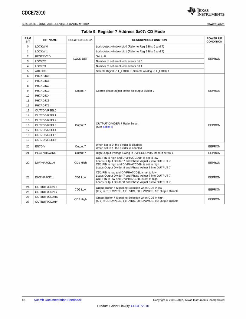
CDCE72010
SCAS858C –JUNE 2008–REVISED JANUARY 2012 www.ti.com
Table 9. Register 7 Address 0x07: CD Mode
RAM POWER UPBIT NAME RELATED BLOCK DESCRIPTION/FUNCTIONBIT CONDITION
0 LOCKW 0 Lock-detect window bit 0 (Refer to Reg 9 Bits 6 and 7)
1 LOCKW 1 Lock-detect window bit 1 (Refer to Reg 9 Bits 6 and 7)
2 RESERVED Set to 0LOCK-DET EEPROM
3 LOCKC0 Number of coherent lock events bit 0
4 LOCKC1 Number of coherent lock events bit 1
5 ADLOCK Selects Digital PLL_LOCK 0 ,Selects Analog PLL_LOCK 1
6 PH7ADJC0
7 PH7ADJC1
8 PH7ADJC2
9 PH7ADJC3 Output 7 Coarse phase adjust select for output divider 7 EEPROM
10 PH7ADJC4
11 PH7ADJC5
12 PH7ADJC6
13 OUT7DIVRSEL0
14 OUT7DIVRSEL1
15 OUT7DIVRSEL2OUTPUT DIVIDER 7 Ratio Select16 OUT7DIVRSEL3 Output 7 EEPROM(See Table 8)
17 OUT7DIVRSEL4
18 OUT7DIVRSEL5
19 OUT7DIVRSEL6
When set to 0, the divider is disabled20 EN7DIV Output 7 EEPROMWhen set to 1, the divider is enabled
21 PECL7HISWING Output 7 High Output Voltage Swing in LVPECL/LVDS Mode if set to 1 EEPROM
CD1 PIN is high and DIVPHA7CD1H is set to lowLoads Output Divider 7 and Phase Adjust 7 into OUTPUT 722 DIVPHA7CD1H CD1 High EEPROMCD1 PIN is high and DIVPHA7CD1H is set to highLoads Output Divider 8 and Phase Adjust 8 into OUTPUT 7
CD1 PIN is low and DIVPHA7CD1L is set to lowLoads Output Divider 7 and Phase Adjust 7 into OUTPUT 723 DIVPHA7CD1L CD1 Low EEPROMCD1 PIN is low and DIVPHA7CD1L is set to highLoads Output Divider 8 and Phase Adjust 8 into OUTPUT 7
24 OUTBUF7CD2LX Output Buffer 7 Signaling Selection when CD2 in lowCD2 Low EEPROM(X,Y) = 01: LVPECL, 11: LVDS, 00: LVCMOS, 10: Output Disable25 OUTBUF7CD2LY
26 OUTBUF7CD2HX Output Buffer 7 Signaling Selection when CD2 in highCD2 High EEPROM(X,Y) = 01: LVPECL, 11: LVDS, 00: LVCMOS, 10: Output Disable27 OUTBUF7CD2HY
46 Submit Documentation Feedback Copyright © 2008–2012, Texas Instruments Incorporated
Product Folder Link(s): CDCE72010
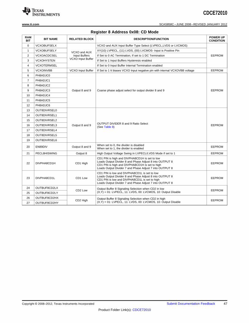
CDCE72010
www.ti.com SCAS858C –JUNE 2008–REVISED JANUARY 2012
Register 8 Address 0x08: CD ModeRAM POWER UPBIT NAME RELATED BLOCK DESCRIPTION/FUNCTIONBIT CONDITION
0 VCXOBUFSELX VCXO and AUX Input Buffer Type Select (LVPECL,LVDS or LVCMOS)
1 VCXOBUFSELY XY(10) LVPECL, (11) LVDS, (00) LVCMOS- Input is Positive PinVCXO and AUX
2 VCXOACDCSEL Input Buffers If Set to 0 AC Termination, If set to 1 DC Termination EEPROMVCXO Input Buffer
3 VCXOHYSTEN If Set to 1 Input Buffers Hysteresis enabled
4 VCXOTERMSEL If Set to 0 Input Buffer Internal Termination enabled
5 VCXOINVBB VCXO Input Buffer If Set to 1 It biases VCXO Input negative pin with internal VCXOVBB voltage EEPROM
6 PH8ADJC0
7 PH8ADJC1
8 PH8ADJC2
9 PH8ADJC3 Output 8 and 9 Coarse phase adjust select for output divider 8 and 9 EEPROM
10 PH8ADJC4
11 PH8ADJC5
12 PH8ADJC6
13 OUT8DIVRSEL0
14 OUT8DIVRSEL1
15 OUT8DIVRSEL2OUTPUT DIVIDER 8 and 9 Ratio Select16 OUT8DIVRSEL3 Output 8 and 9 EEPROM(See Table 8)
17 OUT8DIVRSEL4
18 OUT8DIVRSEL5
19 OUT8DIVRSEL6
When set to 0, the divider is disabled20 EN89DIV Output 8 and 9 EEPROMWhen set to 1, the divider is enabled
21 PECL8HISWING Output 8 High Output Voltage Swing in LVPECL/LVDS Mode if set to 1 EEPROM
CD1 PIN is high and DIVPHA8CD1H is set to lowLoads Output Divider 8 and Phase Adjust 8 into OUTPUT 822 DIVPHA8CD1H CD1 High EEPROMCD1 PIN is high and DIVPHA8CD1H is set to highLoads Output Divider 7 and Phase Adjust 7 into OUTPUT 8
CD1 PIN is low and DIVPHA8CD1L is set to lowLoads Output Divider 8 and Phase Adjust 8 into OUTPUT 823 DIVPHA8CD1L CD1 Low EEPROMCD1 PIN is low and DIVPHA8CD1L is set to highLoads Output Divider 7 and Phase Adjust 7 into OUTPUT 8
24 OUTBUF8CD2LX Output Buffer 8 Signaling Selection when CD2 in lowCD2 Low EEPROM(X,Y) = 01: LVPECL, 11: LVDS, 00: LVCMOS, 10: Output Disable25 OUTBUF8CD2LY
26 OUTBUF8CD2HX Output Buffer 8 Signaling Selection when CD2 in highCD2 High EEPROM(X,Y) = 01: LVPECL, 11: LVDS, 00: LVCMOS, 10: Output Disable27 OUTBUF8CD2HY
Copyright © 2008–2012, Texas Instruments Incorporated Submit Documentation Feedback 47
Product Folder Link(s): CDCE72010
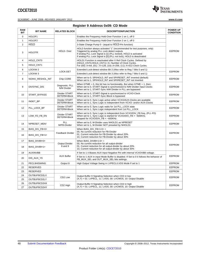
CDCE72010
SCAS858C –JUNE 2008–REVISED JANUARY 2012 www.ti.com
Register 9 Address 0x09: CD ModeRAM POWER UPBIT NAME RELATED BLOCK DESCRIPTION/FUNCTIONBIT CONDITION
0 HOLDF1 Enables the Frequency Hold-Over Function 1 on 1, off 0
1 HOLDF2 Enables the Frequency Hold-Over Function 2 on 1, off 0
2 HOLD 3-State Charge Pump 0 - (equal to HOLD-Pin function)
HOLD function always activated “1” (recommended for test purposes, only)HOLD- Over EEPROMTriggered by analog PLL Lock detect outputs3 HOLDTR If analog PLL Lock Signal is [1] (PLL locked), HOLD is activated
If analog PLL Lock Signal is [0] (PLL not lock), HOLD is deactivated
4 HOLD_CNT0 HOLD1 Function is reactivated after X Ref Clock Cycles. Defined by(HOLD_CNT0,HOLD_CNT1)::X= Number of Clock Cycles.
5 HOLD_CNT1 For (00)::X=64, (01) ::X=128, (10)::X=256, (11)::X=512 Clock Cycles.
6 LOCKW 2 Extended Lock-detect window Bit 2 (Also refer to Reg 7 Bits 0 and 1)LOCK-DET EEPROM
7 LOCKW 3 Extended Lock-detect window Bit 3 (Also refer to Reg 7 Bits 0 and 1)
When set to 0, SPI/HOLD_INT and SPI/RESET_INT inverted (default)8 NOINV_RESHOL_INT Chip CORE EEPROMWhen set to 1, SPI/HOLD_INT and SPI/RESET_INT not inverted
When GTME = 0, this bit has no functionality, But when GTME = 1, then:Diagnostic: PLL9 DIVSYNC_DIS When set to 0, START-Signal is synchronized to N/M Divider Input Clocks EEPROMN/M Divider When set to 1, START-Sync N/M Divider in PLL are bypassed
Divider START When set to 0, START-Signal is synchronized to VCXO-Clock10 START_BYPASS EEPROMDETERM-Block When set to 1, START-Sync Block is bypassed
Divider START When set to 0, Sync Logic active when VCXO/AUX-Clocks are available11 INDET_BP EEPROMDETERM-Block When set to 1, Sync Logic is independent from VCXO- and/or AUX-Clocks
Divider START When set to 0, Sync Logic waits for 1st PLL_LOCK state12 PLL_LOCK_BP EEPROMDETERM-Block When set to 1, Sync Logic independent from 1st PLL_LOCK
When set to 0, Sync Logic is independent from VCXO/DIV_FB freq. (PLL-FD)Divider START13 LOW_FD_FB_EN When set to 1, Sync Logic is started for VCXO/DIV_FB > ~600KHz, EEPROMDETERM-Block stopped for VCXO/DIV_FB < ~600KHz
PLL When set to 0, M-Divider uses NHOLD1 as NPRESET14 NPRESET_MDIV EEPROMM/FB-Divider When set to 1, M-Divider NOT preseted by NHOLD1
15 BIAS_DIV_FB<0> When BIAS_DIV_FB<1:0> =00, No current reduction for FB-DividerFeedback Divider EEPROM01, Current reduction for FB-Divider by about 20%16 BIAS_DIV_FB<1>10, Current reduction for FB-Divider by about 30%
17 BIAS_DIV89<0> When BIAS_DIV89<1:0> =Output Divider 00, No current reduction for all output-divider EEPROM8 and 9 01, Current reduction for all output-divider by about 20%18 BIAS_DIV89<1>
10, Current reduction for all output-divider by about 30%
19 AUXINVBB If Set to 1 it Biases AUX Input Negative Pin with internal VCXOVBB voltage.AUX Buffer EEPROMIf Set to 1 AUX in input Mode Buffer is disabled. If Set to 0 it follows the behavior of20 DIS_AUX_Y9 FB_MUX_SEL and OUT_MUX_SEL bits settings.
21 PECL9HISWING Output 9 High Output Voltage Swing in LVPECL/LVDS Mode if set to 1 EEPROM
22 RESERVED EEPROM
23 RESERVED EEPROM
24 OUTBUF9CD2LX Output Buffer 9 Signaling Selection when CD2 in lowCD2 Low EEPROM(X,Y) = 01: LVPECL, 11: LVDS, 00: LVCMOS, 10: Output Disable25 OUTBUF9CD2LY
26 OUTBUF9CD2HX Output Buffer 9 Signaling Selection when CD2 in highCD2 High EEPROM(X,Y) = 01: LVPECL, 11: LVDS, 00: LVCMOS, 10: Output Disable27 OUTBUF9CD2HY
48 Submit Documentation Feedback Copyright © 2008–2012, Texas Instruments Incorporated
Product Folder Link(s): CDCE72010
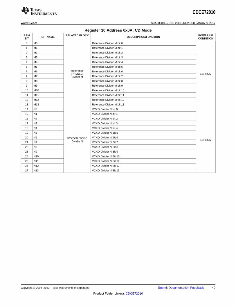
CDCE72010
www.ti.com SCAS858C –JUNE 2008–REVISED JANUARY 2012
Register 10 Address 0x0A: CD ModeRAM RELATED BLOCK POWER UPBIT NAME DESCRIPTION/FUNCTIONBIT CONDITION
0 M0 Reference Divider M bit 0
1 M1 Reference Divider M bit 1
2 M2 Reference Divider M bit 2
3 M3 Reference Divider M bit 3
4 M4 Reference Divider M bit 4
5 M5 Reference Divider M bit 5
Reference6 M6 Reference Divider M bit 6(PRI/SEC) EEPROM
7 M7 Reference Divider M bit 7Divider M
8 M8 Reference Divider M bit 8
9 M9 Reference Divider M bit 9
10 M10 Reference Divider M bit 10
11 M11 Reference Divider M bit 11
12 M12 Reference Divider M bit 12
13 M13 Reference Divider M bit 13
14 N0 VCXO Divider N bit 0
15 N1 VCXO Divider N bit 1
16 N2 VCXO Divider N bit 2
17 N3 VCXO Divider N bit 3
18 N4 VCXO Divider N bit 4
19 N5 VCXO Divider N Bit 5
20 N6 VCXO Divider N Bit 6VCXO/AUX/SEC EEPROMDivider N21 N7 VCXO Divider N Bit 7
22 N8 VCXO Divider N Bit 8
23 N9 VCXO Divider N Bit 9
24 N10 VCXO Divider N Bit 10
25 N11 VCXO Divider N Bit 11
26 N12 VCXO Divider N Bit 12
27 N13 VCXO Divider N Bit 13
Copyright © 2008–2012, Texas Instruments Incorporated Submit Documentation Feedback 49
Product Folder Link(s): CDCE72010
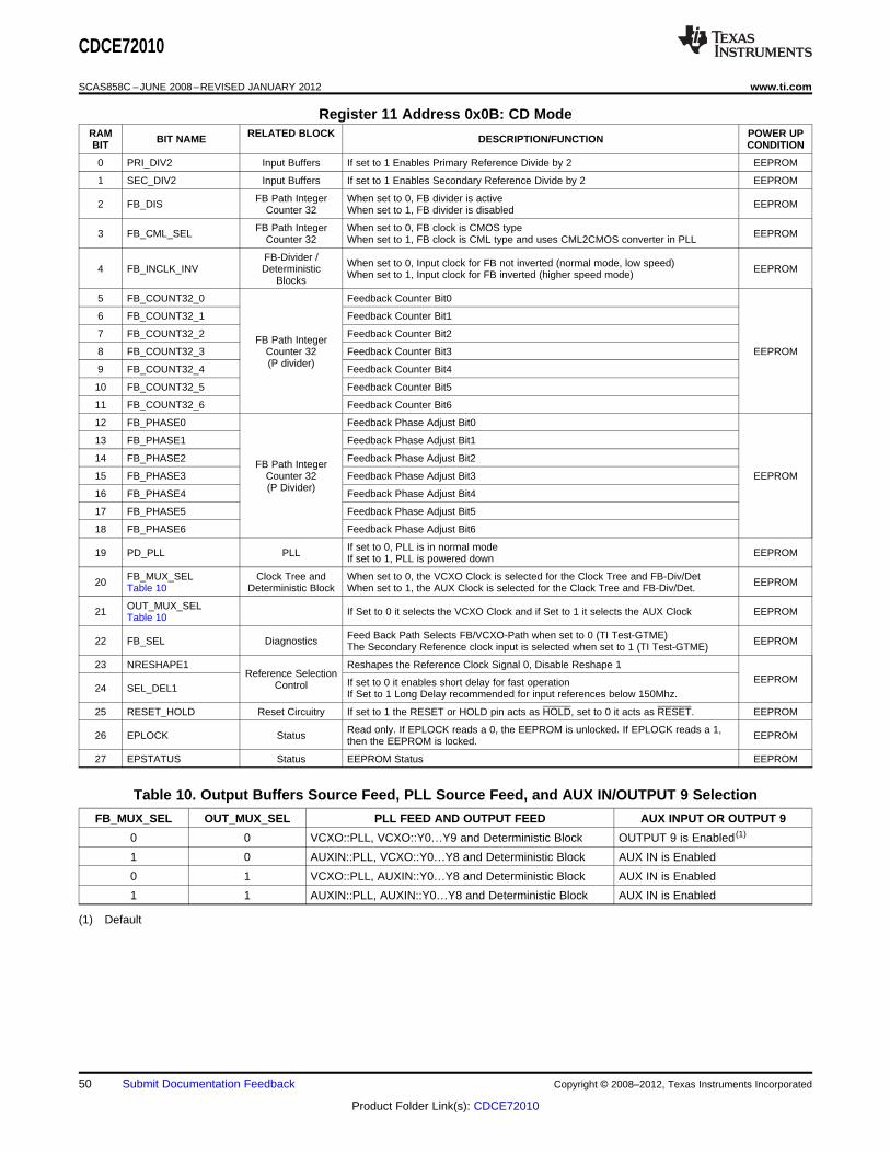
CDCE72010
SCAS858C –JUNE 2008–REVISED JANUARY 2012 www.ti.com
Register 11 Address 0x0B: CD ModeRAM RELATED BLOCK POWER UPBIT NAME DESCRIPTION/FUNCTIONBIT CONDITION
0 PRI_DIV2 Input Buffers If set to 1 Enables Primary Reference Divide by 2 EEPROM
1 SEC_DIV2 Input Buffers If set to 1 Enables Secondary Reference Divide by 2 EEPROM
FB Path Integer When set to 0, FB divider is active2 FB_DIS EEPROMCounter 32 When set to 1, FB divider is disabled
FB Path Integer When set to 0, FB clock is CMOS type3 FB_CML_SEL EEPROMCounter 32 When set to 1, FB clock is CML type and uses CML2CMOS converter in PLL
FB-Divider / When set to 0, Input clock for FB not inverted (normal mode, low speed)4 FB_INCLK_INV Deterministic EEPROMWhen set to 1, Input clock for FB inverted (higher speed mode)Blocks
5 FB_COUNT32_0 Feedback Counter Bit0
6 FB_COUNT32_1 Feedback Counter Bit1
7 FB_COUNT32_2 Feedback Counter Bit2FB Path Integer
8 FB_COUNT32_3 Counter 32 Feedback Counter Bit3 EEPROM(P divider)
9 FB_COUNT32_4 Feedback Counter Bit4
10 FB_COUNT32_5 Feedback Counter Bit5
11 FB_COUNT32_6 Feedback Counter Bit6
12 FB_PHASE0 Feedback Phase Adjust Bit0
13 FB_PHASE1 Feedback Phase Adjust Bit1
14 FB_PHASE2 Feedback Phase Adjust Bit2FB Path Integer
15 FB_PHASE3 Counter 32 Feedback Phase Adjust Bit3 EEPROM(P Divider)
16 FB_PHASE4 Feedback Phase Adjust Bit4
17 FB_PHASE5 Feedback Phase Adjust Bit5
18 FB_PHASE6 Feedback Phase Adjust Bit6
If set to 0, PLL is in normal mode19 PD_PLL PLL EEPROMIf set to 1, PLL is powered down
FB_MUX_SEL Clock Tree and When set to 0, the VCXO Clock is selected for the Clock Tree and FB-Div/Det20 EEPROMTable 10 Deterministic Block When set to 1, the AUX Clock is selected for the Clock Tree and FB-Div/Det.
OUT_MUX_SEL21 If Set to 0 it selects the VCXO Clock and if Set to 1 it selects the AUX Clock EEPROMTable 10
Feed Back Path Selects FB/VCXO-Path when set to 0 (TI Test-GTME)22 FB_SEL Diagnostics EEPROMThe Secondary Reference clock input is selected when set to 1 (TI Test-GTME)
23 NRESHAPE1 Reshapes the Reference Clock Signal 0, Disable Reshape 1Reference Selection EEPROMIf set to 0 it enables short delay for fast operationControl24 SEL_DEL1 If Set to 1 Long Delay recommended for input references below 150Mhz.
25 RESET_HOLD Reset Circuitry If set to 1 the RESET or HOLD pin acts as HOLD, set to 0 it acts as RESET. EEPROM
Read only. If EPLOCK reads a 0, the EEPROM is unlocked. If EPLOCK reads a 1,26 EPLOCK Status EEPROMthen the EEPROM is locked.
27 EPSTATUS Status EEPROM Status EEPROM
Table 10. Output Buffers Source Feed, PLL Source Feed, and AUX IN/OUTPUT 9 Selection
FB_MUX_SEL OUT_MUX_SEL PLL FEED AND OUTPUT FEED AUX INPUT OR OUTPUT 9
0 0 VCXO::PLL, VCXO::Y0…Y9 and Deterministic Block OUTPUT 9 is Enabled (1)
1 0 AUXIN::PLL, VCXO::Y0…Y8 and Deterministic Block AUX IN is Enabled
0 1 VCXO::PLL, AUXIN::Y0…Y8 and Deterministic Block AUX IN is Enabled
1 1 AUXIN::PLL, AUXIN::Y0…Y8 and Deterministic Block AUX IN is Enabled
(1) Default
50 Submit Documentation Feedback Copyright © 2008–2012, Texas Instruments Incorporated
Product Folder Link(s): CDCE72010
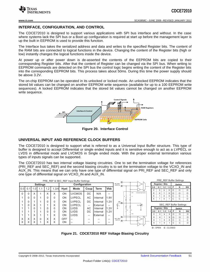
RAM Registers
EEPROM Cells
Interface & Control
Control Signals
SPI
--------ONXX1XXX
--------OFFXX0XXX
--External--LVDSONX11X11
1.2VInternalDCLVDSON001111
1.2VInternalACLVDSON001011
--External--LVPECLONX11X01
1.2VInternalDCLVPECLON001101
1.9VInternalACLVPECLON001001
--N/ADCLVCMOSONXX1X00
VbbTermCoupModeHyst1.3/41.21.11.00.10.0
ConfigurationSettings
OCC101X
CCC001X
OOOX1XX
OOOXX00
INVNP1.31.20.10.0
Register / Bits Switch
PRE_REF & SEC_REF Input Buffer Settings PRE_REF Buffer Settings
OCC101X
CCC001X
OOOX1XX
OOOXX00
INVNP1.41.20.10.0
Register / Bits Switch
SEC_REF Buffer Settings
O C- OPEN - CLOSED
Universal Input Control
N P
N P
INV
PRI_REF/
VCXO_IN
INV
SEC_REF/
AUX_IN
Vbb1 F
VBB
CDCE72010
www.ti.com SCAS858C –JUNE 2008–REVISED JANUARY 2012
INTERFACE, CONFIGURATION, AND CONTROL
The CDCE72010 is designed to support various applications with SPI bus interface and without. In the casewhere systems lack the SPI bus or a Boot up configuration is required at start up before the management layer isup the built in EEPROM is used to provide this function.
The Interface bus takes the serialized address and data and writes to the specified Register bits. The content ofthe RAM bits are connected to logical functions in the device. Changing the content of the Register bits (high orlow) instantly changes the logical functions inside the device.
At power up or after power down is de-asserted the contents of the EEPROM bits are copied to theircorresponding Register bits. After that the content of Register can be changed via the SPI bus. When writing toEEPROM commands are detected on the SPI bus the control logic begins writing the content of the Register bitsinto the corresponding EEPROM bits. This process takes about 50ms. During this time the power supply shouldbe above 3.2V.
The on-chip EEPROM can be operated in its unlocked or locked mode. An unlocked EEPROM indicates that thestored bit values can be changed on another EEPROM write sequence (available for up to a 100 EEPROM writesequences). A locked EEPROM indicates that the stored bit values cannot be changed on another EEPROMwrite sequence.
Figure 20. Interface Control
UNIVERSAL INPUT AND REFERENCE CLOCK BUFFERS
The CDCE72010 is designed to support what is referred to as a Universal Input Buffer structure. This type ofbuffer is designed to accept Differential or single ended inputs and it is sensitive enough to act as a LVPECL orLVDS in differential mode and LVCMOS in Single ended mode. With the proper external termination varioustypes of inputs signals can be supported.
The CDCE72010 has two internal voltage biasing circuitries. One to set the termination voltage for references(PRI_REF and SEC_REF) and the second biasing circuitry is to set the termination voltage to the VCXO_IN andAUX_IN. This means that we can only have one type of differential signal on PRI_REF and SEC_REF and onlyone type of differential signal on VCXO_IN and AUX_IN.
Figure 21. CDCE72010 REF Voltage Biasing Circuitry
Copyright © 2008–2012, Texas Instruments Incorporated Submit Documentation Feedback 51
Product Folder Link(s): CDCE72010
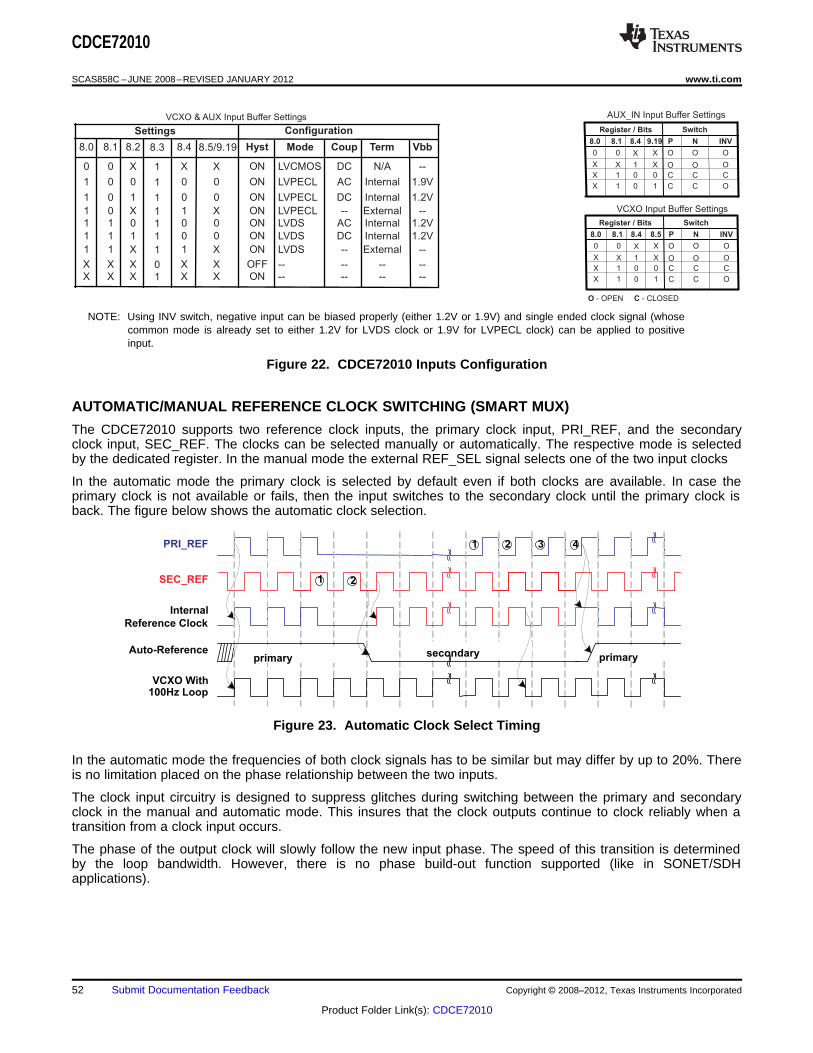
--------ONXX1XXX
--------OFFXX0XXX
--External--LVDSONX11X11
1.2VInternalDCLVDSON001111
1.2VInternalACLVDSON001011
--External--LVPECLONX11X01
1.2VInternalDCLVPECLON001101
1.9VInternalACLVPECLON001001
--N/ADCLVCMOSONXX1X00
VbbTermCoupModeHyst8.5/9.198.48.38.28.18.0
ConfigurationSettings
OCC101X
CCC001X
OOOX1XX
OOOXX00
INVNP9.198.48.18.0
Register / Bits Switch
VCXO & AUX Input Buffer Settings AUX_IN Input Buffer Settings
OCC101X
CCC001X
OOOX1XX
OOOXX00
INVNP8.58.48.18.0
Register / Bits Switch
VCXO Input Buffer Settings
O C- OPEN - CLOSED
PRI_REF
SEC_REF
Internal
Reference Clock
VCXO With100Hz Loop
Auto-Reference
1 2
1 2 3 4
primary secondary primary
CDCE72010
SCAS858C –JUNE 2008–REVISED JANUARY 2012 www.ti.com
NOTE: Using INV switch, negative input can be biased properly (either 1.2V or 1.9V) and single ended clock signal (whosecommon mode is already set to either 1.2V for LVDS clock or 1.9V for LVPECL clock) can be applied to positiveinput.
Figure 22. CDCE72010 Inputs Configuration
AUTOMATIC/MANUAL REFERENCE CLOCK SWITCHING (SMART MUX)
The CDCE72010 supports two reference clock inputs, the primary clock input, PRI_REF, and the secondaryclock input, SEC_REF. The clocks can be selected manually or automatically. The respective mode is selectedby the dedicated register. In the manual mode the external REF_SEL signal selects one of the two input clocks
In the automatic mode the primary clock is selected by default even if both clocks are available. In case theprimary clock is not available or fails, then the input switches to the secondary clock until the primary clock isback. The figure below shows the automatic clock selection.
Figure 23. Automatic Clock Select Timing
In the automatic mode the frequencies of both clock signals has to be similar but may differ by up to 20%. Thereis no limitation placed on the phase relationship between the two inputs.
The clock input circuitry is designed to suppress glitches during switching between the primary and secondaryclock in the manual and automatic mode. This insures that the clock outputs continue to clock reliably when atransition from a clock input occurs.
The phase of the output clock will slowly follow the new input phase. The speed of this transition is determinedby the loop bandwidth. However, there is no phase build-out function supported (like in SONET/SDHapplications).
52 Submit Documentation Feedback Copyright © 2008–2012, Texas Instruments Incorporated
Product Folder Link(s): CDCE72010
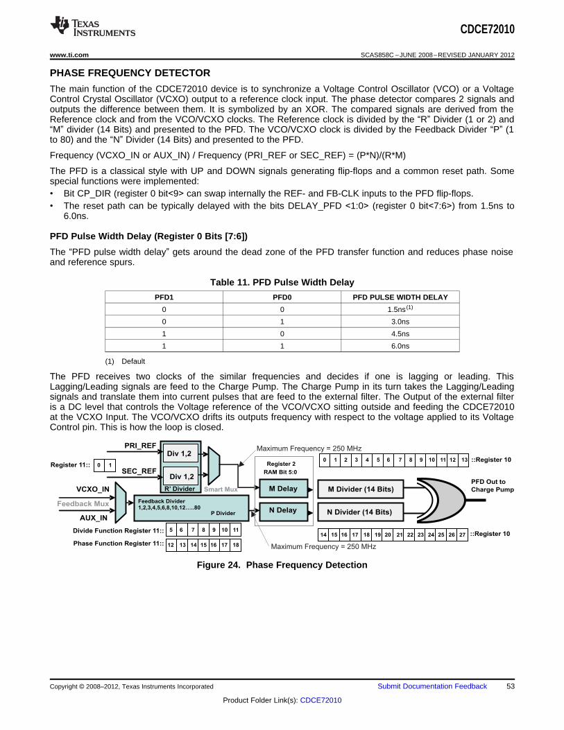
M Divider (14 Bits)
Feedback Divider1,2,3,4,5,6,8,10,12…..80
Smart Mux
Feedback Mux
PFD Out to
Charge Pump
P Divider
Div 1,2
Div 1,2
PRI_REF
SEC_REF
R’ Divider
Register 11::
Divide Function Register 11::
Phase Function Register 11:: 15
::Register 10
::Register 10
VCXO_IN
AUX_IN
M Delay
N Delay
Register 2
RAM Bit 5:0
14 16 17 181312
87 9 10 1165
N Divider (14 Bits)
0 1
15 16 17 1814
87 9 10 1165 131232 410
2221 23 24 252019 2726
Maximum Frequency = 250 MHz
Maximum Frequency = 250 MHz
CDCE72010
www.ti.com SCAS858C –JUNE 2008–REVISED JANUARY 2012
PHASE FREQUENCY DETECTOR
The main function of the CDCE72010 device is to synchronize a Voltage Control Oscillator (VCO) or a VoltageControl Crystal Oscillator (VCXO) output to a reference clock input. The phase detector compares 2 signals andoutputs the difference between them. It is symbolized by an XOR. The compared signals are derived from theReference clock and from the VCO/VCXO clocks. The Reference clock is divided by the “R” Divider (1 or 2) and“M” divider (14 Bits) and presented to the PFD. The VCO/VCXO clock is divided by the Feedback Divider “P” (1to 80) and the “N” Divider (14 Bits) and presented to the PFD.
Frequency (VCXO_IN or AUX_IN) / Frequency (PRI_REF or SEC_REF) = (P*N)/(R*M)
The PFD is a classical style with UP and DOWN signals generating flip-flops and a common reset path. Somespecial functions were implemented:• Bit CP_DIR (register 0 bit<9> can swap internally the REF- and FB-CLK inputs to the PFD flip-flops.• The reset path can be typically delayed with the bits DELAY_PFD <1:0> (register 0 bit<7:6>) from 1.5ns to
6.0ns.
PFD Pulse Width Delay (Register 0 Bits [7:6])
The “PFD pulse width delay” gets around the dead zone of the PFD transfer function and reduces phase noiseand reference spurs.
Table 11. PFD Pulse Width Delay
PFD1 PFD0 PFD PULSE WIDTH DELAY
0 0 1.5ns (1)
0 1 3.0ns
1 0 4.5ns
1 1 6.0ns
(1) Default
The PFD receives two clocks of the similar frequencies and decides if one is lagging or leading. ThisLagging/Leading signals are feed to the Charge Pump. The Charge Pump in its turn takes the Lagging/Leadingsignals and translate them into current pulses that are feed to the external filter. The Output of the external filteris a DC level that controls the Voltage reference of the VCO/VCXO sitting outside and feeding the CDCE72010at the VCXO Input. The VCO/VCXO drifts its outputs frequency with respect to the voltage applied to its VoltageControl pin. This is how the loop is closed.
Figure 24. Phase Frequency Detection
Copyright © 2008–2012, Texas Instruments Incorporated Submit Documentation Feedback 53
Product Folder Link(s): CDCE72010
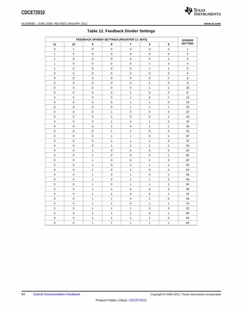
CDCE72010
SCAS858C –JUNE 2008–REVISED JANUARY 2012 www.ti.com
Table 12. Feedback Divider Settings
FEEDBACK DIVIDER SETTINGS (REGISTER 11: BITS) DIVIDERSETTING11 10 9 8 7 6 5
0 1 0 0 0 0 0 1
1 0 0 0 0 0 0 2
1 0 0 0 0 0 1 3
1 0 0 0 0 1 0 4
1 0 0 0 0 1 1 5
0 0 0 0 0 0 0 4'
0 0 0 0 0 0 1 6
0 0 0 0 0 1 0 8
0 0 0 0 0 1 1 10
0 0 0 0 1 0 0 8'
0 0 0 0 1 0 1 12
0 0 0 0 1 1 0 16
0 0 0 0 1 1 1 20
0 0 0 1 0 0 0 12'
0 0 0 1 0 0 1 18
0 0 0 1 0 1 0 24
0 0 0 1 0 1 1 30
0 0 0 1 1 0 0 16'
0 0 0 1 1 0 1 24'
0 0 0 1 1 1 0 32
0 0 0 1 1 1 1 40
0 0 1 0 0 0 0 20'
0 0 1 0 0 0 1 30'
0 0 1 0 0 1 0 40'
0 0 1 0 0 1 1 50
0 0 1 0 1 0 0 24'
0 0 1 0 1 0 1 36
0 0 1 0 1 1 0 48
0 0 1 0 1 1 1 60
0 0 1 1 0 0 0 28
0 0 1 1 0 0 1 42
0 0 1 1 0 1 0 56
0 0 1 1 0 1 1 70
0 0 1 1 1 0 0 32'
0 0 1 1 1 0 1 48'
0 0 1 1 1 1 0 64
0 0 1 1 1 1 1 80
54 Submit Documentation Feedback Copyright © 2008–2012, Texas Instruments Incorporated
Product Folder Link(s): CDCE72010
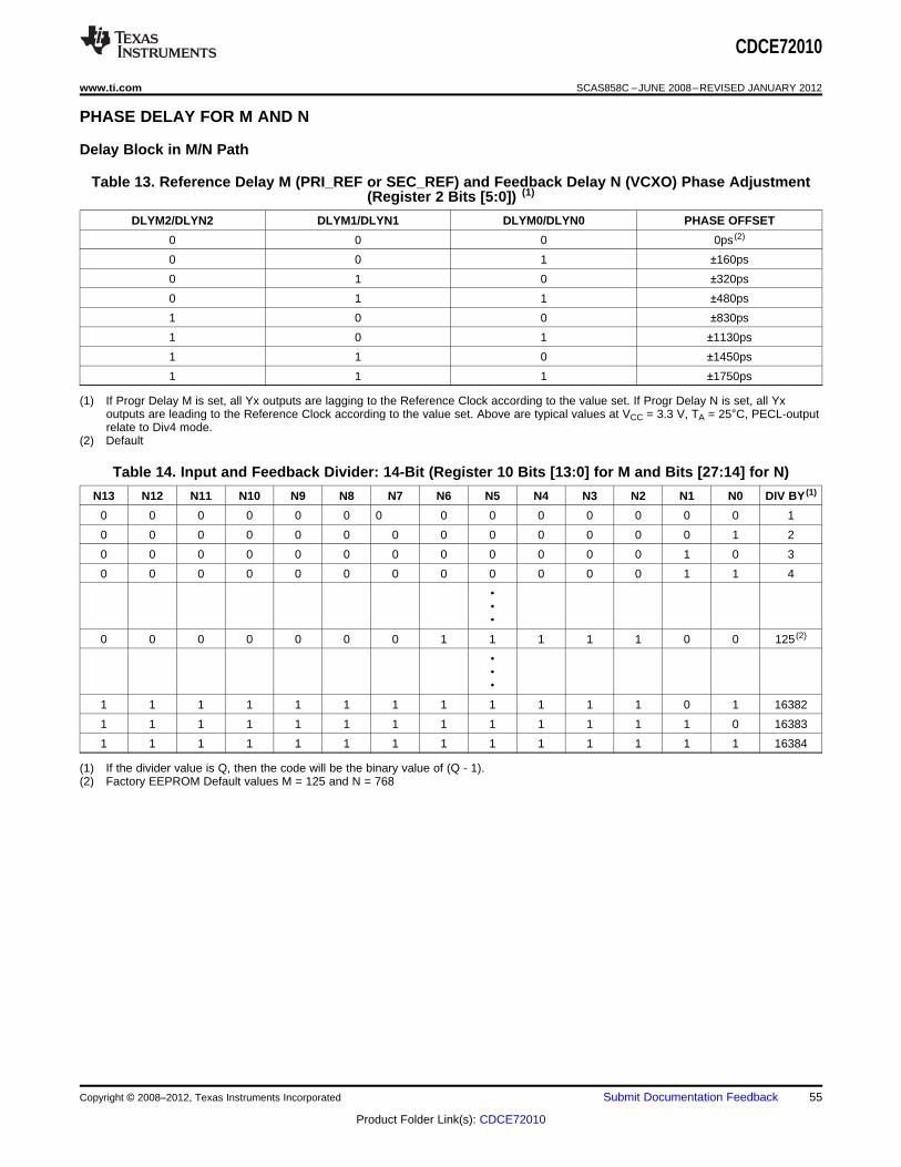
CDCE72010
www.ti.com SCAS858C –JUNE 2008–REVISED JANUARY 2012
PHASE DELAY FOR M AND N
Delay Block in M/N Path
Table 13. Reference Delay M (PRI_REF or SEC_REF) and Feedback Delay N (VCXO) Phase Adjustment(Register 2 Bits [5:0]) (1)
DLYM2/DLYN2 DLYM1/DLYN1 DLYM0/DLYN0 PHASE OFFSET
0 0 0 0ps (2)
0 0 1 ±160ps
0 1 0 ±320ps
0 1 1 ±480ps
1 0 0 ±830ps
1 0 1 ±1130ps
1 1 0 ±1450ps
1 1 1 ±1750ps
(1) If Progr Delay M is set, all Yx outputs are lagging to the Reference Clock according to the value set. If Progr Delay N is set, all Yxoutputs are leading to the Reference Clock according to the value set. Above are typical values at VCC = 3.3 V, TA = 25°C, PECL-outputrelate to Div4 mode.
(2) Default
Table 14. Input and Feedback Divider: 14-Bit (Register 10 Bits [13:0] for M and Bits [27:14] for N)
N13 N12 N11 N10 N9 N8 N7 N6 N5 N4 N3 N2 N1 N0 DIV BY (1)
0 0 0 0 0 0 0 0 0 0 0 0 0 0 1
0 0 0 0 0 0 0 0 0 0 0 0 0 1 2
0 0 0 0 0 0 0 0 0 0 0 0 1 0 3
0 0 0 0 0 0 0 0 0 0 0 0 1 1 4
•••
0 0 0 0 0 0 0 1 1 1 1 1 0 0 125 (2)
•••
1 1 1 1 1 1 1 1 1 1 1 1 0 1 16382
1 1 1 1 1 1 1 1 1 1 1 1 1 0 16383
1 1 1 1 1 1 1 1 1 1 1 1 1 1 16384
(1) If the divider value is Q, then the code will be the binary value of (Q - 1).(2) Factory EEPROM Default values M = 125 and N = 768
Copyright © 2008–2012, Texas Instruments Incorporated Submit Documentation Feedback 55
Product Folder Link(s): CDCE72010
CDCE72010
SCAS858C –JUNE 2008–REVISED JANUARY 2012 www.ti.com
CHARGE PUMP
The Charge Pump drives the loop filter that controls the external VCO/VCXO. The Charge pump operates at thePFD frequency since the function of the charge pump is to translate the UP DOWN signals of the PFD intocurrent pulses that drives the external filter. The Charge pump current is set by the control vector ICP [3:0].
Table 15. CP, Charge Pump Current (Register 0 RAM Bits [17:14])
TYPICAL CHARGE PUMPICP3 ICP2 ICP1 ICP0 CURRENT
0 0 0 0 0 μA (3-State)
0 0 0 1 200 μA
0 0 1 0 400 μA
0 0 1 1 600 μA
0 1 0 0 800 μA
0 1 0 1 1.0 mA
0 1 1 0 1.2 mA
0 1 1 1 1.4 mA
1 0 0 0 1.6 mA
1 0 0 1 1.8 mA
1 0 1 0 2.0 mA
1 0 1 1 2.2 mA (1)
1 1 0 0 2.4 mA
1 1 0 1 2.6 mA
1 1 1 0 2.8 mA
1 1 1 1 3.0 mA
(1) Default
The CP_PRE register bit R0.13 is a useful feature to quickly set the center frequency of the VC(X)O afterPower-up or Reset. The adequate control voltage for the VC(X)O will be provided to the Charge-Pump output byan internal voltage divider of 1KΩ/1KΩ to VCC_CP and GND (VCC_CP/2). The CP_PRE register bit must be reset to"0" in order for the PLL to achieve lock.
This feature helps to get the initial frequency accuracy, i.e. required at CPRI (Common Public Radio Interface) orOBSAI (Open Base Station Architecture Initiative).
The Preset Charge-Pump to VCC_CP/2 can be set and reset by register.
56 Submit Documentation Feedback Copyright © 2008–2012, Texas Instruments Incorporated
Product Folder Link(s): CDCE72010
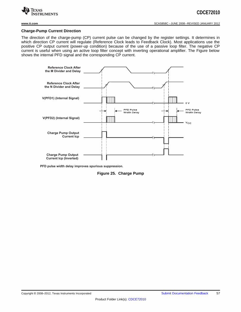
p .
V(PFD2) (Internal Signal)
V(PFD1) (Internal Signal)
Charge Pump OutputCurrent Icp
Charge Pump OutputCurrent Icp (Inverted)
Reference Clock Afterthe N Divider and Delay
Reference Clock Afterthe M Divider and Delay
PFD pulse width delay improves spurious suppression.
CDCE72010
www.ti.com SCAS858C –JUNE 2008–REVISED JANUARY 2012
Charge-Pump Current Direction
The direction of the charge-pump (CP) current pulse can be changed by the register settings. It determines inwhich direction CP current will regulate (Reference Clock leads to Feedback Clock). Most applications use thepositive CP output current (power-up condition) because of the use of a passive loop filter. The negative CPcurrent is useful when using an active loop filter concept with inverting operational amplifier. The Figure belowshows the internal PFD signal and the corresponding CP current.
Figure 25. Charge Pump
Copyright © 2008–2012, Texas Instruments Incorporated Submit Documentation Feedback 57
Product Folder Link(s): CDCE72010
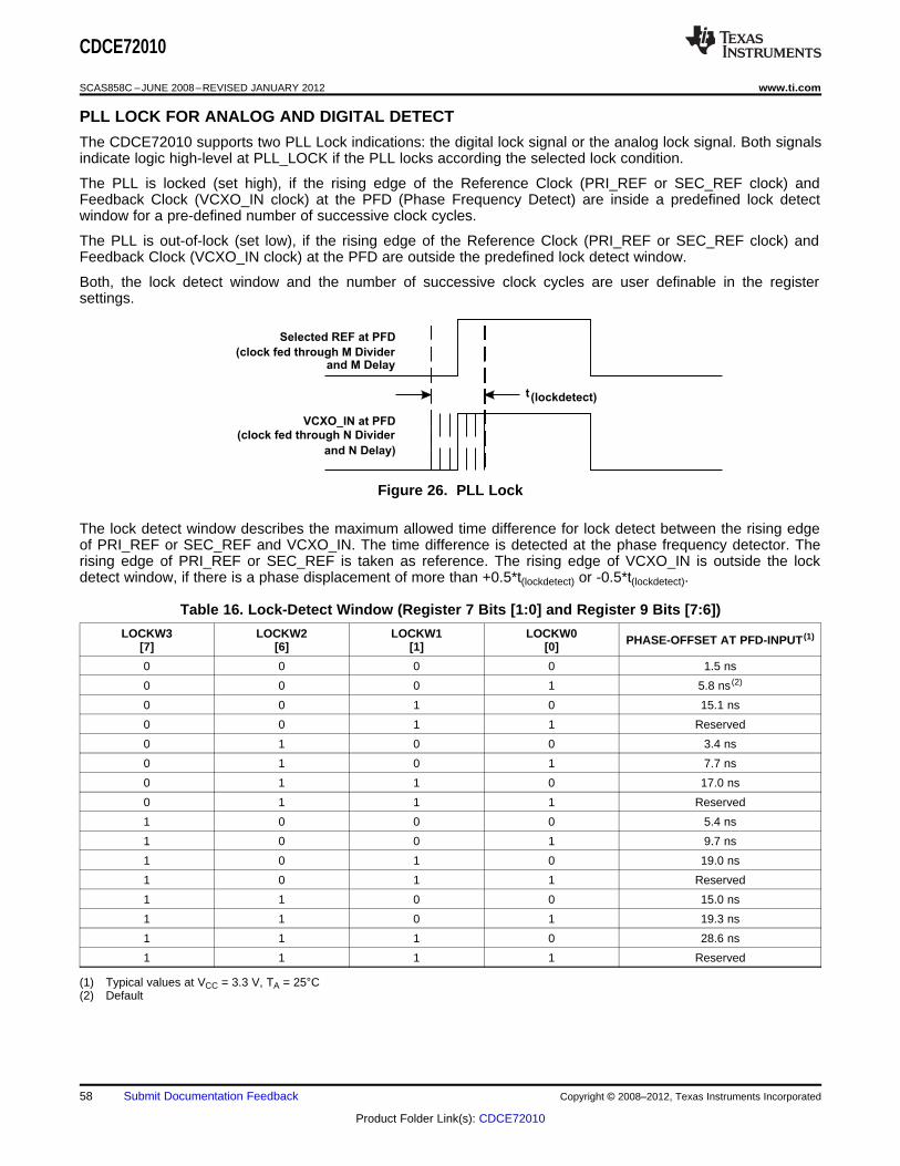
t (lockdetect)
Selected REF at PFD
(clock fed through M Dividerand M Delay
VCXO_IN at PFD
(clock fed through N Divider
and N Delay)
CDCE72010
SCAS858C –JUNE 2008–REVISED JANUARY 2012 www.ti.com
PLL LOCK FOR ANALOG AND DIGITAL DETECT
The CDCE72010 supports two PLL Lock indications: the digital lock signal or the analog lock signal. Both signalsindicate logic high-level at PLL_LOCK if the PLL locks according the selected lock condition.
The PLL is locked (set high), if the rising edge of the Reference Clock (PRI_REF or SEC_REF clock) andFeedback Clock (VCXO_IN clock) at the PFD (Phase Frequency Detect) are inside a predefined lock detectwindow for a pre-defined number of successive clock cycles.
The PLL is out-of-lock (set low), if the rising edge of the Reference Clock (PRI_REF or SEC_REF clock) andFeedback Clock (VCXO_IN clock) at the PFD are outside the predefined lock detect window.
Both, the lock detect window and the number of successive clock cycles are user definable in the registersettings.
Figure 26. PLL Lock
The lock detect window describes the maximum allowed time difference for lock detect between the rising edgeof PRI_REF or SEC_REF and VCXO_IN. The time difference is detected at the phase frequency detector. Therising edge of PRI_REF or SEC_REF is taken as reference. The rising edge of VCXO_IN is outside the lockdetect window, if there is a phase displacement of more than +0.5*t(lockdetect) or -0.5*t(lockdetect).
Table 16. Lock-Detect Window (Register 7 Bits [1:0] and Register 9 Bits [7:6])
LOCKW3 LOCKW2 LOCKW1 LOCKW0 PHASE-OFFSET AT PFD-INPUT (1)[7] [6] [1] [0]
0 0 0 0 1.5 ns
0 0 0 1 5.8 ns (2)
0 0 1 0 15.1 ns
0 0 1 1 Reserved
0 1 0 0 3.4 ns
0 1 0 1 7.7 ns
0 1 1 0 17.0 ns
0 1 1 1 Reserved
1 0 0 0 5.4 ns
1 0 0 1 9.7 ns
1 0 1 0 19.0 ns
1 0 1 1 Reserved
1 1 0 0 15.0 ns
1 1 0 1 19.3 ns
1 1 1 0 28.6 ns
1 1 1 1 Reserved
(1) Typical values at VCC = 3.3 V, TA = 25°C(2) Default
58 Submit Documentation Feedback Copyright © 2008–2012, Texas Instruments Incorporated
Product Folder Link(s): CDCE72010
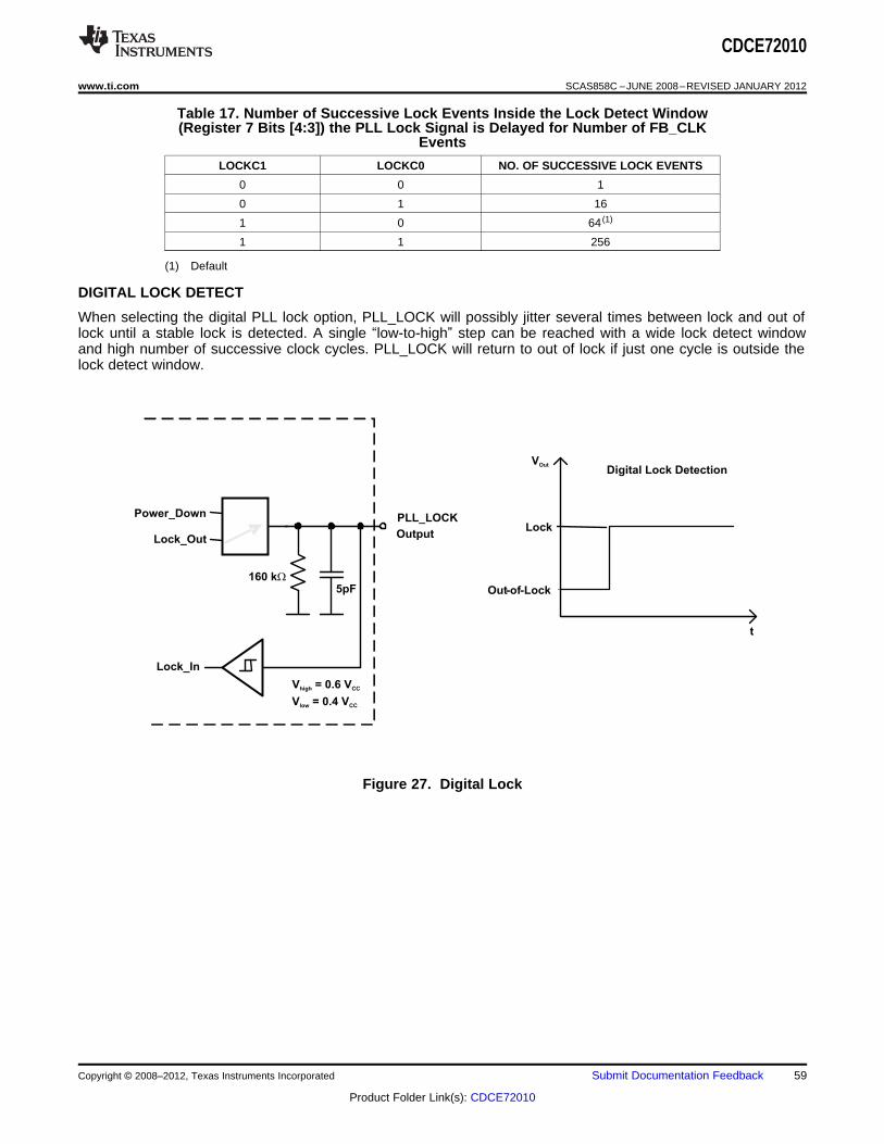
Power_Down
Lock_Out
Lock_In
160 kW
5pF
PLL_LOCK
Output
V = 0.6 Vhigh CC
V = 0.4 Vlow CC
Lock
t
Digital Lock Detection
Out-of-Lock
VOut
CDCE72010
www.ti.com SCAS858C –JUNE 2008–REVISED JANUARY 2012
Table 17. Number of Successive Lock Events Inside the Lock Detect Window(Register 7 Bits [4:3]) the PLL Lock Signal is Delayed for Number of FB_CLK
Events
LOCKC1 LOCKC0 NO. OF SUCCESSIVE LOCK EVENTS
0 0 1
0 1 16
1 0 64 (1)
1 1 256
(1) Default
DIGITAL LOCK DETECT
When selecting the digital PLL lock option, PLL_LOCK will possibly jitter several times between lock and out oflock until a stable lock is detected. A single “low-to-high” step can be reached with a wide lock detect windowand high number of successive clock cycles. PLL_LOCK will return to out of lock if just one cycle is outside thelock detect window.
Figure 27. Digital Lock
Copyright © 2008–2012, Texas Instruments Incorporated Submit Documentation Feedback 59
Product Folder Link(s): CDCE72010
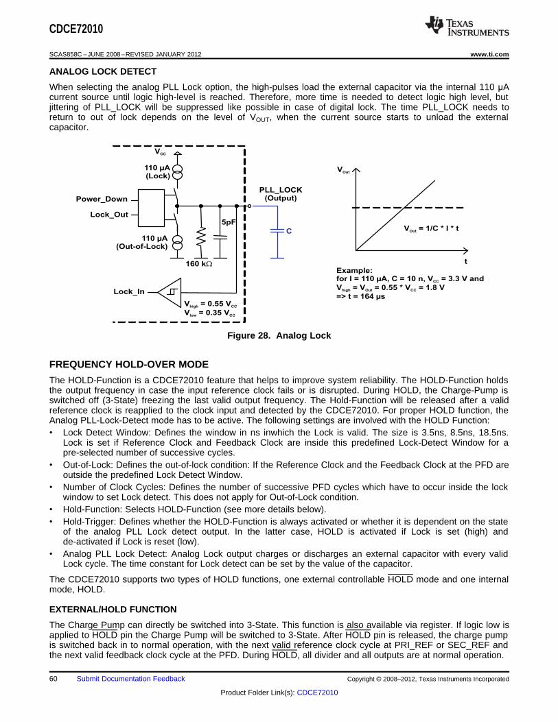
160 kW
5pF
110 µA(Lock)
VCC
C
VOut
t
V = 1/C * I * tOut
V = 0.55 Vhigh CC
V = 0.35 Vlow CC
Example:for I = 110 µA, C = 10 n, V = 3.3 V and
V = V = 0.55 * V = 1.8 V
=> t = 164 µs
CC
high Out CC
Power_Down
110 µA(Out-of-Lock)
Lock_Out
Lock_In
PLL_LOCK(Output)
CDCE72010
SCAS858C –JUNE 2008–REVISED JANUARY 2012 www.ti.com
ANALOG LOCK DETECT
When selecting the analog PLL Lock option, the high-pulses load the external capacitor via the internal 110 μAcurrent source until logic high-level is reached. Therefore, more time is needed to detect logic high level, butjittering of PLL_LOCK will be suppressed like possible in case of digital lock. The time PLL_LOCK needs toreturn to out of lock depends on the level of VOUT, when the current source starts to unload the externalcapacitor.
Figure 28. Analog Lock
FREQUENCY HOLD-OVER MODE
The HOLD-Function is a CDCE72010 feature that helps to improve system reliability. The HOLD-Function holdsthe output frequency in case the input reference clock fails or is disrupted. During HOLD, the Charge-Pump isswitched off (3-State) freezing the last valid output frequency. The Hold-Function will be released after a validreference clock is reapplied to the clock input and detected by the CDCE72010. For proper HOLD function, theAnalog PLL-Lock-Detect mode has to be active. The following settings are involved with the HOLD Function:• Lock Detect Window: Defines the window in ns inwhich the Lock is valid. The size is 3.5ns, 8.5ns, 18.5ns.
Lock is set if Reference Clock and Feedback Clock are inside this predefined Lock-Detect Window for apre-selected number of successive cycles.
• Out-of-Lock: Defines the out-of-lock condition: If the Reference Clock and the Feedback Clock at the PFD areoutside the predefined Lock Detect Window.
• Number of Clock Cycles: Defines the number of successive PFD cycles which have to occur inside the lockwindow to set Lock detect. This does not apply for Out-of-Lock condition.
• Hold-Function: Selects HOLD-Function (see more details below).• Hold-Trigger: Defines whether the HOLD-Function is always activated or whether it is dependent on the state
of the analog PLL Lock detect output. In the latter case, HOLD is activated if Lock is set (high) andde-activated if Lock is reset (low).
• Analog PLL Lock Detect: Analog Lock output charges or discharges an external capacitor with every validLock cycle. The time constant for Lock detect can be set by the value of the capacitor.
The CDCE72010 supports two types of HOLD functions, one external controllable HOLD mode and one internalmode, HOLD.
EXTERNAL/HOLD FUNCTION
The Charge Pump can directly be switched into 3-State. This function is also available via register. If logic low isapplied to HOLD pin the Charge Pump will be switched to 3-State. After HOLD pin is released, the charge pumpis switched back in to normal operation, with the next valid reference clock cycle at PRI_REF or SEC_REF andthe next valid feedback clock cycle at the PFD. During HOLD, all divider and all outputs are at normal operation.
60 Submit Documentation Feedback Copyright © 2008–2012, Texas Instruments Incorporated
Product Folder Link(s): CDCE72010
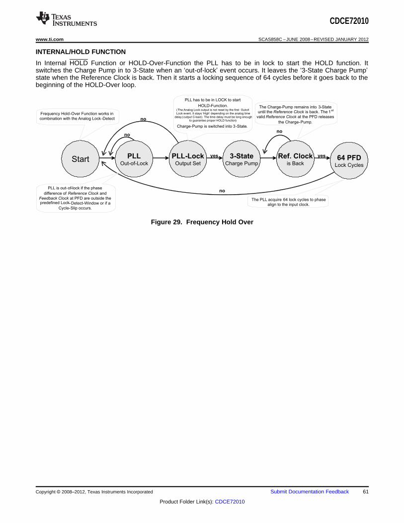
3-StateCharge Pump
yes yes
no
PLLOut-of-Lock
PLL-LockOutput Set
no
64 PFDLock Cycles
Ref. Clockis Back
no
no
Start
PLL is out-of-lock if the phase
difference of Reference Clock and
Feedback Clock at PFD are outside thepredefined Lock-Detect-Window or if a
Cycle-Slip occurs.
Frequency Hold-Over Function works in
combination with the Analog Lock -Detect
Charge-Pump is switched into 3-State.
PLL has to be in LOCK to start
HOLD-Function.(The Analog Lock output is not reset by the first Out-of-
Lock event. It stays ‘High’ depending on the analog time
delay (output C-load). The time delay must be long enoughto guarantee proper HOLD function)
The Charge-Pump remains into 3-Stateuntil the Reference Clock is back. The 1st
valid Reference Clock at the PFD releases
the Charge-Pump.
The PLL acquire 64 lock cycles to phase
align to the input clock.
CDCE72010
www.ti.com SCAS858C –JUNE 2008–REVISED JANUARY 2012
INTERNAL/HOLD FUNCTION
In Internal HOLD Function or HOLD-Over-Function the PLL has to be in lock to start the HOLD function. Itswitches the Charge Pump in to 3-State when an ‘out-of-lock’ event occurs. It leaves the ‘3-State Charge Pump’state when the Reference Clock is back. Then it starts a locking sequence of 64 cycles before it goes back to thebeginning of the HOLD-Over loop.
Figure 29. Frequency Hold Over
Copyright © 2008–2012, Texas Instruments Incorporated Submit Documentation Feedback 61
Product Folder Link(s): CDCE72010
D D D D D
Start Divider
(OUT#DIVSEL#)
(PH#ADJC#)
Output Divider
Coarse Phase Adjust Select
Phase Adjust Period
CDCE72010
SCAS858C –JUNE 2008–REVISED JANUARY 2012 www.ti.com
OUTPUT DIVIDERS AND PHASE ADJUST
The CDCE72010 is designed with individual Output Dividers for Outputs 1 to 8. Output Divider 1 drives Output 1and Output 0 and Output Divider 8 drives Output 8 and Output 9. Each output divider has a bypass function or itis referred to as divide by “one”. Since divide by one bypasses the divider block it can address higher operatingfrequencies.
The output divider is designed to address divide by 1, 2, 3, 4, 5, 6, 8, 10, 12, 16, 18, 20, 24, 28, 30, 32, 36, 40,42, 48, 50, 56, 60, 64, 70 and 80.The output divider includes a coarse phase adjust that shifts the divided clocksignal. The phase adjust resolution is a function of the divide function. The maximum number of phase stepsequals to the divider setting.
If the output is divide by 2, then two phase adjustment settings (0 and 180 degrees) are available. The resolutionof phase adjustment is related to the output divider setting by the following: Phase adjust resolution = (1/OutputDivider settings) X 360 Degrees.
Example: For a 491.52MHz VCXO where one of the outputs of the device is set to divide by 16 for a 30.72MHzdesired output, this will mean that the 30.72MHz clock will have (1/16) X 360 = 22.5 Degrees of phaseadjustment resolution.
Output Divide Select (OUT#DIVSEL#) and Coarse Phase Adjust Select (PH#ADJC#) registers are located inRegister 1 thought 8 for Output 1 thought 8 respectively.
The Phase difference between 2 divider settings on different output can be calculated using the following formulaand referring to the Phase Lag number in the Output Divider Table ( see Table 8).
Integer Remainder of [(Phase Lag X - Phase Lag Y)/ Divide X ] as an example if we need to calculate the phasedifference between divide by 4 and divide by 8 with respect to divide by 4 clock.
The Integer Remainder [(28.5 - 0.5)/4] = 0. This means there is 0 Cycle phase delay between Divide by 4 andDivide by 8 with respect to Divide by 4 Clock.
If we need to do the same calculation with respect to Divide by 8 we will have Intger Remainder [(28.5 – 0.5)/8] =0.5 that means that there is 0.5 Cycles between Divide by 4 and divide by 8 with respect to a divide by 8 clock.
Figure 30. Maximum Output Frequency With Phase Alighment
FREQUENCY DETECTION CIRCUIT
The Frequency detector circuit can detect the input clock signal and provide the indications at STATUS pindepending on Register 12 and 3 settings (see notes in page 33). The STATUS pin will set to HIGH if a valid inputclock is detected. And LOW if valid input clock is absent or missing.
The frequency detector circuit is located in between the SMART MUX and the M divider (see Figure 31).
62 Submit Documentation Feedback Copyright © 2008–2012, Texas Instruments Incorporated
Product Folder Link(s): CDCE72010
STATUS PIN
SEC_ REF
PRI_ REF
M divider
Smart MUX FREQ_DET
R’
R’ PFD
N divider
CDCE72010
www.ti.com SCAS858C –JUNE 2008–REVISED JANUARY 2012
Figure 31. Location of the Frequency Detector Circuit
The detection circuit is RC-based analog circuit. The response time to detect a new clock signal isclock-frequency dependent (min. 3.125µs at 0.8MHz). With higher clock frequency the response time will befaster as well.
If the input clock goes away, the detector reports the event within 5.2 µs independent of clock frequency.
Table 18. Specifications
PARAMETER MIN TYP MAX UNIT
Frequency detection threshold (1) 800 kHz
Response time (clock absence) (1) 2.62 5.2 µs
Response time (clock resumes) at 0.8 MHz (1) 3.125 29 µs
Clock cycles (clock resumes) at 0.8 MHz (2) 2.5 23 cycles
(1) Received values from simulation(2) Received values from simulation
Copyright © 2008–2012, Texas Instruments Incorporated Submit Documentation Feedback 63
Product Folder Link(s): CDCE72010
Only one side of the pin pads is shown.
Only two capacitors are illustrated.
Top Side Thermal PAD Layout
Bottom Side Thermal PAD Layout
Only two capacitors are illustrated.
CDCE72010
SCAS858C –JUNE 2008–REVISED JANUARY 2012 www.ti.com
DEVICE LAYOUT
The CDCE72010 is a high performance device packaged in a QFN-64. The die has all the ground pins boundedto the thermal PAD on the bottom of the package. Therefore it is essential that the connection from the thermalPAD to the ground layers should be low impedance. In addition, the thermal path in a QFN package is via thethermal PAD on the bottom of the package. Therefore, the layout of the PAD is very important and it will affectthe thermal performance as well as the overall performance of the device. The illustration shown providesoptimal performance in terms of thermal issues, inductance and power supply bypassing. The 10 X 10 Filled VIApattern recommended allows for a low inductance connection between the thermal ground pad and the groundplane of the board. This pattern forms a low thermal resistive path for the heat generated by the die to getdissipated through the ground plane and to the exposed bottom side ground pad. It is recommended that soldermask not be used on this bottom side pad to maximize its effectiveness as a thermal heat sink. Therecommended layout drives the thermal conductivity to 22.8 C°/W in still air and 13.8 C°/W in a 100LFM air flowif implemented on a JEDEC compliant test thermal board.
Figure 32. Device Layout
64 Submit Documentation Feedback Copyright © 2008–2012, Texas Instruments Incorporated
Product Folder Link(s): CDCE72010
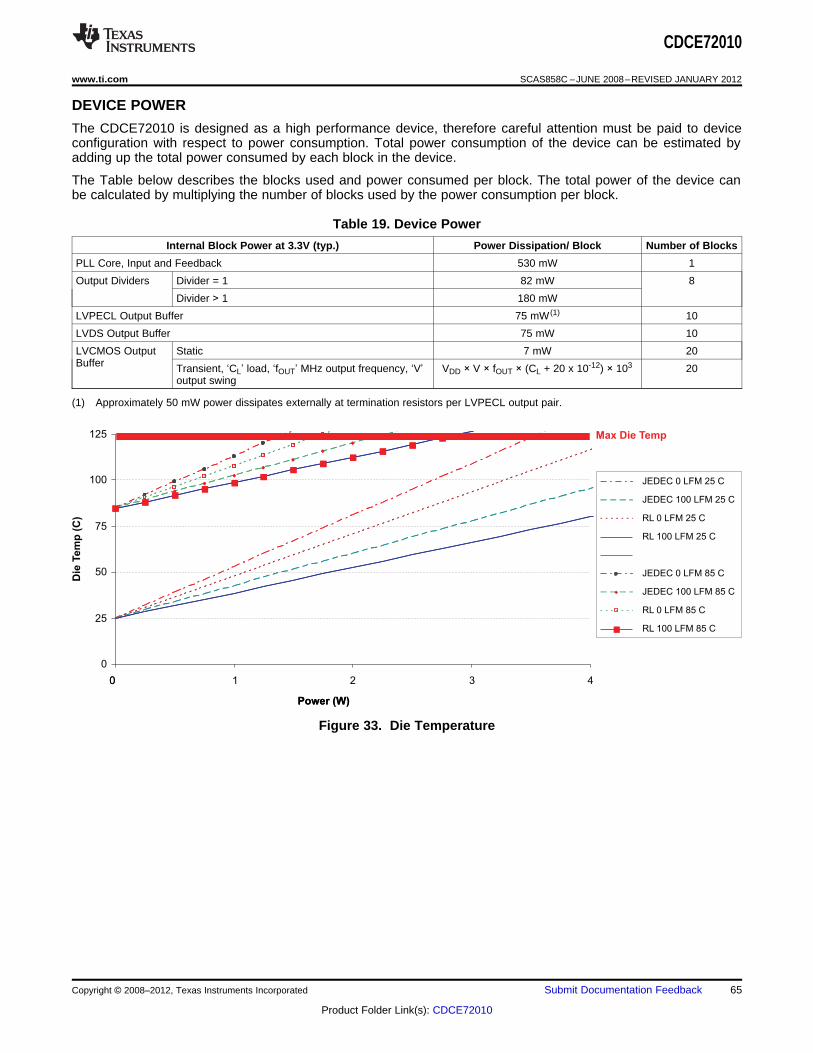
0
Power (W)
0
25
50
75
100
125
0 1 2 3 4
Power (W)
Die
Tem
p (
C)
JEDEC 0 LFM 25 C
JEDEC 100 LFM 25 C
RL 0 LFM 25 C
RL 100 LFM 25 C
JEDEC 0 LFM 85 C
JEDEC 100 LFM 85 C
RL 0 LFM 85 C
RL 100 LFM 85 C
Max Die Temp
CDCE72010
www.ti.com SCAS858C –JUNE 2008–REVISED JANUARY 2012
DEVICE POWER
The CDCE72010 is designed as a high performance device, therefore careful attention must be paid to deviceconfiguration with respect to power consumption. Total power consumption of the device can be estimated byadding up the total power consumed by each block in the device.
The Table below describes the blocks used and power consumed per block. The total power of the device canbe calculated by multiplying the number of blocks used by the power consumption per block.
Table 19. Device Power
Internal Block Power at 3.3V (typ.) Power Dissipation/ Block Number of Blocks
PLL Core, Input and Feedback 530 mW 1
Output Dividers Divider = 1 82 mW 8
Divider > 1 180 mW
LVPECL Output Buffer 75 mW (1) 10
LVDS Output Buffer 75 mW 10
LVCMOS Output Static 7 mW 20Buffer Transient, ‘CL’ load, ‘fOUT’ MHz output frequency, ‘V’ VDD × V × fOUT × (CL + 20 x 10-12) × 103 20
output swing
(1) Approximately 50 mW power dissipates externally at termination resistors per LVPECL output pair.
Figure 33. Die Temperature
Copyright © 2008–2012, Texas Instruments Incorporated Submit Documentation Feedback 65
Product Folder Link(s): CDCE72010
VccCP
CDCE72010
C1
C2
R2
R3
C3
ChargePump
VCO/VCXO
Clock Out
VccCP
CDCE72010
SCAS858C –JUNE 2008–REVISED JANUARY 2012 www.ti.com
LOOP FILTER
The CDCE72010 is designed to control an external Voltage Controlled Oscillator (VCO) or a Voltage ControlledCrystal Oscillator (VCXO) and to synchronize the controlled oscillators to the input reference. Controlling theOscillator happens via a DC voltage that is applied to the Voltage control pin. This DC voltage is generated bythe CDCE72010 in the form of AC pulses that get filtered by the external loop filter.
Figure 34. Loop Filter
66 Submit Documentation Feedback Copyright © 2008–2012, Texas Instruments Incorporated
Product Folder Link(s): CDCE72010
LVCMOS
LVCMOS
LVPECL
LVDS
Register (0 to 9)
RAM Bits:: 21 22 23 24 25 26 27
CDCE72010
www.ti.com SCAS858C –JUNE 2008–REVISED JANUARY 2012
UNIVERSAL OUTPUT BUFFERS
The CDCE72010 is designed to drive three types of clock signaling, LVPECL, LVDS, and LVCMOS from each ofthe ten outputs. This super buffer that contains all three drivers is refered to as the Universal Output Buffer. Onlyone driver can be enabled at one time. Each universal output buffer is made from four independent buffers inparallel. When LVPECL mode is selected, only the LVPECL Buffer is enabled and the rest of the buffers are3-stated and in low power mode. When Selecting LVDS, only the LVDS Buffer is enabled and the rest of thebuffers are 3-stated and in low power mode. When LVCMOS mode is selected, both LVCMOS drivers areenabled. One LVCMOS buffer drives the negative side and the other buffer drives the positive pin.
The LVCMOS drivers are driven from the same output divider but have separate control bits. In SPI Mode, bits22, 23, 24, and 25 of Registers 0 to 9 are used to put the LVCMOS buffer in active, inverting, low, or 3-state. InCD Mode, those bits are used for different functions and the LVCMOS buffer can be active when selected or3-state when their not.
Figure 35. Universal Output Buffer
Copyright © 2008–2012, Texas Instruments Incorporated Submit Documentation Feedback 67
Product Folder Link(s): CDCE72010
Reference Clock
REG0<Bit4> VCXOSEL
“1” “0” REG6<Bit5>
DET_START_BYPASSREG6<Bit2> FB_DETERM_DIV_SEL
“0” Feedback Divider Clock
“1” Divide by 2 Feedback Clock
Any of the Conditions will Produce a Conditional SYNC Start Signal:
1- REG9 <Bit11> INDET_BP is set to “0” & VCXO or AUX_CLK is available
2- REG9<Bit12> PLL_LOCK_BP is set to “0” & we have 1st Lock State
3- REG11<Bit19> PD_PLL is set to “0”& the PLL is ON
4- REG9<Bit13> LOW_FD_FB_EN is set to “1” N Divider Input Frequency above 600KHz
5- Write Activity to the Output Divider (s)
6- REG12<Bit8> Set to 1 ( /RESET Bit is Set to “1”)
7- REG12<Bit7> Set to 1 ( /Power Down Bit is Set to “1”)
/RESET Pin
“0” 1” REG9<Bit10>
STARTBYPASS
Feedback Clock
“0”
“1”
OUTPUT DIVIDERS SYNC SIGNAL
Synchronizing Output Divider SYNC Signal
If the value of the bits described as inverted the function associated with it will be ignored
with respect to the sync start signal generation.
CDCE72010
SCAS858C –JUNE 2008–REVISED JANUARY 2012 www.ti.com
Output Dividers Synchronization
The CDCE72010 is a 10 output clock device with 8 output dividers and to insure that all the outputs aresynchronous a synchronization startup circuitry is used. The synchronization circuitry generates a pulse to resetall the dividers in a way, that a predictable synchronous output is generated. The Synchronization signal can begenerated from different sources and can be synchronized to a specific clock. The Block diagram belowillustrates the signal path of the Output Divider Sync Signal. This function is assured up to 500 MHz.
NOTEThe minimum frequency required for the output synchronization block to work properly is 1MHz.
Figure 36. Output Divider Synchronization Block Diagram
68 Submit Documentation Feedback Copyright © 2008–2012, Texas Instruments Incorporated
Product Folder Link(s): CDCE72010
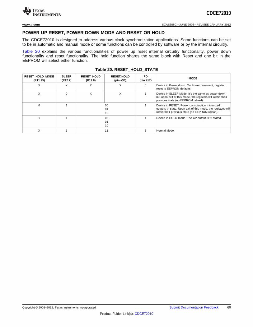
CDCE72010
www.ti.com SCAS858C –JUNE 2008–REVISED JANUARY 2012
POWER UP RESET, POWER DOWN MODE AND RESET OR HOLD
The CDCE72010 is designed to address various clock synchronization applications. Some functions can be setto be in automatic and manual mode or some functions can be controlled by software or by the internal circuitry.
Table 20 explains the various functionalities of power up reset internal circuitry functionality, power downfunctionality and reset functionality. The hold function shares the same block with Reset and one bit in theEEPROM will select either function.
Table 20. RESET_HOLD_STATE
RESET_HOLD_MODE SLEEP RESET_HOLD RESET/HOLD PDMODE
(R11.25) (R12.7) (R12.8) (pin #33) (pin #17)
X X X X 0 Device in Power down. On Power down exit, registerreset to EEPROM defaults.
X 0 X X 1 Device in SLEEP Mode. It’s the same as power downbut upon exit of this mode, the registers will retain theirprevious state (no EEPROM reload).
0 1 00 1 Device in RESET. Power consumption minimizedoutputs tri-state. Upon exit of this mode, the registers will01retain their previous state (no EEPROM reload).10
1 1 00 1 Device in HOLD mode. The CP output is tri-stated.0110
X 1 11 1 Normal Mode.
Copyright © 2008–2012, Texas Instruments Incorporated Submit Documentation Feedback 69
Product Folder Link(s): CDCE72010
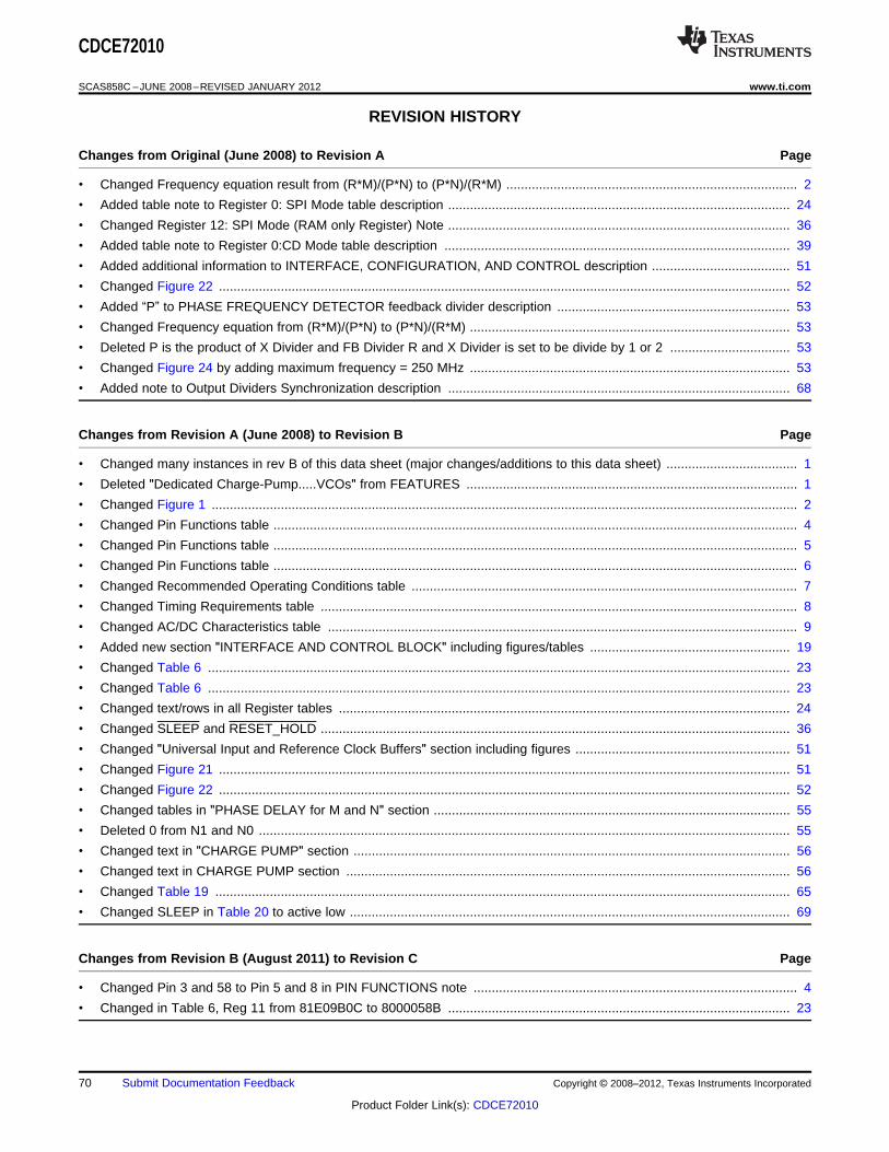
CDCE72010
SCAS858C –JUNE 2008–REVISED JANUARY 2012 www.ti.com
REVISION HISTORY
Changes from Original (June 2008) to Revision A Page
• Changed Frequency equation result from (R*M)/(P*N) to (P*N)/(R*M) ................................................................................ 2
• Added table note to Register 0: SPI Mode table description .............................................................................................. 24
• Changed Register 12: SPI Mode (RAM only Register) Note .............................................................................................. 36
• Added table note to Register 0:CD Mode table description ............................................................................................... 39
• Added additional information to INTERFACE, CONFIGURATION, AND CONTROL description ...................................... 51
• Changed Figure 22 ............................................................................................................................................................. 52
• Added “P” to PHASE FREQUENCY DETECTOR feedback divider description ................................................................ 53
• Changed Frequency equation from (R*M)/(P*N) to (P*N)/(R*M) ........................................................................................ 53
• Deleted P is the product of X Divider and FB Divider R and X Divider is set to be divide by 1 or 2 ................................. 53
• Changed Figure 24 by adding maximum frequency = 250 MHz ........................................................................................ 53
• Added note to Output Dividers Synchronization description .............................................................................................. 68
Changes from Revision A (June 2008) to Revision B Page
• Changed many instances in rev B of this data sheet (major changes/additions to this data sheet) .................................... 1
• Deleted "Dedicated Charge-Pump.....VCOs" from FEATURES ........................................................................................... 1
• Changed Figure 1 ................................................................................................................................................................. 2
• Changed Pin Functions table ................................................................................................................................................ 4
• Changed Pin Functions table ................................................................................................................................................ 5
• Changed Pin Functions table ................................................................................................................................................ 6
• Changed Recommended Operating Conditions table .......................................................................................................... 7
• Changed Timing Requirements table ................................................................................................................................... 8
• Changed AC/DC Characteristics table ................................................................................................................................. 9
• Added new section "INTERFACE AND CONTROL BLOCK" including figures/tables ....................................................... 19
• Changed Table 6 ................................................................................................................................................................ 23
• Changed Table 6 ................................................................................................................................................................ 23
• Changed text/rows in all Register tables ............................................................................................................................ 24
• Changed SLEEP and RESET_HOLD ................................................................................................................................. 36
• Changed "Universal Input and Reference Clock Buffers" section including figures ........................................................... 51
• Changed Figure 21 ............................................................................................................................................................. 51
• Changed Figure 22 ............................................................................................................................................................. 52
• Changed tables in "PHASE DELAY for M and N" section .................................................................................................. 55
• Deleted 0 from N1 and N0 .................................................................................................................................................. 55
• Changed text in "CHARGE PUMP" section ........................................................................................................................ 56
• Changed text in CHARGE PUMP section .......................................................................................................................... 56
• Changed Table 19 .............................................................................................................................................................. 65
• Changed SLEEP in Table 20 to active low ......................................................................................................................... 69
Changes from Revision B (August 2011) to Revision C Page
• Changed Pin 3 and 58 to Pin 5 and 8 in PIN FUNCTIONS note ......................................................................................... 4
• Changed in Table 6, Reg 11 from 81E09B0C to 8000058B .............................................................................................. 23
70 Submit Documentation Feedback Copyright © 2008–2012, Texas Instruments Incorporated
Product Folder Link(s): CDCE72010
PACKAGE OPTION ADDENDUM
www.ti.com 11-Apr-2013
Addendum-Page 1
PACKAGING INFORMATION
Orderable Device Status(1)
Package Type PackageDrawing
Pins PackageQty
Eco Plan(2)
Lead/Ball Finish MSL Peak Temp(3)
Op Temp (°C) Top-Side Markings(4)
Samples
CDCE72010RGCR ACTIVE VQFN RGC 64 2000 Green (RoHS& no Sb/Br)
CU NIPDAU Level-3-260C-168 HR -40 to 85 CDCE72010
CDCE72010RGCRG4 ACTIVE VQFN RGC 64 2000 Green (RoHS& no Sb/Br)
CU NIPDAU Level-3-260C-168 HR -40 to 85 CDCE72010
CDCE72010RGCT ACTIVE VQFN RGC 64 250 Green (RoHS& no Sb/Br)
CU NIPDAU Level-3-260C-168 HR -40 to 85 CDCE72010
CDCE72010RGCTG4 ACTIVE VQFN RGC 64 250 Green (RoHS& no Sb/Br)
CU NIPDAU Level-3-260C-168 HR -40 to 85 CDCE72010
(1) The marketing status values are defined as follows:ACTIVE: Product device recommended for new designs.LIFEBUY: TI has announced that the device will be discontinued, and a lifetime-buy period is in effect.NRND: Not recommended for new designs. Device is in production to support existing customers, but TI does not recommend using this part in a new design.PREVIEW: Device has been announced but is not in production. Samples may or may not be available.OBSOLETE: TI has discontinued the production of the device.
(2) Eco Plan - The planned eco-friendly classification: Pb-Free (RoHS), Pb-Free (RoHS Exempt), or Green (RoHS & no Sb/Br) - please check http://www.ti.com/productcontent for the latest availabilityinformation and additional product content details.TBD: The Pb-Free/Green conversion plan has not been defined.Pb-Free (RoHS): TI's terms "Lead-Free" or "Pb-Free" mean semiconductor products that are compatible with the current RoHS requirements for all 6 substances, including the requirement thatlead not exceed 0.1% by weight in homogeneous materials. Where designed to be soldered at high temperatures, TI Pb-Free products are suitable for use in specified lead-free processes.Pb-Free (RoHS Exempt): This component has a RoHS exemption for either 1) lead-based flip-chip solder bumps used between the die and package, or 2) lead-based die adhesive used betweenthe die and leadframe. The component is otherwise considered Pb-Free (RoHS compatible) as defined above.Green (RoHS & no Sb/Br): TI defines "Green" to mean Pb-Free (RoHS compatible), and free of Bromine (Br) and Antimony (Sb) based flame retardants (Br or Sb do not exceed 0.1% by weightin homogeneous material)
(3) MSL, Peak Temp. -- The Moisture Sensitivity Level rating according to the JEDEC industry standard classifications, and peak solder temperature.
(4) Multiple Top-Side Markings will be inside parentheses. Only one Top-Side Marking contained in parentheses and separated by a "~" will appear on a device. If a line is indented then it is acontinuation of the previous line and the two combined represent the entire Top-Side Marking for that device.
Important Information and Disclaimer:The information provided on this page represents TI's knowledge and belief as of the date that it is provided. TI bases its knowledge and belief on informationprovided by third parties, and makes no representation or warranty as to the accuracy of such information. Efforts are underway to better integrate information from third parties. TI has taken andcontinues to take reasonable steps to provide representative and accurate information but may not have conducted destructive testing or chemical analysis on incoming materials and chemicals.TI and TI suppliers consider certain information to be proprietary, and thus CAS numbers and other limited information may not be available for release.
In no event shall TI's liability arising out of such information exceed the total purchase price of the TI part(s) at issue in this document sold by TI to Customer on an annual basis.
PACKAGE OPTION ADDENDUM
www.ti.com 11-Apr-2013
Addendum-Page 2
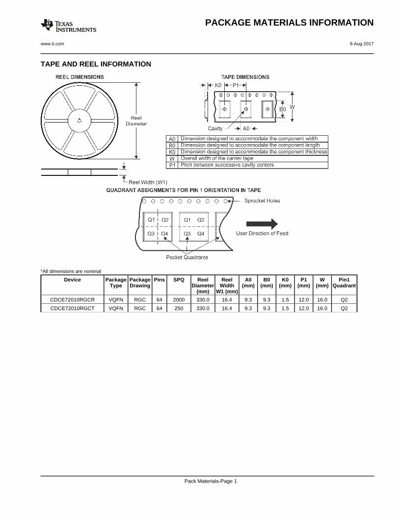
TAPE AND REEL INFORMATION
*All dimensions are nominal
Device PackageType
PackageDrawing
Pins SPQ ReelDiameter
(mm)
ReelWidth
W1 (mm)
A0(mm)
B0(mm)
K0(mm)
P1(mm)
W(mm)
Pin1Quadrant
CDCE72010RGCR VQFN RGC 64 2000 330.0 16.4 9.3 9.3 1.5 12.0 16.0 Q2
CDCE72010RGCT VQFN RGC 64 250 330.0 16.4 9.3 9.3 1.5 12.0 16.0 Q2
PACKAGE MATERIALS INFORMATION
www.ti.com 9-Aug-2017
Pack Materials-Page 1
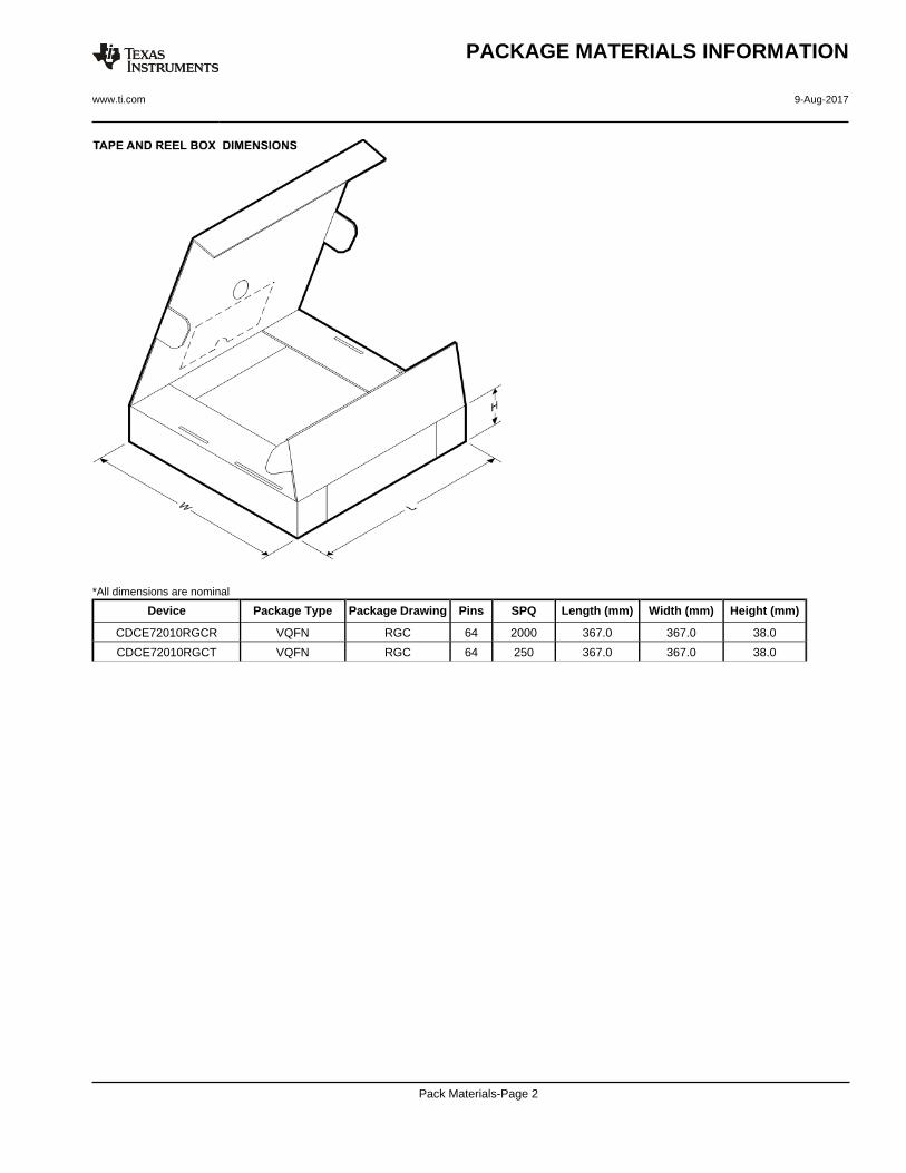
*All dimensions are nominal
Device Package Type Package Drawing Pins SPQ Length (mm) Width (mm) Height (mm)
CDCE72010RGCR VQFN RGC 64 2000 367.0 367.0 38.0
CDCE72010RGCT VQFN RGC 64 250 367.0 367.0 38.0
PACKAGE MATERIALS INFORMATION
www.ti.com 9-Aug-2017
Pack Materials-Page 2
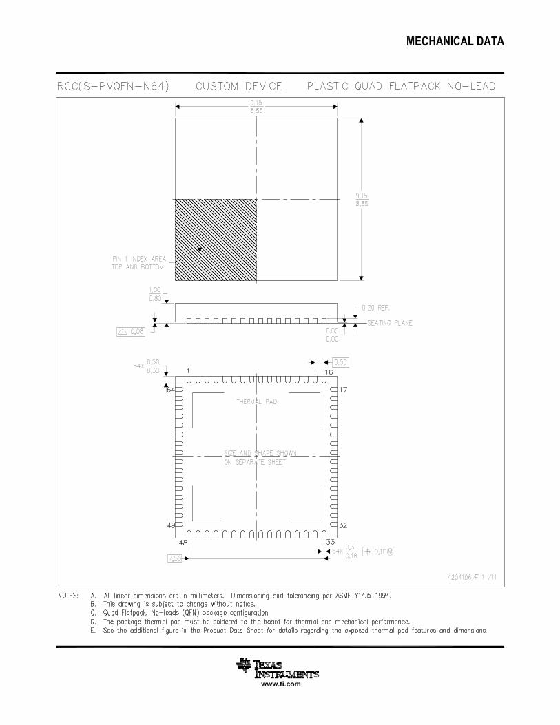

IMPORTANT NOTICE
Texas Instruments Incorporated (TI) reserves the right to make corrections, enhancements, improvements and other changes to itssemiconductor products and services per JESD46, latest issue, and to discontinue any product or service per JESD48, latest issue. Buyersshould obtain the latest relevant information before placing orders and should verify that such information is current and complete.TI’s published terms of sale for semiconductor products (http://www.ti.com/sc/docs/stdterms.htm) apply to the sale of packaged integratedcircuit products that TI has qualified and released to market. Additional terms may apply to the use or sale of other types of TI products andservices.Reproduction of significant portions of TI information in TI data sheets is permissible only if reproduction is without alteration and isaccompanied by all associated warranties, conditions, limitations, and notices. TI is not responsible or liable for such reproduceddocumentation. Information of third parties may be subject to additional restrictions. Resale of TI products or services with statementsdifferent from or beyond the parameters stated by TI for that product or service voids all express and any implied warranties for theassociated TI product or service and is an unfair and deceptive business practice. TI is not responsible or liable for any such statements.Buyers and others who are developing systems that incorporate TI products (collectively, “Designers”) understand and agree that Designersremain responsible for using their independent analysis, evaluation and judgment in designing their applications and that Designers havefull and exclusive responsibility to assure the safety of Designers' applications and compliance of their applications (and of all TI productsused in or for Designers’ applications) with all applicable regulations, laws and other applicable requirements. Designer represents that, withrespect to their applications, Designer has all the necessary expertise to create and implement safeguards that (1) anticipate dangerousconsequences of failures, (2) monitor failures and their consequences, and (3) lessen the likelihood of failures that might cause harm andtake appropriate actions. Designer agrees that prior to using or distributing any applications that include TI products, Designer willthoroughly test such applications and the functionality of such TI products as used in such applications.TI’s provision of technical, application or other design advice, quality characterization, reliability data or other services or information,including, but not limited to, reference designs and materials relating to evaluation modules, (collectively, “TI Resources”) are intended toassist designers who are developing applications that incorporate TI products; by downloading, accessing or using TI Resources in anyway, Designer (individually or, if Designer is acting on behalf of a company, Designer’s company) agrees to use any particular TI Resourcesolely for this purpose and subject to the terms of this Notice.TI’s provision of TI Resources does not expand or otherwise alter TI’s applicable published warranties or warranty disclaimers for TIproducts, and no additional obligations or liabilities arise from TI providing such TI Resources. TI reserves the right to make corrections,enhancements, improvements and other changes to its TI Resources. TI has not conducted any testing other than that specificallydescribed in the published documentation for a particular TI Resource.Designer is authorized to use, copy and modify any individual TI Resource only in connection with the development of applications thatinclude the TI product(s) identified in such TI Resource. NO OTHER LICENSE, EXPRESS OR IMPLIED, BY ESTOPPEL OR OTHERWISETO ANY OTHER TI INTELLECTUAL PROPERTY RIGHT, AND NO LICENSE TO ANY TECHNOLOGY OR INTELLECTUAL PROPERTYRIGHT OF TI OR ANY THIRD PARTY IS GRANTED HEREIN, including but not limited to any patent right, copyright, mask work right, orother intellectual property right relating to any combination, machine, or process in which TI products or services are used. Informationregarding or referencing third-party products or services does not constitute a license to use such products or services, or a warranty orendorsement thereof. Use of TI Resources may require a license from a third party under the patents or other intellectual property of thethird party, or a license from TI under the patents or other intellectual property of TI.TI RESOURCES ARE PROVIDED “AS IS” AND WITH ALL FAULTS. TI DISCLAIMS ALL OTHER WARRANTIES ORREPRESENTATIONS, EXPRESS OR IMPLIED, REGARDING RESOURCES OR USE THEREOF, INCLUDING BUT NOT LIMITED TOACCURACY OR COMPLETENESS, TITLE, ANY EPIDEMIC FAILURE WARRANTY AND ANY IMPLIED WARRANTIES OFMERCHANTABILITY, FITNESS FOR A PARTICULAR PURPOSE, AND NON-INFRINGEMENT OF ANY THIRD PARTY INTELLECTUALPROPERTY RIGHTS. TI SHALL NOT BE LIABLE FOR AND SHALL NOT DEFEND OR INDEMNIFY DESIGNER AGAINST ANY CLAIM,INCLUDING BUT NOT LIMITED TO ANY INFRINGEMENT CLAIM THAT RELATES TO OR IS BASED ON ANY COMBINATION OFPRODUCTS EVEN IF DESCRIBED IN TI RESOURCES OR OTHERWISE. IN NO EVENT SHALL TI BE LIABLE FOR ANY ACTUAL,DIRECT, SPECIAL, COLLATERAL, INDIRECT, PUNITIVE, INCIDENTAL, CONSEQUENTIAL OR EXEMPLARY DAMAGES INCONNECTION WITH OR ARISING OUT OF TI RESOURCES OR USE THEREOF, AND REGARDLESS OF WHETHER TI HAS BEENADVISED OF THE POSSIBILITY OF SUCH DAMAGES.Unless TI has explicitly designated an individual product as meeting the requirements of a particular industry standard (e.g., ISO/TS 16949and ISO 26262), TI is not responsible for any failure to meet such industry standard requirements.Where TI specifically promotes products as facilitating functional safety or as compliant with industry functional safety standards, suchproducts are intended to help enable customers to design and create their own applications that meet applicable functional safety standardsand requirements. Using products in an application does not by itself establish any safety features in the application. Designers mustensure compliance with safety-related requirements and standards applicable to their applications. Designer may not use any TI products inlife-critical medical equipment unless authorized officers of the parties have executed a special contract specifically governing such use.Life-critical medical equipment is medical equipment where failure of such equipment would cause serious bodily injury or death (e.g., lifesupport, pacemakers, defibrillators, heart pumps, neurostimulators, and implantables). Such equipment includes, without limitation, allmedical devices identified by the U.S. Food and Drug Administration as Class III devices and equivalent classifications outside the U.S.TI may expressly designate certain products as completing a particular qualification (e.g., Q100, Military Grade, or Enhanced Product).Designers agree that it has the necessary expertise to select the product with the appropriate qualification designation for their applicationsand that proper product selection is at Designers’ own risk. Designers are solely responsible for compliance with all legal and regulatoryrequirements in connection with such selection.Designer will fully indemnify TI and its representatives against any damages, costs, losses, and/or liabilities arising out of Designer’s non-compliance with the terms and provisions of this Notice.
Mailing Address: Texas Instruments, Post Office Box 655303, Dallas, Texas 75265Copyright © 2017, Texas Instruments Incorporated