Propositional-Logic Typing - Developing a Logic System for ...
This is information on a product in full production.
January 2013 Doc ID 14321 Rev 5 1/32
32
L6228Q
DMOS driver for bipolar stepper motor
Datasheet − production data
Features■ Operating supply voltage from 8 to 52 V
■ 2.8 A output peak current (1.4 Ar.m.s.)
■ RDS(on) 0.73 Ω typ. value @ TJ = 25 °C
■ Operating frequency up to 100 kHz
■ Non dissipative overcurrent protection
■ Dual independent constant tOFF PWM current controllers
■ Fast/slow decay mode selection
■ Fast decay quasi-synchronous rectification
■ Decoding logic for stepper motor full and half- step drive
■ Cross conduction protection
■ Thermal shutdown
■ Undervoltage lockout
■ Integrated fast free wheeling diodes
Applications■ Bipolar stepper motor
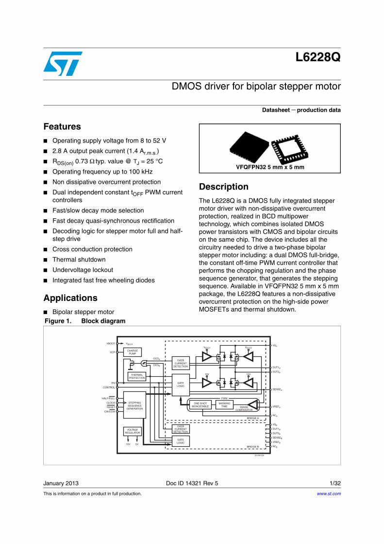
DescriptionThe L6228Q is a DMOS fully integrated stepper motor driver with non-dissipative overcurrent protection, realized in BCD multipower technology, which combines isolated DMOS power transistors with CMOS and bipolar circuits on the same chip. The device includes all the circuitry needed to drive a two-phase bipolar stepper motor including: a dual DMOS full-bridge, the constant off-time PWM current controller that performs the chopping regulation and the phase sequence generator, that generates the stepping sequence. Available in VFQFPN32 5 mm x 5 mm package, the L6228Q features a non-dissipative overcurrent protection on the high-side power MOSFETs and thermal shutdown.
VFQFPN32 5 mm x 5 mm
Figure 1. Block diagram
GATELOGIC
STEPPINGSEQUENCE
GENERATION
OVERCURRENT
DETECTION
OVERCURRENT
DETECTION
GATELOGIC
VCP
VBOOT
EN
CONTROL
CW/CCW
VREFA
VBOOT
5V10V
VSA
VSB
OUT1A
OUT2A
OUT1B
OUT2B
SENSEA
CHARGEPUMP
VOLTAGEREGULATOR
ONE SHOTMONOSTABLE
MASKINGTIME
THERMALPROTECTION
VBOOT VBOOT
OCDB
OCDA
10V 10V
BRIDGE A
SENSECOMPARATOR
BRIDGE B
D01IN1225
RCA
+
-
SENSEB
VREFB
RCB
HALF/FULL
CLOCK
RESET
PWM
www.st.com
Contents L6228Q
2/32 Doc ID 14321 Rev 5
Contents
1 Electrical data . . . . . . . . . . . . . . . . . . . . . . . . . . . . . . . . . . . . . . . . . . . . . . 3
1.1 Absolute maximum ratings . . . . . . . . . . . . . . . . . . . . . . . . . . . . . . . . . . . . . 3
1.2 Recommended operating conditions . . . . . . . . . . . . . . . . . . . . . . . . . . . . . 3
1.3 Thermal data . . . . . . . . . . . . . . . . . . . . . . . . . . . . . . . . . . . . . . . . . . . . . . . 4
2 Pin connection . . . . . . . . . . . . . . . . . . . . . . . . . . . . . . . . . . . . . . . . . . . . . . 5
3 Electrical characteristics . . . . . . . . . . . . . . . . . . . . . . . . . . . . . . . . . . . . . 7
4 Circuit description . . . . . . . . . . . . . . . . . . . . . . . . . . . . . . . . . . . . . . . . . . 11
4.1 Power stages and charge pump . . . . . . . . . . . . . . . . . . . . . . . . . . . . . . . . 11
4.2 Logic inputs . . . . . . . . . . . . . . . . . . . . . . . . . . . . . . . . . . . . . . . . . . . . . . . 12
4.3 PWM current control . . . . . . . . . . . . . . . . . . . . . . . . . . . . . . . . . . . . . . . . . 13
4.4 Decay modes . . . . . . . . . . . . . . . . . . . . . . . . . . . . . . . . . . . . . . . . . . . . . . 16
4.5 Stepping sequence generation . . . . . . . . . . . . . . . . . . . . . . . . . . . . . . . . . 17
4.6 Half-step mode . . . . . . . . . . . . . . . . . . . . . . . . . . . . . . . . . . . . . . . . . . . . . 17
4.7 Normal drive mode (full-step two-phase-on) . . . . . . . . . . . . . . . . . . . . . . 18
4.8 Wave drive mode (full-step one-phase-on) . . . . . . . . . . . . . . . . . . . . . . . 18
4.9 Non-dissipative overcurrent protection . . . . . . . . . . . . . . . . . . . . . . . . . . . 19
4.10 Thermal protection . . . . . . . . . . . . . . . . . . . . . . . . . . . . . . . . . . . . . . . . . . 22
5 Application information . . . . . . . . . . . . . . . . . . . . . . . . . . . . . . . . . . . . . 23
6 Output current capability and IC power dissipation . . . . . . . . . . . . . . 25
7 Thermal management . . . . . . . . . . . . . . . . . . . . . . . . . . . . . . . . . . . . . . . 27
8 Package mechanical data . . . . . . . . . . . . . . . . . . . . . . . . . . . . . . . . . . . . 28
9 Ordering information . . . . . . . . . . . . . . . . . . . . . . . . . . . . . . . . . . . . . . . 30
10 Revision history . . . . . . . . . . . . . . . . . . . . . . . . . . . . . . . . . . . . . . . . . . . 31
L6228Q Electrical data
Doc ID 14321 Rev 5 3/32
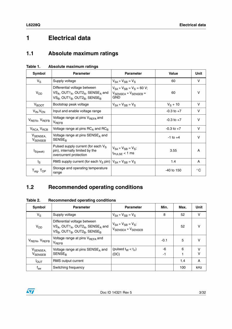
1 Electrical data
1.1 Absolute maximum ratings
1.2 Recommended operating conditions
Table 1. Absolute maximum ratings
Symbol Parameter Parameter Value Unit
VS Supply voltage VSA = VSB = VS 60 V
VOD
Differential voltage betweenVSA, OUT1A, OUT2A, SENSEA and VSB, OUT1B, OUT2B, SENSEB
VSA = VSB = VS = 60 V;VSENSEA = VSENSEB = GND
60 V
VBOOT Bootstrap peak voltage VSA = VSB = VS VS + 10 V
VIN,VEN Input and enable voltage range -0.3 to +7 V
VREFA, VREFBVoltage range at pins VREFA and VREFB
-0.3 to +7 V
VRCA, VRCB Voltage range at pins RCA and RCB -0.3 to +7 V
VSENSEA, VSENSEB
Voltage range at pins SENSEA and SENSEB
-1 to +4 V
IS(peak)
Pulsed supply current (for each VS pin), internally limited by the overcurrent protection
VSA = VSB = VS;
tPULSE < 1 ms3.55 A
IS RMS supply current (for each VS pin) VSA = VSB = VS 1.4 A
Tstg, TOPStorage and operating temperature range
-40 to 150 ° C
Table 2. Recommended operating conditions
Symbol Parameter Parameter Min. Max. Unit
VS Supply voltage VSA = VSB = VS 8 52 V
VOD
Differential voltage betweenVSA, OUT1A, OUT2A, SENSEA and VSB, OUT1B, OUT2B, SENSEB
VSA = VSB = VS;VSENSEA = VSENSEB
52 V
VREFA, VREFBVoltage range at pins VREFA and VREFB
-0.1 5 V
VSENSEA, VSENSEB
Voltage range at pins SENSEA and SENSEB
(pulsed tW < trr)
(DC)
-6
-1
6
1VV
IOUT RMS output current 1.4 A
fsw Switching frequency 100 kHz
Electrical data L6228Q
4/32 Doc ID 14321 Rev 5
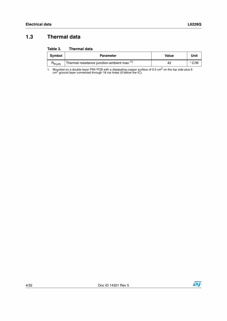
1.3 Thermal data
Table 3. Thermal data
Symbol Parameter Value Unit
Rth(JA) Thermal resistance junction-ambient max (1)
1. Mounted on a double-layer FR4 PCB with a dissipating copper surface of 0.5 cm2 on the top side plus 6 cm2 ground layer connected through 18 via holes (9 below the IC).
42 ° C/W
L6228Q Pin connection
Doc ID 14321 Rev 5 5/32
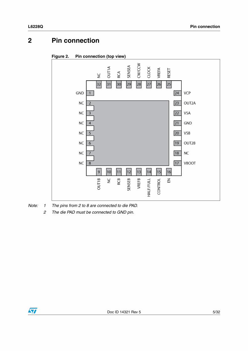
2 Pin connection
Figure 2. Pin connection (top view)
Note: 1 The pins from 2 to 8 are connected to die PAD.
2 The die PAD must be connected to GND pin.
Pin connection L6228Q
6/32 Doc ID 14321 Rev 5
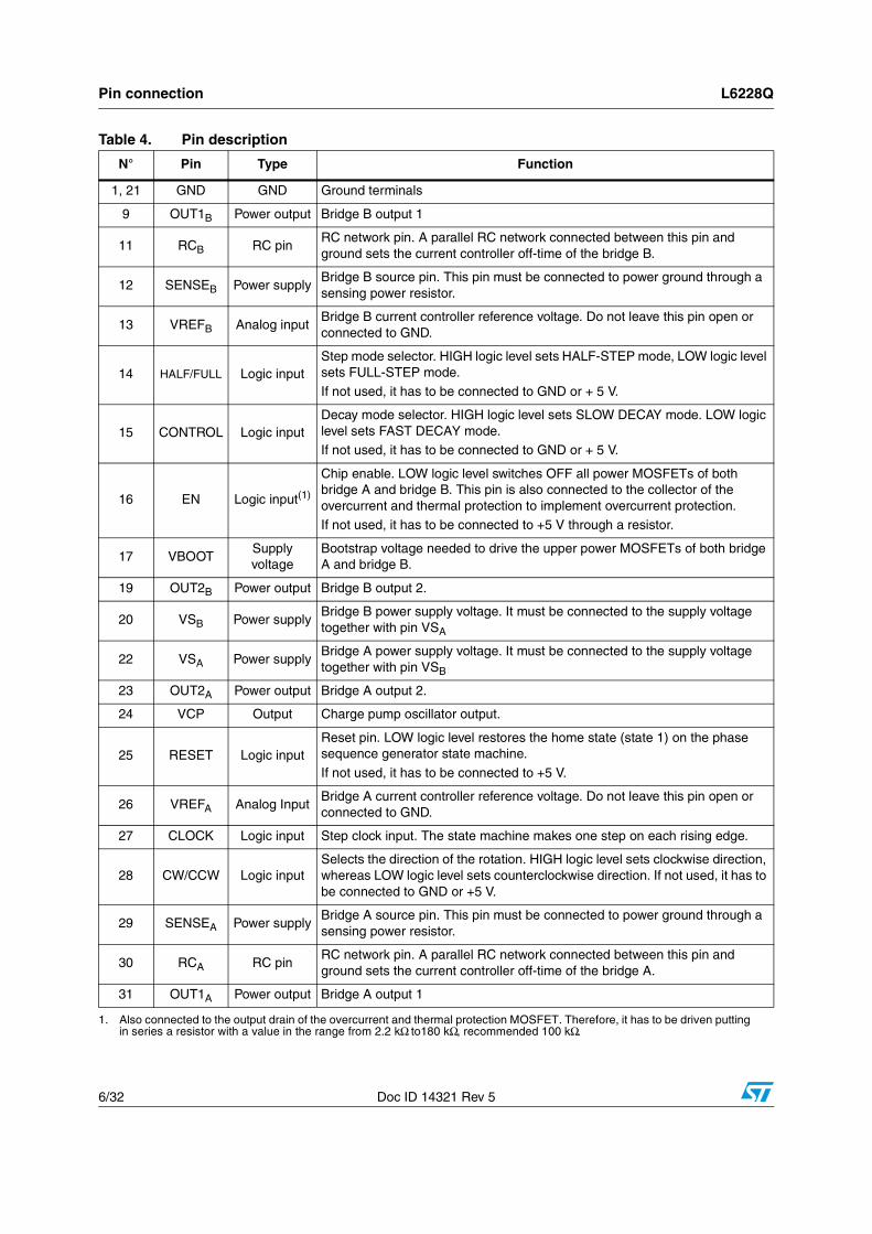
Table 4. Pin description
N° Pin Type Function
1, 21 GND GND Ground terminals
9 OUT1B Power output Bridge B output 1
11 RCB RC pinRC network pin. A parallel RC network connected between this pin and ground sets the current controller off-time of the bridge B.
12 SENSEB Power supplyBridge B source pin. This pin must be connected to power ground through a sensing power resistor.
13 VREFB Analog inputBridge B current controller reference voltage. Do not leave this pin open or connected to GND.
14 HALF/FULL Logic inputStep mode selector. HIGH logic level sets HALF-STEP mode, LOW logic level sets FULL-STEP mode. If not used, it has to be connected to GND or + 5 V.
15 CONTROL Logic inputDecay mode selector. HIGH logic level sets SLOW DECAY mode. LOW logic level sets FAST DECAY mode. If not used, it has to be connected to GND or + 5 V.
16 EN Logic input(1)
Chip enable. LOW logic level switches OFF all power MOSFETs of both bridge A and bridge B. This pin is also connected to the collector of the overcurrent and thermal protection to implement overcurrent protection. If not used, it has to be connected to +5 V through a resistor.
17 VBOOTSupply voltage
Bootstrap voltage needed to drive the upper power MOSFETs of both bridge A and bridge B.
19 OUT2B Power output Bridge B output 2.
20 VSB Power supplyBridge B power supply voltage. It must be connected to the supply voltage together with pin VSA
22 VSA Power supplyBridge A power supply voltage. It must be connected to the supply voltage together with pin VSB
23 OUT2A Power output Bridge A output 2.
24 VCP Output Charge pump oscillator output.
25 RESET Logic inputReset pin. LOW logic level restores the home state (state 1) on the phase sequence generator state machine.
If not used, it has to be connected to +5 V.
26 VREFA Analog InputBridge A current controller reference voltage. Do not leave this pin open or connected to GND.
27 CLOCK Logic input Step clock input. The state machine makes one step on each rising edge.
28 CW/CCW Logic inputSelects the direction of the rotation. HIGH logic level sets clockwise direction, whereas LOW logic level sets counterclockwise direction. If not used, it has to be connected to GND or +5 V.
29 SENSEA Power supplyBridge A source pin. This pin must be connected to power ground through a sensing power resistor.
30 RCA RC pinRC network pin. A parallel RC network connected between this pin and ground sets the current controller off-time of the bridge A.
31 OUT1A Power output Bridge A output 1
1. Also connected to the output drain of the overcurrent and thermal protection MOSFET. Therefore, it has to be driven putting in series a resistor with a value in the range from 2.2 kΩ to180 kΩ, recommended 100 kΩ.
L6228Q Electrical characteristics
Doc ID 14321 Rev 5 7/32
3 Electrical characteristics
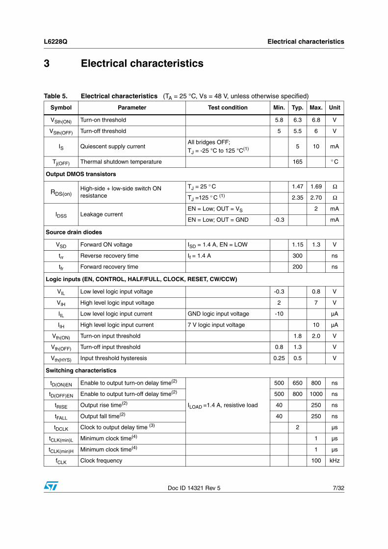
Table 5. Electrical characteristics (TA = 25 °C, Vs = 48 V, unless otherwise specified)
Symbol Parameter Test condition Min. Typ. Max. Unit
VSth(ON) Turn-on threshold 5.8 6.3 6.8 V
VSth(OFF) Turn-off threshold 5 5.5 6 V
IS Quiescent supply currentAll bridges OFF;TJ = -25 °C to 125 °C(1) 5 10 mA
Tj(OFF) Thermal shutdown temperature 165 ° C
Output DMOS transistors
RDS(on)High-side + low-side switch ON resistance
TJ = 25 ° C 1.47 1.69 Ω
TJ =125 ° C (1) 2.35 2.70 Ω
IDSS Leakage currentEN = Low; OUT = VS 2 mA
EN = Low; OUT = GND -0.3 mA
Source drain diodes
VSD Forward ON voltage ISD = 1.4 A, EN = LOW 1.15 1.3 V
trr Reverse recovery time If = 1.4 A 300 ns
tfr Forward recovery time 200 ns
Logic inputs (EN, CONTROL, HALF/FULL, CLOCK, RESET, CW/CCW)
VIL Low level logic input voltage -0.3 0.8 V
VIH High level logic input voltage 2 7 V
IIL Low level logic input current GND logic input voltage -10 µA
IIH High level logic input current 7 V logic input voltage 10 µA
Vth(ON) Turn-on input threshold 1.8 2.0 V
Vth(OFF) Turn-off input threshold 0.8 1.3 V
Vth(HYS) Input threshold hysteresis 0.25 0.5 V
Switching characteristics
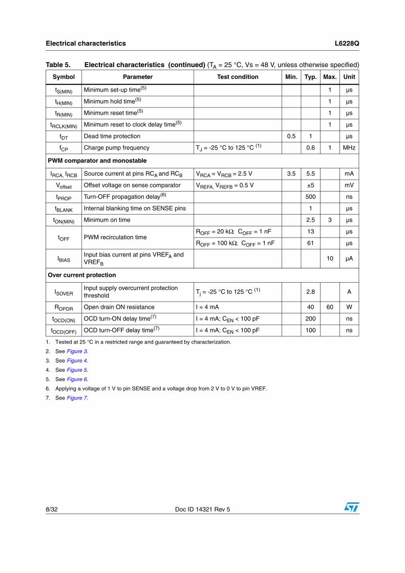
tD(ON)EN Enable to output turn-on delay time(2)
ILOAD =1.4 A, resistive load
500 650 800 ns
tD(OFF)EN Enable to output turn-off delay time(2) 500 800 1000 ns
tRISE Output rise time(2) 40 250 ns
tFALL Output fall time(2) 40 250 ns
tDCLK Clock to output delay time (3) 2 µs
tCLK(min)L Minimum clock time(4) 1 µs
tCLK(min)H Minimum clock time(4) 1 µs
fCLK Clock frequency 100 kHz
Electrical characteristics L6228Q
8/32 Doc ID 14321 Rev 5
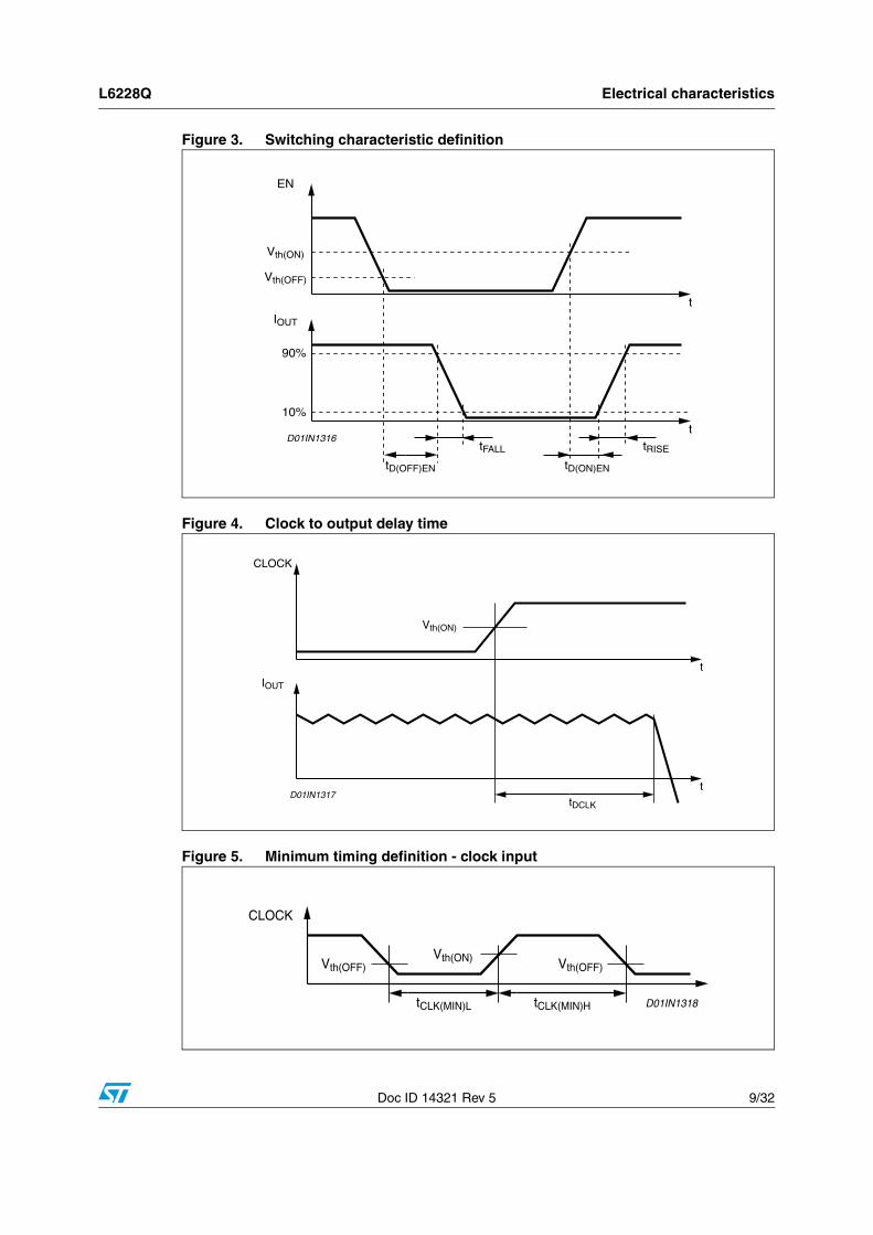
tS(MIN) Minimum set-up time(5) 1 µs
tH(MIN) Minimum hold time(5) 1 µs
tR(MIN) Minimum reset time(5) 1 µs
tRCLK(MIN) Minimum reset to clock delay time(5) 1 µs
tDT Dead time protection 0.5 1 µs
fCP Charge pump frequency TJ = -25 °C to 125 °C (1) 0.6 1 MHz
PWM comparator and monostable
IRCA, IRCB Source current at pins RCA and RCB VRCA = VRCB = 2.5 V 3.5 5.5 mA
Voffset Offset voltage on sense comparator VREFA, VREFB = 0.5 V ±5 mV
tPROP Turn-OFF propagation delay(6) 500 ns
tBLANK Internal blanking time on SENSE pins 1 µs
tON(MIN) Minimum on time 2.5 3 µs
tOFF PWM recirculation timeROFF = 20 kΩ; COFF = 1 nF 13 µs
ROFF = 100 kΩ; COFF = 1 nF 61 µs
IBIASInput bias current at pins VREFA and VREFB
10 µA
Over current protection
ISOVERInput supply overcurrent protection threshold
Tj = -25 °C to 125 °C (1) 2.8 A
ROPDR Open drain ON resistance I = 4 mA 40 60 W
tOCD(ON) OCD turn-ON delay time(7) I = 4 mA; CEN < 100 pF 200 ns
tOCD(OFF) OCD turn-OFF delay time(7) I = 4 mA; CEN < 100 pF 100 ns
1. Tested at 25 °C in a restricted range and guaranteed by characterization.
2. See Figure 3.
3. See Figure 4.
4. See Figure 5.
5. See Figure 6.
6. Applying a voltage of 1 V to pin SENSE and a voltage drop from 2 V to 0 V to pin VREF.
7. See Figure 7.
Table 5. Electrical characteristics (continued) (TA = 25 °C, Vs = 48 V, unless otherwise specified)
Symbol Parameter Test condition Min. Typ. Max. Unit
L6228Q Electrical characteristics
Doc ID 14321 Rev 5 9/32
Figure 3. Switching characteristic definition
Figure 4. Clock to output delay time
Figure 5. Minimum timing definition - clock input
Vth(ON)
Vth(OFF)
90%
10%
EN
IOUT
t
ttFALL
tD(OFF)EN
tRISE
tD(ON)EN
D01IN1316
CLOCK
IOUT
t
ttDCLK
Vth(ON)
D01IN1317
CLOCK
tCLK(MIN)HtCLK(MIN)L
Vth(OFF)Vth(ON)
D01IN1318
Vth(OFF)
Electrical characteristics L6228Q
10/32 Doc ID 14321 Rev 5
Figure 6. Minimum timing definition - logic inputs
Figure 7. Overcurrent detection timing definition
CLOCK
RESET
tS(MIN) tH(MIN)
tR(MIN) tRCLK(MIN)
LOGIC INPUTS
D01IN1319
Vth(OFF)Vth(ON)
Vth(ON)
ISOVER
90%
10%
IOUT
VEN
tOCD(OFF)tOCD(ON)D02IN1399
ON
OFF
BRIDGE
L6228Q Circuit description
Doc ID 14321 Rev 5 11/32
4 Circuit description
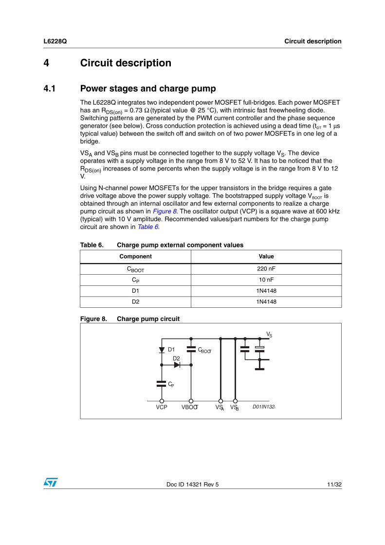
4.1 Power stages and charge pumpThe L6228Q integrates two independent power MOSFET full-bridges. Each power MOSFET has an RDS(on) = 0.73 Ω (typical value @ 25 °C), with intrinsic fast freewheeling diode. Switching patterns are generated by the PWM current controller and the phase sequence generator (see below). Cross conduction protection is achieved using a dead time (tDT = 1 μs typical value) between the switch off and switch on of two power MOSFETs in one leg of a bridge.
VSA and VSB pins must be connected together to the supply voltage VS. The device operates with a supply voltage in the range from 8 V to 52 V. It has to be noticed that the RDS(on) increases of some percents when the supply voltage is in the range from 8 V to 12 V.
Using N-channel power MOSFETs for the upper transistors in the bridge requires a gate drive voltage above the power supply voltage. The bootstrapped supply voltage VBOOT is obtained through an internal oscillator and few external components to realize a charge pump circuit as shown in Figure 8. The oscillator output (VCP) is a square wave at 600 kHz (typical) with 10 V amplitude. Recommended values/part numbers for the charge pump circuit are shown in Table 6.
Figure 8. Charge pump circuit
Table 6. Charge pump external component values
Component Value
CBOOT 220 nF
CP 10 nF
D1 1N4148
D2 1N4148
D2
CBOOTD1
CP
VS
VSAVCP VBOOT VSB D01IN1328
Circuit description L6228Q
12/32 Doc ID 14321 Rev 5
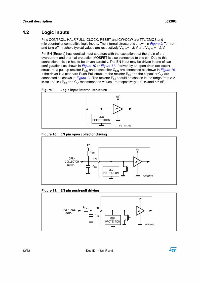
4.2 Logic inputsPins CONTROL, HALF/FULL, CLOCK, RESET and CW/CCW are TTL/CMOS and microcontroller compatible logic inputs. The internal structure is shown in Figure 9. Turn-on and turn-off threshold typical values are respectively Vth(ON)= 1.8 V and Vth(OFF)= 1.3 V.
Pin EN (Enable) has identical input structure with the exception that the drain of the overcurrent and thermal protection MOSFET is also connected to this pin. Due to this connection, this pin has to be driven carefully. The EN input may be driven in one of two configurations as shown in Figure 10 or Figure 11. If driven by an open drain (collector) structure, a pull-up resistor REN and a capacitor CEN are connected as shown in Figure 10. If the driver is a standard Push-Pull structure the resistor REN and the capacitor CEN are connected as shown in Figure 11. The resistor REN should be chosen in the range from 2.2 kΩ to 180 kΩ. REN and CEN recommended values are respectively 100 kΩ and 5.6 nF.
Figure 9. Logic input internal structure
Figure 10. EN pin open collector driving
Figure 11. EN pin push-pull driving
5V
D01IN1329
ESDPROTECTION
5V
5V
OPENCOLLECTOR
OUTPUT
REN
CEN
EN
D01IN1330
ESDPROTECTION
5V
PUSH-PULLOUTPUT
REN
CEN
EN
D01IN1331
ESDPROTECTION
L6228Q Circuit description
Doc ID 14321 Rev 5 13/32
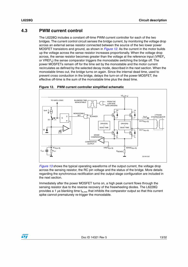
4.3 PWM current controlThe L6228Q includes a constant off-time PWM current controller for each of the two bridges. The current control circuit senses the bridge current, by monitoring the voltage drop across an external sense resistor connected between the source of the two lower power MOSFET transistors and ground, as shown in Figure 12. As the current in the motor builds up the voltage across the sense resistor increases proportionally. When the voltage drop across, the sense resistor becomes greater than the voltage at the reference input (VREFA or VREFB) the sense comparator triggers the monostable switching the bridge off. The power MOSFETs remain off for the time set by the monostable and the motor current recirculates as defined by the selected decay mode, described in the next section. When the monostable times out, the bridge turns on again. Since the internal dead time, used to prevent cross conduction in the bridge, delays the turn-on of the power MOSFET, the effective off-time is the sum of the monostable time plus the dead time.
Figure 12. PWM current controller simplified schematic
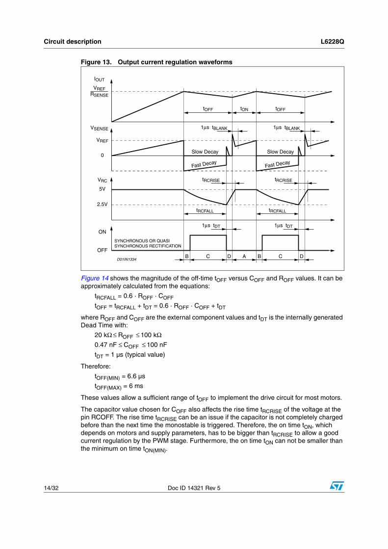
Figure 13 shows the typical operating waveforms of the output current, the voltage drop across the sensing resistor, the RC pin voltage and the status of the bridge. More details regarding the synchronous rectification and the output stage configuration are included in the next section.
Immediately after the power MOSFET turns on, a high peak current flows through the sensing resistor due to the reverse recovery of the freewheeling diodes. The L6228Q provides a 1 μs blanking time tBLANK that inhibits the comparator output so that this current spike cannot prematurely re-trigger the monostable.
DRIVERS+
DEAD TIME
SQ
R
DRIVERS+
DEAD TIME
2H 1H
2L 1L
OUT2A(or B)
SENSEA(or B)
RSENSE
D01IN1332
RCA(or B)
ROFFCOFF
VREFA(or B)
IOUT
OUT1A(or B)
+
+
-
-
1μs
5mA
BLANKER
SENSECOMPARATOR
COMPARATOROUTPUT
MONOSTABLESET
2.5V
5V
FROM THELOW-SIDE
GATE DRIVERS
2 PHASESTEPPER MOTOR
BLANKING TIMEMONOSTABLE
VSA (or B)
TO GATE LOGIC
(0) (1)
Circuit description L6228Q
14/32 Doc ID 14321 Rev 5
Figure 13. Output current regulation waveforms
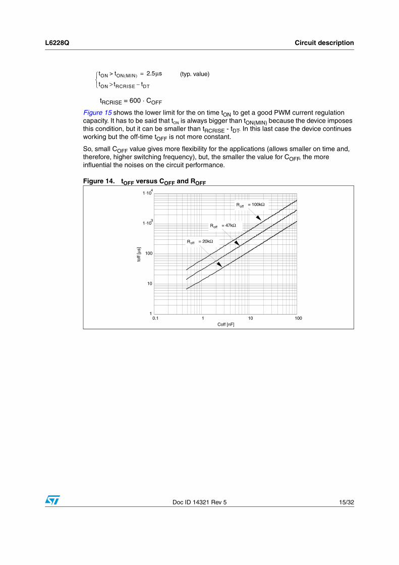
Figure 14 shows the magnitude of the off-time tOFF versus COFF and ROFF values. It can be approximately calculated from the equations:
tRCFALL = 0.6 · ROFF · COFF
tOFF = tRCFALL + tDT = 0.6 · ROFF · COFF + tDT
where ROFF and COFF are the external component values and tDT is the internally generated Dead Time with:
20 kΩ ≤ ROFF ≤ 100 kΩ0.47 nF ≤ COFF ≤ 100 nF
tDT = 1 µs (typical value)
Therefore:
tOFF(MIN) = 6.6 µs
tOFF(MAX) = 6 ms
These values allow a sufficient range of tOFF to implement the drive circuit for most motors.
The capacitor value chosen for COFF also affects the rise time tRCRISE of the voltage at the pin RCOFF. The rise time tRCRISE can be an issue if the capacitor is not completely charged before than the next time the monostable is triggered. Therefore, the on time tON, which depends on motors and supply parameters, has to be bigger than tRCRISE to allow a good current regulation by the PWM stage. Furthermore, the on time tON can not be smaller than the minimum on time tON(MIN).
OFFB C D DA
tON tOFFtOFF
B C
ON
2.5V
0
Fast DecayFast Decay
Slow Decay Slow Decay
1μs tBLANK
tRCRISE
1μs tDT 1μs tDT
tRCRISE
tRCFALLtRCFALL
SYNCHRONOUS OR QUASISYNCHRONOUS RECTIFICATION
1μs tBLANK
5V
VRC
VSENSE
VREF
IOUT
VREFRSENSE
D01IN1334
L6228Q Circuit description
Doc ID 14321 Rev 5 15/32
tRCRISE = 600 · COFF
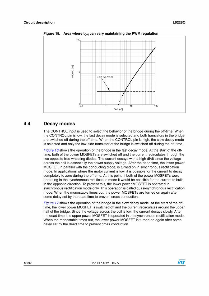
Figure 15 shows the lower limit for the on time tON to get a good PWM current regulation capacity. It has to be said that tON is always bigger than tON(MIN) because the device imposes this condition, but it can be smaller than tRCRISE - tDT. In this last case the device continues working but the off-time tOFF is not more constant.
So, small COFF value gives more flexibility for the applications (allows smaller on time and, therefore, higher switching frequency), but, the smaller the value for COFF, the more influential the noises on the circuit performance.
Figure 14. tOFF versus COFF and ROFF
tON tON MIN( )> 2.5μs=
tON tRCRISE tDT–>⎩ ⎭⎨ ⎬⎧ ⎫ (typ. value)
0.1 1 10 1001
10
100
1.103
1.104
Coff [nF]
toff
[μs]
Roff = 100kΩ
Roff = 47kΩ
Roff = 20kΩ
Circuit description L6228Q
16/32 Doc ID 14321 Rev 5
Figure 15. Area where tON can vary maintaining the PWM regulation
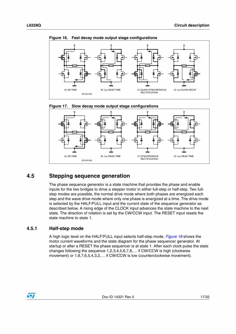
4.4 Decay modesThe CONTROL input is used to select the behavior of the bridge during the off-time. When the CONTROL pin is low, the fast decay mode is selected and both transistors in the bridge are switched off during the off-time. When the CONTROL pin is high, the slow decay mode is selected and only the low-side transistor of the bridge is switched off during the off-time.
Figure 16 shows the operation of the bridge in the fast decay mode. At the start of the off-time, both of the power MOSFETs are switched off and the current recirculates through the two opposite free wheeling diodes. The current decays with a high dI/dt since the voltage across the coil is essentially the power supply voltage. After the dead time, the lower power MOSFET, in parallel with the conducting diode, is turned on in synchronous rectification mode. In applications where the motor current is low, it is possible for the current to decay completely to zero during the off-time. At this point, if both of the power MOSFETs were operating in the synchronous rectification mode it would be possible for the current to build in the opposite direction. To prevent this, the lower power MOSFET is operated in synchronous rectification mode only. This operation is called quasi-synchronous rectification mode. When the monostable times out, the power MOSFETs are turned on again after some delay set by the dead time to prevent cross conduction.
Figure 17 shows the operation of the bridge in the slow decay mode. At the start of the off-time, the lower power MOSFET is switched off and the current recirculates around the upper half of the bridge. Since the voltage across the coil is low, the current decays slowly. After the dead time, the upper power MOSFET is operated in the synchronous rectification mode. When the monostable times out, the lower power MOSFET is turned on again after some delay set by the dead time to prevent cross conduction.
0.1 1 10 1001
10
100
Coff [nF]
ton(
min
) [u
s]
2.5μs (typ. value)
L6228Q Circuit description
Doc ID 14321 Rev 5 17/32
Figure 16. Fast decay mode output stage configurations
Figure 17. Slow decay mode output stage configurations
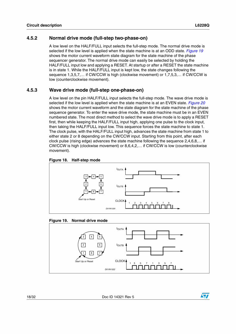
4.5 Stepping sequence generationThe phase sequence generator is a state machine that provides the phase and enable inputs for the two bridges to drive a stepper motor in either full-step or half-step. Two full-step modes are possible, the normal drive mode where both phases are energized each step and the wave drive mode where only one phase is energized at a time. The drive mode is selected by the HALF/FULL input and the current state of the sequence generator as described below. A rising edge of the CLOCK input advances the state machine to the next state. The direction of rotation is set by the CW/CCW input. The RESET input resets the state machine to state 1.
4.5.1 Half-step mode
A high logic level on the HALF/FULL input selects half-step mode. Figure 18 shows the motor current waveforms and the state diagram for the phase sequencer generator. At startup or after a RESET the phase sequencer is at state 1. After each clock pulse the state changes following the sequence 1,2,3,4,5,6,7,8,… if CW/CCW is high (clockwise movement) or 1,8,7,6,5,4,3,2,… if CW/CCW is low (counterclockwise movement).
A) ON TIME B) 1μs DEAD TIME C) QUASI-SYNCHRONOUS RECTIFICATION
D) 1μs SLOW DECAY
D01IN1335
A) ON TIME B) 1μs DEAD TIME C) SYNCHRONOUS RECTIFICATION
D) 1μs DEAD TIME
D01IN1336
Circuit description L6228Q
18/32 Doc ID 14321 Rev 5
4.5.2 Normal drive mode (full-step two-phase-on)
A low level on the HALF/FULL input selects the full-step mode. The normal drive mode is selected if the low level is applied when the state machine is at an ODD state. Figure 19 shows the motor current waveform state diagram for the state machine of the phase sequencer generator. The normal drive mode can easily be selected by holding the HALF/FULL input low and applying a RESET. At startup or after a RESET the state machine is in state 1. While the HALF/FULL input is kept low, the state changes following the sequence 1,3,5,7,… if CW/CCW is high (clockwise movement) or 1,7,5,3,… if CW/CCW is low (counterclockwise movement).
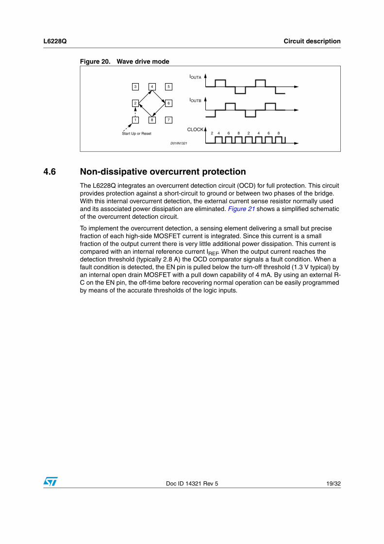
4.5.3 Wave drive mode (full-step one-phase-on)
A low level on the pin HALF/FULL input selects the full-step mode. The wave drive mode is selected if the low level is applied when the state machine is at an EVEN state. Figure 20 shows the motor current waveform and the state diagram for the state machine of the phase sequence generator. To enter the wave drive mode, the state machine must be in an EVEN numbered state. The most direct method to select the wave drive mode is to apply a RESET first, then while keeping the HALF/FULL input high, applying one pulse to the clock input, then taking the HALF/FULL input low. This sequence forces the state machine to state 1. The clock pulse, with the HALF/FULL input high, advances the state machine from state 1 to either state 2 or 8 depending on the CW/CCW input. Starting from this point, after each clock pulse (rising edge) advances the state machine following the sequence 2,4,6,8,… if CW/CCW is high (clockwise movement) or 8,6,4,2,… if CW/CCW is low (counterclockwise movement).
Figure 18. Half-step mode
Figure 19. Normal drive mode
3
2
4 5
1
D01IN1320
2 3 4 5 6 7 8
6
1 8 7
IOUTA
IOUTB
CLOCKStart Up or Reset
2
4
1
D01IN1322
3 5 7 1 3 5 7
6
8
IOUTA
IOUTB
CLOCK
3 5
1 7
Start Up or Reset
L6228Q Circuit description
Doc ID 14321 Rev 5 19/32
Figure 20. Wave drive mode
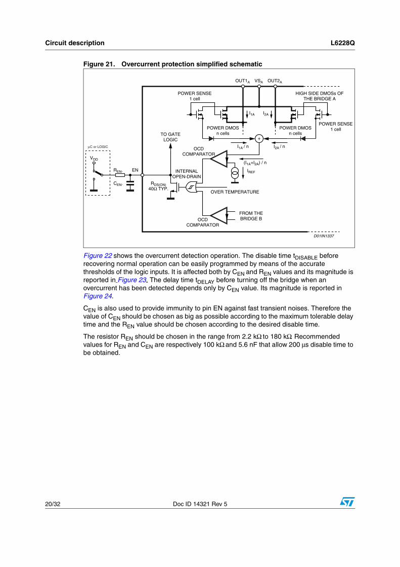
4.6 Non-dissipative overcurrent protectionThe L6228Q integrates an overcurrent detection circuit (OCD) for full protection. This circuit provides protection against a short-circuit to ground or between two phases of the bridge. With this internal overcurrent detection, the external current sense resistor normally used and its associated power dissipation are eliminated. Figure 21 shows a simplified schematic of the overcurrent detection circuit.
To implement the overcurrent detection, a sensing element delivering a small but precise fraction of each high-side MOSFET current is integrated. Since this current is a small fraction of the output current there is very little additional power dissipation. This current is compared with an internal reference current IREF. When the output current reaches the detection threshold (typically 2.8 A) the OCD comparator signals a fault condition. When a fault condition is detected, the EN pin is pulled below the turn-off threshold (1.3 V typical) by an internal open drain MOSFET with a pull down capability of 4 mA. By using an external R-C on the EN pin, the off-time before recovering normal operation can be easily programmed by means of the accurate thresholds of the logic inputs.
2
4
2
D01IN1321
4 6 8 2 4 6 8
6
8
IOUTA
IOUTB
CLOCK
3 5
1 7
Start Up or Reset
Circuit description L6228Q
20/32 Doc ID 14321 Rev 5
Figure 21. Overcurrent protection simplified schematic
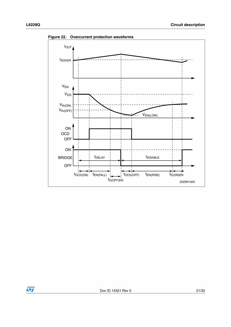
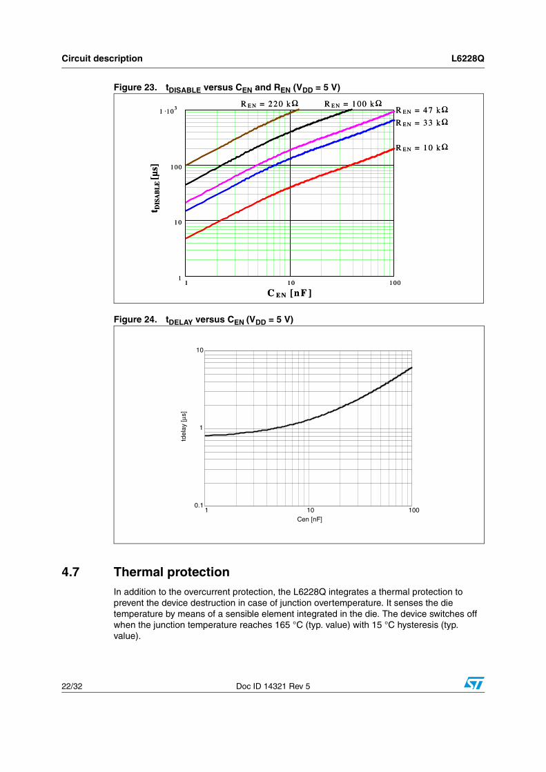
Figure 22 shows the overcurrent detection operation. The disable time tDISABLE before recovering normal operation can be easily programmed by means of the accurate thresholds of the logic inputs. It is affected both by CEN and REN values and its magnitude is reported in Figure 23. The delay time tDELAY before turning off the bridge when an overcurrent has been detected depends only by CEN value. Its magnitude is reported in Figure 24.
CEN is also used to provide immunity to pin EN against fast transient noises. Therefore the value of CEN should be chosen as big as possible according to the maximum tolerable delay time and the REN value should be chosen according to the desired disable time.
The resistor REN should be chosen in the range from 2.2 kΩ to 180 kΩ. Recommended values for REN and CEN are respectively 100 kΩ and 5.6 nF that allow 200 μs disable time to be obtained.
+
OVER TEMPERATURE
IREF
(I1A+I2A) / n
I1A / n
POWER SENSE1 cell
POWER SENSE1 cellPOWER DMOS
n cellsPOWER DMOS
n cells
HIGH SIDE DMOSs OFTHE BRIDGE A
OUT1A OUT2A VSA
I1A I2A
I2A / n
FROM THEBRIDGE BOCD
COMPARATOR
OCDCOMPARATOR
TO GATELOGIC
INTERNALOPEN-DRAIN
RDS(ON)40Ω TYP.
CEN.
REN. EN
VDD
μC or LOGIC
D01IN1337
L6228Q Circuit description
Doc ID 14321 Rev 5 21/32
Figure 22. Overcurrent protection waveforms
ISOVER
IOUT
Vth(ON)
Vth(OFF)VEN(LOW)
VDD
tOCD(ON) tD(ON)ENtEN(FALL) tEN(RISE)
tDISABLEtDELAY
tOCD(OFF)
tD(OFF)EN
VEN
BRIDGE
ON
OFF
OCDON
OFF
D02IN1400
Circuit description L6228Q
22/32 Doc ID 14321 Rev 5
Figure 23. tDISABLE versus CEN and REN (VDD = 5 V)
Figure 24. tDELAY versus CEN (VDD = 5 V)
4.7 Thermal protectionIn addition to the overcurrent protection, the L6228Q integrates a thermal protection to prevent the device destruction in case of junction overtemperature. It senses the die temperature by means of a sensible element integrated in the die. The device switches off when the junction temperature reaches 165 °C (typ. value) with 15 °C hysteresis (typ. value).
1 10 1 001
1 0
1 00
1 .103
C E N [n F ]
t DIS
AB
LE
[µs]
R E N = 220 k Ω R E N = 1 00 k ΩR E N = 47 k ΩR E N = 33 k Ω
R E N = 10 k Ω
1 10 1 001
1 0
1 00
1 .103
C E N [n F ]
t DIS
AB
LE
[µs]
R E N = 220 k Ω R E N = 1 00 k ΩR E N = 47 k ΩR E N = 33 k Ω
R E N = 10 k Ω
1 10 1000.1
1
10
Cen [nF]
tdel
ay [μ
s]
L6228Q Application information
Doc ID 14321 Rev 5 23/32
5 Application information
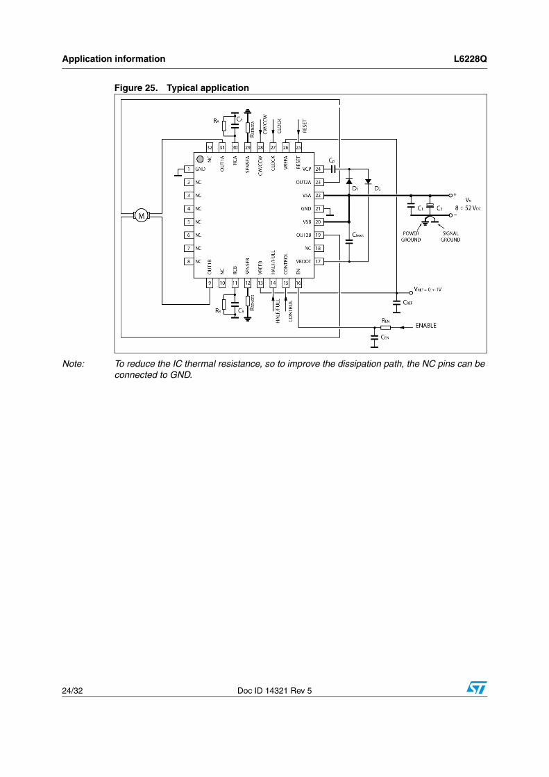
A typical bipolar stepper motor driver application using L6228Q is shown in Figure 25. Typical component values for the application are shown in Table 7. A high quality ceramic capacitor in the range from 100 to 200 nF should be placed between the power pins (VSA and VSB) and ground near the L6228Q to improve the high frequency filtering on the power supply and to reduce high frequency transients generated by the switching. The capacitor connected from the EN input to ground sets the shut down time when an overcurrent is detected (see overcurrent protection). The two current sensing inputs (SENSEA and SENSEB) should be connected to the sensing resistors with a trace length as short as possible in the layout. The sense resistors should be non-inductive resistors to minimize the dI/dt transients across the resistor. To increase noise immunity, unused logic pins (except EN) are connected to 5 V (high logic level) or GND (low logic level) (see pin description). It is recommended power ground and signal ground to be separated on PCB.
Table 7. Component values for typical application
Component Value
C1 100 µF
C2 100 nF
CA 1 nF
CB 1 nF
CBOOT 220 nF
CP 10 nF
CEN 5.6 nF
CREF 68 nF
D1 1N4148
D2 1N4148
RA 39 kΩ
RB 39 kΩ
REN 100 kΩ
RSENSEA 0.6 Ω
RSENSEB 0.6 Ω
Application information L6228Q
24/32 Doc ID 14321 Rev 5
Figure 25. Typical application
Note: To reduce the IC thermal resistance, so to improve the dissipation path, the NC pins can be connected to GND.
L6228Q Output current capability and IC power dissipation
Doc ID 14321 Rev 5 25/32
6 Output current capability and IC power dissipation
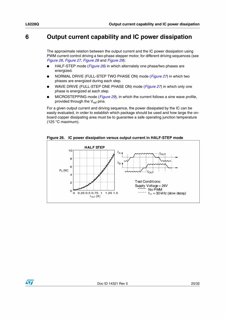
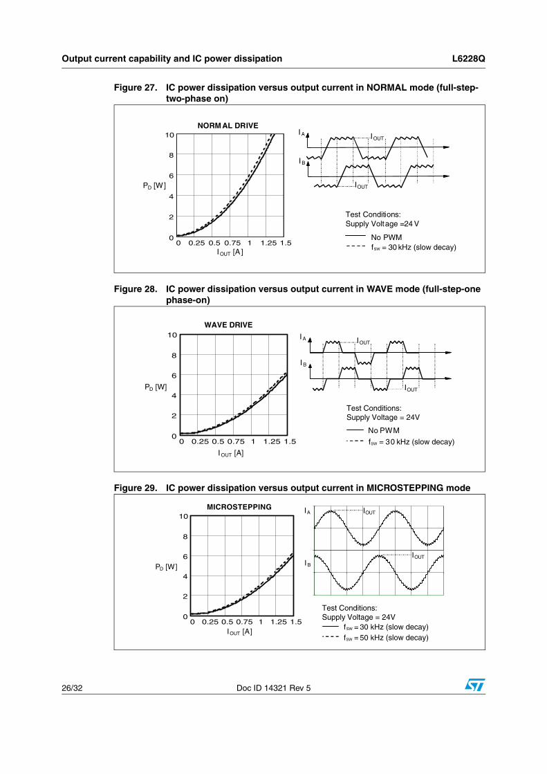
The approximate relation between the output current and the IC power dissipation using PWM current control driving a two-phase stepper motor, for different driving sequences (see Figure 26, Figure 27, Figure 28 and Figure 29):
● HALF-STEP mode (Figure 26) in which alternately one phase/two phases are energized.
● NORMAL DRIVE (FULL-STEP TWO PHASE ON) mode (Figure 27) in which two phases are energized during each step.
● WAVE DRIVE (FULL-STEP ONE PHASE ON) mode (Figure 27) in which only one phase is energized at each step.
● MICROSTEPPING mode (Figure 29), in which the current follows a sine wave profile, provided through the Vref pins.
For a given output current and driving sequence, the power dissipated by the IC can be easily evaluated, in order to establish which package should be used and how large the on-board copper dissipating area must be to guarantee a safe operating junction temperature (125 °C maximum).
Figure 26. IC power dissipation versus output current in HALF-STEP mode
No PWM fSW = 30 kHz (slow decay)
Test Conditions: Supply Voltage = 24V
IA
IB
IOUT
IOUT PD [W]
IOUT [A]
HALF STEP
0 0.25 0.5 0.75 1 1.25 1.50
2
4
6
8
10
Output current capability and IC power dissipation L6228Q
26/32 Doc ID 14321 Rev 5
Figure 27. IC power dissipation versus output current in NORMAL mode (full-step- two-phase on)
Figure 28. IC power dissipation versus output current in WAVE mode (full-step-one phase-on)
Figure 29. IC power dissipation versus output current in MICROSTEPPING mode
No PWMfSW = 30 kHz (slow decay)
Test Conditions:Supply Voltage = 24 V
IA
IB
IOUT
IOUTPD [W]
IOUT [A]
NORM AL DRIVE
0 0.25 0.5 0.75 1 1.25 1.50
2
4
6
8
10
No PWM
fSW = 30 kHz (slow decay)
Test Conditions:Supply Voltage = 24V
IA
IB
IOUT
IOUT
WAVE DRIVE
PD [W]
IOUT [A]
0 0.25 0.5 0.75 1 1.25 1.50
2
4
6
8
10
fSW = 50 kHz (slow decay)fSW = 30 kHz (slow decay)
IA
I B
IOUT
IOUT
MICROSTEPPING
PD [W]
IOUT [A]
Test Conditions:Supply Voltage = 24V
0 0.25 0.5 0.75 1 1.25 1.50
2
4
6
8
10
L6228Q Thermal management
Doc ID 14321 Rev 5 27/32
7 Thermal management
In most applications the power dissipation in the IC is the main factor that sets the maximum current that can be delivered by the device in a safe operating condition. Therefore, it has to be taken into account very carefully. Besides, the available space on the PCB, the right package should be chosen considering the power dissipation. Heat sinking can be achieved using copper on the PCB with proper area and thickness.
For instance, using a VFQFPN32L 5x5 package the typical Rth(JA) is about 42 °C/W when mounted on a double-layer FR4 PCB with a dissipating copper surface of 0.5 cm2 on the top side plus 6 cm2 ground layer connected through 18 via holes (9 below the IC).
Package mechanical data L6228Q
28/32 Doc ID 14321 Rev 5
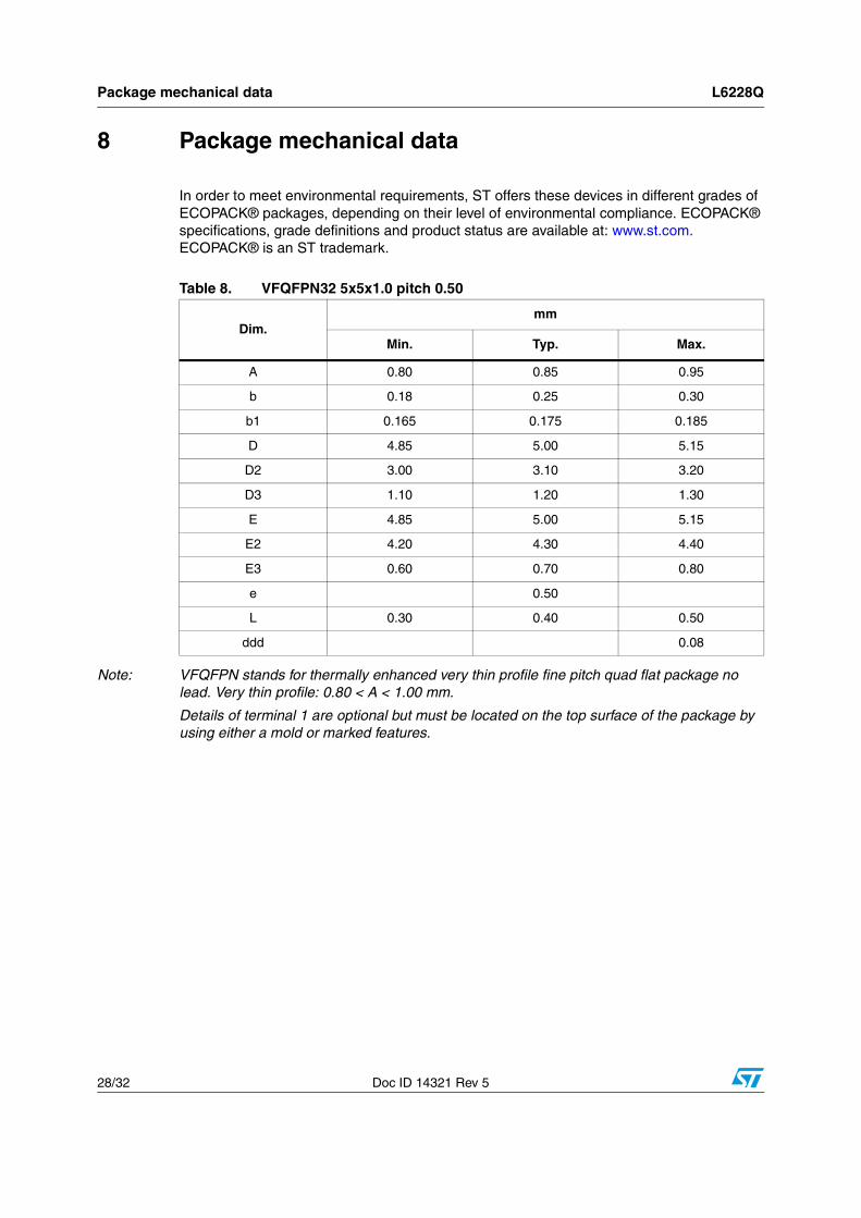
8 Package mechanical data
In order to meet environmental requirements, ST offers these devices in different grades of ECOPACK® packages, depending on their level of environmental compliance. ECOPACK® specifications, grade definitions and product status are available at: www.st.com. ECOPACK® is an ST trademark.
Note: VFQFPN stands for thermally enhanced very thin profile fine pitch quad flat package no lead. Very thin profile: 0.80 < A < 1.00 mm.
Details of terminal 1 are optional but must be located on the top surface of the package by using either a mold or marked features.
Table 8. VFQFPN32 5x5x1.0 pitch 0.50
Dim. mm
Min. Typ. Max.
A 0.80 0.85 0.95
b 0.18 0.25 0.30
b1 0.165 0.175 0.185
D 4.85 5.00 5.15
D2 3.00 3.10 3.20
D3 1.10 1.20 1.30
E 4.85 5.00 5.15
E2 4.20 4.30 4.40
E3 0.60 0.70 0.80
e 0.50
L 0.30 0.40 0.50
ddd 0.08
L6228Q Package mechanical data
Doc ID 14321 Rev 5 29/32
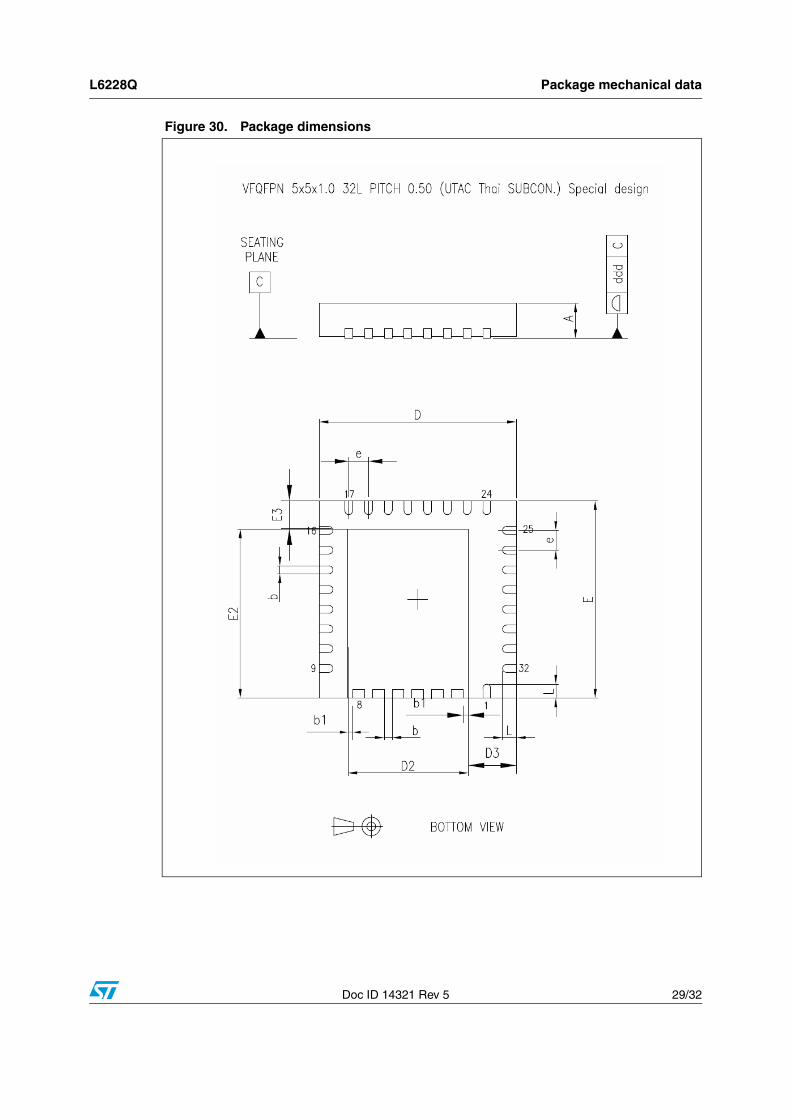
Figure 30. Package dimensions
Ordering information L6228Q
30/32 Doc ID 14321 Rev 5
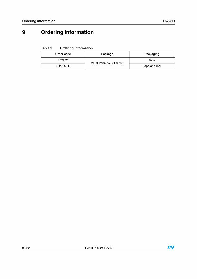
9 Ordering information
Table 9. Ordering information
Order code Package Packaging
L6228QVFQFPN32 5x5x1.0 mm
Tube
L6228QTR Tape and reel
L6228Q Revision history
Doc ID 14321 Rev 5 31/32
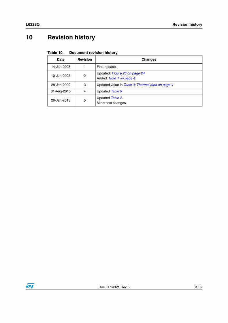
10 Revision history
Table 10. Document revision history
Date Revision Changes
14-Jan-2008 1 First release.
10-Jun-2008 2Updated: Figure 25 on page 24Added: Note 1 on page 4
28-Jan-2009 3 Updated value in Table 3: Thermal data on page 4
31-Aug-2010 4 Updated Table 9
28-Jan-2013 5Updated Table 2.Minor text changes.
L6228Q
32/32 Doc ID 14321 Rev 5
Please Read Carefully:
Information in this document is provided solely in connection with ST products. STMicroelectronics NV and its subsidiaries (“ST”) reserve theright to make changes, corrections, modifications or improvements, to this document, and the products and services described herein at anytime, without notice.
All ST products are sold pursuant to ST’s terms and conditions of sale.
Purchasers are solely responsible for the choice, selection and use of the ST products and services described herein, and ST assumes noliability whatsoever relating to the choice, selection or use of the ST products and services described herein.
No license, express or implied, by estoppel or otherwise, to any intellectual property rights is granted under this document. If any part of thisdocument refers to any third party products or services it shall not be deemed a license grant by ST for the use of such third party productsor services, or any intellectual property contained therein or considered as a warranty covering the use in any manner whatsoever of suchthird party products or services or any intellectual property contained therein.
UNLESS OTHERWISE SET FORTH IN ST’S TERMS AND CONDITIONS OF SALE ST DISCLAIMS ANY EXPRESS OR IMPLIEDWARRANTY WITH RESPECT TO THE USE AND/OR SALE OF ST PRODUCTS INCLUDING WITHOUT LIMITATION IMPLIEDWARRANTIES OF MERCHANTABILITY, FITNESS FOR A PARTICULAR PURPOSE (AND THEIR EQUIVALENTS UNDER THE LAWSOF ANY JURISDICTION), OR INFRINGEMENT OF ANY PATENT, COPYRIGHT OR OTHER INTELLECTUAL PROPERTY RIGHT.
UNLESS EXPRESSLY APPROVED IN WRITING BY TWO AUTHORIZED ST REPRESENTATIVES, ST PRODUCTS ARE NOTRECOMMENDED, AUTHORIZED OR WARRANTED FOR USE IN MILITARY, AIR CRAFT, SPACE, LIFE SAVING, OR LIFE SUSTAININGAPPLICATIONS, NOR IN PRODUCTS OR SYSTEMS WHERE FAILURE OR MALFUNCTION MAY RESULT IN PERSONAL INJURY,DEATH, OR SEVERE PROPERTY OR ENVIRONMENTAL DAMAGE. ST PRODUCTS WHICH ARE NOT SPECIFIED AS "AUTOMOTIVEGRADE" MAY ONLY BE USED IN AUTOMOTIVE APPLICATIONS AT USER’S OWN RISK.
Resale of ST products with provisions different from the statements and/or technical features set forth in this document shall immediately voidany warranty granted by ST for the ST product or service described herein and shall not create or extend in any manner whatsoever, anyliability of ST.
ST and the ST logo are trademarks or registered trademarks of ST in various countries.
Information in this document supersedes and replaces all information previously supplied.
The ST logo is a registered trademark of STMicroelectronics. All other names are the property of their respective owners.
© 2013 STMicroelectronics - All rights reserved
STMicroelectronics group of companies
Australia - Belgium - Brazil - Canada - China - Czech Republic - Finland - France - Germany - Hong Kong - India - Israel - Italy - Japan - Malaysia - Malta - Morocco - Philippines - Singapore - Spain - Sweden - Switzerland - United Kingdom - United States of America
www.st.com