LTC6954 - Low Phase Noise, Triple Output Clock ...cds.linear.com/docs/en/datasheet/6954f.pdf ·...
56
LTC6954 1 6954f For more information www.linear.com/LTC6954 TYPICAL APPLICATION FEATURES DESCRIPTION Low Phase Noise, Triple Output Clock Distribution Divider/Driver The LTC ® 6954 is a family of very low phase noise clock distribution parts. Each part has three outputs and each output has an individually programmable frequency divider and delay. There are four members of the family, differing in their output logic signal type: LTC6954-1: Three LVPECL outputs LTC6954-2: Two LVPECL and one LVDS/CMOS outputs LTC6954-3: One LVPECL and two LVDS/CMOS outputs LTC6954-4: Three LVDS/CMOS outputs Each output is individually programmable to divide the input frequency by any integer from 1 to 63, and to delay each output by 0 to 63 input clock cycles. The output duty cycle is always 50%, regardless of the divide number. The LVDS/CMOS outputs are jumper selectable via the OUTxSEL pins to provide either an LVDS logic output or a CMOS logic output. The LTC6954 also features Linear Technology’s EZSync system for perfect clock synchronization and alignment every time. All device settings are controlled through an SPI-compatible serial port. Additive Phase Noise vs Offset Frequency, f IN = 622.08MHz, Mx[5:0] = 4, f OUTx = 155.52MHz APPLICATIONS n Low Noise Clock Distribution: Suitable for High Speed/High Resolution ADC Clocking n Additive Jitter < 20fs RMS (12kHz to 20MHz) n Additive Jitter < 85fs RMS (10Hz to Nyquist) n 1.8GHz Maximum Input Frequency (LTC6954-1 When DELAY = 0) n 1.4GHz Maximum Input Frequency (LTC6954-1 When DELAY > 0, LTC6954-2, -3, -4) n EZSync™ Clock Synchronization Compatible n Three Independent, Low Noise Outputs n Four Output Combinations Available n Three Independent Programmable Dividers Covering All Integers From 1 to 63 n Three Independent Programmable Delays Covering All Integers From 0 to 63 n –40°C to 105°C Junction Temperature Range n Clocking High Speed, High Resolution ADCs, DACs and Data Acquisition Systems n Low Jitter Clock Distribution L, LT, LTC, LTM, Linear Technology and the Linear logo are registered trademarks and EZSync is a trademark of Linear Technology Corporation. All other trademarks are the property of their respective owners. Protected by U.S. Patents, including 8319551, 8819472. 6954 TA01a LVPECL OUTPUT FREQUENCY UP TO 1.8GHz LVDS OUTPUT FREQUENCY UP TO 1.4GHz CMOS OUTPUT FREQUENCY UP TO 250MHz OUT2 + OUT2 – DIVIDE 1 TO 63 DELAY 0 TO 63 OUT1 + OUT1 – DIVIDE 1 TO 63 DELAY 0 TO 63 OUT0 + OUT0 – SPI SERIAL PORT DIVIDE 1 TO 63 DELAY 0 TO 63 V + 3.3V 0.1μF 3.3V SCLK CS GND SDO SDI OUT0SEL OUT1SEL OUT2SEL SYNC IN + IN – LTC6954-3 UP TO 1.4GHz 49.9Ω 49.9Ω 49.9Ω SYNC CONTROL SERIAL PORT AND DIGITAL –180 ADDITIVE PHASE NOISE (dBc/Hz) –160 –150 –130 –120 –170 –140 6954 TA01b OFFSET FREQUENCY (Hz) 10 100 1k 1M 10M 100k 10k
Transcript of LTC6954 - Low Phase Noise, Triple Output Clock ...cds.linear.com/docs/en/datasheet/6954f.pdf ·...
LTC6954
16954f
For more information www.linear.com/LTC6954
Typical applicaTion
FeaTures DescripTion
Low Phase Noise, Triple Output Clock
Distribution Divider/Driver
The LTC®6954 is a family of very low phase noise clock distribution parts. Each part has three outputs and each output has an individually programmable frequency divider and delay. There are four members of the family, differing in their output logic signal type: LTC6954-1: Three LVPECL outputsLTC6954-2: Two LVPECL and one LVDS/CMOS outputsLTC6954-3: One LVPECL and two LVDS/CMOS outputsLTC6954-4: Three LVDS/CMOS outputs
Each output is individually programmable to divide the input frequency by any integer from 1 to 63, and to delay each output by 0 to 63 input clock cycles. The output duty cycle is always 50%, regardless of the divide number. The LVDS/CMOS outputs are jumper selectable via the OUTxSEL pins to provide either an LVDS logic output or a CMOS logic output.
The LTC6954 also features Linear Technology’s EZSync system for perfect clock synchronization and alignment every time.
All device settings are controlled through an SPI-compatible serial port.
Additive Phase Noise vs Offset Frequency, fIN = 622.08MHz, Mx[5:0] = 4,
fOUTx = 155.52MHz
applicaTions
n Low Noise Clock Distribution: Suitable for High Speed/High Resolution ADC Clocking
n Additive Jitter < 20fsRMS (12kHz to 20MHz)n Additive Jitter < 85fsRMS (10Hz to Nyquist)n 1.8GHz Maximum Input Frequency (LTC6954-1 When DELAY = 0)n 1.4GHz Maximum Input Frequency (LTC6954-1 When DELAY > 0, LTC6954-2, -3, -4)n EZSync™ Clock Synchronization Compatiblen Three Independent, Low Noise Outputsn Four Output Combinations Availablen Three Independent Programmable Dividers Covering
All Integers From 1 to 63n Three Independent Programmable Delays Covering
All Integers From 0 to 63n –40°C to 105°C Junction Temperature Range
n Clocking High Speed, High Resolution ADCs, DACs and Data Acquisition Systems
n Low Jitter Clock DistributionL, LT, LTC, LTM, Linear Technology and the Linear logo are registered trademarks and EZSync is a trademark of Linear Technology Corporation. All other trademarks are the property of their respective owners. Protected by U.S. Patents, including 8319551, 8819472.
6954 TA01a
LVPECL OUTPUTFREQUENCYUP TO 1.8GHz
LVDS OUTPUTFREQUENCYUP TO 1.4GHz
CMOS OUTPUTFREQUENCYUP TO 250MHz
OUT2+
OUT2–DIVIDE1 TO 63
DELAY0 TO 63
OUT1+
OUT1–DIVIDE1 TO 63
DELAY0 TO 63
OUT0+
OUT0–
SPISERIAL
PORT
DIVIDE1 TO 63
DELAY0 TO 63
V+
3.3V0.1µF
3.3V
SCLK
CSGND
SDO
SDI
OUT0SEL
OUT1SEL
OUT2SEL
SYNC
IN+
IN–
LTC6954-3
UP TO 1.4GHz
49.9Ω
49.9Ω49.9Ω
SYNCCONTROL
SERIALPORTAND
DIGITAL
–180
ADDI
TIVE
PHA
SE N
OISE
(dBc
/Hz)
–160
–150
–130
–120
–170
–140
6954 TA01bOFFSET FREQUENCY (Hz)
10 100 1k 1M 10M100k10k
LTC6954
26954f
For more information www.linear.com/LTC6954
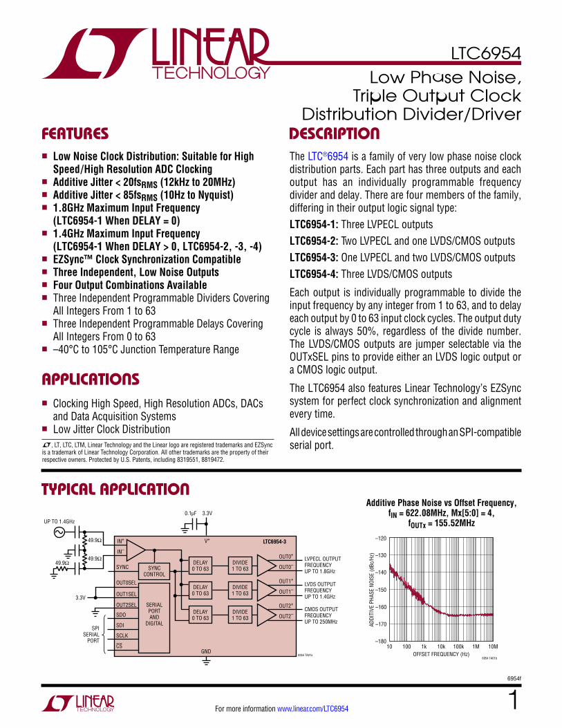
pin conFiguraTionabsoluTe MaxiMuM raTings
Supply Voltages(VA
+, VD+, VIN
+, VOUT0+, VOUT1
+ and VOUT2
+ to GND) ........................................................3.6VLTC6954-1, -2, -3 LVPECL Outputs OUTx Output Voltage High ......................VOUT
+ + 0.3V OUTx Output Voltage Low ..................... Source 25mALTC6954-2, -3, -4 LVDS/CMOS Outputs OUTx ..........................................–0.3V to (VA
+ +0.3V)TEMP Input Current ...............................................10mATEMP Low Voltage ................................................–0.3VVoltage on All Other Pins ..............–0.3V to (VA
+ + 0.3V)Operating Junction Temperature Range, TJ (Note 2)LTC6954I ............................................... –40°C to 105°CJunction Temperature, TJMAX ................................ 150°CStorage Temperature Range .................. –65°C to 150°C
(Note 1)
13 14
TOP VIEW
37GND
UFF PACKAGE36-LEAD (4mm × 7mm) PLASTIC QFN
0.5mm LEAD PITCH
15 16 17 18
36 35 34 33 32 31VOUT2
+
OUT2–
OUT2+
VOUT2+
VOUT1+
OUT1–
OUT1+
VOUT1+
VOUT0+
OUT0–
OUT0+
VOUT0+
VIN+
GND
IN–
IN+
GND
VIN+
VA+
VA+
SYNC
VD+
SDI
SCLK
OUT2
SEL
GND
V A+
OUT1
SEL
GND
TEM
P
OUT0
SEL
GND
V A+
CS
SDO
V D+
22
21
20
19
23
24
25
26
27
28
29
30
8
9
10
11
12
7
6
5
4
3
2
1
TJMAX = 150°C, θJCbottom = 2°C/W, θJCtop = 18°C/W
EXPOSED PAD (PIN 37) IS GND, MUST BE SOLDERED TO PCB GND
orDer inForMaTionLEAD FREE FINISH TAPE AND REEL PART MARKING PACKAGE DESCRIPTION JUNCTION TEMPERATURE RANGE
LTC6954IUFF-1#PBF LTC6954IUFF-1#TRPBF 69541 36-Lead (4mm × 7mm) Plastic QFN –40°C to 105°C
LTC6954IUFF-2#PBF LTC6954IUFF-2#TRPBF 69542 36-Lead (4mm × 7mm) Plastic QFN –40°C to 105°C
LTC6954IUFF-3#PBF LTC6954IUFF-3#TRPBF 69543 36-Lead (4mm × 7mm) Plastic QFN –40°C to 105°C
LTC6954IUFF-4#PBF LTC6954IUFF-4#TRPBF 69544 36-Lead (4mm × 7mm) Plastic QFN –40°C to 105°C
Consult LTC Marketing for parts specified with wider operating temperature ranges.
For more information on lead free part markings, go to: http://www.linear.com/leadfree/ For more information on tape and reel specifications, go to: http://www.linear.com/tapeandreel/. Some packages are available in 500 unit reels through designated sales channels with #TRMPBF suffix.
LTC6954
36954f
For more information www.linear.com/LTC6954
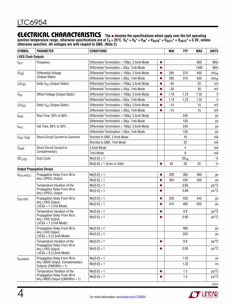
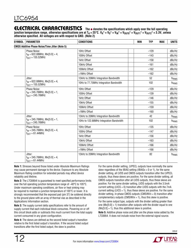
elecTrical characTerisTics
SYMBOL PARAMETER CONDITIONS MIN TYP MAX UNITS
Input (IN+, IN–)
fIN Input Frequency LTC6954-1, DELx = 0 LTC6954-1 (DELx > 0), LTC6954-2, -3, -4
l
l
1800 1400
MHz MHz
VIN Input Signal Level Single-Ended l 0.2 0.8 1.5 VP-P
Input Slew Rate l 100 V/µs
DCIN Input Duty Cycle 50 %
Self-Bias Voltage l 1.9 2.05 2.2 V
Minimum Common Mode Level 400mVP-P Differential Input 1.8 V
Maximum Common Mode Level 400mVP-P Differential Input 2.3 V
Input Resistance Differential l 1.8 2.2 2.7 kΩ
Input Capacitance Differential 0.5 pF
Output Divider (M)
Mx[5:0] Divider Range M0[5:0], M1[5:0], M2[5:0]
All Integers Included l 1 63 Cycles
DELx[5:0] Divider Delay in Input Clock Cycles DEL0[5:0], DEL1[5:0], DEL2[5:0]
All Integers Included l 0 63 Cycles
LVPECL Clock Outputs
fOUT Frequency LTC6954-1, DELx = 0 LTC6954-1 (DELx > 0), LTC6954-2, -3, -4
l
l
1800 1400
MHz MHz
|VOD| Differential Voltage (Output Static)
Single-Ended Termination = 50Ω to (VOUTx+ – 2V) l 640 775 950 mVPK
Differential Termination = 100Ω, Internal Bias On l 640 780 950 mVPK
VCM Common Mode Voltage (Output Static)
Single-Ended Termination = 50Ω to (VOUTx+ – 2V) l VOUTx
+
– 1.67VOUTx
+
– 1.42VOUTx
+
– 1.14V
Differential Termination = 100Ω, Internal Bias On l VOUTx+
– 1.67VOUTx
+
– 1.42VOUTx
+
– 1.14V
tRISE Rise Time, 20% to 80% Single-Ended Termination = 50Ω to (VOUTx+ – 2V) 110 ps
Differential Termination = 100Ω, Internal Bias On 110 ps
tFALL Fall Time, 80% to 20% Single-Ended Termination = 50Ω to (VOUTx+ – 2V) 110 ps
Differential Termination = 100Ω, Internal Bias On 110 ps
DCLVPECL Duty Cycle Mx[5:0] = 1 DCIN %
Mx[5:0] > 1 (Even or Odd) l 45 50 55 %
CMOS Clock Outputs
fOUT Frequency l 250 MHz
VOH High Voltage (Output Static) 2.5mA Load l V+ – 0.4 V
VOL Low Voltage (Output Static) 2.5mA Load l 0.4 V
tRISE Rise Time, 20% to 80% CLOAD = 2pF, CMSINV = 1 200 ps
tFALL Fall Time, 80% to 20% CLOAD = 2pF, CMSINV = 1 170 ps
DCCMOS Duty Cycle Mx[5:0] = 1 DCIN %
Mx[5:0] > 1 (Even or Odd) l 45 50 55 %
The l denotes the specifications which apply over the full operating junction temperature range, otherwise specifications are at TA = 25°C. VA
+ = VD+ = VIN
+ = VOUT0+ = VOUT1
+ = VOUT2+ = 3.3V, unless
otherwise specified. All voltages are with respect to GND. (Note 2)
LTC6954
46954f
For more information www.linear.com/LTC6954
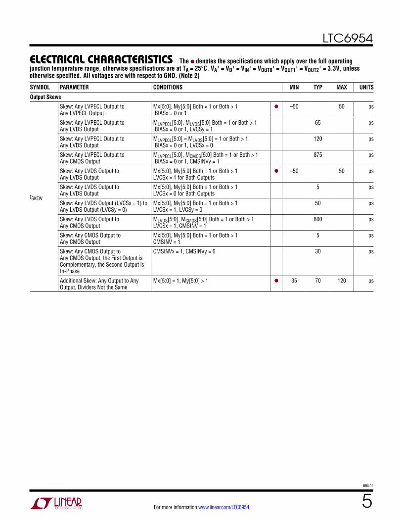
elecTrical characTerisTics The l denotes the specifications which apply over the full operating junction temperature range, otherwise specifications are at TA = 25°C. VA
+ = VD+ = VIN
+ = VOUT0+ = VOUT1
+ = VOUT2+ = 3.3V, unless
otherwise specified. All voltages are with respect to GND. (Note 2)
SYMBOL PARAMETER CONDITIONS MIN TYP MAX UNITS
LVDS Clock Outputs
fOUT Frequency Differential Termination = 100Ω, 3.5mA Mode l 800 MHzDifferential Termination = 50Ω, 7mA Mode l 1400 MHz
|VOD| Differential Voltage (Output Static)
Differential Termination = 100Ω, 3.5mA Mode l 290 370 450 mVPK
Differential Termination = 50Ω, 7mA Mode l 290 370 450 mVPK
|ΔVOD| Delta VOD (Output Static) Differential Termination = 100Ω, 3.5mA Mode l –30 30 mVDifferential Termination = 50Ω, 7mA Mode l –30 30 mV
VOS Offset Voltage (Output Static) Differential Termination = 100Ω, 3.5mA Mode l 1.16 1.23 1.32 VDifferential Termination = 50Ω, 7mA Mode l 1.15 1.23 1.32 V
|ΔVOS| Delta VOS (Output Static) Differential Termination = 100Ω, 3.5mA Mode l –15 15 mVDifferential Termination = 50Ω, 7mA Mode l –15 15 mV
tRISE Rise Time, 20% to 80% Differential Termination = 100Ω, 3.5mA Mode 240 psDifferential Termination = 50Ω, 7mA Mode 120 ps
tFALL Fall Time, 80% to 20% Differential Termination = 100Ω, 3.5mA Mode 240 psDifferential Termination = 50Ω, 7mA Mode 120 ps
|ISA|, |ISB| Short-Circuit Current to Common Shorted to GND, 3.5mA Mode 16 mAShorted to GND, 7mA Mode 25 mA
|ISAB| Short-Circuit Current to Complementary
3.5mA Mode 4 mA7mA Mode 8 mA
DCLVDS Duty Cycle Mx[5:0] = 1 DCIN %Mx[5:0] > 1 (Even or Odd) l 45 50 55 %
Output Propagation Delays
tPD(LVPECL) Propagation Delay From IN to Any LVPECL Output
Mx[5:0] = 1 l 290 360 480 psMx[5:0] > 1 l 360 430 550 ps
Temperature Variation of the Propagation Delay From IN to Any LVPECL Output
Mx[5:0] = 1 l 0.65 ps/°CMx[5:0] > 1 l 0.68 ps/°C
tpd(LVDS) Propagation Delay From IN to Any LVDS Output, LVCSx = 1 (7mA Mode)
Mx[5:0] = 1 l 350 420 545 ps
Mx[5:0] > 1 l 415 480 625 ps
Temperature Variation of the Propagation Delay From IN to Any LVDS Output, LVCSx = 1 (7mA Mode)
Mx[5:0] = 1 l 0.8 ps/°C
Mx[5:0] > 1 l 0.85 ps/°C
Propagation Delay From IN to Any LVDS Output, LVCSx = 0 (3.5mA Mode)
Mx[5:0] = 1 480 ps
Mx[5:0] > 1 550 ps
Temperature Variation of the Propagation Delay From IN to Any LVDS Output, LVCSx = 0 (3.5mA Mode)
Mx[5:0] = 1 l 0.8 ps/°C
Mx[5:0] > 1 l 0.85 ps/°C
tpd(CMOS) Propagation Delay From IN to Any CMOS Output, Complementary Outputs (CMSINVx = 1)
Mx[5:0] = 1 1.25 ns
Mx[5:0] > 1 1.32 ns
Temperature Variation of the Propagation Delay From IN to Any CMOS Output (CMSINVx = 1)
Mx[5:0] = 1 l 1.3 ps/°CMx[5:0] > 1 l 1.4 ps/°C
LTC6954
56954f
For more information www.linear.com/LTC6954
elecTrical characTerisTics The l denotes the specifications which apply over the full operating junction temperature range, otherwise specifications are at TA = 25°C. VA
+ = VD+ = VIN
+ = VOUT0+ = VOUT1
+ = VOUT2+ = 3.3V, unless
otherwise specified. All voltages are with respect to GND. (Note 2)
SYMBOL PARAMETER CONDITIONS MIN TYP MAX UNITS
Output Skews
tSKEW
Skew: Any LVPECL Output to Any LVPECL Output
Mx[5:0], My[5:0] Both = 1 or Both > 1 IBIASx = 0 or 1
l –50 50 ps
Skew: Any LVPECL Output to Any LVDS Output
MLVPECL[5:0], MLVDS[5:0] Both = 1 or Both > 1 IBIASx = 0 or 1, LVCSy = 1
65 ps
Skew: Any LVPECL Output to Any LVDS Output
MLVPECL[5:0] = MLVDS[5:0] = 1 or Both > 1 IBIASx = 0 or 1, LVCSx = 0
120 ps
Skew: Any LVPECL Output to Any CMOS Output
MLVPECL[5:0], MCMOS[5:0] Both = 1 or Both > 1 IBIASx = 0 or 1, CMSINVy = 1
875 ps
Skew: Any LVDS Output to Any LVDS Output
Mx[5:0], My[5:0] Both = 1 or Both > 1 LVCSx = 1 for Both Outputs
l –50 50 ps
Skew: Any LVDS Output to Any LVDS Output
Mx[5:0], My[5:0] Both = 1 or Both > 1 LVCSx = 0 for Both Outputs
5 ps
Skew: Any LVDS Output (LVCSx = 1) to Any LVDS Output (LVCSy = 0)
Mx[5:0], My[5:0] Both = 1 or Both > 1 LVCSx = 1, LVCSy = 0
50 ps
Skew: Any LVDS Output to Any CMOS Output
MLVDS[5:0], MCMOS[5:0] Both = 1 or Both > 1 LVCSx = 1, CMSINV = 1
800 ps
Skew: Any CMOS Output to Any CMOS Output
Mx[5:0], My[5:0] Both = 1 or Both > 1 CMSINV = 1
5 ps
Skew: Any CMOS Output to Any CMOS Output, the First Output is Complementary, the Second Output is In-Phase
CMSINVx = 1, CMSINVy = 0 30 ps
Additional Skew: Any Output to Any Output, Dividers Not the Same
Mx[5:0] = 1, My[5:0] > 1 l 35 70 120 ps
LTC6954
66954f
For more information www.linear.com/LTC6954
elecTrical characTerisTics The l denotes the specifications which apply over the full operating junction temperature range, otherwise specifications are at TA = 25°C. VA
+ = VD+ = VIN
+ = VOUT0+ = VOUT1
+ = VOUT2+ = 3.3V, unless
otherwise specified. All voltages are with respect to GND. (Note 2)
SYMBOL PARAMETER CONDITIONS MIN TYP MAX UNITS
Supply Voltages
VA+ Supply Range l 3.15 3.3 3.45 V
VD+ Supply Range l 3.15 3.3 3.45 V
VIN+ Supply Range l 3.15 3.3 3.45 V
VOUT0+, VOUT1
+, VOUT2+ Supply
Rangel 3.15 3.3 3.45 V
Supply Current (Sum of VA+, VD
+, VIN+, VOUT0
+, VOUT1+, VOUT2
+ Supply Currents)
LTC6954-1 fIN = 1400MHz, Power-Up Default Configuration, OUT0SEL = OUT1SEL = OUT2SEL = VA
+, IBIAS On for All Outputs, Outputs Terminated with 100Ω Differential
l 300 335 mA
fIN = 1400MHz, Power-Up Default Configuration, OUT0SEL = OUT1SEL = OUT2SEL = GND, IBIAS Off for All Outputs, Outputs Terminated with 50Ω to (VOUTx
+ – 2V)
l 310 350 mA
LTC6954-2 fIN = 1400MHz, Power-Up Default Configuration, OUT0SEL = OUT1SEL = OUT2SEL = VA
+, IBIAS On for LVPECL Outputs, LVDS/CMOS = LVDS, Outputs Terminated with 100Ω Differential
l 290 325 mA
fIN = 1400MHz, Power-Up Default Configuration, OUT0SEL = OUT1SEL = VA
+, OUT2SEL = GND, IBIAS On for LVPECL Outputs, LVDS/CMOS = CMOS, M2[5:0] = 28, fOUT2 = 50MHz, LVPECL Outputs Terminated with 100Ω Differential
l 280 320 mA
LTC6954-3 fIN = 1400MHz, Power-Up Default Configuration, OUT0SEL = OUT1SEL = OUT2SEL = VA
+, IBIAS On for LVPECL Output, LVDS/CMOS = LVDS, Outputs Terminated with 100Ω Differential
l 280 320 mA
fIN = 1400MHz, Power-Up Default Configuration, OUT0SEL = VA
+, OUT1SEL = OUT2SEL = GND, IBIAS On for LVPECL Output, LVDS/CMOS = CMOS, M1[5:0] = M2[5:0] = 28, fOUT1 = fOUT2 = 50MHz, LVPECL Output Terminated with 100Ω Differential
l 278 315 mA
LTC6954-4 fIN = 1400MHz, Power-Up Default Configuration, OUT0SEL = OUT1SEL = OUT2SEL = VA
+, LVDS/CMOS = LVDS, Outputs Terminated with 100Ω Differential
l 270 315
fIN = 1400MHz, Power-Up Default Configuration, OUT0SEL = OUT1SEL = OUT2SEL = GND, LVDS/CMOS = CMOS, M0[5:0], M1[5:0] = M2[5:0] = 28, fOUT0 = fOUT1 = fOUT2 = 50MHz
l 282 310 mA
ALL LTC6954 Variants PD(ALL) = 1 0.8 mA
LTC6954
76954f
For more information www.linear.com/LTC6954
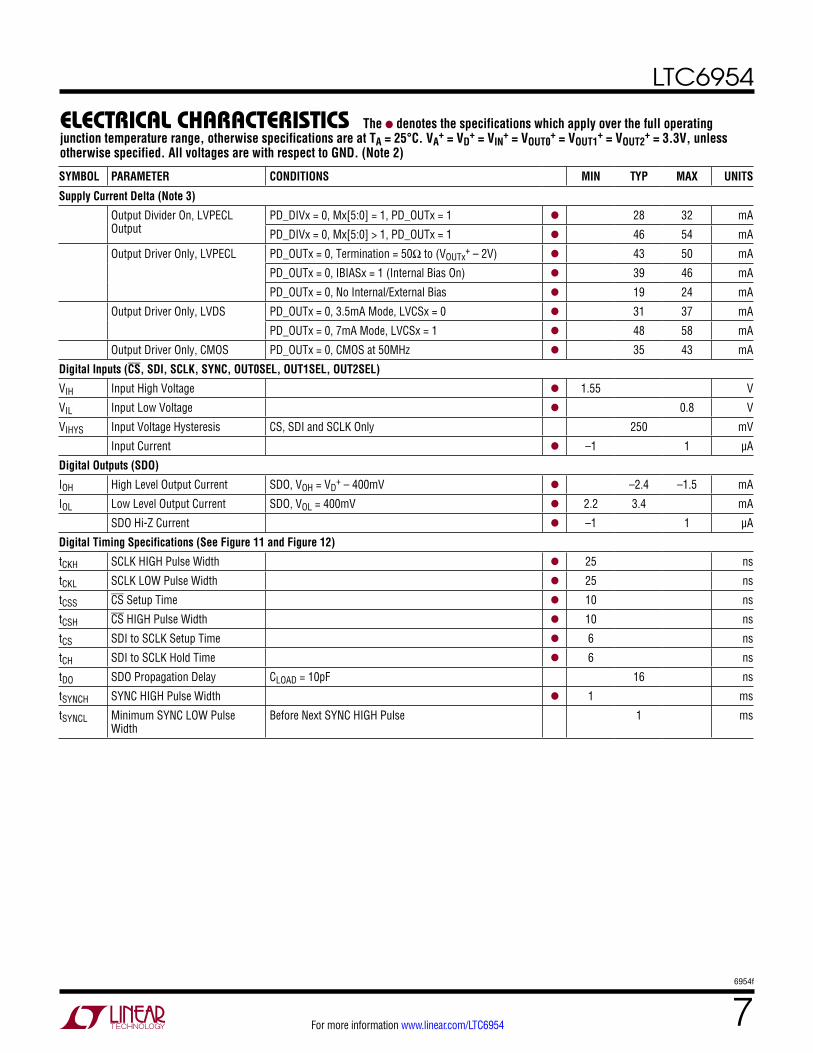
elecTrical characTerisTics The l denotes the specifications which apply over the full operating junction temperature range, otherwise specifications are at TA = 25°C. VA
+ = VD+ = VIN
+ = VOUT0+ = VOUT1
+ = VOUT2+ = 3.3V, unless
otherwise specified. All voltages are with respect to GND. (Note 2)
SYMBOL PARAMETER CONDITIONS MIN TYP MAX UNITS
Supply Current Delta (Note 3)
Output Divider On, LVPECL Output
PD_DIVx = 0, Mx[5:0] = 1, PD_OUTx = 1 l 28 32 mA
PD_DIVx = 0, Mx[5:0] > 1, PD_OUTx = 1 l 46 54 mA
Output Driver Only, LVPECL PD_OUTx = 0, Termination = 50Ω to (VOUTx+ – 2V) l 43 50 mA
PD_OUTx = 0, IBIASx = 1 (Internal Bias On) l 39 46 mA
PD_OUTx = 0, No Internal/External Bias l 19 24 mA
Output Driver Only, LVDS PD_OUTx = 0, 3.5mA Mode, LVCSx = 0 l 31 37 mA
PD_OUTx = 0, 7mA Mode, LVCSx = 1 l 48 58 mA
Output Driver Only, CMOS PD_OUTx = 0, CMOS at 50MHz l 35 43 mA
Digital Inputs (CS, SDI, SCLK, SYNC, OUT0SEL, OUT1SEL, OUT2SEL)
VIH Input High Voltage l 1.55 V
VIL Input Low Voltage l 0.8 V
VIHYS Input Voltage Hysteresis CS, SDI and SCLK Only 250 mV
Input Current l –1 1 µA
Digital Outputs (SDO)
IOH High Level Output Current SDO, VOH = VD+ – 400mV l –2.4 –1.5 mA
IOL Low Level Output Current SDO, VOL = 400mV l 2.2 3.4 mA
SDO Hi-Z Current l –1 1 µA
Digital Timing Specifications (See Figure 11 and Figure 12)
tCKH SCLK HIGH Pulse Width l 25 ns
tCKL SCLK LOW Pulse Width l 25 ns
tCSS CS Setup Time l 10 ns
tCSH CS HIGH Pulse Width l 10 ns
tCS SDI to SCLK Setup Time l 6 ns
tCH SDI to SCLK Hold Time l 6 ns
tDO SDO Propagation Delay CLOAD = 10pF 16 ns
tSYNCH SYNC HIGH Pulse Width l 1 ms
tSYNCL Minimum SYNC LOW Pulse Width
Before Next SYNC HIGH Pulse 1 ms
LTC6954
86954f
For more information www.linear.com/LTC6954
elecTrical characTerisTics The l denotes the specifications which apply over the full operating junction temperature range, otherwise specifications are at TA = 25°C. VA
+ = VD+ = VIN
+ = VOUT0+ = VOUT1
+ = VOUT2+ = 3.3V, unless
otherwise specified. All voltages are with respect to GND. (Note 2)
SYMBOL PARAMETER CONDITIONS MIN TYP MAX UNITS
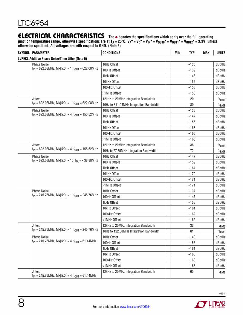
LVPECL Additive Phase Noise/Time Jitter (Note 5)
Phase Noise: fIN = 622.08MHz, Mx[5:0] = 1, fOUT = 622.08MHz
10Hz Offset –130 dBc/Hz
100Hz Offset –139 dBc/Hz
1kHz Offset –148 dBc/Hz
10kHz Offset –156 dBc/Hz
100kHz Offset –158 dBc/Hz
>1MHz Offset –158 dBc/Hz
Jitter: fIN = 622.08MHz, Mx[5:0] = 1, fOUT = 622.08MHz
12kHz to 20MHz Integration Bandwidth 20 fsRMS
10Hz to 311.04MHz Integration Bandwidth 80 fsRMS
Phase Noise: fIN = 622.08MHz, Mx[5:0] = 4, fOUT = 155.52MHz
10Hz Offset –138 dBc/Hz
100Hz Offset –147 dBc/Hz
1kHz Offset –156 dBc/Hz
10kHz Offset –163 dBc/Hz
100kHz Offset –165 dBc/Hz
>1MHz Offset –165 dBc/Hz
Jitter: fIN = 622.08MHz, Mx[5:0] = 4, fOUT = 155.52MHz
12kHz to 20MHz Integration Bandwidth 36 fsRMS
10Hz to 77.75MHz Integration Bandwidth 72 fsRMS
Phase Noise: fIN = 622.08MHz, Mx[5:0] = 16, fOUT = 38.88MHz
10Hz Offset –147 dBc/Hz
100Hz Offset –159 dBc/Hz
1kHz Offset –167 dBc/Hz
10kHz Offset –170 dBc/Hz
100kHz Offset –171 dBc/Hz
>1MHz Offset –171 dBc/Hz
Phase Noise: fIN = 245.76MHz, Mx[5:0] = 1, fOUT = 245.76MHz
10Hz Offset –137 dBc/Hz
100Hz Offset –147 dBc/Hz
1kHz Offset –156 dBc/Hz
10kHz Offset –161 dBc/Hz
100kHz Offset –162 dBc/Hz
>1MHz Offset –162 dBc/Hz
Jitter: fIN = 245.76MHz, Mx[5:0] = 1, fOUT = 245.76MHz
12kHz to 20MHz Integration Bandwidth 33 fsRMS
10Hz to 122.88MHz Integration Bandwidth 81 fsRMS
Phase Noise: fIN = 245.76MHz, Mx[5:0] = 4, fOUT = 61.44MHz
10Hz Offset –140 dBc/Hz
100Hz Offset –153 dBc/Hz
1kHz Offset –161 dBc/Hz
10kHz Offset –166 dBc/Hz
100kHz Offset –168 dBc/Hz
>1MHz Offset –168 dBc/Hz
Jitter: fIN = 245.76MHz, Mx[5:0] = 4, fOUT = 61.44MHz
12kHz to 20MHz Integration Bandwidth 65 fsRMS
LTC6954
96954f
For more information www.linear.com/LTC6954
elecTrical characTerisTics The l denotes the specifications which apply over the full operating junction temperature range, otherwise specifications are at TA = 25°C. VA
+ = VD+ = VIN
+ = VOUT0+ = VOUT1
+ = VOUT2+ = 3.3V, unless
otherwise specified. All voltages are with respect to GND. (Note 2)
SYMBOL PARAMETER CONDITIONS MIN TYP MAX UNITS
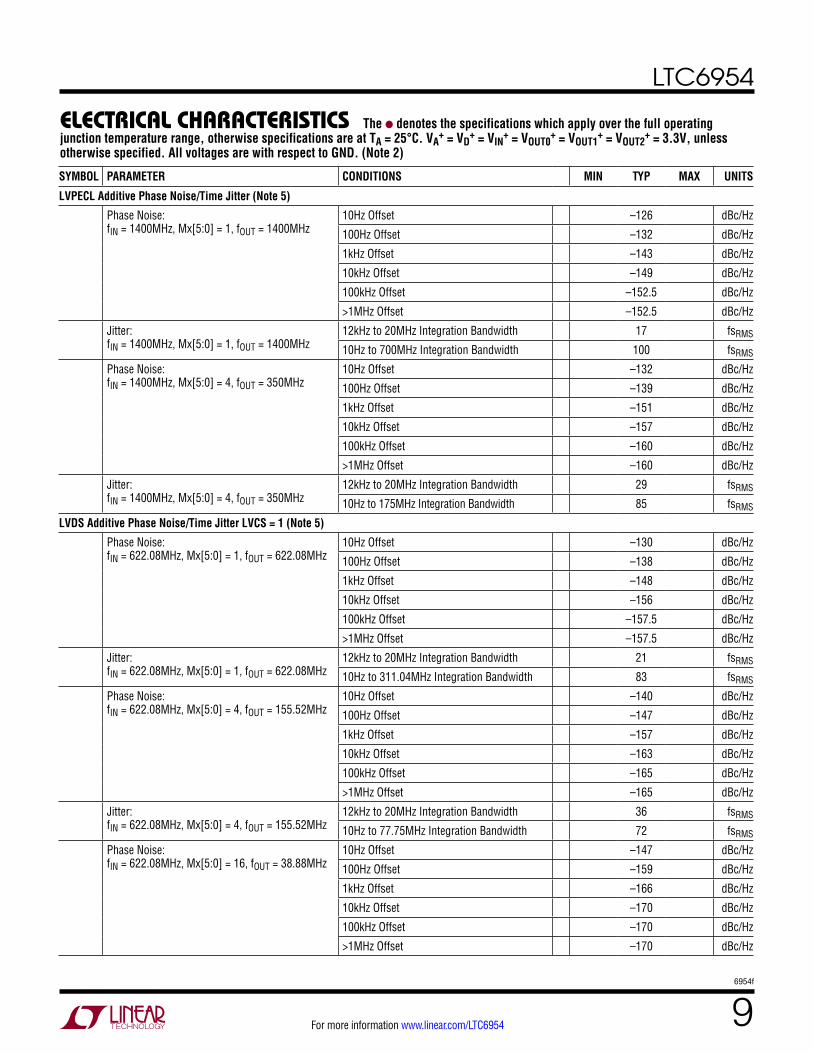
LVPECL Additive Phase Noise/Time Jitter (Note 5)
Phase Noise: fIN = 1400MHz, Mx[5:0] = 1, fOUT = 1400MHz
10Hz Offset –126 dBc/Hz
100Hz Offset –132 dBc/Hz
1kHz Offset –143 dBc/Hz
10kHz Offset –149 dBc/Hz
100kHz Offset –152.5 dBc/Hz
>1MHz Offset –152.5 dBc/Hz
Jitter: fIN = 1400MHz, Mx[5:0] = 1, fOUT = 1400MHz
12kHz to 20MHz Integration Bandwidth 17 fsRMS
10Hz to 700MHz Integration Bandwidth 100 fsRMS
Phase Noise: fIN = 1400MHz, Mx[5:0] = 4, fOUT = 350MHz
10Hz Offset –132 dBc/Hz
100Hz Offset –139 dBc/Hz
1kHz Offset –151 dBc/Hz
10kHz Offset –157 dBc/Hz
100kHz Offset –160 dBc/Hz
>1MHz Offset –160 dBc/Hz
Jitter: fIN = 1400MHz, Mx[5:0] = 4, fOUT = 350MHz
12kHz to 20MHz Integration Bandwidth 29 fsRMS
10Hz to 175MHz Integration Bandwidth 85 fsRMS
LVDS Additive Phase Noise/Time Jitter LVCS = 1 (Note 5)
Phase Noise: fIN = 622.08MHz, Mx[5:0] = 1, fOUT = 622.08MHz
10Hz Offset –130 dBc/Hz
100Hz Offset –138 dBc/Hz
1kHz Offset –148 dBc/Hz
10kHz Offset –156 dBc/Hz
100kHz Offset –157.5 dBc/Hz
>1MHz Offset –157.5 dBc/Hz
Jitter: fIN = 622.08MHz, Mx[5:0] = 1, fOUT = 622.08MHz
12kHz to 20MHz Integration Bandwidth 21 fsRMS
10Hz to 311.04MHz Integration Bandwidth 83 fsRMS
Phase Noise: fIN = 622.08MHz, Mx[5:0] = 4, fOUT = 155.52MHz
10Hz Offset –140 dBc/Hz
100Hz Offset –147 dBc/Hz
1kHz Offset –157 dBc/Hz
10kHz Offset –163 dBc/Hz
100kHz Offset –165 dBc/Hz
>1MHz Offset –165 dBc/Hz
Jitter: fIN = 622.08MHz, Mx[5:0] = 4, fOUT = 155.52MHz
12kHz to 20MHz Integration Bandwidth 36 fsRMS
10Hz to 77.75MHz Integration Bandwidth 72 fsRMS
Phase Noise: fIN = 622.08MHz, Mx[5:0] = 16, fOUT = 38.88MHz
10Hz Offset –147 dBc/Hz
100Hz Offset –159 dBc/Hz
1kHz Offset –166 dBc/Hz
10kHz Offset –170 dBc/Hz
100kHz Offset –170 dBc/Hz
>1MHz Offset –170 dBc/Hz
LTC6954
106954f
For more information www.linear.com/LTC6954
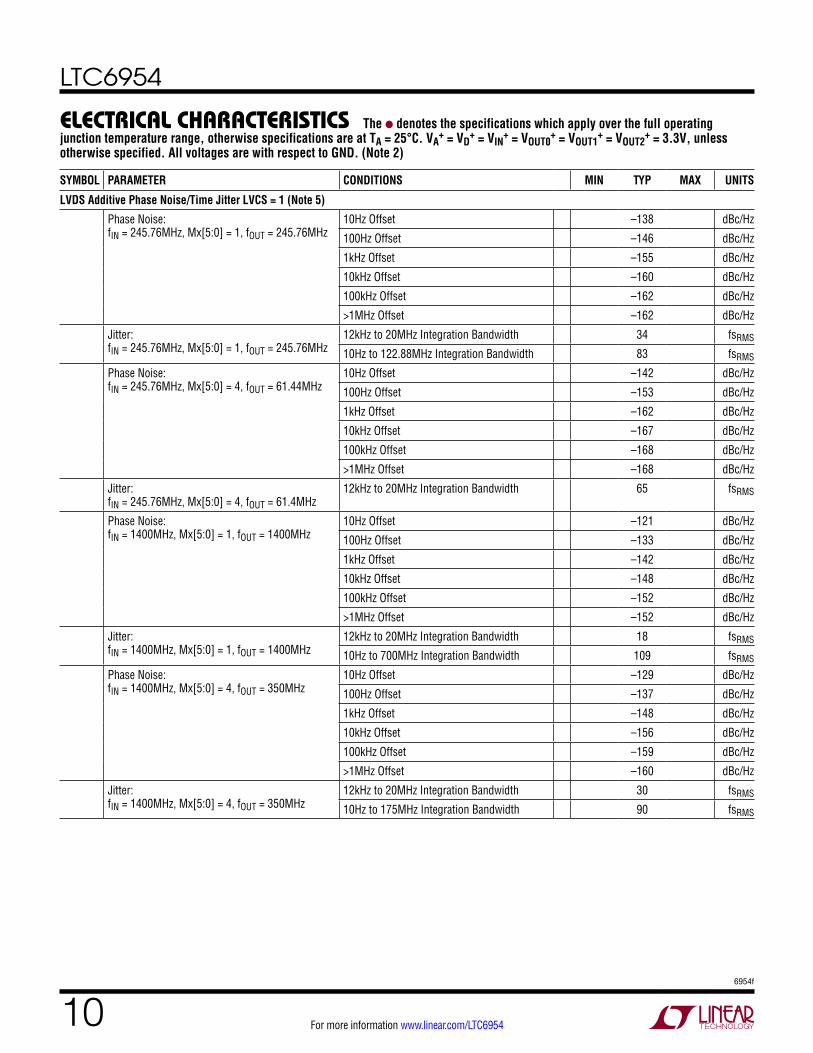
SYMBOL PARAMETER CONDITIONS MIN TYP MAX UNITS
LVDS Additive Phase Noise/Time Jitter LVCS = 1 (Note 5)
Phase Noise: fIN = 245.76MHz, Mx[5:0] = 1, fOUT = 245.76MHz
10Hz Offset –138 dBc/Hz
100Hz Offset –146 dBc/Hz
1kHz Offset –155 dBc/Hz
10kHz Offset –160 dBc/Hz
100kHz Offset –162 dBc/Hz
>1MHz Offset –162 dBc/Hz
Jitter: fIN = 245.76MHz, Mx[5:0] = 1, fOUT = 245.76MHz
12kHz to 20MHz Integration Bandwidth 34 fsRMS
10Hz to 122.88MHz Integration Bandwidth 83 fsRMS
Phase Noise: fIN = 245.76MHz, Mx[5:0] = 4, fOUT = 61.44MHz
10Hz Offset –142 dBc/Hz
100Hz Offset –153 dBc/Hz
1kHz Offset –162 dBc/Hz
10kHz Offset –167 dBc/Hz
100kHz Offset –168 dBc/Hz
>1MHz Offset –168 dBc/Hz
Jitter: fIN = 245.76MHz, Mx[5:0] = 4, fOUT = 61.4MHz
12kHz to 20MHz Integration Bandwidth 65 fsRMS
Phase Noise: fIN = 1400MHz, Mx[5:0] = 1, fOUT = 1400MHz
10Hz Offset –121 dBc/Hz
100Hz Offset –133 dBc/Hz
1kHz Offset –142 dBc/Hz
10kHz Offset –148 dBc/Hz
100kHz Offset –152 dBc/Hz
>1MHz Offset –152 dBc/Hz
Jitter: fIN = 1400MHz, Mx[5:0] = 1, fOUT = 1400MHz
12kHz to 20MHz Integration Bandwidth 18 fsRMS
10Hz to 700MHz Integration Bandwidth 109 fsRMS
Phase Noise: fIN = 1400MHz, Mx[5:0] = 4, fOUT = 350MHz
10Hz Offset –129 dBc/Hz
100Hz Offset –137 dBc/Hz
1kHz Offset –148 dBc/Hz
10kHz Offset –156 dBc/Hz
100kHz Offset –159 dBc/Hz
>1MHz Offset –160 dBc/Hz
Jitter: fIN = 1400MHz, Mx[5:0] = 4, fOUT = 350MHz
12kHz to 20MHz Integration Bandwidth 30 fsRMS
10Hz to 175MHz Integration Bandwidth 90 fsRMS
elecTrical characTerisTics The l denotes the specifications which apply over the full operating junction temperature range, otherwise specifications are at TA = 25°C. VA
+ = VD+ = VIN
+ = VOUT0+ = VOUT1
+ = VOUT2+ = 3.3V, unless
otherwise specified. All voltages are with respect to GND. (Note 2)
LTC6954
116954f
For more information www.linear.com/LTC6954
SYMBOL PARAMETER CONDITIONS MIN TYP MAX UNITS
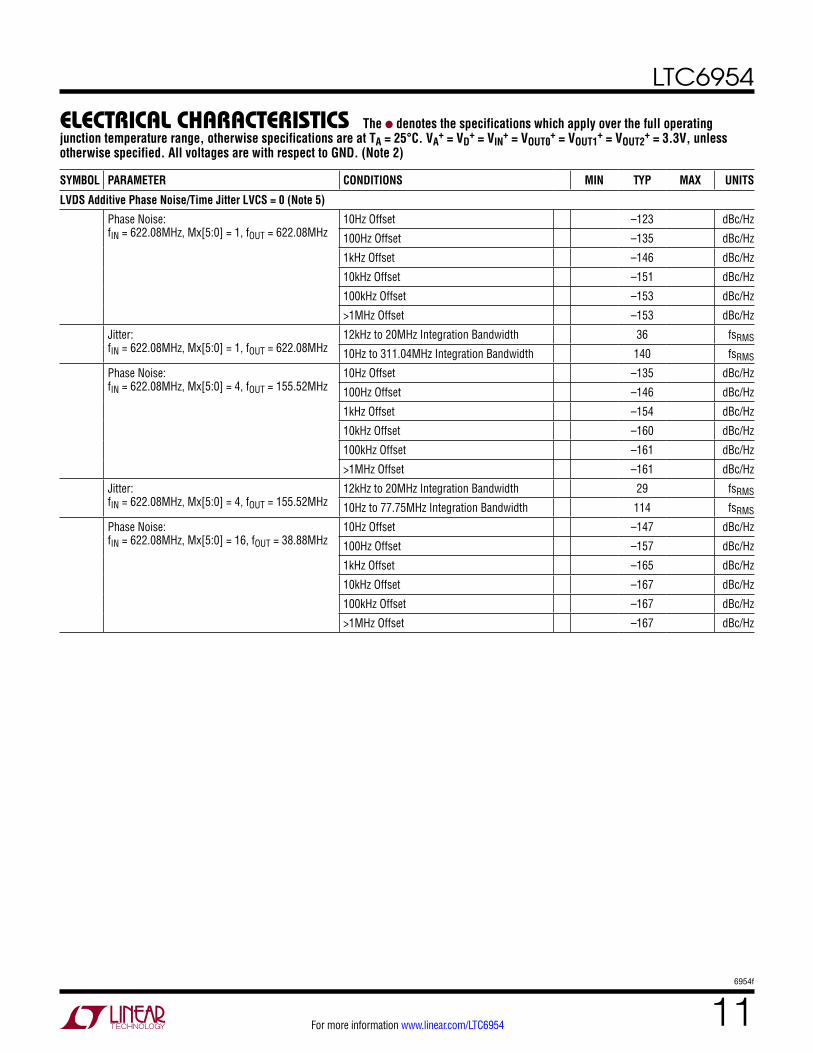
LVDS Additive Phase Noise/Time Jitter LVCS = 0 (Note 5)
Phase Noise: fIN = 622.08MHz, Mx[5:0] = 1, fOUT = 622.08MHz
10Hz Offset –123 dBc/Hz
100Hz Offset –135 dBc/Hz
1kHz Offset –146 dBc/Hz
10kHz Offset –151 dBc/Hz
100kHz Offset –153 dBc/Hz
>1MHz Offset –153 dBc/Hz
Jitter: fIN = 622.08MHz, Mx[5:0] = 1, fOUT = 622.08MHz
12kHz to 20MHz Integration Bandwidth 36 fsRMS
10Hz to 311.04MHz Integration Bandwidth 140 fsRMS
Phase Noise: fIN = 622.08MHz, Mx[5:0] = 4, fOUT = 155.52MHz
10Hz Offset –135 dBc/Hz
100Hz Offset –146 dBc/Hz
1kHz Offset –154 dBc/Hz
10kHz Offset –160 dBc/Hz
100kHz Offset –161 dBc/Hz
>1MHz Offset –161 dBc/Hz
Jitter: fIN = 622.08MHz, Mx[5:0] = 4, fOUT = 155.52MHz
12kHz to 20MHz Integration Bandwidth 29 fsRMS
10Hz to 77.75MHz Integration Bandwidth 114 fsRMS
Phase Noise: fIN = 622.08MHz, Mx[5:0] = 16, fOUT = 38.88MHz
10Hz Offset –147 dBc/Hz
100Hz Offset –157 dBc/Hz
1kHz Offset –165 dBc/Hz
10kHz Offset –167 dBc/Hz
100kHz Offset –167 dBc/Hz
>1MHz Offset –167 dBc/Hz
elecTrical characTerisTics The l denotes the specifications which apply over the full operating junction temperature range, otherwise specifications are at TA = 25°C. VA
+ = VD+ = VIN
+ = VOUT0+ = VOUT1
+ = VOUT2+ = 3.3V, unless
otherwise specified. All voltages are with respect to GND. (Note 2)
LTC6954
126954f
For more information www.linear.com/LTC6954
elecTrical characTerisTics The l denotes the specifications which apply over the full operating junction temperature range, otherwise specifications are at TA = 25°C. VA
+ = VD+ = VIN
+ = VOUT0+ = VOUT1
+ = VOUT2+ = 3.3V, unless
otherwise specified. All voltages are with respect to GND. (Note 2)
SYMBOL PARAMETER CONDITIONS MIN TYP MAX UNITS
CMOS Additive Phase Noise/Time Jitter (Note 5)
Phase Noise: fIN = 622.08MHz, Mx[5:0] = 4, fOUT = 155.52MHz
10Hz Offset –129 dBc/Hz
100Hz Offset –143 dBc/Hz
1kHz Offset –158 dBc/Hz
10kHz Offset –161 dBc/Hz
100kHz Offset –162 dBc/Hz
>1MHz Offset –162 dBc/Hz
Jitter: fIN = 622.08MHz, Mx[5:0] = 4, fOUT = 155.52MHz
12kHz to 20MHz Integration Bandwidth 52 fsRMS
10Hz to 77.75MHz Integration Bandwidth 102 fsRMS
Phase Noise: fIN = 245.76MHz, Mx[5:0] = 1, fOUT = 245.76MHz
10Hz Offset –129 dBc/Hz
100Hz Offset –139 dBc/Hz
1kHz Offset –146 dBc/Hz
10kHz Offset –155 dBc/Hz
100kHz Offset –159 dBc/Hz
>1MHz Offset –160 dBc/Hz
Jitter: fIN = 245.76MHz, Mx[5:0] = 1, fOUT = 245.76MHz
12kHz to 20MHz Integration Bandwidth 42 fsRMS
10Hz to 122.88MHz Integration Bandwidth 102 fsRMS
Phase Noise: fIN = 245.76MHz, Mx[5:0] = 4, fOUT = 61.44MHz
10Hz Offset –135 dBc/Hz
100Hz Offset –147 dBc/Hz
1kHz Offset –156 dBc/Hz
10kHz Offset –163 dBc/Hz
100kHz Offset –166 dBc/Hz
>1MHz Offset –166 dBc/Hz
Jitter: fIN = 245.76MHz, Mx[5:0] = 4, fOUT = 61.44MHz
12kHz to 20MHz Integration Bandwidth 82 fsRMS
Note 1: Stresses beyond those listed under Absolute Maximum Ratings may cause permanent damage to the device. Exposure to any Absolute Maximum Rating condition for extended periods may affect device reliability and lifetime.Note 2: The LTC6954I is guaranteed to meet specified performance limits over the full operating junction temperature range of –40°C to 105°C. Under maximum operating conditions, air flow or heat sinking may be required to maintain a junction temperature of 105°C or lower. It is strongly recommended that the exposed pad (pin 37) be soldered directly to the ground plane with an array of thermal vias as described in the Applications Information section. Note 3: The supply current delta specifications refer to the amount of supply current that each individual block consumes. Powering on or off this circuit block adds or subtracts this much current from the total supply current consumed in any given configuration.Note 4: The skews are defined as the second listed output's transition relative to the first listed output's transition. If the second listed output transitions after the first listed output, the skew is positive.
For the same divider setting, LVPECL outputs have nominally the same skew regardless of the IBIAS setting (IBIASx = 0 or 1), for the same divider setting, all LVDS and CMOS outputs transition after the LVPECL outputs, thus these skews are positive. For the same divider setting, all CMOS outputs transition after all LVDS outputs, thus these skews are positive. For the same divider setting, LVDS outputs with the 3.5mA current setting (LVCS = 0) transition after LVDS outputs with the 7mA current setting (LVCS = 1), thus these skews are positive. For the same divider setting, in-phase CMOS outputs (CMSINVx = 0) transition after complementary outputs (CMSINVx = 1), thus this skew is positive.For the same output type, outputs with the divider setting greater than one (Mx[5:0] > 1) transition after outputs with the divider equal to one (Mx[5:0] = 1), thus this additional skew is positive.Note 5: Additive phase noise and jitter are the phase noise added by the LTC6954. It does not include noise from the external signal source.
LTC6954
136954f
For more information www.linear.com/LTC6954
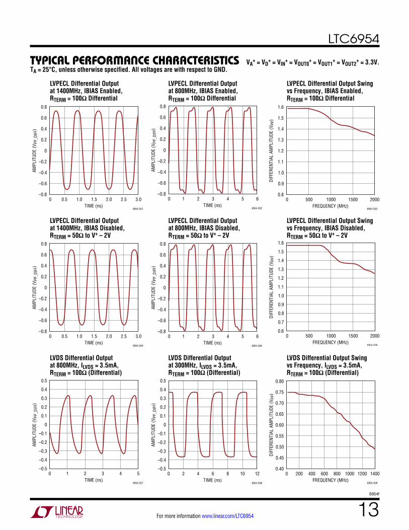
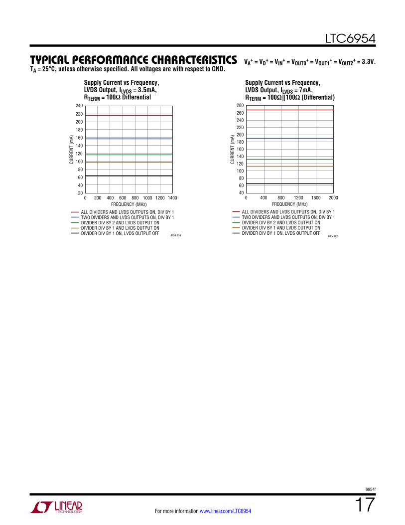
Typical perForMance characTerisTics
LVPECL Differential Output at 1400MHz, IBIAS Disabled, RTERM = 50Ω to V+ – 2V
LVPECL Differential Output at 800MHz, IBIAS Disabled, RTERM = 50Ω to V+ – 2V
LVPECL Differential Output Swing vs Frequency, IBIAS Disabled, RTERM = 50Ω to V+ – 2V
LVDS Differential Output at 800MHz, ILVDS = 3.5mA, RTERM = 100Ω (Differential)
LVDS Differential Output at 300MHz, ILVDS = 3.5mA, RTERM = 100Ω (Differential)
LVDS Differential Output Swing vs Frequency, ILVDS = 3.5mA, RTERM = 100Ω (Differential)
LVPECL Differential Output at 1400MHz, IBIAS Enabled, RTERM = 100Ω Differential
LVPECL Differential Output at 800MHz, IBIAS Enabled, RTERM = 100Ω Differential
LVPECL Differential Output Swing vs Frequency, IBIAS Enabled, RTERM = 100Ω Differential
VA+ = VD
+ = VIN+ = VOUT0
+ = VOUT1+ = VOUT2
+ = 3.3V. TA = 25°C, unless otherwise specified. All voltages are with respect to GND.
FREQUENCY (MHz)0
0.8
DIFF
EREN
TIAL
AM
PLIT
UDE
(VPP
)
1.0
1.2
1.4
500 1000 20001500
1.6
0.9
1.1
1.3
1.5
6954 G03
FREQUENCY (MHz)0
0.6
DIFF
EREN
TIAL
AM
PLIT
UDE
(VPP
)
0.9
1.2
1.4
500 1000 20001500
1.6
0.7
1.0
0.8
1.1
1.3
1.5
6954 G06
FREQUENCY (MHz)0
0.40
DIFF
EREN
TIAL
AM
PLIT
UDE
(VPP
)
0.50
0.60
0.70
400 800 14001200200 600 1000
0.80
0.45
0.55
0.65
0.75
6954 G09
TIME (ns)0
–0.8
AMPL
ITUD
E (V
PP_D
IFF)
–0.4
0
0.4
0.5 1.0 2.01.5 2.5
0.8
–0.6
–0.2
0.2
0.6
3.0
6954 G01TIME (ns)
0–0.8
AMPL
ITUD
E (V
PP_D
IFF)
–0.4
0
0.4
1 2 43 5
0.8
–0.6
–0.2
0.2
0.6
6
6954 G02
TIME (ns)0
–0.8
AMPL
ITUD
E (V
PP_D
IFF)
–0.4
0
0.4
0.5 1.0 2.01.5 2.5
0.8
–0.6
–0.2
0.2
0.6
3.0
6954 G04TIME (ns)
0–0.8
AMPL
ITUD
E (V
PP_D
IFF)
–0.4
0
0.4
1 2 43 5
0.8
–0.6
–0.2
0.2
0.6
6
6954 G05
TIME (ns)0
–0.5
AMPL
ITUD
E (V
PP_D
IFF)
–0.2
0
0.2
1 32 4
0.5
0.4
–0.3
–0.4
–0.1
0.1
0.3
5
6954 G07TIME (ns)
0–0.5
AMPL
ITUD
E (V
PP_D
IFF)
–0.2
0
0.2
2 64 8 10
0.5
0.4
–0.3
–0.4
–0.1
0.1
0.3
12
6954 G08

LTC6954
146954f
For more information www.linear.com/LTC6954
Typical perForMance characTerisTics
CMOS Output at 250MHz, CMSINV = 1, CLOAD = 2pF
CMOS Output at 100MHz, CMSINV = 1, CLOAD = 2pF
CMOS Output Swing vs Frequency and CLOAD
LVPECL Output Additive Phase Noise, fIN = 1400MHz, IBIAS Enabled,RTERM = 100Ω Differential
LVPECL Output Additive Phase Noise, fIN = 622.08MHz, IBIAS Enabled, RTERM = 100Ω Differential
LVPECL Output Additive Phase Noise, fIN = 245.76MHz, IBIAS Enabled, RTERM = 100Ω Differential
LVDS Differential Output at 1400MHz, ILVDS = 7mA, RTERM = 100Ω||100Ω (Differential)
LVDS Differential Output at 800MHz, ILVDS = 7mA, RTERM = 100Ω||100Ω (Differential)
LVDS Differential Output Swing vs Frequency, ILVDS = 7mA, RTERM = 100Ω||100Ω (Differential)
VA+ = VD
+ = VIN+ = VOUT0
+ = VOUT1+ = VOUT2
+ = 3.3V. TA = 25°C, unless otherwise specified. All voltages are with respect to GND.
TIME (ns)0
0
AMPL
ITUD
E (V
)
1.5
2.5
2 64 108 12 14
1.0
0.5
2.0
3.0
16
6954 G13TIME (ns)
00
AMPL
ITUD
E (V
)
1.5
2.5
5 1510 2520 30 35
1.0
0.5
2.0
3.0
40
6954 G14 FREQUENCY (MHz)0
2.0
V PP
SING
LE-E
NDED
(V)
2.6
3.0
50 150100 300200 350250 400 450
2.4
2.2
2.8
3.2
500
6954 G15
4.7pF
2pF
10pF
FREQUENCY (MHz)0
0.40
DIFF
EREN
TIAL
AM
PLIT
UDE
(VPP
)
0.50
0.60
0.70
1000 2000500 1500
0.80
0.45
0.55
0.65
0.75
6954 G12TIME (ns)
0–0.5
AMPL
ITUD
E (V
PP_D
IFF)
–0.2
0
0.2
0.25 0.75 1.751.250.50 1.0 2.01.50 2.25
0.5
0.4
–0.3
–0.4
–0.1
0.1
0.3
2.50
6954 G10
–180
ADDI
TIVE
PHA
SE N
OISE
(dBc
/Hz)
–150
–140
–120
–110
–160
–170
–130
6954 G16OFFSET FREQUENCY (Hz)
10 100 1k 1M 10M100k10k
SINGLE-ENDED SINE WAVE INPUT+7dBm AT 1.4GHz
DIV = 4
DIV = 16
–180
ADDI
TIVE
PHA
SE N
OISE
(dBc
/Hz)
–150
–140
–120
–160
–170
–130
6954 G17OFFSET FREQUENCY (Hz)
10 100 1k 1M 10M100k10k
DIV = 1
DIV = 4
DIV = 16
SINGLE-ENDED SINE WAVE INPUT+7dBm AT 622.08MHz
–180
ADDI
TIVE
PHA
SE N
OISE
(dBc
/Hz)
–150
–140
–160
–170
–130
6954 G18OFFSET FREQUENCY (Hz)
10 100 1k 1M 10M100k10k
DIV = 1
DIV = 4
SINGLE-ENDED SINE WAVE INPUT+7dBm AT 245.76MHz
TIME (ns)0
–0.8
AMPL
ITUD
E (V
PP_D
IFF)
–0.4
0
0.6
0.5 1.5 3.52.51 2 43 4.5
–0.6
–0.2
0.4
0.2
0.8
5
6954 G11
LTC6954
156954f
For more information www.linear.com/LTC6954
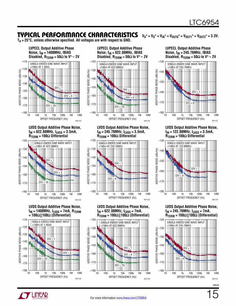
Typical perForMance characTerisTics
LVDS Output Additive Phase Noise, fIN = 622.08MHz, ILVDS = 3.5mA, RTERM = 100Ω Differential
LVDS Output Additive Phase Noise, fIN = 245.76MHz, ILVDS = 3.5mA, RTERM = 100Ω Differential
LVDS Output Additive Phase Noise, fIN = 122.88MHz, ILVDS = 3.5mA, RTERM = 100Ω Differential
LVDS Output Additive Phase Noise, fIN = 1400MHz, ILVDS = 7mA, RTERM = 100Ω||100Ω (Differential)
LVDS Output Additive Phase Noise, fIN = 622.08MHz, ILVDS = 7mA, RTERM = 100Ω||100Ω (Differential)
LVDS Output Additive Phase Noise, fIN = 245.76MHz, ILVDS = 7mA, RTERM = 100Ω||100Ω (Differential)
LVPECL Output Additive Phase Noise, fIN = 1400MHz, IBIAS Disabled, RTERM = 50Ω to V+ – 2V
LVPECL Output Additive Phase Noise, fIN = 622.08MHz, IBIAS Disabled, RTERM = 50Ω to V+ – 2V
LVPECL Output Additive Phase Noise, fIN = 245.76MHz, IBIAS Disabled, RTERM = 50Ω to V+ – 2V
VA+ = VD
+ = VIN+ = VOUT0
+ = VOUT1+ = VOUT2
+ = 3.3V. TA = 25°C, unless otherwise specified. All voltages are with respect to GND.
–180
ADDI
TIVE
PHA
SE N
OISE
(dBc
/Hz)
–150
–140
–160
–170
–110
–130
–120
6954 G19OFFSET FREQUENCY (Hz)
10 100 1k 1M 10M100k10k
DIV = 1
DIV = 4
DIV = 16
SINGLE-ENDED SINE WAVE INPUT+7dBm AT 1.4GHz
–180
ADDI
TIVE
PHA
SE N
OISE
(dBc
/Hz)
–150
–140
–160
–170
–130
–120
6954 G20OFFSET FREQUENCY (Hz)
10 100 1k 1M 10M100k10k
DIV = 1
DIV = 4
DIV = 16
SINGLE-ENDED SINE WAVE INPUT+7dBm AT 622.08MHz
–180
ADDI
TIVE
PHA
SE N
OISE
(dBc
/Hz)
–150
–140
–160
–170
–130
6954 G21OFFSET FREQUENCY (Hz)
10 100 1k 1M 10M100k10k
DIV = 1
DIV = 4
SINGLE-ENDED SINE WAVE INPUT+7dBm AT 245.76MHz
–180
ADDI
TIVE
PHA
SE N
OISE
(dBc
/Hz)
–150
–140
–160
–170
–110
–130
–120
6954 G25OFFSET FREQUENCY (Hz)
10 100 1k 1M 10M100k10k
DIV = 1
DIV = 16
DIV = 4
SINGLE-ENDED SINE WAVE INPUT+7dBm AT 1.4GHz
–180
ADDI
TIVE
PHA
SE N
OISE
(dBc
/Hz)
–150
–140
–160
–170
–130
–120
6954 G22OFFSET FREQUENCY (Hz)
10 100 1k 1M 10M100k10k
DIV = 1
DIV = 16
DIV = 4
SINGLE-ENDED SINE WAVE INPUT+7dBm AT 622.08MHz
–180
ADDI
TIVE
PHA
SE N
OISE
(dBc
/Hz)
–150
–140
–160
–170
–130
–120
6954 G23OFFSET FREQUENCY (Hz)
10 100 1k 1M 10M100k10k
DIV = 1
DIV = 4
SINGLE-ENDED SINE WAVE INPUT+7dBm AT 245.76MHz
–180
ADDI
TIVE
PHA
SE N
OISE
(dBc
/Hz)
–150
–140
–160
–170
–120
–130
6954 G26OFFSET FREQUENCY (Hz)
10 100 1k 1M 10M100k10k
DIV = 1
DIV = 4
DIV = 16
SINGLE-ENDED SINE WAVE INPUT+7dBm AT 622.08MHz
–180
ADDI
TIVE
PHA
SE N
OISE
(dBc
/Hz)
–150
–140
–160
–170
–120
–130
6954 G27OFFSET FREQUENCY (Hz)
10 100 1k 1M 10M100k10k
DIV = 1
DIV = 4
SINGLE-ENDED SINE WAVE INPUT+7dBm AT 245.76MHz
–180
ADDI
TIVE
PHA
SE N
OISE
(dBc
/Hz)
–150
–140
–160
–170
–130
6954 G24OFFSET FREQUENCY (Hz)
10 100 1k 1M 10M100k10k
DIV = 1
DIV = 4
SINGLE-ENDED SINE WAVE INPUT+7dBm AT 122.88MHz
LTC6954
166954f
For more information www.linear.com/LTC6954
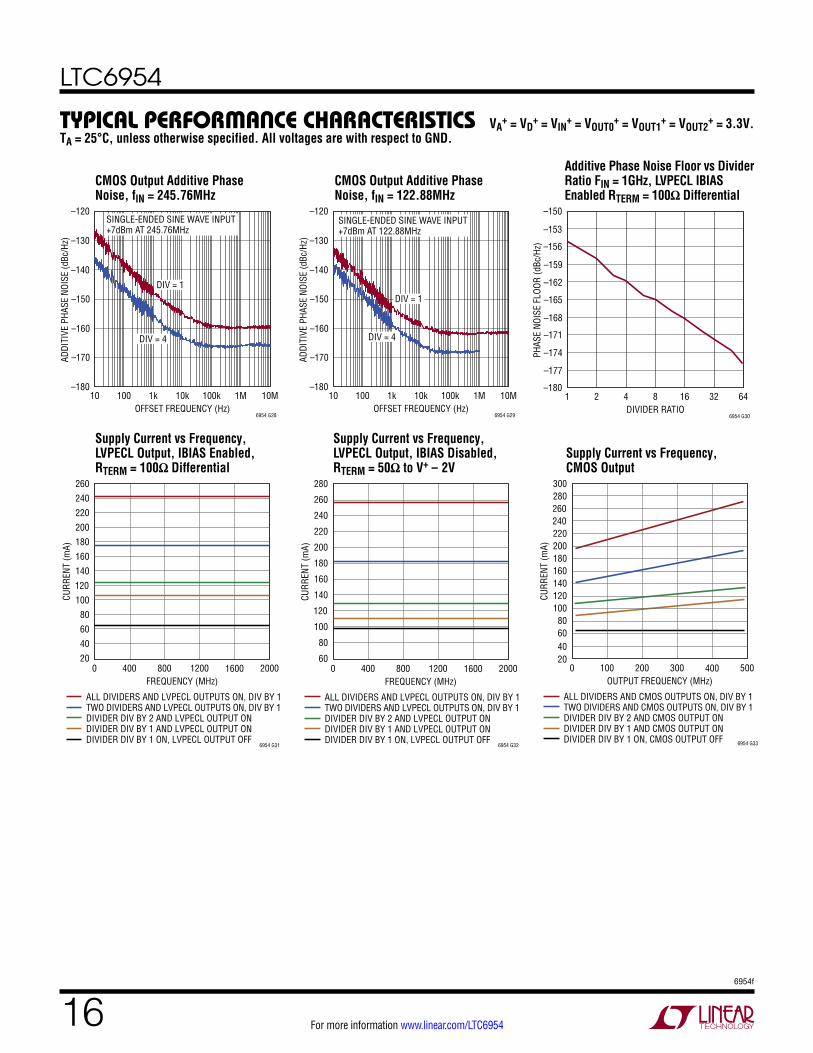
Typical perForMance characTerisTics
Supply Current vs Frequency, LVPECL Output, IBIAS Enabled, RTERM = 100Ω Differential
Supply Current vs Frequency, LVPECL Output, IBIAS Disabled, RTERM = 50Ω to V+ – 2V
Supply Current vs Frequency, CMOS Output
CMOS Output Additive Phase Noise, fIN = 245.76MHz
CMOS Output Additive Phase Noise, fIN = 122.88MHz
Additive Phase Noise Floor vs Divider Ratio FIN = 1GHz, LVPECL IBIAS Enabled RTERM = 100Ω Differential
VA+ = VD
+ = VIN+ = VOUT0
+ = VOUT1+ = VOUT2
+ = 3.3V. TA = 25°C, unless otherwise specified. All voltages are with respect to GND.
0 800 1600 2000400 1200FREQUENCY (MHz)
CURR
ENT
(mA)
100
200
220
240
260
60
160
80
180
40
20
140
120
6954 G31
ALL DIVIDERS AND LVPECL OUTPUTS ON, DIV BY 1TWO DIVIDERS AND LVPECL OUTPUTS ON, DIV BY 1DIVIDER DIV BY 2 AND LVPECL OUTPUT ONDIVIDER DIV BY 1 AND LVPECL OUTPUT ONDIVIDER DIV BY 1 ON, LVPECL OUTPUT OFF
0 800 1600 2000400 1200FREQUENCY (MHz)
CURR
ENT
(mA)
100
200
220
240
260
60
160
80
180
280
140
120
6954 G32
ALL DIVIDERS AND LVPECL OUTPUTS ON, DIV BY 1TWO DIVIDERS AND LVPECL OUTPUTS ON, DIV BY 1DIVIDER DIV BY 2 AND LVPECL OUTPUT ONDIVIDER DIV BY 1 AND LVPECL OUTPUT ONDIVIDER DIV BY 1 ON, LVPECL OUTPUT OFF
0 200 400 500100 300OUTPUT FREQUENCY (MHz)
CURR
ENT
(mA)
220
140
180
100
20
300
260
200
120
160
806040
280
240
6954 G33
ALL DIVIDERS AND CMOS OUTPUTS ON, DIV BY 1TWO DIVIDERS AND CMOS OUTPUTS ON, DIV BY 1DIVIDER DIV BY 2 AND CMOS OUTPUT ONDIVIDER DIV BY 1 AND CMOS OUTPUT ONDIVIDER DIV BY 1 ON, CMOS OUTPUT OFF
–180
ADDI
TIVE
PHA
SE N
OISE
(dBc
/Hz)
–150
–140
–160
–170
–130
–120
6954 G28OFFSET FREQUENCY (Hz)
10 100 1k 1M 10M100k10k
DIV = 1
DIV = 4
SINGLE-ENDED SINE WAVE INPUT+7dBm AT 245.76MHz
–180
ADDI
TIVE
PHA
SE N
OISE
(dBc
/Hz)
–150
–140
–160
–170
–130
–120
6954 G29OFFSET FREQUENCY (Hz)
10 100 1k 1M 10M100k10k
DIV = 1
DIV = 4
SINGLE-ENDED SINE WAVE INPUT+7dBm AT 122.88MHz
–180
PHAS
E NO
ISE
FLOO
R (d
Bc/H
z)
–159
–162
–165
–168
–171
–156
–174
–177
–153
–150
6954 G30DIVIDER RATIO
1 2 4 32 64168
LTC6954
176954f
For more information www.linear.com/LTC6954
0 800 1600 2000400 1200FREQUENCY (MHz)
CURR
ENT
(mA)
100
200
220
240
260
60
160
80
180
40
280
140
120
6954 G35
ALL DIVIDERS AND LVDS OUTPUTS ON, DIV BY 1TWO DIVIDERS AND LVDS OUTPUTS ON, DIV BY 1DIVIDER DIV BY 2 AND LVDS OUTPUT ONDIVIDER DIV BY 1 AND LVDS OUTPUT ONDIVIDER DIV BY 1 ON, LVDS OUTPUT OFF
VA+ = VD
+ = VIN+ = VOUT0
+ = VOUT1+ = VOUT2
+ = 3.3V. TA = 25°C, unless otherwise specified. All voltages are with respect to GND.
Supply Current vs Frequency, LVDS Output, ILVDS = 3.5mA, RTERM = 100Ω Differential
Supply Current vs Frequency, LVDS Output, ILVDS = 7mA, RTERM = 100Ω||100Ω (Differential)
Typical perForMance characTerisTics
0 400 1000 1400200 600 1200800FREQUENCY (MHz)
CURR
ENT
(mA)
100
200
220
240
60
160
80
20
40
180
140
120
6954 G34
ALL DIVIDERS AND LVDS OUTPUTS ON, DIV BY 1TWO DIVIDERS AND LVDS OUTPUTS ON, DIV BY 1DIVIDER DIV BY 2 AND LVDS OUTPUT ONDIVIDER DIV BY 1 AND LVDS OUTPUT ONDIVIDER DIV BY 1 ON, LVDS OUTPUT OFF
LTC6954
186954f
For more information www.linear.com/LTC6954
pin FuncTionsLTC6954
VOUT0+, VOUT1
+, VOUT2+ (Pins 1, 4, 5, 8, 9, 12): Output
Supply Voltages. The supply range is from 3.15V to 3.45V. This supply should be kept free of noise and ripple. The use of a low impedance power plane is recommended. All VOUTx
+ pins must be connected to the same supply volt-age as the VA
+, VD+ and VIN
+ pins. Each pin, or in some cases pin pairs, must be separately bypassed directly to GND with a 0.01µF ceramic capacitor as close to the pin as possible. Refer to the Applications Information section for more details on supply connections and bypassing.
GND (Pins 14, 26, 29, 32, 35): Ground Connections. Should be tied directly to the exposed pad (pin 37) and to a low impedance ground plane for best performance. Refer to the Applications Information section for more details on grounding for signal integrity and thermal considerations.
VA+ (Pins 15, 23, 24, 34): Analog Supply Voltages. The
supply range is from 3.15V to 3.45V. This supply should be kept free of noise and ripple. The use of a low imped-ance power plane is recommended. All VA
+ pins must be connected to the same supply voltage as the VOUTx
+, VD
+ and VIN+ pins. Each pin, or in some cases pin pairs,
must be separately bypassed directly to GND with a 0.1µF ceramic capacitor as close to the pin as possible. Refer to the Applications Information section for more details on supply connections and bypassing.
CS (Pin 16): Serial Port Chip Select Input. This active LOW CMOS logic input initiates a serial port transaction when brought LOW. It finalizes the serial port transaction when brought HIGH after 16 serial port clock cycles. Refer to the Operation section for more details.
SDO (Pin 17): Serial Data Output. Data read from the serial port is presented on this CMOS logic pin. Refer to the Operation section for more details.
VD+ (Pins 18, 21): Digital Supply Voltages. The supply
range is from 3.15V to 3.45V. This supply should be kept free of noise and ripple. The use of a low imped-ance power plane is recommended. All VD
+ pins must be connected to the same supply voltage as the VOUTx
+, VA
+ and VIN+ pins. Each pin must be separately bypassed
directly to GND with a 0.1µF ceramic capacitor as close to the pin as possible. Refer to the Applications Informa-
tion section for more details on supply connections and bypassing.
SCLK (Pin 19): Serial Port Clock Input. This positive edge triggered CMOS logic input signal clocks serial port data in on the rising edge. Refer to the Operation section for more details.
SDI (Pin 20): Serial Port Data Input. Data written into the serial port is presented on this CMOS logic pin. Refer to the Operation section for more details.
SYNC (Pin 22): The Synchronization Input Pin. A rising edge on this CMOS logic input initiates an output clock synchronization sequence. Precision output synchroniza-tion of one or more parts is handled on-chip, so the timing of this signal is not critical. Refer to the Operation and the Applications Information sections for more details.
VIN+ (Pins 25, 30): Analog Supply Voltages. The supply
range is from 3.15V to 3.45V. This supply should be kept free of noise and ripple. The use of a low impedance power plane is recommended. All VIN
+ pins must be connected to the same supply voltage as the VOUTx
+, VA+ and VD
+ pins. Each pin must be separately bypassed directly to GND with a 0.1µF ceramic capacitor as close to the pin as possible. Refer to the Applications Information section for more details on supply connections and bypassing.
IN+, IN– (Pins 27, 28): The Signal Input Pins. The input signal can be either differential or single ended. It can be a sine wave, LVPECL logic, LVDS logic or CMOS logic. Refer to the Operation and Applications Information sections for more details on the correct use of the inputs.
TEMP (Pin 31): Temperature Monitoring Diode. This pin is connected to the anode of a diode that may be used to measure the die temperature, by forcing a current and mea-suring the voltage. Refer to the Applications Information section for more details on monitoring the die temperature.
GND (Exposed Pad Pin 37): Ground Connection. The pack-age exposed pad must be soldered directly to the PCB land. The PCB land pattern should have multiple thermal vias to the ground plane for both low ground inductance and low thermal resistance. Refer to the Applications Information section for more details on grounding for signal integrity and thermal considerations.
LTC6954
196954f
For more information www.linear.com/LTC6954
pin FuncTionsLTC6954-1 OUTPUTS AND MODE SELECT
OUT0SEL (Pin 13): OUT0 Mode Select. Connecting this pin to the VA
+ supply enables the internal, active biasing of the OUT0 output emitter followers. Connecting this pin to GND disables this internal bias circuit. Refer to the Operation and Applications Information sections for more details on the LVPECL internal bias.
OUT0–, OUT0+ (Pins 10, 11): LVPECL Output Pins. Differential logic outputs typically terminated by 50Ω con-nected to a supply 2V below the VOUT0
+ supply. Refer to the Operation and Applications Information sections for more details.
OUT1SEL (Pin 33): OUT1 Mode Select. Connecting this pin to the VA
+ supply enables the internal, active biasing of the OUT1 output emitter followers. Connecting this pin to GND disables this internal bias circuit. Refer to the Operation and Applications Information sections for more details on the LVPECL internal bias.
OUT1–, OUT1+ (Pins 6, 7): LVPECL Output Pins. Differential logic outputs typically terminated by 50Ω connected to a supply 2V below the VOUT1
+ supply. Refer to the Operation and Applications Information sections for more details.
OUT2SEL (Pin 36): OUT2 Mode Select. Connecting this pin to the VA
+ supply enables the internal, active biasing of the OUT2 output emitter followers. Connecting this pin to GND disables this internal bias circuit. Refer to the Operation and Applications Information sections for more details on the LVPECL internal bias.
OUT2–, OUT2+ (Pins 2, 3): LVPECL Output Pins. Differential logic outputs typically terminated by 50Ω connected to a supply 2V below the VOUT2
+ supply. Refer to the Operation and Applications Information sections for more details.
LTC6954-2 OUTPUTS AND MODE SELECT
OUT0SEL (Pin 13): OUT0 Mode Select. Connecting this pin to the VA
+ supply enables the internal, active biasing of the OUT0 output emitter followers. Connecting this pin to GND disables this internal bias circuit. Refer to the Operation and Applications Information sections for more details on the LVPECL internal bias.
OUT0–, OUT0+ (Pins 10, 11): LVPECL Output Pins. Dif-ferential logic outputs typically terminated by 50Ω con-nected to a supply 2V below the VOUT0
+ supply. Refer to the Operation and Applications Information sections for more details.
OUT1SEL (Pin 33): OUT1 Mode Select. Connecting this pin to the VA
+ supply enables the internal, active biasing of the OUT1 output emitter followers. Connecting this pin to GND disables this internal bias circuit. Refer to the Operation and Applications Information sections for more details on the LVPECL internal bias.
OUT1–, OUT1+ (Pins 6, 7): LVPECL Output Pins. Differential logic outputs typically terminated by 50Ω connected to a supply 2V below the VOUT1
+ supply. Refer to the Operation and Applications Information sections for more details.
OUT2SEL (Pin 36): OUT2 Mode Select. Connecting this pin to ground configures OUT2 as a CMOS logic type output. Connecting this pin to the VA
+ supply configures OUT2 as an LVDS logic type output.
OUT2–, OUT2+ (Pins 2, 3): LVDS/CMOS Output Pins. These outputs may be programmed as LVDS or CMOS outputs using the OUT2SEL pin. Refer to the Op-eration and the Applications Information sections for more details.
LTC6954
206954f
For more information www.linear.com/LTC6954
pin FuncTionsLTC6954-3 OUTPUTS AND MODE SELECT
OUT0SEL (Pin 13): OUT0 Mode Select. Connecting this pin to the VA
+ supply enables the internal, active biasing of the OUT0 output emitter followers. Connecting this pin to GND disables this internal bias circuit. Refer to the Operation and Applications Information sections for more details on the LVPECL internal bias.
OUT0–, OUT0+ (Pins 10, 11): LVPECL Output Pins. Dif-ferential logic outputs typically terminated by 50Ω con-nected to a supply 2V below the VOUT0
+ supply. Refer to the Operation and Applications Information sections for more details.
OUT1SEL (Pin 33): OUT1 Mode Select. Connecting this pin to GND configures OUT1 as a CMOS logic type output. Connecting this pin to the VA
+ supply configures OUT1 as an LVDS logic type output.
OUT1–, OUT1+ (Pins 6, 7): LVDS/CMOS Output Pins. These outputs may be programmed as LVDS or CMOS outputs using the OUT1SEL pin. Refer to the Operation and the Applications Information sections for more details.
OUT2SEL (Pin 36): OUT2 Mode Select. Connecting this pin to GND configures OUT2 as a CMOS logic type output. Connecting this pin to the VA
+ supply configures OUT2 as an LVDS logic type output.
OUT2–, OUT2+ (Pins 2, 3): LVDS/CMOS Output Pins. These outputs may be programmed as LVDS or CMOS outputs using the OUT2SEL pin. Refer to the Operation and the Applications Information sections for more details.
LTC6954-4 OUTPUTS AND MODE SELECT
OUT0SEL (Pin 13): OUT0 Mode Select. Connecting this pin to GND configures OUT0 as a CMOS logic type output. Connecting this pin to the VA
+ supply configures OUT0 as an LVDS logic type output.
OUT0–, OUT0+ (Pins 10, 11): LVDS/CMOS Output Pins. These outputs may be programmed as LVDS or CMOS outputs using the OUT0SEL pin. Refer to the Operation and the Applications Information sections for more details.
OUT1SEL (Pin 33): OUT1 Mode Select. Connecting this pin to GND configures OUT1 as a CMOS logic type output. Connecting this pin to the VA
+ supply configures OUT1 as an LVDS logic type output.
OUT1–, OUT1+ (Pins 6, 7): LVDS/CMOS Output Pins. These outputs may be programmed as LVDS or CMOS outputs using the OUT1SEL pin. Refer to the Operation and the Applications Information sections for more details.
OUT2SEL (Pin 36): OUT2 Mode Select. Connecting this pin to GND configures OUT2 as a CMOS logic type output. Connecting this pin to the VA
+ supply configures OUT2 as an LVDS logic type output.
OUT2–, OUT2+ (Pins 2, 3): LVDS/CMOS Output Pins. These outputs may be programmed as LVDS or CMOS outputs using the OUT2SEL pin. Refer to the Operation and the Applications Information sections for more details.
LTC6954
216954f
For more information www.linear.com/LTC6954
block DiagraM
6954 BD
OUT0+
OUT0–M0 DIVIDERM0 = 1 TO 63
OUTPUT 0DRIVER
DELAY 0DEL0 = 0 TO 63
SDI
CS
SDO
SCLK
VD+
VD+18
17
19
20
16
SYNC SYNCCONTROL
SPISERIALPORTAND
DIGITALLOGIC
EXPOSEDGND PAD
IN+
IN–
26
27
28
GND
VIN+
GND
32GND
14GND
35GND
37
25
GND
VIN+
TEMP
30
31
29
VOUT0+
VOUT0+
9
11
10
12
OUT1+
OUT1–M1 DIVIDERM1 = 1 TO 63
OUTPUT 1DRIVER
DELAY 1DEL1 = 0 TO 63
VOUT1+
VOUT1+
5
7
6
8
OUT2+
OUT2–M2 DIVIDERM2 = 1 TO 63
OUTPUT 2DRIVER
DELAY 2DEL2 = 0 TO 63
VOUT2+
VOUT2+
1
3
2
4
15
VA+
23
VA+
24
VA+
34
VA+
OUT1SEL
OUT2SEL
OUT0SEL13
33
36
21
22
LTC6954
226954f
For more information www.linear.com/LTC6954
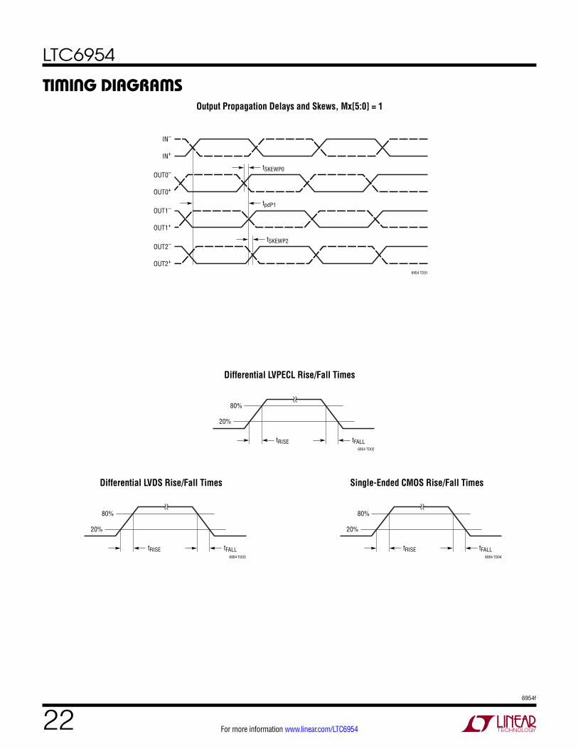
TiMing DiagraMs
IN–
IN+
OUT0–
OUT0+
OUT2–
OUT2+
OUT1–
OUT1+
6954 TD01
tSKEWP2
tSKEWP0
tpdP1
Output Propagation Delays and Skews, Mx[5:0] = 1
Differential LVPECL Rise/Fall Times
Differential LVDS Rise/Fall Times Single-Ended CMOS Rise/Fall Times
6954 TD02
tFALL
80%
20%
tRISE
6954 TD03
tFALL
80%
20%
tRISE6954 TD04
tFALL
80%
20%
tRISE
LTC6954
236954f
For more information www.linear.com/LTC6954
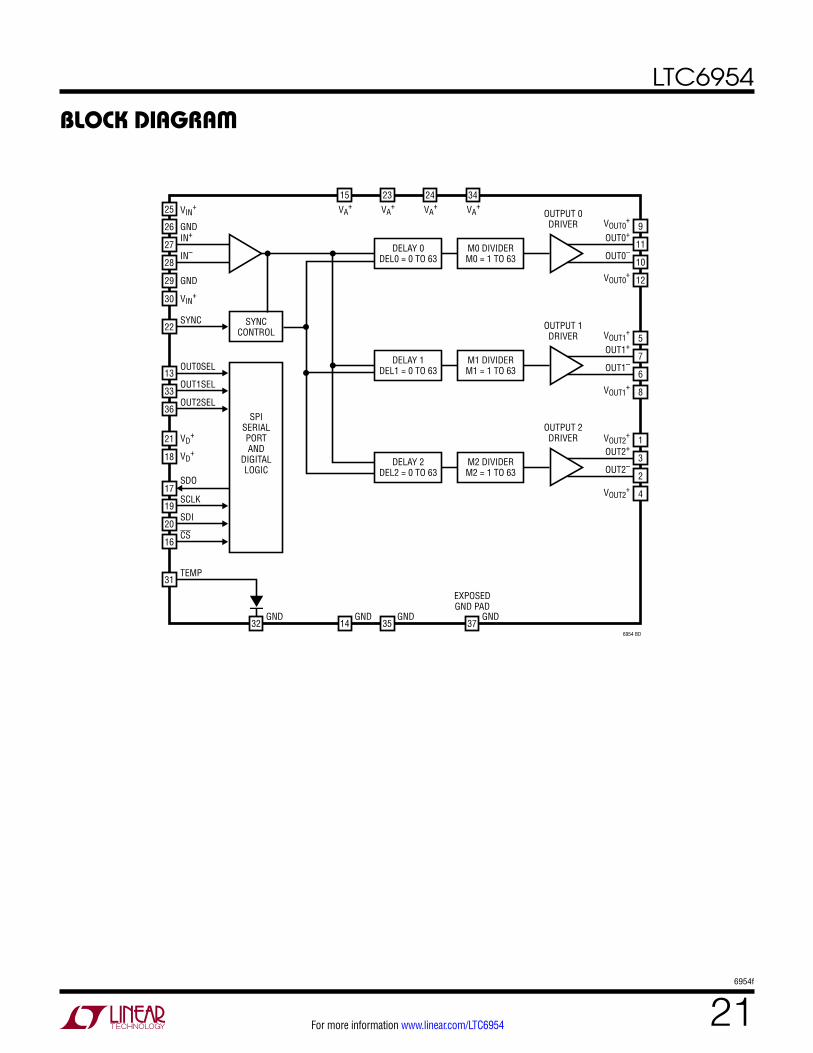
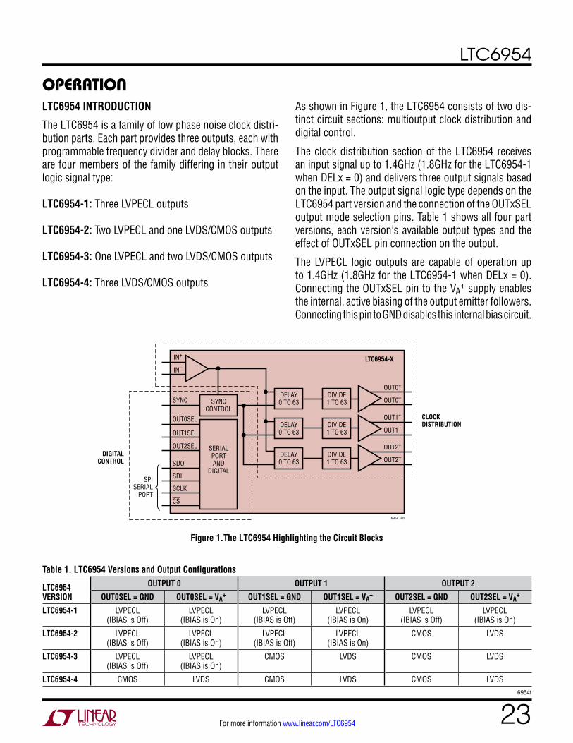
operaTionLTC6954 INTRODUCTION
The LTC6954 is a family of low phase noise clock distri-bution parts. Each part provides three outputs, each with programmable frequency divider and delay blocks. There are four members of the family differing in their output logic signal type:
LTC6954-1: Three LVPECL outputs
LTC6954-2: Two LVPECL and one LVDS/CMOS outputs
LTC6954-3: One LVPECL and two LVDS/CMOS outputs
LTC6954-4: Three LVDS/CMOS outputs
As shown in Figure 1, the LTC6954 consists of two dis-tinct circuit sections: multioutput clock distribution and digital control.
The clock distribution section of the LTC6954 receives an input signal up to 1.4GHz (1.8GHz for the LTC6954-1 when DELx = 0) and delivers three output signals based on the input. The output signal logic type depends on the LTC6954 part version and the connection of the OUTxSEL output mode selection pins. Table 1 shows all four part versions, each version’s available output types and the effect of OUTxSEL pin connection on the output.
The LVPECL logic outputs are capable of operation up to 1.4GHz (1.8GHz for the LTC6954-1 when DELx = 0). Connecting the OUTxSEL pin to the VA
+ supply enables the internal, active biasing of the output emitter followers. Connecting this pin to GND disables this internal bias circuit.
Figure 1.The LTC6954 Highlighting the Circuit Blocks
Table 1. LTC6954 Versions and Output Configurations
LTC6954 VERSION
OUTPUT 0 OUTPUT 1 OUTPUT 2
OUT0SEL = GND OUT0SEL = VA+ OUT1SEL = GND OUT1SEL = VA
+ OUT2SEL = GND OUT2SEL = VA+
LTC6954-1 LVPECL (IBIAS is Off)
LVPECL (IBIAS is On)
LVPECL (IBIAS is Off)
LVPECL (IBIAS is On)
LVPECL (IBIAS is Off)
LVPECL (IBIAS is On)
LTC6954-2 LVPECL (IBIAS is Off)
LVPECL (IBIAS is On)
LVPECL (IBIAS is Off)
LVPECL (IBIAS is On)
CMOS LVDS
LTC6954-3 LVPECL (IBIAS is Off)
LVPECL (IBIAS is On)
CMOS LVDS CMOS LVDS
LTC6954-4 CMOS LVDS CMOS LVDS CMOS LVDS
6954 F01
CLOCKDISTRIBUTION
OUT2+
OUT2–DIVIDE1 TO 63
DELAY0 TO 63
OUT1+
OUT1–DIVIDE1 TO 63
DELAY0 TO 63
OUT0+
OUT0–
SPISERIAL
PORT
DIVIDE1 TO 63
DELAY0 TO 63
DIGITALCONTROL
SCLK
CS
SDO
SDI
OUT0SEL
OUT1SEL
OUT2SEL
SYNC
IN+
IN–LTC6954-X
SYNCCONTROL
SERIALPORTAND
DIGITAL
LTC6954
246954f
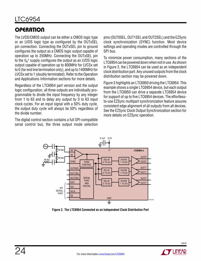
For more information www.linear.com/LTC6954
operaTionThe LVDS/CMOS output can be either a CMOS logic type or an LVDS logic type as configured by the OUTxSEL pin connection. Connecting the OUTxSEL pin to ground configures the output as a CMOS logic output capable of operation up to 250MHz. Connecting the OUTxSEL pin to the VA
+ supply configures the output as an LVDS logic output capable of operation up to 800MHz for LVCSx set to 0 (far end line termination only), and up to 1400MHz for LVCSx set to 1 (doubly terminated). Refer to the Operation and Applications Information sections for more details.
Regardless of the LTC6954 part version and the output logic configuration, all three outputs are individually pro-grammable to divide the input frequency by any integer from 1 to 63 and to delay any output by 0 to 63 input clock cycles. For an input signal with a 50% duty cycle, the output duty cycle will always be 50% regardless of the divide number.
The digital control section contains a full SPI-compatible serial control bus, the three output mode selection
pins (OUT0SEL, OUT1SEL and OUT2SEL) and the EZSync clock synchronization (SYNC) function. Most device settings and operating modes are controlled through the SPI bus.
To minimize power consumption, many sections of the LTC6954 can be powered down when not in use. As shown in Figure 2, the LTC6954 can be used as an independent clock distribution part. Any unused outputs from the clock distribution section may be powered down.
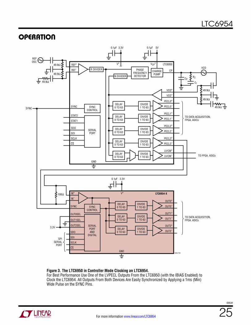
Figure 3 highlights an LTC6950 driving the LTC6954. This example shows a single LTC6954 device, but each output from the LTC6950 can drive a separate LTC6954 device for support of up to five LTC6954 devices. The effortless-to-use EZSync multipart synchronization feature assures consistent edge alignment of all outputs from all devices. See the EZSync Clock Output Synchronization section for more details on EZSync operation.
Figure 2. The LTC6954 Connected as an Independent Clock Distribution Part
6954 F02
OUT2+
OUT2–DIVIDE1 TO 63
DELAY0 TO 63
OUT1+
OUT1–DIVIDE1 TO 63
DELAY0 TO 63
OUT0+
OUT0–
SPISERIAL
PORT
DIVIDE1 TO 63
DELAY0 TO 63
V+
3.3V0.1µF
SCLK
CSGND
SDO
SDI
OUT0SEL
OUT1SEL
OUT2SEL
SYNC
IN+
IN–
LTC6954-x49.9Ω
49.9Ω49.9Ω
SYNCCONTROL
SERIALPORTAND
DIGITAL
LTC6954
256954f
For more information www.linear.com/LTC6954
operaTion
Figure 3. The LTC6950 in Controller Mode Clocking an LTC6954. For Best Performance Use One of the LVPECL Outputs From the LTC6950 (with the IBIAS Enabled) to Clock the LTC6954. All Outputs From Both Devices Are Easily Synchronized by Applying a 1ms (Min) Wide Pulse on the SYNC Pins.
LV/CM+
TO DATA ACQUISITION,FPGA, ASICs
TO DATA ACQUISITION,FPGA, ASICs
TO FPGA, ASICsLV/CM–DIVIDE1 TO 63
DELAY0 TO 63
PECL3+
PECL3–DIVIDE1 TO 63
DELAY0 TO 63
PECL2+
PECL2–DIVIDE1 TO 63
DELAY0 TO 63
PECL1+
PECL1–DIVIDE1 TO 63
DELAY0 TO 63
PECL0+
PECL0–
RZ
CI
VCO
REFOSC
49.9Ω
49.9Ω
49.9Ω
49.9Ω
0.1µF 5V
49.9Ω
49.9ΩCP
DIVIDE1 TO 63
DELAY0 TO 63
VCO+
VCP+V+
VCO–
SCLK
CS
SDO
SDI
STAT2
STAT1
SYNCSYNC SYNC
CONTROL
SERIALPORT
CHARGEPUMP
PHASEFREQUENCYDETECTORN DIVIDER
R DIVIDER
REF+
REF–
LTC6950
CP
6954 F03
OUT2+
OUT2–DIVIDE1 TO 63
DELAY0 TO 63
OUT1+
OUT1–DIVIDE1 TO 63
DELAY0 TO 63
OUT0+
OUT0–
SPISERIAL
PORT
DIVIDE1 TO 63
DELAY0 TO 63
V+
3.3V0.1µF
GND
3.3V
SCLK
CSGND
SDO
SDI
OUT0SEL
OUT1SEL
OUT2SEL
SYNC
IN+
IN–
LTC6954-X
SYNCCONTROL
SERIALPORTAND
DIGITAL
100Ω
0.1µF 3.3V
LTC6954
266954f
For more information www.linear.com/LTC6954
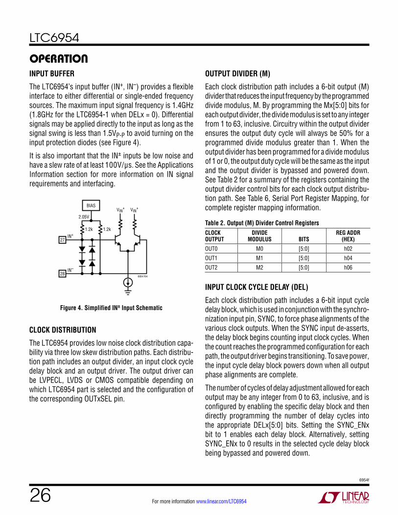
operaTionINPUT BUFFER
The LTC6954’s input buffer (IN+, IN–) provides a flexible interface to either differential or single-ended frequency sources. The maximum input signal frequency is 1.4GHz (1.8GHz for the LTC6954-1 when DELx = 0). Differential signals may be applied directly to the input as long as the signal swing is less than 1.5VP-P to avoid turning on the input protection diodes (see Figure 4).
It is also important that the IN± inputs be low noise and have a slew rate of at least 100V/µs. See the Applications Information section for more information on IN signal requirements and interfacing.
Figure 4. Simplified IN± Input Schematic
OUTPUT DIVIDER (M)
Each clock distribution path includes a 6-bit output (M) divider that reduces the input frequency by the programmed divide modulus, M. By programming the Mx[5:0] bits for each output divider, the divide modulus is set to any integer from 1 to 63, inclusive. Circuitry within the output divider ensures the output duty cycle will always be 50% for a programmed divide modulus greater than 1. When the output divider has been programmed for a divide modulus of 1 or 0, the output duty cycle will be the same as the input and the output divider is bypassed and powered down. See Table 2 for a summary of the registers containing the output divider control bits for each clock output distribu-tion path. See Table 6, Serial Port Register Mapping, for complete register mapping information.
Table 2. Output (M) Divider Control Registers CLOCK OUTPUT
DIVIDE MODULUS BITS
REG ADDR (HEX)
OUT0 M0 [5:0] h02
OUT1 M1 [5:0] h04
OUT2 M2 [5:0] h06
INPUT CLOCK CYCLE DELAY (DEL)
Each clock distribution path includes a 6-bit input cycle delay block, which is used in conjunction with the synchro-nization input pin, SYNC, to force phase alignments of the various clock outputs. When the SYNC input de-asserts, the delay block begins counting input clock cycles. When the count reaches the programmed configuration for each path, the output driver begins transitioning. To save power, the input cycle delay block powers down when all output phase alignments are complete.
The number of cycles of delay adjustment allowed for each output may be any integer from 0 to 63, inclusive, and is configured by enabling the specific delay block and then directly programming the number of delay cycles into the appropriate DELx[5:0] bits. Setting the SYNC_ENx bit to 1 enables each delay block. Alternatively, setting SYNC_ENx to 0 results in the selected cycle delay block being bypassed and powered down.
CLOCK DISTRIBUTION
The LTC6954 provides low noise clock distribution capa-bility via three low skew distribution paths. Each distribu-tion path includes an output divider, an input clock cycle delay block and an output driver. The output driver can be LVPECL, LVDS or CMOS compatible depending on which LTC6954 part is selected and the configuration of the corresponding OUTxSEL pin.
27
28
1.2kIN+
IN–
1.2k
6954 F04
2.05V
BIASVIN
+ VIN+
LTC6954
276954f
For more information www.linear.com/LTC6954
operaTionBecause the input clock cycle delay block operates inde-pendently of the output divider block, the programmed cycle delay adjustment occurs regardless of the modulus setting of the output divider (see the example in Figure 5).
Refer to the EZSync Clock Output Synchronization section for more information about using the SYNC input pin to achieve specific output phase alignments.
See Table 3 for a summary of the registers contain-ing the output delay control bits for each clock output distribution path. For complete register mapping in-formation, see Table 6, Serial Port Register Mapping.
Table 3. Output Delay (DEL) Control Registers CLOCK OUTPUT
OUTPUT DELAY BITS
SYNC ENABLE BIT
REG ADDR (HEX)
OUT0 DEL0 [5:0] SYNC_EN0 [7] h01
OUT1 DEL1 [5:0] SYNC_EN1 [7] h03
OUT2 DEL2 [5:0] SYNC_EN2 [7] h05
Figure 5. Input Clock Delay Operation (M0 = M1 = M2 = 4, DEL0 = 0, DEL1 = 1, DEL2 = 11)
IN
6954 F05
OUT0
OUT1
OUT2
1 INPUT CYCLE DELAY
1 INPUT CYCLE
0 1 2 3 4 5 6 7 8 9 10 11
11 INPUT CYCLE DELAY
SYNC DE-ASSERTED EARLIER
LVDS/CMOS OUTPUT DRIVER
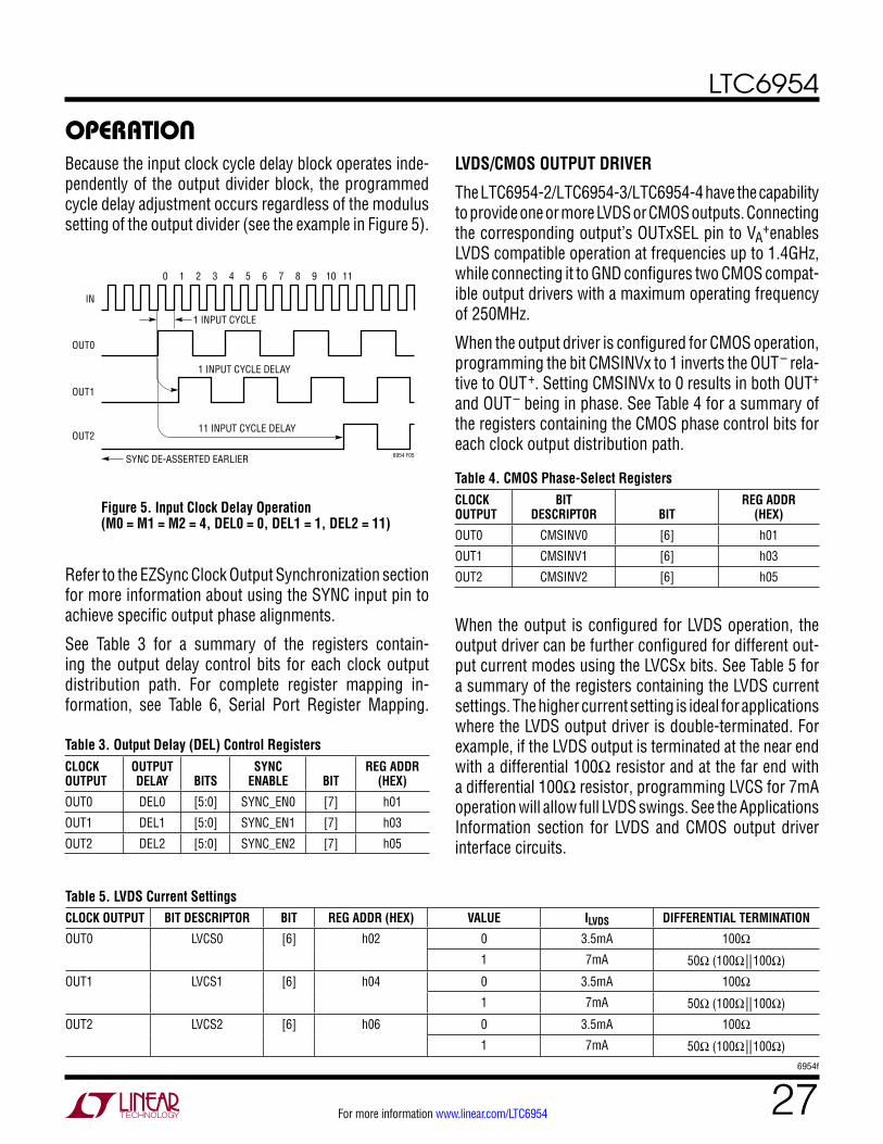
The LTC6954-2/LTC6954-3/LTC6954-4 have the capability to provide one or more LVDS or CMOS outputs. Connecting the corresponding output’s OUTxSEL pin to VA
+enables LVDS compatible operation at frequencies up to 1.4GHz, while connecting it to GND configures two CMOS compat-ible output drivers with a maximum operating frequency of 250MHz.
When the output driver is configured for CMOS operation, programming the bit CMSINVx to 1 inverts the OUT– rela-tive to OUT+. Setting CMSINVx to 0 results in both OUT+ and OUT– being in phase. See Table 4 for a summary of the registers containing the CMOS phase control bits for each clock output distribution path.
Table 4. CMOS Phase-Select Registers CLOCK OUTPUT
BIT DESCRIPTOR BIT
REG ADDR (HEX)
OUT0 CMSINV0 [6] h01
OUT1 CMSINV1 [6] h03
OUT2 CMSINV2 [6] h05
When the output is configured for LVDS operation, the output driver can be further configured for different out-put current modes using the LVCSx bits. See Table 5 for a summary of the registers containing the LVDS current settings. The higher current setting is ideal for applications where the LVDS output driver is double-terminated. For example, if the LVDS output is terminated at the near end with a differential 100Ω resistor and at the far end with a differential 100Ω resistor, programming LVCS for 7mA operation will allow full LVDS swings. See the Applications Information section for LVDS and CMOS output driver interface circuits.
Table 5. LVDS Current SettingsCLOCK OUTPUT BIT DESCRIPTOR BIT REG ADDR (HEX) VALUE ILVDS DIFFERENTIAL TERMINATION
OUT0 LVCS0 [6] h02 0 3.5mA 100Ω
1 7mA 50Ω (100Ω||100Ω)
OUT1 LVCS1 [6] h04 0 3.5mA 100Ω
1 7mA 50Ω (100Ω||100Ω)
OUT2 LVCS2 [6] h06 0 3.5mA 100Ω
1 7mA 50Ω (100Ω||100Ω)
LTC6954
286954f
For more information www.linear.com/LTC6954
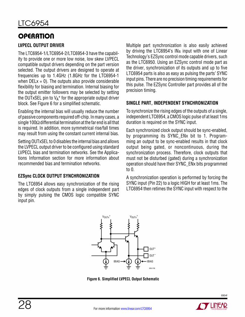
operaTionLVPECL OUTPUT DRIVER
The LTC6954-1/LTC6954-2/LTC6954-3 have the capabil-ity to provide one or more low noise, low skew LVPECL compatible output drivers depending on the part version selected. The output drivers are designed to operate at frequencies up to 1.4GHz (1.8GHz for the LTC6954-1 when DELx = 0). The outputs also provide considerable flexibility for biasing and termination. Internal biasing for the output emitter followers may be selected by setting the OUTxSEL pin to VA
+ for the appropriate output driver block. See Figure 6 for a simplified schematic.
Enabling the internal bias will usually reduce the number of passive components required off-chip. In many cases, a single 100Ω differential termination at the far end is all that is required. In addition, more symmetrical rise/fall times may result from using the constant current internal bias.
Setting OUTxSEL to 0 disables the internal bias and allows the LVPECL output driver to be configured using standard LVPECL bias and termination networks. See the Applica-tions Information section for more information about recommended bias and termination networks.
EZSync CLOCK OUTPUT SYNCHRONIZATION
The LTC6954 allows easy synchronization of the rising edges of clock outputs from a single independent part by simply pulsing the CMOS logic compatible SYNC input pin.
Multiple part synchronization is also easily achieved by driving the LTC6954’s IN± input with one of Linear Technology’s EZSync control mode capable drivers, such as the LTC6950. Using an EZSync control mode part as the driver, synchronization of its outputs and up to five LTC6954 parts is also as easy as pulsing the parts’ SYNC input pins. There are no precision timing requirements for this pulse. The EZSync Controller part provides all of the precision timing.
SINGLE PART, INDEPENDENT SYNCHRONIZATION
To synchronize the rising edges of the outputs of a single, independent LTC6954, a CMOS logic pulse of at least 1ms duration is required on the SYNC input.
Each synchronized clock output should be sync-enabled, by programming its SYNC_ENx bit to 1. Program-ming an output to be sync-enabled results in that clock output being gated, or noncontinuous, during the synchronization process. Therefore, clock outputs that must not be disturbed (gated) during a synchronization operation should have their SYNC_ENx bits programmed to 0.
A synchronization operation is performed by forcing the SYNC input (Pin 22) to a logic HIGH for at least 1ms. The LTC6954 then retimes the SYNC input with respect to the
OUT+
OUT–
6954 F06
VOUTx+ VOUTx
+
IBIAS IBIAS
Figure 6. Simplified LVPECL Output Schematic
LTC6954
296954f
For more information www.linear.com/LTC6954
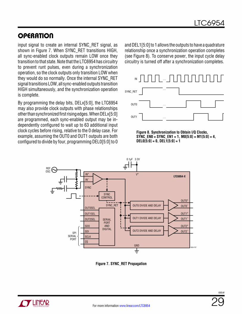
operaTioninput signal to create an internal SYNC_RET signal, as shown in Figure 7. When SYNC_RET transitions HIGH, all sync-enabled clock outputs remain LOW once they transition to that state. Note that the LTC6954 has circuitry to prevent runt pulses, even during a synchronization operation, so the clock outputs only transition LOW when they would do so normally. Once the internal SYNC_RET signal transitions LOW, all sync-enabled outputs transition HIGH simultaneously, and the synchronization operation is complete.
By programming the delay bits, DELx[5:0], the LTC6954 may also provide clock outputs with phase relationships other than synchronized first rising edges. When DELx[5:0] are programmed, each sync-enabled output may be in-dependently configured to wait up to 63 additional input clock cycles before rising, relative to the 0 delay case. For example, assuming the OUT0 and OUT1 outputs are both configured to divide by four, programming DEL0[5:0] to 0
and DEL1[5:0] to 1 allows the outputs to have a quadrature relationship once a synchronization operation completes (see Figure 8). To conserve power, the input cycle delay circuitry is turned off after a synchronization completes.
Figure 7. SYNC_RET Propagation
Figure 8. Synchronization to Obtain I/Q Clocks, SYNC_EN0 = SYNC_EN1 = 1, M0[5:0] = M1[5:0] = 4, DEL0[5:0] = 0, DEL1[5:0] = 1
IN …
…
…
…
6954 F08
SYNC_RET
OUT0
OUT1
LV/CM DIVIDE AND DELAYSYNC_EN4 = 1, FLRDRV = 0OUT2 DIVIDE AND DELAY
OUT1 DIVIDE AND DELAY
OUT0 DIVIDE AND DELAYSYNC_RET
REFOSC
6954 F07
OUT2+
OUT2–
OUT1+
OUT1–
OUT0+
OUT0–
SPISERIAL
PORT
V+
3.3V0.1µF
SCLK
CSGND
SDO
SDI
OUT0SEL
OUT1SEL
OUT2SEL
SYNC
IN+
IN–LTC6954-X
SYNCCONTROL
SERIALPORTAND
DIGITAL
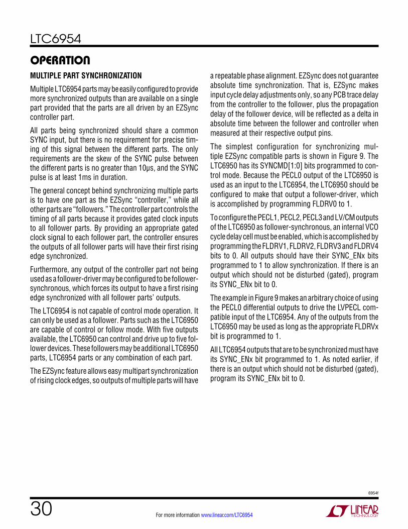
LTC6954
306954f
For more information www.linear.com/LTC6954
operaTionMULTIPLE PART SYNCHRONIZATION
Multiple LTC6954 parts may be easily configured to provide more synchronized outputs than are available on a single part provided that the parts are all driven by an EZSync controller part.
All parts being synchronized should share a common SYNC input, but there is no requirement for precise tim-ing of this signal between the different parts. The only requirements are the skew of the SYNC pulse between the different parts is no greater than 10μs, and the SYNC pulse is at least 1ms in duration.
The general concept behind synchronizing multiple parts is to have one part as the EZSync “controller,” while all other parts are “followers.” The controller part controls the timing of all parts because it provides gated clock inputs to all follower parts. By providing an appropriate gated clock signal to each follower part, the controller ensures the outputs of all follower parts will have their first rising edge synchronized.
Furthermore, any output of the controller part not being used as a follower-driver may be configured to be follower-synchronous, which forces its output to have a first rising edge synchronized with all follower parts’ outputs.
The LTC6954 is not capable of control mode operation. It can only be used as a follower. Parts such as the LTC6950 are capable of control or follow mode. With five outputs available, the LTC6950 can control and drive up to five fol-lower devices. These followers may be additional LTC6950 parts, LTC6954 parts or any combination of each part.
The EZSync feature allows easy multipart synchronization of rising clock edges, so outputs of multiple parts will have
a repeatable phase alignment. EZSync does not guarantee absolute time synchronization. That is, EZSync makes input cycle delay adjustments only, so any PCB trace delay from the controller to the follower, plus the propagation delay of the follower device, will be reflected as a delta in absolute time between the follower and controller when measured at their respective output pins.
The simplest configuration for synchronizing mul-tiple EZSync compatible parts is shown in Figure 9. The LTC6950 has its SYNCMD[1:0] bits programmed to con-trol mode. Because the PECL0 output of the LTC6950 is used as an input to the LTC6954, the LTC6950 should be configured to make that output a follower-driver, which is accomplished by programming FLDRV0 to 1.
To configure the PECL1, PECL2, PECL3 and LV/CM outputs of the LTC6950 as follower-synchronous, an internal VCO cycle delay cell must be enabled, which is accomplished by programming the FLDRV1, FLDRV2, FLDRV3 and FLDRV4 bits to 0. All outputs should have their SYNC_ENx bits programmed to 1 to allow synchronization. If there is an output which should not be disturbed (gated), program its SYNC_ENx bit to 0.
The example in Figure 9 makes an arbitrary choice of using the PECL0 differential outputs to drive the LVPECL com-patible input of the LTC6954. Any of the outputs from the LTC6950 may be used as long as the appropriate FLDRVx bit is programmed to 1.
All LTC6954 outputs that are to be synchronized must have its SYNC_ENx bit programmed to 1. As noted earlier, if there is an output which should not be disturbed (gated), program its SYNC_ENx bit to 0.
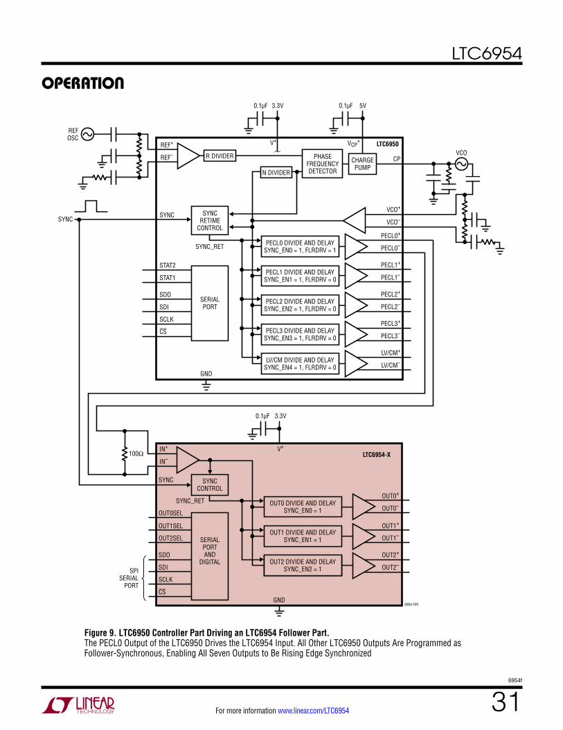
LTC6954
316954f
For more information www.linear.com/LTC6954
operaTion
Figure 9. LTC6950 Controller Part Driving an LTC6954 Follower Part. The PECL0 Output of the LTC6950 Drives the LTC6954 Input. All Other LTC6950 Outputs Are Programmed as Follower-Synchronous, Enabling All Seven Outputs to Be Rising Edge Synchronized
LV/CM DIVIDE AND DELAYSYNC_EN4 = 1, FLRDRV = 0OUT2 DIVIDE AND DELAY
SYNC_EN2 = 1
OUT1 DIVIDE AND DELAYSYNC_EN1 = 1
OUT0 DIVIDE AND DELAYSYNC_EN0 = 1
SYNC_RET
REFOSC
VCP+
SCLK
CS
SDO
SDI
STAT2
STAT1
SYNCSYNC
SERIALPORT
PHASEFREQUENCYDETECTOR
R DIVIDER
REF+
REF–
LTC6950
CP
6954 F09
OUT2+
OUT2–
OUT1+
OUT1–
OUT0+
OUT0–
SPISERIAL
PORT
V+
3.3V0.1µF
SCLK
CSGND
SDO
SDI
OUT0SEL
OUT1SEL
OUT2SEL
SYNC
IN+
IN–LTC6954-X
GND
SYNCCONTROL
SERIALPORTAND
DIGITAL
LV/CM+
LV/CM–LV/CM DIVIDE AND DELAYSYNC_EN4 = 1, FLRDRV = 0
PECL3+
PECL3–PECL3 DIVIDE AND DELAYSYNC_EN3 = 1, FLRDRV = 0
PECL2+
PECL2–PECL2 DIVIDE AND DELAYSYNC_EN2 = 1, FLRDRV = 0
PECL1+
PECL1–PECL1 DIVIDE AND DELAYSYNC_EN1 = 1, FLRDRV = 0
PECL0+
PECL0–PECL0 DIVIDE AND DELAYSYNC_EN0 = 1, FLRDRV = 1
VCO+
V+
VCO–
SYNC_RET
SYNCRETIME
CONTROL
VCOCHARGEPUMP
N DIVIDER
100Ω
0.1µF 5V0.1µF 3.3V
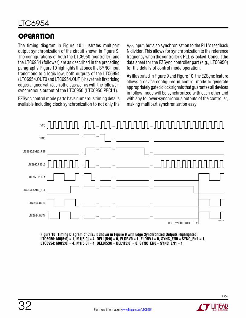
LTC6954
326954f
For more information www.linear.com/LTC6954
operaTionThe timing diagram in Figure 10 illustrates multipart output synchronization of the circuit shown in Figure 9. The configurations of both the LTC6950 (controller) and the LTC6954 (follower) are as described in the preceding paragraphs. Figure 10 highlights that once the SYNC input transitions to a logic low, both outputs of the LTC6954 (LTC6954.OUT0 and LTC6954.OUT1) have their first rising edges aligned with each other, as well as with the follower-synchronous output of the LTC6950 (LTC6950.PECL1).
EZSync control mode parts have numerous timing details available including clock synchronization to not only the
Figure 10. Timing Diagram of Circuit Shown in Figure 9 with Edge Synchronized Outputs Highlighted; LTC6950: M0[5:0] = 1, M1[5:0] = 4, DEL1[5:0] = 0, FLDRV0 = 1, FLDRV1 = 0, SYNC_EN0 = SYNC_EN1 = 1, LTC6954: M0[5:0] = 4, M1[5:0] = 4, DEL0[5:0] = DEL1[5:0] = 0, SYNC_EN0 = SYNC_EN1 = 1
VCO input, but also synchronization to the PLL’s feedback N divider. This allows for synchronization to the reference frequency when the controller’s PLL is locked. Consult the data sheet for the EZSync controller part (e.g., LTC6950) for the details of control mode operation.
As illustrated in Figure 9 and Figure 10, the EZSync feature allows a device configured in control mode to generate appropriately gated clock signals that guarantee all devices in follow mode will be synchronized with each other and with any follower-synchronous outputs of the controller, making multipart synchronization easy.
VCO …
…
…
SYNC
LTC6950.SYNC_RET
LTC6950.PECL0
LTC6950.PECL1
LTC6954.SYNC_RET
LTC6954.OUT0
LTC6954.OUT1
EDGE SYNCHRONIZED
…
6954 F10
…
…
…
…
…
…
…
…
…
…
…
…
…
…
…
…
…
…
…
…
…
…
…
…
…
…
…
…
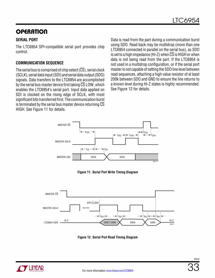
LTC6954
336954f
For more information www.linear.com/LTC6954
operaTionSERIAL PORT
The LTC6954 SPI-compatible serial port provides chip control.
COMMUNICATION SEQUENCE
The serial bus is comprised of chip select (CS), serial clock (SCLK), serial data input (SDI) and serial data output (SDO) signals. Data transfers to the LTC6954 are accomplished by the serial bus master device first taking CS LOW, which enables the LTC6954’s serial port. Input data applied on SDI is clocked on the rising edge of SCLK, with most significant bits transferred first. The communication burst is terminated by the serial bus master device returning CS HIGH. See Figure 11 for details.
Data is read from the part during a communication burst using SDO. Read back may be multidrop (more than one LTC6954 connected in parallel on the serial bus), as SDO is set to a high impedance (Hi-Z) when CS is HIGH or when data is not being read from the part. If the LTC6954 is not used in a multidrop configuration, or if the serial port master is not capable of setting the SDO line level between read sequences, attaching a high value resistor of at least 200k between SDO and GND to ensure the line returns to a known level during Hi-Z states is highly recommended. See Figure 12 for details.
Figure 11. Serial Port Write Timing Diagram
Figure 12. Serial Port Read Timing Diagram
MASTER–CS
MASTER–SCLK
tCSS
tCS tCH
DATA DATA
6954 F11
tCKL tCKH
tCSStCSH
MASTER–SDI
MASTER–CS
MASTER–SCLK
LTC6954–SDOHi-Z Hi-Z
6954 F12
8TH CLOCK
DATADON’T CARE DATA
tDOtDOtDO tDO
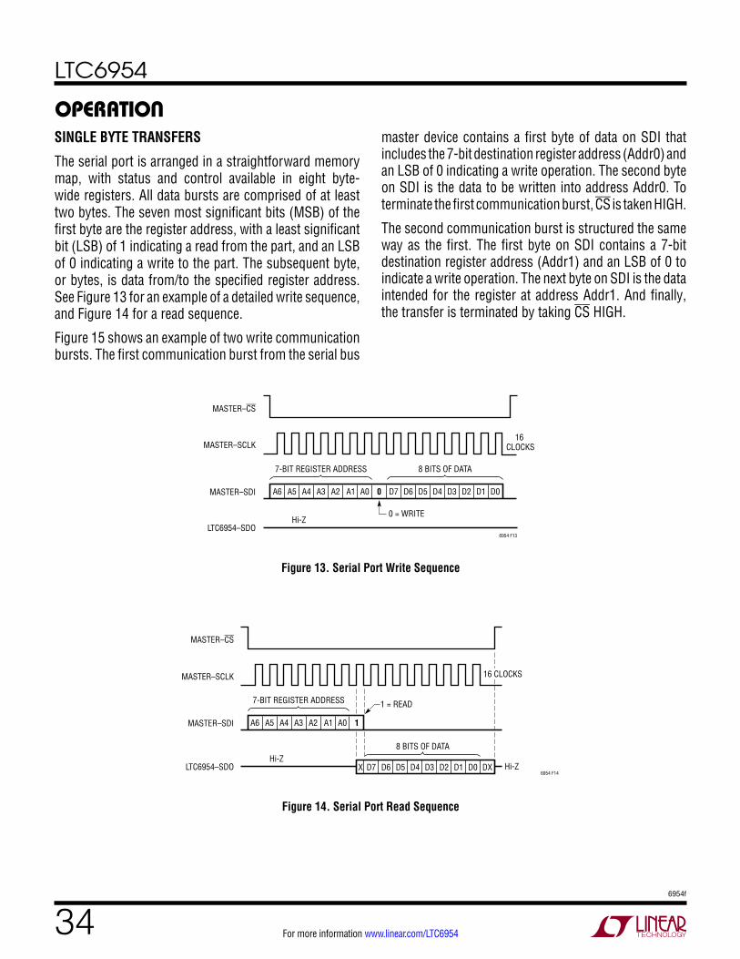
LTC6954
346954f
For more information www.linear.com/LTC6954
operaTionSINGLE BYTE TRANSFERS
The serial port is arranged in a straightforward memory map, with status and control available in eight byte- wide registers. All data bursts are comprised of at least two bytes. The seven most significant bits (MSB) of the first byte are the register address, with a least significant bit (LSB) of 1 indicating a read from the part, and an LSB of 0 indicating a write to the part. The subsequent byte, or bytes, is data from/to the specified register address. See Figure 13 for an example of a detailed write sequence, and Figure 14 for a read sequence.
Figure 15 shows an example of two write communication bursts. The first communication burst from the serial bus
master device contains a first byte of data on SDI that includes the 7-bit destination register address (Addr0) and an LSB of 0 indicating a write operation. The second byte on SDI is the data to be written into address Addr0. To terminate the first communication burst, CS is taken HIGH.
The second communication burst is structured the same way as the first. The first byte on SDI contains a 7-bit destination register address (Addr1) and an LSB of 0 to indicate a write operation. The next byte on SDI is the data intended for the register at address Addr1. And finally, the transfer is terminated by taking CS HIGH.
Figure 13. Serial Port Write Sequence
Figure 14. Serial Port Read Sequence
A6 A5 A4 A3 A2
7-BIT REGISTER ADDRESS
Hi-Z
MASTER–CS
MASTER–SCLK
MASTER–SDI
LTC6954–SDO
A1 A0 0 D7 D6 D5 D4 D3 D2 D1 D0
8 BITS OF DATA
0 = WRITE
6954 F13
16 CLOCKS
A6 A5 A4 A3 A2
7-BIT REGISTER ADDRESS
Hi-ZHi-Z
A1 A0 1
D7X D6 D5 D4 D3 D2 D1 D0 DX
8 BITS OF DATA
1 = READ
6954 F14
MASTER–CS
MASTER–SCLK
MASTER–SDI
LTC6954–SDO
16 CLOCKS
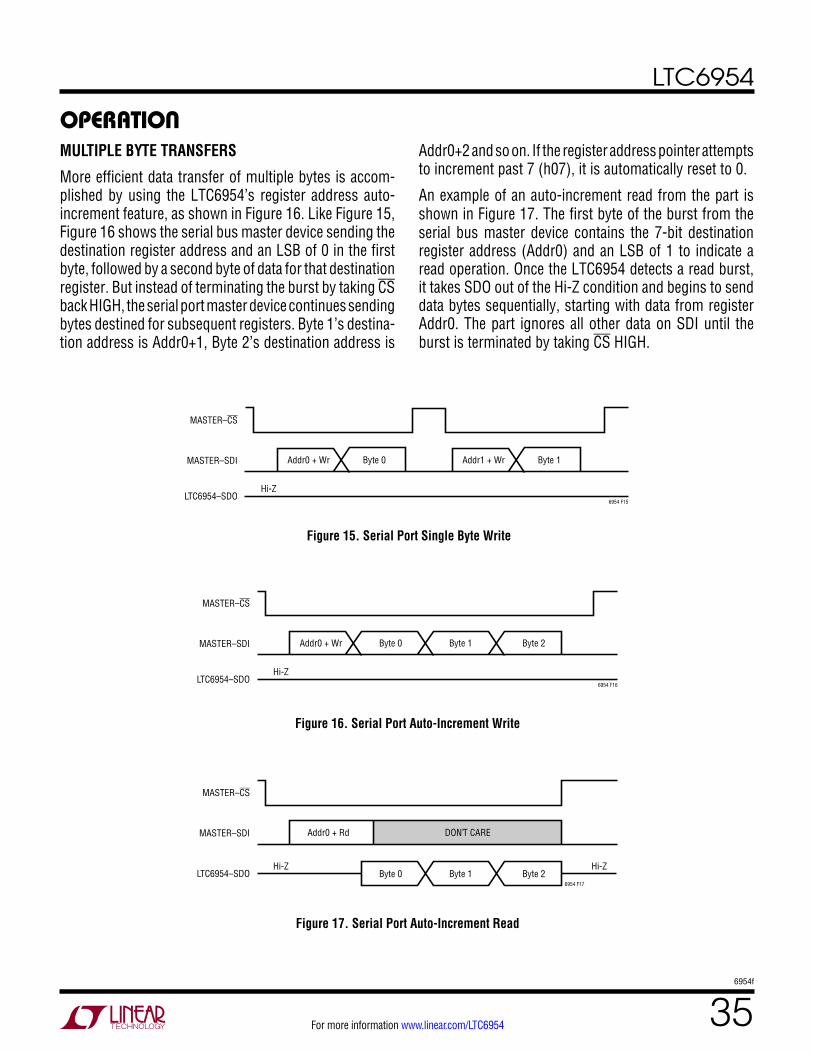
LTC6954
356954f
For more information www.linear.com/LTC6954
operaTion
Figure 15. Serial Port Single Byte Write
Figure 16. Serial Port Auto-Increment Write
Figure 17. Serial Port Auto-Increment Read
MULTIPLE BYTE TRANSFERS
More efficient data transfer of multiple bytes is accom-plished by using the LTC6954’s register address auto-increment feature, as shown in Figure 16. Like Figure 15, Figure 16 shows the serial bus master device sending the destination register address and an LSB of 0 in the first byte, followed by a second byte of data for that destination register. But instead of terminating the burst by taking CS back HIGH, the serial port master device continues sending bytes destined for subsequent registers. Byte 1’s destina-tion address is Addr0+1, Byte 2’s destination address is
Addr0+2 and so on. If the register address pointer attempts to increment past 7 (h07), it is automatically reset to 0.
An example of an auto-increment read from the part is shown in Figure 17. The first byte of the burst from the serial bus master device contains the 7-bit destination register address (Addr0) and an LSB of 1 to indicate a read operation. Once the LTC6954 detects a read burst, it takes SDO out of the Hi-Z condition and begins to send data bytes sequentially, starting with data from register Addr0. The part ignores all other data on SDI until the burst is terminated by taking CS HIGH.
Addr0 + Wr
Hi-Z
MASTER–CS
MASTER–SDI
LTC6954–SDO
Byte 0 Addr1 + Wr Byte 1
6954 F15
Addr0 + Wr
Hi-Z
MASTER–CS
MASTER–SDI
LTC6954–SDO
Byte 0 Byte 1 Byte 2
6954 F16
Addr0 + Rd DON’T CARE
Hi-Z Hi-Z
MASTER–CS
MASTER–SDI
LTC6954–SDO6954 F17
Byte 0 Byte 1 Byte 2
LTC6954
366954f
For more information www.linear.com/LTC6954
operaTion
Table 6. LTC6954 Serial Port Register MappingADDR (HEX) [7] MSB [6] [5] [4] [3] [2] [1] [0] LSB R/W
DEFAULT (HEX)
h00 * PDALL PD_OUT2 PD_DIV2 PD_OUT1 PD_DIV1 PD_OUT0 PD_DIV0 R/W h00
h01 SYNC_EN0 CMSINV0 DEL0[5] DEL0[4] DEL0[3] DEL0[2] DEL0[1] DEL0[0] R/W hC0
h02 * LVCS0 M0[5] M0[4] M0[3] M0[2] M0[1] M0[0] R/W h02
h03 SYNC_EN1 CMSINV1 DEL1[5] DEL1[4] DEL1[3] DEL1[2] DEL1[1] DEL1[0] R/W hC0
h04 * LVCS1 M1[5] M1[4] M1[3] M1[2] M1[1] M1[0] R/W h04
h05 SYNC_EN2 CMSINV2 DEL2[5] DEL2[4] DEL2[3] DEL2[2] DEL2[1] DEL2[0] R/W hC0
h06 * LVCS2 M2[5] M2[4] M2[3] M2[2] M2[1] M2[0] R/W h08
h07 REV2 REV1 REV0 PART4 PART3 PART2 PART1 PART0 R h2X
*Unused
Table 7. Block Power-Down Descriptions BIT NAME DESCRIPTION
PDALL Power-Down Whole Chip
PD_OUT2 Power-Down OUT2 Output Driver
PD_DIV2 Power-Down OUT2 Output Driver and Output Divider
PD_OUT1 Power-Down OUT1 Output Driver
PD_DIV1 Power-Down OUT1 Output Driver and Output Divider
PD_OUT0 Power-Down OUT0 Output Driver
PD_DIV0 Power-Down OUT0 Output Driver and Output Divider
MULTIDROP CONFIGURATION
Several LTC6954’s may share the serial bus. In this multidrop configuration SCLK, SDI and SDO are com-mon between all parts. The serial bus master must use a separate CS for each LTC6954 and ensure that only one device has CS asserted at any time. It is recommended to attach a high value resistor from SDO to GND to ensure the line returns to a known level during Hi-Z states.
SERIAL PORT REGISTERS
The LTC6954’s memory map is shown in Table 6. Detailed bit descriptions are shown in Table 8.
BLOCK POWER-DOWN
The LTC6954 provides considerable flexibility to power down unused blocks. A summary of power-down bits is shown in Table 7. To determine the power savings in shutting down a particular section, consult the Supply Current Delta area of the Electrical Characteristics section.
As noted earlier, to achieve maximum power savings when an LVPECL output is unused and powered down, it is rec-ommended that no terminations or other bias circuitry be connected to the output driver pins.

LTC6954
376954f
For more information www.linear.com/LTC6954
operaTionTable 8. Serial Port Register Bit Descriptions
NAME DESCRIPTION
REG ADDR (HEX) BIT(s)
DEFAULT VALUE
(b: BINARY h: HEX)
CMSINV0 CMOS Output Phase Relationship on OUT0. IF CMSINV0 = 0, Then OUT0+ and OUT0– Are In-Phase; If CMSINV0 = 1, Then OUT0+ and OUT0– Are Inverted Relative to the Other. Ignore if Configured for LVPECL or LVDS.
h01[6] R/W b1
CMSINV1 CMOS Output Phase Relationship on OUT1. IF CMSINV1 = 0, Then OUT1+ and OUT1– Are In-Phase; If CMSINV1 = 1, Then OUT1+ and OUT1– Are Inverted Relative to the Other. Ignore if Configured for LVPECL or LVDS.
h03[6] R/W b1
CMSINV2 CMOS Output Phase Relationship on OUT2; IF CMSINV2 = 0, Then OUT2+ and OUT2– Are In-Phase; If CMSINV2 = 1, Then OUT2+ and OUT2– Are Inverted Relative to the Other. Ignore if Configured for LVPECL or LVDS.
h05[6] R/W b1
DEL0[5:0] Sets the OUT0 Delay Value, 0 ≤ DEL0[5:0] ≤ 63 Input Clock Cycles. h01[5:0] R/W h00
DEL1[5:0] Sets the OUT1 Delay Value, 0 ≤ DEL1[5:0] ≤ 63 Input Clock Cycles. h03[5:0] R/W h00
DEL2[5:0] Sets the OUT2 Delay Value, 0 ≤ DEL2[5:0] ≤ 63 Input Clock Cycles. h05[5:0] R/W h00
LVCS0 Sets the LVDS Output Current for OUT0, (0 = 3.5mA,1 = 7mA). Ignore if the Output Is LVPECL or CMOS.
h02[6] R/W b0
LVCS1 Sets the LVDS Output Current for OUT1, (0 = 3.5mA,1 = 7mA). Ignore if the Output Is LVPECL or CMOS.
h04[6] R/W b0
LVCS2 Sets the LVDS Output Current for OUT2, (0 = 3.5mA,1 = 7mA). Ignore if the Output Is LVPECL or CMOS.
h06[6] R/W b0
M0[5:0] M0[5:0] Sets the OUT0 Output Divider Modulus to Any Integer From 1 to 63. Programming M0[5:0] to a Value of Hex 0 or 1 Results in a Divide Modulus of 1.
h02[5:0] R/W h02
M1[5:0] M1[5:0] Sets the OUT1 Output Divider Modulus to Any Integer From 1 to 63. Programming M1[5:0] to a Value of Hex 0 or 1 Results in a Divide Modulus of 1.
h04[5:0] R/W h04
M2[5:0] M2[5:0] Sets the OUT2 Output Divider Modulus to Any Integer From 1 to 63. Programming M2[5:0] to a Value of Hex 0 or 1 Results in a Divide Modulus of 1.
h06[5:0] R/W h08
PART[4:0] Part code (h00 = LTC6954-1, h01 = LTC6954-2, h02 = LTC6954-3, h03 = LTC6954-4). h07[4:0] R
PDALL For PDALL = 1, the Full Chip Is Powered Down. h00[6] R/W b0
PD_DIV0 For PD_DIV0 = 1, the OUT0 Divider and the Output Buffer Is Powered Down. h00[0] R/W b0
PD_DIV1 For PD_DIV1 = 1, the OUT1 Divider and the Output Buffer Is Powered Down. h00[2] R/W b0
PD_DIV2 For PD_DIV2 = 1, the OUT2 Divider and the Output Buffer Is Powered Down. h00[4] R/W b0
PD_OUT0 For PD_OUT0 = 1, the OUT0 Output Buffer Is Powered Down. h00[1] R/W b0
PD_OUT1 For PD_OUT1 = 1, the OUT1 Output Buffer Is Powered Down. h00[3] R/W b0
PD_OUT2 For PD_OUT2 = 1, the OUT2 Output Buffer Is Powered Down. h00[5] R/W b0
REV[2:0] Part Revision Code. h07[7:5] R b001
SYNC_EN0 For SYNC_EN0 = 1, the OUT0 Output Will Synchronize to the Clock Input During the SYNC Procedure. If SYNC_EN0 = 0, Then the OUT0 Output Ignores the Input to the SYNC Pin.
h01[7] R/W b1
SYNC_EN1 For SYNC_EN1 = 1, the OUT1 Output Will Synchronize to the Clock Input During the SYNC Procedure. If SYNC_EN1 = 0, Then the OUT1 Output Ignores the Input to the SYNC Pin.
h03[7] R/W b1
SYNC_EN2 For SYNC_EN2 = 1, the OUT2 Output Will Synchronize to the Clock Input During the SYNC Procedure. If SYNC_EN2 = 0, Then the OUT2 Output Ignores the Input to the SYNC Pin.
h05[7] R/W b1
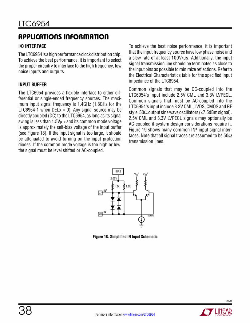
LTC6954
386954f
For more information www.linear.com/LTC6954
applicaTions inForMaTion
Figure 18. Simplified IN Input Schematic
I/O INTERFACE
The LTC6954 is a high performance clock distribution chip. To achieve the best performance, it is important to select the proper circuitry to interface to the high frequency, low noise inputs and outputs.
INPUT BUFFER
The LTC6954 provides a flexible interface to either dif-ferential or single-ended frequency sources. The maxi-mum input signal frequency is 1.4GHz (1.8GHz for the LTC6954-1 when DELx = 0). Any signal source may be directly coupled (DC) to the LTC6954, as long as its signal swing is less than 1.5VP-P and its common mode voltage is approximately the self-bias voltage of the input buffer (see Figure 18). If the input signal is too large, it should be attenuated to avoid turning on the input protection diodes. If the common mode voltage is too high or low, the signal must be level shifted or AC-coupled.
To achieve the best noise performance, it is important that the input frequency source have low phase noise and a slew rate of at least 100V/µs. Additionally, the input signal transmission line should be terminated as close to the input pins as possible to minimize reflections. Refer to the Electrical Characteristics table for the specified input impedance of the LTC6954.
Common signals that may be DC-coupled into the LTC6954’s input include 2.5V CML and 3.3V LVPECL. Common signals that must be AC-coupled into the LTC6954’s input include 3.3V CML, LVDS, CMOS and RF style, 50Ω output sine wave oscillators (<7.5dBm signal). 2.5V CML and 3.3V LVPECL signals may optionally be AC-coupled if system design considerations require it. Figure 19 shows many common IN± input signal inter-faces. Note that all signal traces are assumed to be 50Ω transmission lines.
27
28
1.2kIN+
IN–
1.2k
6954 F18
2.05V
BIASVIN
+ VIN+
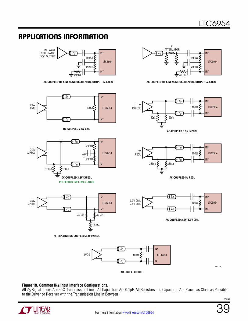
LTC6954
396954f
For more information www.linear.com/LTC6954
applicaTions inForMaTion
Figure 19. Common IN± Input Interface Configurations. All ZO Signal Traces Are 50Ω Transmission Lines. All Capacitors Are 0.1µF. All Resistors and Capacitors Are Placed as Close as Possible to the Driver or Receiver with the Transmission Line in Between
AC-COUPLED 3.3V LVPECL
3.3VLVPECL 100Ω
150Ω 150Ω
ZO
ZO
AC-COUPLED RF SINE WAVE OSCILLATOR, OUTPUT ≤7.5dBm
SINE WAVEOSCILLATOR50Ω OUTPUT 49.9Ω
49.9Ω
49.9Ω
IN+
IN–
LTC6954
IN+
IN–
LTC6954
IN+
IN–
LTC6954
AC-COUPLED 5V PECL
5VPECL 100Ω
330Ω 330Ω
ZO
ZO
IN+
IN–
LTC6954
AC-COUPLED 2.5V/3.3V CML
3.3V CML2.5V CML 100Ω
ZO
ZO
IN+
IN–
LTC6954
AC-COUPLED LVDS
LVDS 100Ω
ZO
ZO
IN+
IN–
LTC6954
DC-COUPLED 3.3V LVPECL
PREFERRED IMPLEMENTATION
3.3VLVPECL
150Ω 150Ω
IN+
IN–
LTC6954
ALTERNATIVE DC-COUPLED 3.3V LVPECL
3.3VLVPECL
49.9Ω 49.9Ω
46.4Ω
ZO
ZO
IN+
IN–
LTC6954
DC-COUPLED 2.5V CML
2.5VCML
ZO
6954 F19
PIATTENUATOR
AC-COUPLED RF SINE WAVE OSCILLATOR, OUTPUT >7.5dBm
49.9Ω
49.9Ω
49.9Ω
ZO
ZO
ZO
49.9Ω
49.9Ω
IN+
IN–
LTC6954
ZO
ZO
100Ω
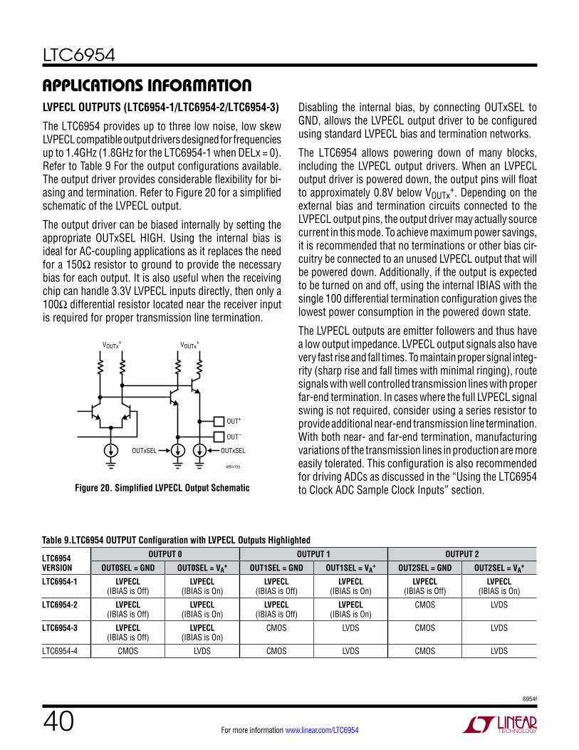
LTC6954
406954f
For more information www.linear.com/LTC6954
applicaTions inForMaTionLVPECL OUTPUTS (LTC6954-1/LTC6954-2/LTC6954-3)
The LTC6954 provides up to three low noise, low skew LVPECL compatible output drivers designed for frequencies up to 1.4GHz (1.8GHz for the LTC6954-1 when DELx = 0). Refer to Table 9 For the output configurations available. The output driver provides considerable flexibility for bi-asing and termination. Refer to Figure 20 for a simplified schematic of the LVPECL output.
The output driver can be biased internally by setting the appropriate OUTxSEL HIGH. Using the internal bias is ideal for AC-coupling applications as it replaces the need for a 150Ω resistor to ground to provide the necessary bias for each output. It is also useful when the receiving chip can handle 3.3V LVPECL inputs directly, then only a 100Ω differential resistor located near the receiver input is required for proper transmission line termination.
Figure 20. Simplified LVPECL Output Schematic
Disabling the internal bias, by connecting OUTxSEL to GND, allows the LVPECL output driver to be configured using standard LVPECL bias and termination networks.
The LTC6954 allows powering down of many blocks, including the LVPECL output drivers. When an LVPECL output driver is powered down, the output pins will float to approximately 0.8V below VOUTx
+. Depending on the external bias and termination circuits connected to the LVPECL output pins, the output driver may actually source current in this mode. To achieve maximum power savings, it is recommended that no terminations or other bias cir-cuitry be connected to an unused LVPECL output that will be powered down. Additionally, if the output is expected to be turned on and off, using the internal IBIAS with the single 100 differential termination configuration gives the lowest power consumption in the powered down state.
The LVPECL outputs are emitter followers and thus have a low output impedance. LVPECL output signals also have very fast rise and fall times. To maintain proper signal integ-rity (sharp rise and fall times with minimal ringing), route signals with well controlled transmission lines with proper far-end termination. In cases where the full LVPECL signal swing is not required, consider using a series resistor to provide additional near-end transmission line termination. With both near- and far-end termination, manufacturing variations of the transmission lines in production are more easily tolerated. This configuration is also recommended for driving ADCs as discussed in the “Using the LTC6954 to Clock ADC Sample Clock Inputs” section.
Table 9.LTC6954 OUTPUT Configuration with LVPECL Outputs Highlighted
LTC6954 VERSION
OUTPUT 0 OUTPUT 1 OUTPUT 2
OUT0SEL = GND OUT0SEL = VA+ OUT1SEL = GND OUT1SEL = VA
+ OUT2SEL = GND OUT2SEL = VA+
LTC6954-1 LVPECL (IBIAS is Off)
LVPECL (IBIAS is On)
LVPECL (IBIAS is Off)
LVPECL (IBIAS is On)
LVPECL (IBIAS is Off)
LVPECL (IBIAS is On)
LTC6954-2 LVPECL (IBIAS is Off)
LVPECL (IBIAS is On)
LVPECL (IBIAS is Off)
LVPECL (IBIAS is On)
CMOS LVDS
LTC6954-3 LVPECL (IBIAS is Off)
LVPECL (IBIAS is On)
CMOS LVDS CMOS LVDS
LTC6954-4 CMOS LVDS CMOS LVDS CMOS LVDS
OUT+
OUT–
6954 F20
VOUTx+ VOUTx
+
OUTxSEL OUTxSEL
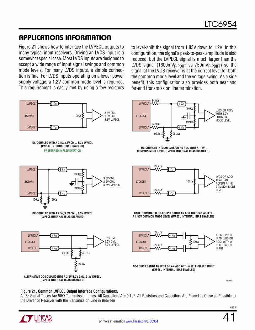
LTC6954
416954f
For more information www.linear.com/LTC6954
applicaTions inForMaTionFigure 21 shows how to interface the LVPECL outputs to many typical input receivers. Driving an LVDS input is a somewhat special case. Most LVDS inputs are designed to accept a wide range of input signal swings and common mode levels. For many LVDS inputs, a simple connec-tion is fine. For LVDS inputs operating on a lower power supply voltage, a 1.2V common mode level is required. This requirement is easily met by using a few resistors
Figure 21. Common LVPECL Output Interface Configurations. All ZO Signal Traces Are 50Ω Transmission Lines. All Capacitors Are 0.1µF. All Resistors and Capacitors Are Placed as Close as Possible to the Driver or Receiver with the Transmission Line in Between
BACK TERMINATED DC-COUPLED INTO AN ADC THAT CAN ACCEPTA 1.85V COMMON MODE LEVEL (LVPECL INTERNAL IBIAS ENABLED)
DC-COUPLED INTO A 2.5V/3.3V CML, 3.3V LVPECL(LVPECL INTERNAL IBIAS DISABLED)
DC-COUPLED INTO AN LVDS OR AN ADC WITH A 1.2V COMMON MODE LEVEL (LVPECL INTERNAL IBIAS DISABLED)
DC-COUPLED INTO A 2.5V/3.3V CML, 3.3V LVPECL(LVPECL INTERNAL IBIAS ENABLED)
PREFERRED IMPLEMENTATION
ALTERNATIVE DC-COUPLED INTO A 2.5V/3.3V CML, 3.3V LVPECL(LVPECL INTERNAL IBIAS DISABLED)
3.3V CML2.5V CML3.3V LVPECL
49.9Ω 49.9Ω
46.4Ω
ZO
ZO
LVPECL+
LVPECL–
LTC6954
AC-COUPLED INTO AN LVDS OR AN ADC WITH A SELF-BIASED INPUT(LVPECL INTERNAL IBIAS ENABLED)
AC-COUPLEDINTO LVDS ORADCs WITH ASELF-BIASEDINPUT
27.4Ω100Ω
27.4ΩZO
ZO
LVPECL+
LVPECL–
LTC6954
6954 F21
LVDS OR ADCs THAT CANACCEPT A 1.8VCOMMON MODELEVEL
LVDS OR ADCs WITH 1.2VCOMMON MODE LEVEL
3.3V CML2.5V CML3.3V LVPECL
LTC69543.3V CML2.5V CML3.3V LVLVPECL
LVPECL+
LVPECL–
150Ω 150Ω
ZO
ZO
49.9Ω
49.9Ω
LTC6954
LVPECL+
LVPECL–
ZO
ZO
100Ω LTC6954
LVPECL+
LVPECL–
95.3Ω 95.3Ω
ZO
ZO
49.9Ω
49.9Ω54.9Ω
54.9Ω
LTC6954
LVPECL+
LVPECL–
ZO
ZO
100Ω
27.4Ω
27.4Ω
to level-shift the signal from 1.85V down to 1.2V. In this configuration, the signal’s peak-to-peak amplitude is also reduced, but the LVPECL signal is much larger than the LVDS signal (1600mVP-PDIFF vs 750mVP-PDIFF) so the signal at the LVDS receiver is at the correct level for both the common mode level and the voltage swing. As a side benefit, this configuration also provides both near and far-end transmission line termination.
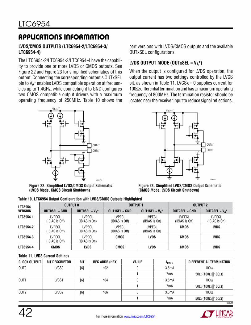
LTC6954
426954f
For more information www.linear.com/LTC6954
applicaTions inForMaTionLVDS/CMOS OUTPUTS (LTC6954-2/LTC6954-3/LTC6954-4)
The LTC6954-2/LTC6954-3/LTC6954-4 have the capabil-ity to provide one or more LVDS or CMOS outputs. See Figure 22 and Figure 23 for simplified schematics of this output. Connecting the corresponding output’s OUTxSEL pin to VA
+ enables LVDS compatible operation at frequen-cies up to 1.4GHz, while connecting it to GND configures two CMOS compatible output drivers with a maximum operating frequency of 250MHz. Table 10 shows the
Table 10. LTC6954 Output Configuration with LVDS/CMOS Outputs Highlighted
LTC6954 VERSION
OUTPUT 0 OUTPUT 1 OUTPUT 2
OUT0SEL = GND OUT0SEL = VA+ OUT1SEL = GND OUT1SEL = VA
+ OUT2SEL = GND OUT2SEL = VA+
LTC6954-1 LVPECL (IBIAS is Off)
LVPECL (IBIAS is On)
LVPECL (IBIAS is Off)
LVPECL (IBIAS is On)
LVPECL (IBIAS is Off)
LVPECL (IBIAS is On)
LTC6954-2 LVPECL (IBIAS is Off)
LVPECL (IBIAS is On)
LVPECL (IBIAS is Off)
LVPECL (IBIAS is On)
CMOS LVDS
LTC6954-3 LVPECL (IBIAS is Off)
LVPECL (IBIAS is On)
CMOS LVDS CMOS LVDS
LTC6954-4 CMOS LVDS CMOS LVDS CMOS LVDS
Figure 22. Simplified LVDS/CMOS Output Schematic (LVDS Mode, CMOS Circuit Shutdown)
Figure 23. Simplified LVDS/CMOS Output Schematic (CMOS Mode, LVDS Circuit Shutdown)
Table 11. LVDS Current SettingsCLOCK OUTPUT BIT DESCRIPTOR BIT REG ADDR (HEX) VALUE ILVDS DIFFERENTIAL TERMINATION
OUT0 LVCS0 [6] h02 0 3.5mA 100Ω
1 7mA 50Ω (100Ω||100Ω)
OUT1 LVCS1 [6] h04 0 3.5mA 100Ω
1 7mA 50Ω (100Ω||100Ω)
OUT2 LVCS2 [6] h06 0 3.5mA 100Ω
1 7mA 50Ω (100Ω||100Ω)
part versions with LVDS/CMOS outputs and the available OUTxSEL configurations.
LVDS OUTPUT MODE (OUTxSEL = VA+)
When the output is configured for LVDS operation, the output current has two settings controlled by the LVCS bit, as shown in Table 11. LVCSx = 0 supplies current for 100Ω differential termination and has a maximum operating frequency of 800MHz. The termination resistor should be located near the receiver input to reduce signal reflections.
VOUTx+
V+
6954 F22
OUTx+
OUTx–
VOUTx+
V+
6954 F23
OUTx+
OUTx–

LTC6954
436954f
For more information www.linear.com/LTC6954
applicaTions inForMaTion
Figure 24. Common LVDS/CMOS Output Interface Configurations. All ZO Signal Traces Are 50Ω Transmission Lines. All Capacitors Are 0.1µF. All Resistors and Capacitors Are Placed as Close as Possible to the Driver or Receiver with the Transmission Line in Between
Setting LVCSx = 1 provides twice the current and enables a maximum operating frequency of 1.4GHz. The higher current setting (ILVDS = 7mA) is ideal for applications where the LVDS output driver is double-terminated (near- and far-end termination). For example, if the LVDS output is terminated at the near end with a differential 100Ω resistor, and at the far end with a differential 100Ω resistor, programming LVCSx = 1 for 7mA operation will allow full LVDS swings. This configuration is properly terminated at both ends, and is therefore more forgiv-ing of the transmission line design and PCB production
variations. Figure 24 shows many common LVDS output interfaces to various logic types of inputs.
Each LVDS output can be independently powered down using the PD_OUTx bit. Refer to Table 6, Serial Port Register Mapping, for the name and location of the power down bits. When the LVDS output is powered down it will be in a Hi-Z state.
When the LVDS/CMOS output is configured to LVDS output mode, the CMSINVx bits are ignored. These bits only apply to a CMOS configured output.
CMOS OUTPUT MODE, AC-COUPLED AND DOUBLY TERMINATED INTO CMOS(SIGNAL SWING AT THE LOAD WILL BE REDUCED)
LVDS OUTPUT MODE, AC-COUPLED INTO LVPECL OR CML (ILVDS = 3.5mA)
THIS CIRCUIT WORKS WITH MANY LVPECLRECEIVER PARTS THAT CAN ACCEPT THE SMALLER LVDS SIGNAL SWING (700mVP-P DIFF FOR LVDS COMPARED TO 1600mVP-P DIFF FOR LVPECL)
3.3VLVPECLCML
3.3V
1.00k 1.00k
680Ω 680Ω
ZO
ZO
LVDS+
LVDS–
LTC6954
LVDS OR ADC100Ω100Ω
100Ω
ZO
ZO
LVDS+
LVDS–
LTC6954
6954 F24
LVDS OUTPUT MODE, DC-COUPLED AND FAR-END TERMINATED INTO LVDS (ILVDS = 3.5mA)
LVDS OUTPUT MODE, DC-COUPLED AND DOUBLY TERMINATED INTO LVDS (ILVDS = 7mA)
LVDS100Ω
ZO
ZO
LVDS+
LVDS–
LTC6954
CMOS
100Ω
100Ω10Ω
ZOCMOS+
V+
CMOS–
LTC6954
CMOS OUTPUT MODE, DC-COUPLED INTO CMOS WITH A SERIES SOURCE TERMINATION
(TRANSMISSION LINE SHOULD BE NO LONGER THAN 10cm)
CMOS10Ω
ZOCMOS+
CMOS–
LTC6954
CMOS OUTPUT MODE, DC-COUPLED AND DOUBLY TERMINATED INTO CMOS(SIGNAL SWING AT THE LOAD WILL BE REDUCED)
CMOS
100Ω
100Ω10Ω
ZOCMOS+
V+
CMOS–
LTC6954
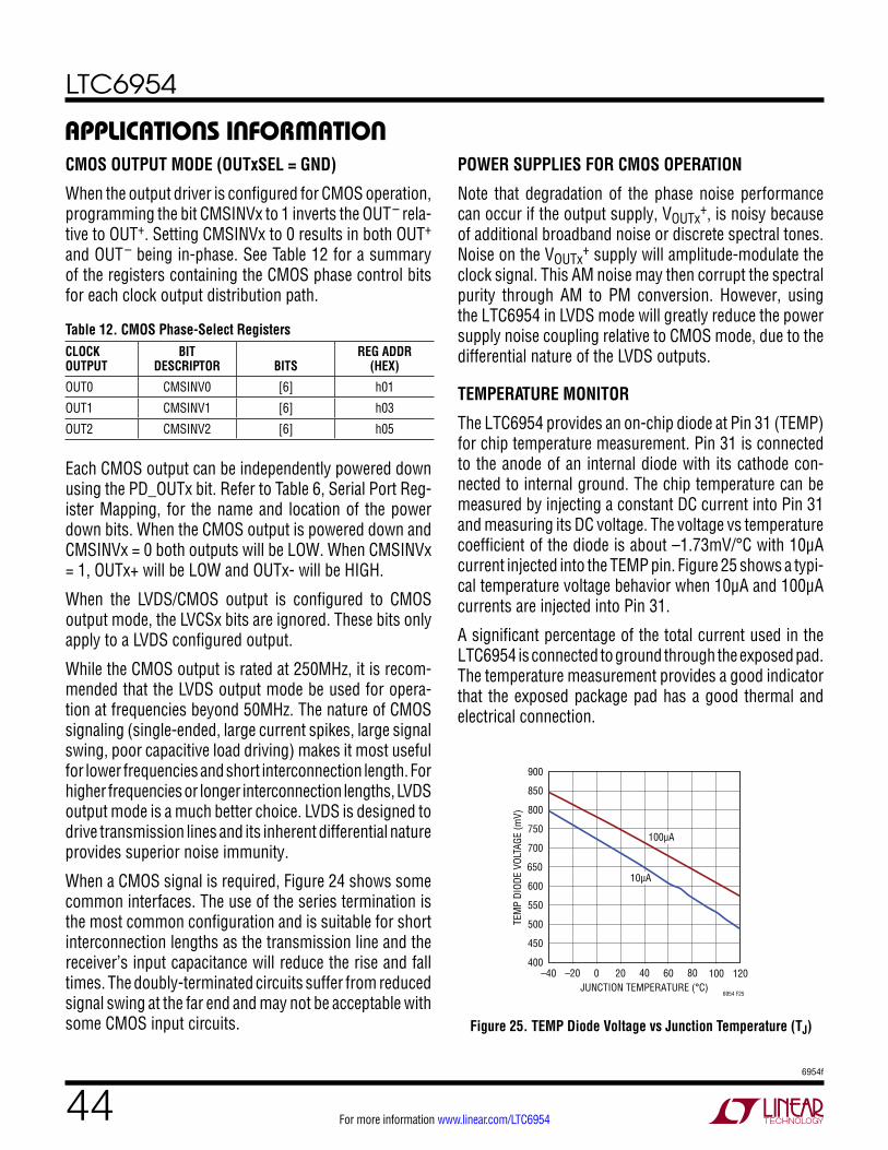
LTC6954
446954f
For more information www.linear.com/LTC6954
applicaTions inForMaTionCMOS OUTPUT MODE (OUTxSEL = GND)
When the output driver is configured for CMOS operation, programming the bit CMSINVx to 1 inverts the OUT– rela-tive to OUT+. Setting CMSINVx to 0 results in both OUT+ and OUT– being in-phase. See Table 12 for a summary of the registers containing the CMOS phase control bits for each clock output distribution path.
Table 12. CMOS Phase-Select Registers CLOCK OUTPUT
BIT DESCRIPTOR BITS
REG ADDR (HEX)
OUT0 CMSINV0 [6] h01
OUT1 CMSINV1 [6] h03
OUT2 CMSINV2 [6] h05
Each CMOS output can be independently powered down using the PD_OUTx bit. Refer to Table 6, Serial Port Reg-ister Mapping, for the name and location of the power down bits. When the CMOS output is powered down and CMSINVx = 0 both outputs will be LOW. When CMSINVx = 1, OUTx+ will be LOW and OUTx- will be HIGH.
When the LVDS/CMOS output is configured to CMOS output mode, the LVCSx bits are ignored. These bits only apply to a LVDS configured output.
While the CMOS output is rated at 250MHz, it is recom-mended that the LVDS output mode be used for opera-tion at frequencies beyond 50MHz. The nature of CMOS signaling (single-ended, large current spikes, large signal swing, poor capacitive load driving) makes it most useful for lower frequencies and short interconnection length. For higher frequencies or longer interconnection lengths, LVDS output mode is a much better choice. LVDS is designed to drive transmission lines and its inherent differential nature provides superior noise immunity.
When a CMOS signal is required, Figure 24 shows some common interfaces. The use of the series termination is the most common configuration and is suitable for short interconnection lengths as the transmission line and the receiver’s input capacitance will reduce the rise and fall times. The doubly-terminated circuits suffer from reduced signal swing at the far end and may not be acceptable with some CMOS input circuits.
POWER SUPPLIES FOR CMOS OPERATION
Note that degradation of the phase noise performance can occur if the output supply, VOUTx
+, is noisy because of additional broadband noise or discrete spectral tones. Noise on the VOUTx
+ supply will amplitude-modulate the clock signal. This AM noise may then corrupt the spectral purity through AM to PM conversion. However, using the LTC6954 in LVDS mode will greatly reduce the power supply noise coupling relative to CMOS mode, due to the differential nature of the LVDS outputs.
TEMPERATURE MONITOR
The LTC6954 provides an on-chip diode at Pin 31 (TEMP) for chip temperature measurement. Pin 31 is connected to the anode of an internal diode with its cathode con-nected to internal ground. The chip temperature can be measured by injecting a constant DC current into Pin 31 and measuring its DC voltage. The voltage vs temperature coefficient of the diode is about –1.73mV/°C with 10μA current injected into the TEMP pin. Figure 25 shows a typi-cal temperature voltage behavior when 10μA and 100μA currents are injected into Pin 31.
A significant percentage of the total current used in the LTC6954 is connected to ground through the exposed pad. The temperature measurement provides a good indicator that the exposed package pad has a good thermal and electrical connection.
Figure 25. TEMP Diode Voltage vs Junction Temperature (TJ)
JUNCTION TEMPERATURE (°C)–40
TEM
P DI
ODE
VOLT
AGE
(mV)
600
850
900
0 40 80
500
750
550
800
450
400
700
650
–20 20 60 100 120
6954 F25
100µA
10µA
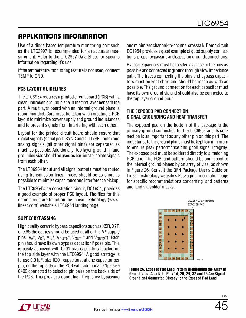
LTC6954
456954f
For more information www.linear.com/LTC6954
applicaTions inForMaTionUse of a diode based temperature monitoring part such as the LTC2997 is recommended for an accurate mea-surement. Refer to the LTC2997 Data Sheet for specific information regarding it’s use.
If the temperature monitoring feature is not used, connect TEMP to GND.
PCB LAYOUT GUIDELINES
The LTC6954 requires a printed circuit board (PCB) with a clean unbroken ground plane in the first layer beneath the part. A multilayer board with an internal ground plane is recommended. Care must be taken when creating a PCB layout to minimize power supply and ground inductances and to prevent signals from interfering with each other.
Layout for the printed circuit board should ensure that digital signals (serial port, SYNC and OUTxSEL pins) and analog signals (all other signal pins) are separated as much as possible. Additionally, top layer ground fill and grounded vias should be used as barriers to isolate signals from each other.
The LTC6954 input and all signal outputs must be routed using transmission lines. Traces should be as short as possible to minimize capacitance and interference pickup.
The LTC6954’s demonstration circuit, DC1954, provides a good example of proper PCB layout. The files for this demo circuit are found on the Linear Technology (www.linear.com) website’s LTC6954 landing page.
SUPPLY BYPASSING
High quality ceramic bypass capacitors such as X5R, X7R or X6S dielectrics should be used at all of the V+ supply pins (VA
+, VD+, VIN
+, VOUT0+, VOUT1
+ and VOUT2+). Each
pin should have its own bypass capacitor if possible. This is easily achieved with 0201 size capacitors located on the top side layer with the LTC6954. A good strategy is to use 0.01µF, size 0201 capacitors, at one capacitor per pin, on the top side of the PCB with additional 0.1µF size 0402 connected to selected pin pairs on the back side of the PCB. This provides good, high frequency bypassing
and minimizes channel-to-channel crosstalk. Demo circuit DC1954 provides a good example of good supply connec-tions, proper bypassing and capacitor ground connections.
Bypass capacitors must be located as close to the pins as possible and connected to ground through a low impedance path. The traces connecting the pins and bypass capaci-tors must be kept short and should be made as wide as possible. The ground connection for each capacitor must have its own ground via and should also be connected to the top layer ground pour.
THE EXPOSED PAD CONNECTION: SIGNAL GROUNDING AND HEAT TRANSFER
The exposed pad on the bottom of the package is the primary ground connection for the LTC6954 and its con-nection is as important as any other pin on this part. The inductance to the ground plane must be kept to a minimum to ensure peak performance and good signal integrity. The exposed pad must be soldered directly to a matching PCB land. The PCB land pattern should be connected to the internal ground planes by an array of vias, as shown in Figure 26. Consult the QFN Package User’s Guide on Linear Technology website’s Packaging Information page for specific recommendations concerning land patterns and land via solder masks.
Figure 26. Exposed Pad Land Pattern Highlighting the Array of Ground Vias. Also Note Pins 14, 26, 29, 32 and 35 Are Signal Ground and Connected Directly to the Exposed Pad Land
18 17 16 15
VIA ARRAY CONNECTSEXPOSED PAD
6954 F2631 32 33 34 35 36
14 13
4
3
2
1
5
6
7
8
9
10
11
12
26
27
28
29
30
25
24
23
22
21
20
19
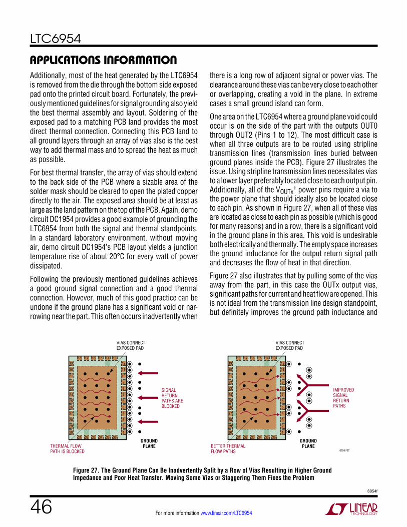
LTC6954
466954f
For more information www.linear.com/LTC6954
applicaTions inForMaTion
Figure 27. The Ground Plane Can Be Inadvertently Split by a Row of Vias Resulting in Higher Ground Impedance and Poor Heat Transfer. Moving Some Vias or Staggering Them Fixes the Problem
Additionally, most of the heat generated by the LTC6954 is removed from the die through the bottom side exposed pad onto the printed circuit board. Fortunately, the previ-ously mentioned guidelines for signal grounding also yield the best thermal assembly and layout. Soldering of the exposed pad to a matching PCB land provides the most direct thermal connection. Connecting this PCB land to all ground layers through an array of vias also is the best way to add thermal mass and to spread the heat as much as possible.
For best thermal transfer, the array of vias should extend to the back side of the PCB where a sizable area of the solder mask should be cleared to open the plated copper directly to the air. The exposed area should be at least as large as the land pattern on the top of the PCB. Again, demo circuit DC1954 provides a good example of grounding the LTC6954 from both the signal and thermal standpoints. In a standard laboratory environment, without moving air, demo circuit DC1954’s PCB layout yields a junction temperature rise of about 20°C for every watt of power dissipated.
Following the previously mentioned guidelines achieves a good ground signal connection and a good thermal connection. However, much of this good practice can be undone if the ground plane has a significant void or nar-rowing near the part. This often occurs inadvertently when
there is a long row of adjacent signal or power vias. The clearance around these vias can be very close to each other or overlapping, creating a void in the plane. In extreme cases a small ground island can form.
One area on the LTC6954 where a ground plane void could occur is on the side of the part with the outputs OUT0 through OUT2 (Pins 1 to 12). The most difficult case is when all three outputs are to be routed using stripline transmission lines (transmission lines buried between ground planes inside the PCB). Figure 27 illustrates the issue. Using stripline transmission lines necessitates vias to a lower layer preferably located close to each output pin. Additionally, all of the VOUTx
+ power pins require a via to the power plane that should ideally also be located close to each pin. As shown in Figure 27, when all of these vias are located as close to each pin as possible (which is good for many reasons) and in a row, there is a significant void in the ground plane in this area. This void is undesirable both electrically and thermally. The empty space increases the ground inductance for the output return signal path and decreases the flow of heat in that direction.
Figure 27 also illustrates that by pulling some of the vias away from the part, in this case the OUTx output vias, significant paths for current and heat flow are opened. This is not ideal from the transmission line design standpoint, but definitely improves the ground path inductance and
18 17 16 15
VIAS CONNECTEXPOSED PAD
GROUNDPLANE
31 32 33 34 35 36
14 13
4
3
2
1
5
6
7
8
9
10
11
12
26
27
28
29
30
25
24
23
22
21
20
1918 17 16 15
SIGNALRETURNPATHS AREBLOCKED
THERMAL FLOW PATH IS BLOCKED
VIAS CONNECTEXPOSED PAD
GROUNDPLANE
6954 F27
IMPROVEDSIGNALRETURNPATHS
BETTER THERMALFLOW PATHS
31 32 33 34 35 36
14 13
4
3
2
1
5
6
7
8
9
10
11
12
26
27
28
29
30
25
24
23
22
21
20
19
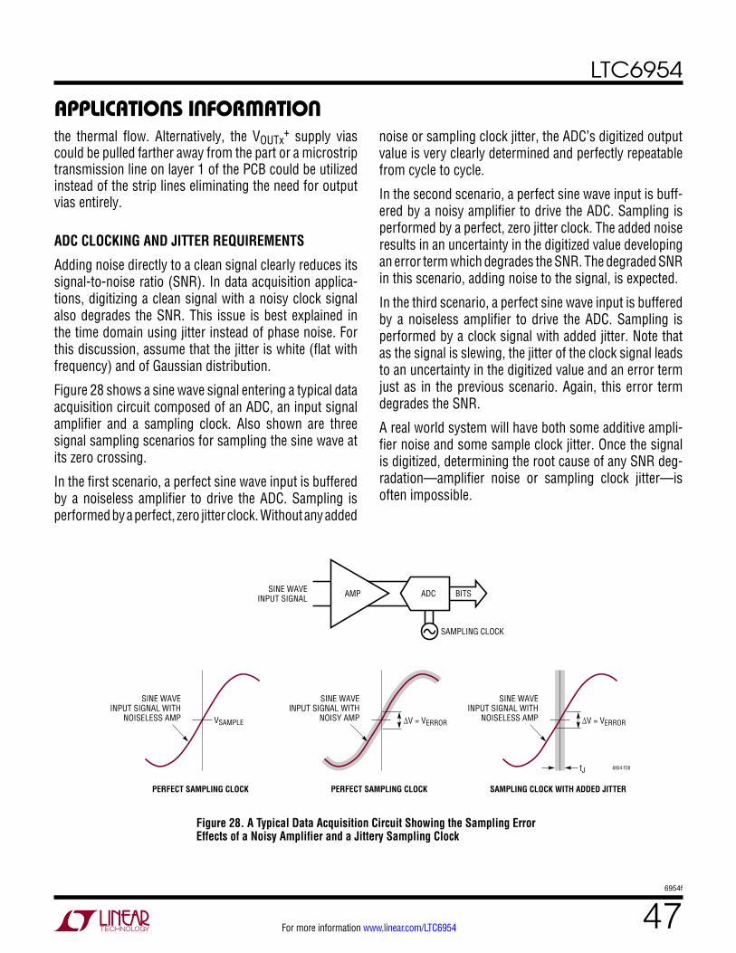
LTC6954
476954f
For more information www.linear.com/LTC6954
applicaTions inForMaTionthe thermal flow. Alternatively, the VOUTx
+ supply vias could be pulled farther away from the part or a microstrip transmission line on layer 1 of the PCB could be utilized instead of the strip lines eliminating the need for output vias entirely.
ADC CLOCKING AND JITTER REQUIREMENTS
Adding noise directly to a clean signal clearly reduces its signal-to-noise ratio (SNR). In data acquisition applica-tions, digitizing a clean signal with a noisy clock signal also degrades the SNR. This issue is best explained in the time domain using jitter instead of phase noise. For this discussion, assume that the jitter is white (flat with frequency) and of Gaussian distribution.
Figure 28 shows a sine wave signal entering a typical data acquisition circuit composed of an ADC, an input signal amplifier and a sampling clock. Also shown are three signal sampling scenarios for sampling the sine wave at its zero crossing.
In the first scenario, a perfect sine wave input is buffered by a noiseless amplifier to drive the ADC. Sampling is performed by a perfect, zero jitter clock. Without any added
noise or sampling clock jitter, the ADC’s digitized output value is very clearly determined and perfectly repeatable from cycle to cycle.
In the second scenario, a perfect sine wave input is buff-ered by a noisy amplifier to drive the ADC. Sampling is performed by a perfect, zero jitter clock. The added noise results in an uncertainty in the digitized value developing an error term which degrades the SNR. The degraded SNR in this scenario, adding noise to the signal, is expected.
In the third scenario, a perfect sine wave input is buffered by a noiseless amplifier to drive the ADC. Sampling is performed by a clock signal with added jitter. Note that as the signal is slewing, the jitter of the clock signal leads to an uncertainty in the digitized value and an error term just as in the previous scenario. Again, this error term degrades the SNR.
A real world system will have both some additive ampli-fier noise and some sample clock jitter. Once the signal is digitized, determining the root cause of any SNR deg-radation—amplifier noise or sampling clock jitter—is often impossible.
Figure 28. A Typical Data Acquisition Circuit Showing the Sampling Error Effects of a Noisy Amplifier and a Jittery Sampling Clock
6954 F28
SINE WAVEINPUT SIGNAL WITH
NOISELESS AMP
SAMPLING CLOCK WITH ADDED JITTER
∆V = VERROR
tJ
SINE WAVEINPUT SIGNAL WITH
NOISY AMP
SINE WAVEINPUT SIGNAL
PERFECT SAMPLING CLOCK
∆V = VERROR
SINE WAVEINPUT SIGNAL WITH
NOISELESS AMP
PERFECT SAMPLING CLOCK
VSAMPLE
SAMPLING CLOCK
BITSADCAMP
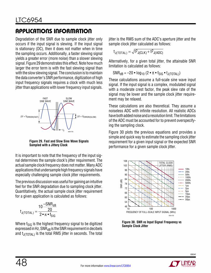
LTC6954
486954f
For more information www.linear.com/LTC6954
applicaTions inForMaTionDegradation of the SNR due to sample clock jitter only occurs if the input signal is slewing. If the input signal is stationary (DC), then it does not matter when in time the sampling occurs. Additionally, a faster slewing signal yields a greater error (more noise) than a slower slewing signal. Figure 29 demonstrates this effect. Note how much larger the error term is with the fast slewing signal than with the slow slewing signal. The conclusion is to maintain the data converter’s SNR performance, digitization of high input frequency signals requires a clock with much less jitter than applications with lower frequency input signals.
It is important to note that the frequency of the input sig-nal determines the sample clock’s jitter requirement. The actual sample clock frequency does not matter. Many ADC applications that undersample high frequency signals have especially challenging sample clock jitter requirements.
The previous discussion was useful for gaining an intuitive feel for the SNR degradation due to sampling clock jitter. Quantitatively, the actual sample clock jitter requirement for a given application is calculated as follows:
tJ(TOTAL) =
10–SNRdB
202 • π • fSIG
Where fSIG is the highest frequency signal to be digitized expressed in Hz, SNRdB is the SNR requirement in decibels and tJ(TOTAL) is the total RMS jitter in seconds. The total
Figure 29. Fast and Slow Sine Wave Signals Sampled with a Jittery Clock
jitter is the RMS sum of the ADC’s aperture jitter and the sample clock jitter calculated as follows:
tJ(TOTAL) = t2J(CLK) + t2J(ADC)
Alternatively, for a given total jitter, the attainable SNR limitation is calculated as follows:
SNRdB = –20 • Iog10 (2 • π • fSIG • tJ(TOTAL))
These calculations assume a full-scale sine wave input signal. If the input signal is a complex, modulated signal with a moderate crest factor, the peak slew rate of the signal may be lower and the sample clock jitter require-ment may be relaxed.
These calculations are also theoretical. They assume a noiseless ADC with infinite resolution. All realistic ADCs have both added noise and a resolution limit. The limitations of the ADC must be accounted for to prevent overspecify-ing the sampling clock.
Figure 30 plots the previous equations and provides a simple and quick way to estimate the sampling clock jitter requirement for a given input signal or the expected SNR performance for a given sample clock jitter.
Figure 30. SNR vs Input Signal Frequency vs Sample Clock Jitter
6954 F29tJ
∆V = VERROR(SLOW)∆V = VERROR(FAST)
FASTSINE WAVE
SLOWSINE WAVE
FREQUENCY OF FULL-SCALE INPUT SIGNAL (MHz)
SNR
(dB)
6954 F30
10 100 1000
108
54
102
90
78
66
96
84
72
60
48
TOTAL CLOCKJITTER (RMS)
10fs20fs50fs100fs200fs500fs1ps2ps5ps10ps20ps50ps
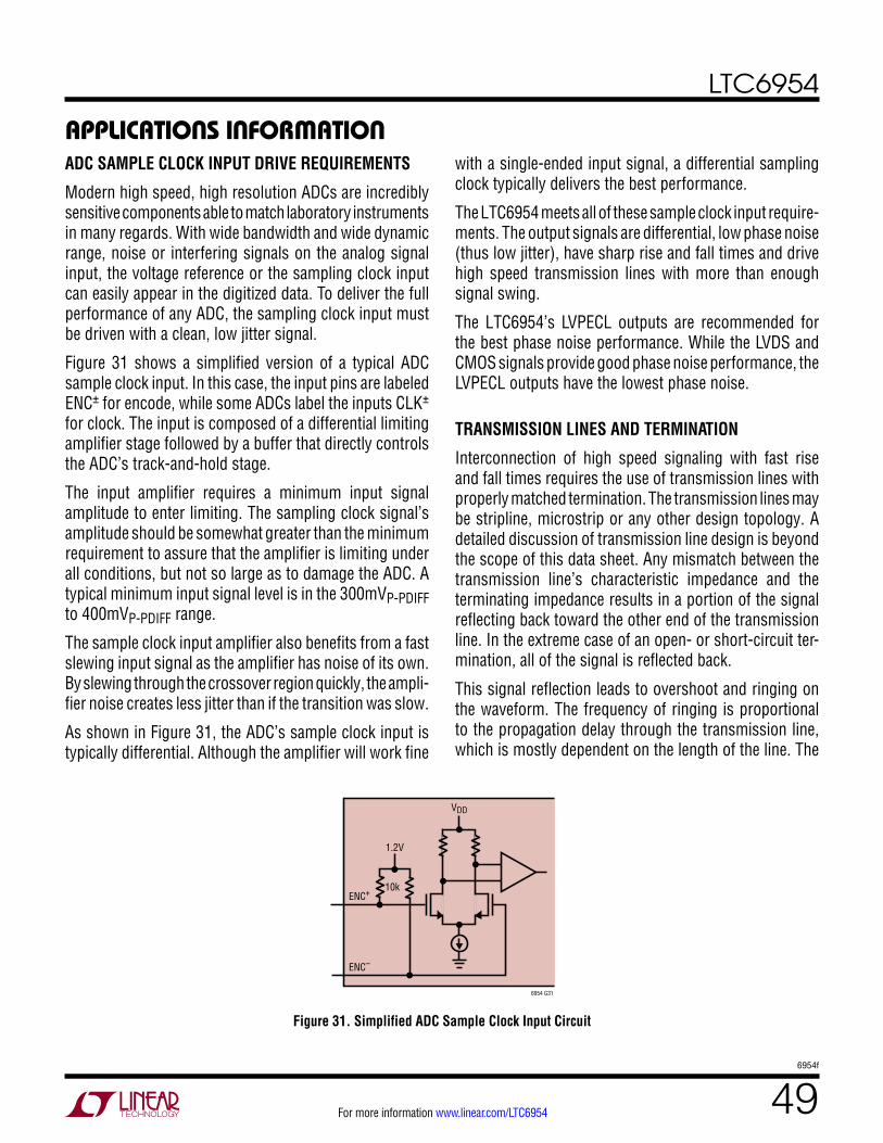
LTC6954
496954f
For more information www.linear.com/LTC6954
applicaTions inForMaTionADC SAMPLE CLOCK INPUT DRIVE REQUIREMENTS
Modern high speed, high resolution ADCs are incredibly sensitive components able to match laboratory instruments in many regards. With wide bandwidth and wide dynamic range, noise or interfering signals on the analog signal input, the voltage reference or the sampling clock input can easily appear in the digitized data. To deliver the full performance of any ADC, the sampling clock input must be driven with a clean, low jitter signal.
Figure 31 shows a simplified version of a typical ADC sample clock input. In this case, the input pins are labeled ENC± for encode, while some ADCs label the inputs CLK±
for clock. The input is composed of a differential limiting amplifier stage followed by a buffer that directly controls the ADC’s track-and-hold stage.
The input amplifier requires a minimum input signal amplitude to enter limiting. The sampling clock signal’s amplitude should be somewhat greater than the minimum requirement to assure that the amplifier is limiting under all conditions, but not so large as to damage the ADC. A typical minimum input signal level is in the 300mVP-PDIFF to 400mVP-PDIFF range.
The sample clock input amplifier also benefits from a fast slewing input signal as the amplifier has noise of its own. By slewing through the crossover region quickly, the ampli-fier noise creates less jitter than if the transition was slow.
As shown in Figure 31, the ADC’s sample clock input is typically differential. Although the amplifier will work fine
with a single-ended input signal, a differential sampling clock typically delivers the best performance.
The LTC6954 meets all of these sample clock input require-ments. The output signals are differential, low phase noise (thus low jitter), have sharp rise and fall times and drive high speed transmission lines with more than enough signal swing.
The LTC6954’s LVPECL outputs are recommended for the best phase noise performance. While the LVDS and CMOS signals provide good phase noise performance, the LVPECL outputs have the lowest phase noise.
TRANSMISSION LINES AND TERMINATION
Interconnection of high speed signaling with fast rise and fall times requires the use of transmission lines with properly matched termination. The transmission lines may be stripline, microstrip or any other design topology. A detailed discussion of transmission line design is beyond the scope of this data sheet. Any mismatch between the transmission line’s characteristic impedance and the terminating impedance results in a portion of the signal reflecting back toward the other end of the transmission line. In the extreme case of an open- or short-circuit ter-mination, all of the signal is reflected back.
This signal reflection leads to overshoot and ringing on the waveform. The frequency of ringing is proportional to the propagation delay through the transmission line, which is mostly dependent on the length of the line. The
Figure 31. Simplified ADC Sample Clock Input Circuit
VDD
6954 G31
1.2V
10kENC+
ENC–

LTC6954
506954f
For more information www.linear.com/LTC6954
applicaTions inForMaTionamplitude of the ringing is dependent on the degree of mismatch between the transmission line’s characteristic impedance and the termination impedance at each end of the line. The greater the mismatch, the larger the reflection and the greater the amplitude of the ringing. Figure 32 shows three methods of transmission line termination with a low impedance driver and a high impedance receiver.
being re-reflected back to the receiver. The far-end receiver is a high impedance and is poorly matched to the trans-mission line resulting in most of the signal being reflected back to the driver. The termination at the source absorbs most of this reflected signal, but if there is a mismatch in the impedance, some of the signal is re-reflected back to the receiver. This back-and-forth signaling continues until the reflected signal energy eventually dies out.
Near- and far-end termination is sometimes referred to as double termination. The advantage of double termina-tion over the simpler far-end or near-end termination is if there is any mismatch at the far end, its reflection will be largely absorbed by the near-end termination and the reflected energy dies out rapidly as each re-reflected signal is considerably smaller at each turn.
The disadvantage of double termination is that the sig-nal level at the receiver is only half the amplitude of the source’s signal. However, this loss of signal amplitude is acceptable in many cases. The series resistor used in near-end termination also adds some noise to the signal.
Double termination makes for a more robust and forgiv-ing system design. Production variation of the printed circuit board (PCB) that would affect the transmission line’s characteristic impedance are more easily accom-modated. Variation of the termination resistor value and its nonidealities are also less critical. Delivering good signal integrity is more easily achieved with double termination of transmission lines at the cost of some added noise.
ADC SAMPLE CLOCK INPUT SIGNAL INTEGRITY REQUIREMENTS
Figure 31 is a simplified ADC sample clock input circuit. The simplification omits many of the circuit details and also omits parasitic elements in the circuit. These parasitic elements play an important role in the ADC’s sample clock input signal integrity requirements.
Logic applications tolerate signal overshoot and ringing to a very high level. For a logic system to work properly, the only requirement is that logic 0 and logic 1 states are separable. A logic 0 or logic 1 state signal with large amounts of ringing, ripple and interference causes little concern in a logic system.
Figure 32. Transmission Line Termination Methods (ZO = 50Ω)
6954 F32
NEAR AND FAR END TERMINATION(DOUBLE TERMINATION)
100Ω50Ω
50ΩZO
ZO
NEAR END TERMINATION(SERIES TERMINATION)
50Ω
50ΩZO
ZO
FAR END TERMINATION(PARALLEL OR SHUNT TERMINATION)
100Ω
ZO
ZO
Far-end termination is sometimes referred to as parallel or shunt termination of the transmission line. Its purpose is to match the transmission line’s impedance and prevent signal reflection back to the driver. Any mismatch at the far end results in a portion of the initial signal being reflected back to the driver. As the low impedance driver is poorly matched to the transmission line, most of this reflected signal is re-reflected back to the receiver. This back and forth signaling continues until the reflected signal energy eventually dies out.
Near-end termination is sometimes referred to as series or back termination. Its purpose is to match the transmission line and prevent any reflected signal from the far end from
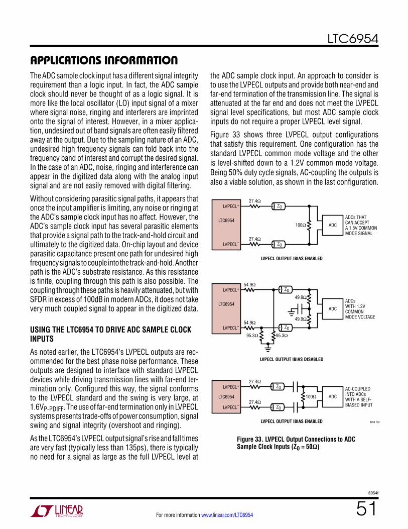
LTC6954
516954f
For more information www.linear.com/LTC6954
applicaTions inForMaTionThe ADC sample clock input has a different signal integrity requirement than a logic input. In fact, the ADC sample clock should never be thought of as a logic signal. It is more like the local oscillator (LO) input signal of a mixer where signal noise, ringing and interferers are imprinted onto the signal of interest. However, in a mixer applica-tion, undesired out of band signals are often easily filtered away at the output. Due to the sampling nature of an ADC, undesired high frequency signals can fold back into the frequency band of interest and corrupt the desired signal. In the case of an ADC, noise, ringing and interference can appear in the digitized data along with the analog input signal and are not easily removed with digital filtering.
Without considering parasitic signal paths, it appears that once the input amplifier is limiting, any noise or ringing at the ADC’s sample clock input has no affect. However, the ADC’s sample clock input has several parasitic elements that provide a signal path to the track-and-hold circuit and ultimately to the digitized data. On-chip layout and device parasitic capacitance present one path for undesired high frequency signals to couple into the track-and-hold. Another path is the ADC’s substrate resistance. As this resistance is finite, coupling through this path is also possible. The coupling through these paths is heavily attenuated, but with SFDR in excess of 100dB in modern ADCs, it does not take very much coupled signal to appear in the digitized data.
USING THE LTC6954 TO DRIVE ADC SAMPLE CLOCK INPUTS
As noted earlier, the LTC6954’s LVPECL outputs are rec-ommended for the best phase noise performance. These outputs are designed to interface with standard LVPECL devices while driving transmission lines with far-end ter-mination only. Configured this way, the signal conforms to the LVPECL standard and the swing is very large, at 1.6VP-PDIFF. The use of far-end termination only in LVPECL systems presents trade-offs of power consumption, signal swing and signal integrity (overshoot and ringing).
As the LTC6954’s LVPECL output signal’s rise and fall times are very fast (typically less than 135ps), there is typically no need for a signal as large as the full LVPECL level at
the ADC sample clock input. An approach to consider is to use the LVPECL outputs and provide both near-end and far-end termination of the transmission line. The signal is attenuated at the far end and does not meet the LVPECL signal level specifications, but most ADC sample clock inputs do not require a proper LVPECL level signal.
Figure 33 shows three LVPECL output configurations that satisfy this requirement. One configuration has the standard LVPECL common mode voltage and the other is level-shifted down to a 1.2V common mode voltage. Being 50% duty cycle signals, AC-coupling the outputs is also a viable solution, as shown in the last configuration.
Figure 33. LVPECL Output Connections to ADC Sample Clock Inputs (ZO = 50Ω)
27.4Ω100Ω
27.4ΩZO
ZO
LVPECL+
LVPECL–
LTC6954
27.4Ω
27.4ΩZO
ZO
LVPECL+
LVPECL–
LTC6954
6954 F33LVPECL OUTPUT IBIAS ENABLED
AC-COUPLEDINTO ADCs WITH A SELF- BIASED INPUT
LVPECL OUTPUT IBIAS ENABLED
ADCs THATCAN ACCEPTA 1.8V COMMONMODE SIGNAL
LVPECL OUTPUT IBIAS DISABLED
ADC
ADC
100Ω
54.9Ω
54.9ΩZO
ZO
LVPECL+
LVPECL–
LTC6954ADCsWITH 1.2V COMMONMODE VOLTAGE
ADC
49.9Ω
49.9Ω
95.3Ω95.3Ω
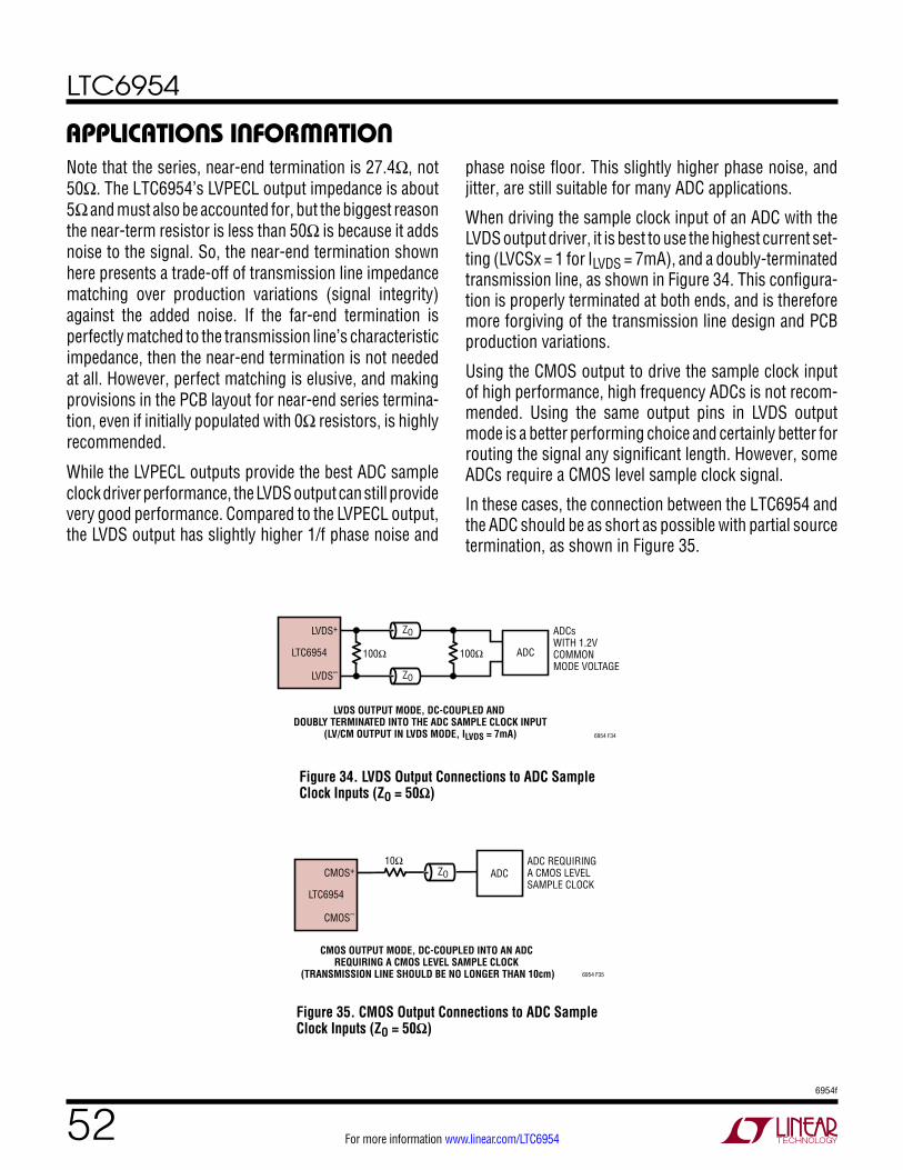
LTC6954
526954f
For more information www.linear.com/LTC6954
applicaTions inForMaTionNote that the series, near-end termination is 27.4Ω, not 50Ω. The LTC6954’s LVPECL output impedance is about 5Ω and must also be accounted for, but the biggest reason the near-term resistor is less than 50Ω is because it adds noise to the signal. So, the near-end termination shown here presents a trade-off of transmission line impedance matching over production variations (signal integrity) against the added noise. If the far-end termination is perfectly matched to the transmission line’s characteristic impedance, then the near-end termination is not needed at all. However, perfect matching is elusive, and making provisions in the PCB layout for near-end series termina-tion, even if initially populated with 0Ω resistors, is highly recommended.
While the LVPECL outputs provide the best ADC sample clock driver performance, the LVDS output can still provide very good performance. Compared to the LVPECL output, the LVDS output has slightly higher 1/f phase noise and
Figure 34. LVDS Output Connections to ADC Sample Clock Inputs (ZO = 50Ω)
Figure 35. CMOS Output Connections to ADC Sample Clock Inputs (ZO = 50Ω)
phase noise floor. This slightly higher phase noise, and jitter, are still suitable for many ADC applications.
When driving the sample clock input of an ADC with the LVDS output driver, it is best to use the highest current set-ting (LVCSx = 1 for ILVDS = 7mA), and a doubly-terminated transmission line, as shown in Figure 34. This configura-tion is properly terminated at both ends, and is therefore more forgiving of the transmission line design and PCB production variations.
Using the CMOS output to drive the sample clock input of high performance, high frequency ADCs is not recom-mended. Using the same output pins in LVDS output mode is a better performing choice and certainly better for routing the signal any significant length. However, some ADCs require a CMOS level sample clock signal.
In these cases, the connection between the LTC6954 and the ADC should be as short as possible with partial source termination, as shown in Figure 35.
6954 F34
100Ω100Ω
ZO
ZO
LVDS+
LVDS–
LTC6954
LVDS OUTPUT MODE, DC-COUPLED AND DOUBLY TERMINATED INTO THE ADC SAMPLE CLOCK INPUT
(LV/CM OUTPUT IN LVDS MODE, ILVDS = 7mA)
ADCsWITH 1.2V COMMONMODE VOLTAGE
ADC
CMOS OUTPUT MODE, DC-COUPLED INTO AN ADC REQUIRING A CMOS LEVEL SAMPLE CLOCK
(TRANSMISSION LINE SHOULD BE NO LONGER THAN 10cm)
10ΩZOCMOS+
CMOS–
LTC6954
6954 F35
ADC REQUIRINGA CMOS LEVELSAMPLE CLOCK
ADC
LTC6954
536954f
For more information www.linear.com/LTC6954
Typical applicaTions
Figure 36. LTC6954 Driving the Encode Sample Clock Input of an LTC2165, 125Msps, 16-Bit ADC
T1: MACOM ETC1-1-13RESISTORS, CAPACITORS ARE 0402 PACKAGE SIZECN1: 2.2µF LOW INDUCTANCEINTERDIGITATED CAPACITORTDK CLLE1AX780G225MMURATA LLA219C70G225MAVX W2L14Z225MOR EQUIVALENT
VCM
AIN+
AIN–
GND
REFH
REFL
REFH
REFL
PAR/SER
GND
GND
VDD
PAR/SER
D11
D10
D9
D8
OVDD
OGND
CLKOUT+
CLKOUT–
D7
D6
D5
D4
1
2
3
4
5
6
7
8
9
10
11
12
36
35
34
33
32
31
30
29
28
27
26
25
SPIPORT
GND ENC+ ENC– CS SCK SDIVDD1.8V
D0 D1 D2 D3
24232221191817161514
37383940414243444647 4548
13
VDD
1.8V
VDD SENSE VREF SDO
SDO
GND OF D15DNC D14 D13 D12
1.8V
C370.1µF
LTC2165
0.1µF
C210.1µF
C180.1µF
GND
20
SENSE
DIGITALOUTPUTS
C320.1µF
R51100Ω
C280.1µF
C190.1µF
C232.2µF
0.1µF
0.1µF
0.1µF
0.1µF +–+–
–+–+
CN1
25Ω
25Ω
50Ω
T1
ANALOGINPUT
315.5MHz–1dBFS
6954 F36
OUT2+
OUT2–
OUT1+
OUT1–
OUT0+
100MHzOUT0–
SPISERIAL
PORT
DEL = 0
V+
3.3V
SCLK
CS
GND
SDO
SDI
OUT0SEL
OUT1SEL
OUT2SEL
SYNC
IN+
IN– LTC6954-3
1GHz
49.9Ω
49.9Ω
100pF
100pF
100pF 49.9Ω
SYNCCONTROL
3.3V0.1µF
SERIALPORTAND
DIGITAL
DIV = 10
DELAY0 TO 63
DIVIDE1 TO 63
DELAY0 TO 63
DIVIDE1 TO 63
LTC6954
546954f
For more information www.linear.com/LTC6954
Typical applicaTions
Figure 37. LTC2165 64k Point FFT, fIN = 315MHz, –1dBFS, 100Msps. Sample Clock Provided by the LTC6954 at 100MHz
FREQUENCY (MHz)0
–100–110–120
–70
–60
–80–90
AMPL
ITUD
E (d
BFS)
–50
–30
–40
–20
–10
0
10 20 30 40 50
6954 F37
TOTAL SYSTEM SNR = 68.8dBLTC6954 JITTER = 113fsRMS
LTC6954
556954f
For more information www.linear.com/LTC6954
Information furnished by Linear Technology Corporation is believed to be accurate and reliable. However, no responsibility is assumed for its use. Linear Technology Corporation makes no representa-tion that the interconnection of its circuits as described herein will not infringe on existing patent rights.
package DescripTionPlease refer to http://www.linear.com/product/LTC6954#packaging for the most recent package drawings.
4.00 ±0.10 2.50 REF
7.00 ±0.10
NOTE:1. DRAWING IS NOT A JEDEC PACKAGE OUTLINE2. DRAWING NOT TO SCALE3. ALL DIMENSIONS ARE IN MILLIMETERS4. DIMENSIONS OF EXPOSED PAD ON BOTTOM OF PACKAGE DO NOT INCLUDE MOLD FLASH. MOLD FLASH, IF PRESENT, SHALL NOT EXCEED 0.20mm ON ANY SIDE5. EXPOSED PAD SHALL BE SOLDER PLATED6. SHADED AREA IS ONLY A REFERENCE FOR PIN 1 LOCATION ON THE TOP AND BOTTOM OF PACKAGE
PIN 1TOP MARK(NOTE 6)
0.40 ±0.10
3635
1
2
BOTTOM VIEW—EXPOSED PAD
5.50 REF
0.75 ±0.05
R = 0.125TYP
R = 0.10TYP
PIN 1 NOTCHR = 0.30 OR0.25 × 45°CHAMFER
0.25 ±0.050.50 BSC
0.200 REF
0.00 – 0.05
(UFF36) QFN 0810 REV Ø
RECOMMENDED SOLDER PAD PITCH AND DIMENSIONSAPPLY SOLDER MASK TO AREAS THAT ARE NOT SOLDERED
0.70 ±0.05
0.25 ±0.050.50 BSC
2.50 REF
5.50 REF6.10 ±0.057.50 ±0.05
3.10 ±0.05
4.50 ±0.05
PACKAGE OUTLINE
2.64 ±0.10
5.61 ±0.10
2.64 ±0.05
5.61 ±0.05
UFF Package36-Lead Plastic QFN (4mm × 7mm)
(Reference LTC DWG # 05-08-1863 Rev Ø)
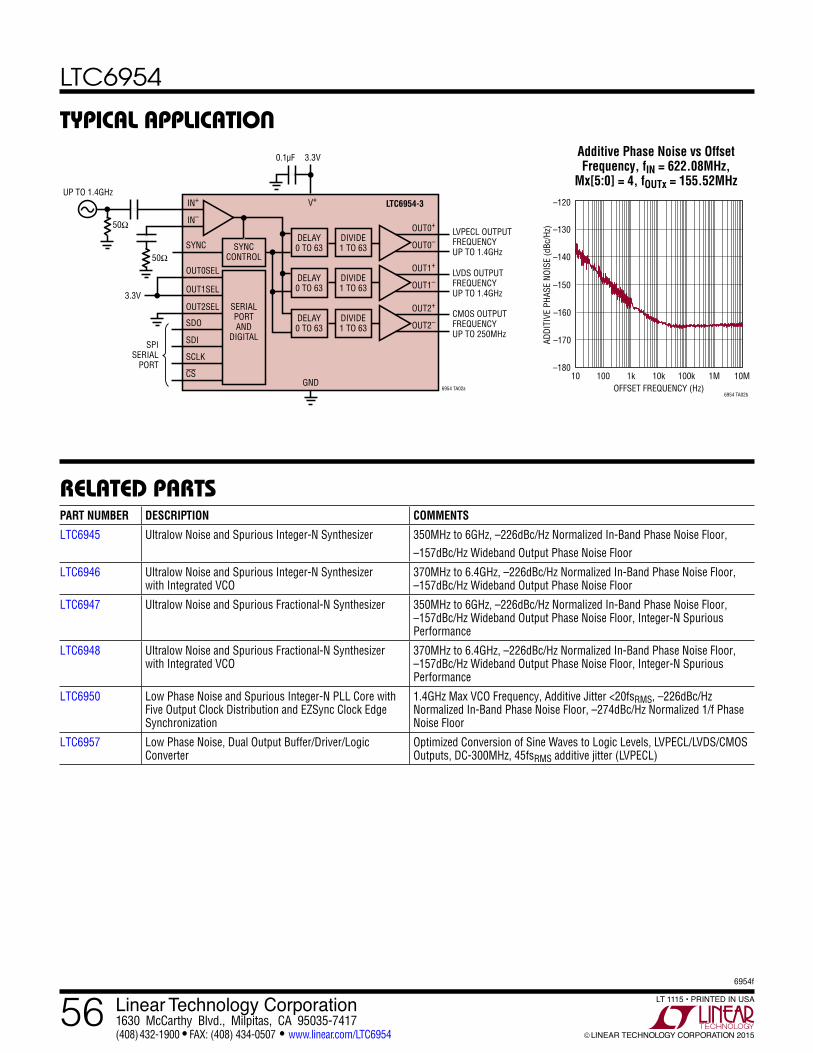
LTC6954
566954f
For more information www.linear.com/LTC6954 LINEAR TECHNOLOGY CORPORATION 2015
LT 1115 • PRINTED IN USALinear Technology Corporation1630 McCarthy Blvd., Milpitas, CA 95035-7417(408) 432-1900 FAX: (408) 434-0507 www.linear.com/LTC6954
relaTeD parTs
Typical applicaTion
PART NUMBER DESCRIPTION COMMENTS
LTC6945 Ultralow Noise and Spurious Integer-N Synthesizer 350MHz to 6GHz, –226dBc/Hz Normalized In-Band Phase Noise Floor,–157dBc/Hz Wideband Output Phase Noise Floor
LTC6946 Ultralow Noise and Spurious Integer-N Synthesizer with Integrated VCO
370MHz to 6.4GHz, –226dBc/Hz Normalized In-Band Phase Noise Floor, –157dBc/Hz Wideband Output Phase Noise Floor
LTC6947 Ultralow Noise and Spurious Fractional-N Synthesizer 350MHz to 6GHz, –226dBc/Hz Normalized In-Band Phase Noise Floor, –157dBc/Hz Wideband Output Phase Noise Floor, Integer-N Spurious Performance
LTC6948 Ultralow Noise and Spurious Fractional-N Synthesizer with Integrated VCO
370MHz to 6.4GHz, –226dBc/Hz Normalized In-Band Phase Noise Floor, –157dBc/Hz Wideband Output Phase Noise Floor, Integer-N Spurious Performance
LTC6950 Low Phase Noise and Spurious Integer-N PLL Core with Five Output Clock Distribution and EZSync Clock Edge Synchronization
1.4GHz Max VCO Frequency, Additive Jitter <20fsRMS, –226dBc/Hz Normalized In-Band Phase Noise Floor, –274dBc/Hz Normalized 1/f Phase Noise Floor
LTC6957 Low Phase Noise, Dual Output Buffer/Driver/Logic Converter
Optimized Conversion of Sine Waves to Logic Levels, LVPECL/LVDS/CMOS Outputs, DC-300MHz, 45fsRMS additive jitter (LVPECL)
Additive Phase Noise vs Offset Frequency, fIN = 622.08MHz,
Mx[5:0] = 4, fOUTx = 155.52MHz
6954 TA02a
LVPECL OUTPUTFREQUENCYUP TO 1.4GHz
LVDS OUTPUTFREQUENCYUP TO 1.4GHz
CMOS OUTPUTFREQUENCYUP TO 250MHz
OUT2+
OUT2–DIVIDE1 TO 63
DELAY0 TO 63
OUT1+
OUT1–DIVIDE1 TO 63
DELAY0 TO 63
OUT0+
OUT0–
SPISERIAL
PORT
DIVIDE1 TO 63
DELAY0 TO 63
V+
3.3V0.1µF
3.3V
SCLK
CSGND
SDO
SDI
OUT0SEL
OUT1SEL
OUT2SEL
SYNC
IN+
IN–
LTC6954-3UP TO 1.4GHz
50Ω
50ΩSYNC
CONTROL
SERIALPORTAND
DIGITAL
–180
ADDI
TIVE
PHA
SE N
OISE
(dBc
/Hz)
–160
–150
–130
–120
–170
–140
6954 TA02bOFFSET FREQUENCY (Hz)
10 100 1k 1M 10M100k10k