4 x 45 W power amplifier with full I2C diagnostics, high ... · 323 CKI2C bus clock/HE selector 4...
42
This is information on a product in full production. December 2014 DocID025599 Rev 6 1/42 TDA75610SLV 4 x 45 W power amplifier with full I 2 C diagnostics, high efficiency and low voltage operation Datasheet - production data Features Multipower BCD technology MOSFET output power stage DMOS power output High efficiency (class SB) High output power capability 4x25 W/4 Ω @ 14.4 V, 1 kHz, 10% THD, 4 x 45 W max power 2 Ω driving capability (64 W max power) Full I 2 C bus driving: – Standby – Independent front/rear soft play/mute – Selectable gain 26 dB /16 dB (for low noise line output function) – High efficiency enable/disable – I 2 C bus digital diagnostics (including DC and AC load detection) Flexible fault detection through integrated diagnostic DC offset detection Four independent short circuit protection Clipping detector pin with selectable threshold (2 %/10 %) Standby/mute pin Linear thermal shutdown with multiple thermal warning ESD protection Very robust against misconnections Improved SVR suppression during battery transients Capable to operate down to 6 V (e.g. “Start-stop”) Description The TDA75610SLV is a new quad bridge car radio amplifier, designed in BCD technology, in order to include a wide range of innovative features in a very compact and flexible device. The TDA75610SLV is equipped with the most complete diagnostics array that communicates the status of each speaker through the I 2 C bus. The dissipated output power under average listening condition is significantly reduced when compared to the conventional class AB solutions, thanks to the patented 'class SB' efficiency concept. TDA75610SLV has been designed to be very robust against several kinds of misconnections. It is moreover compliant to the most recent OEM specifications for low voltage operation (so called 'start-stop' battery profile during engine stop), helping car manufacturers to reduce the overall emissions and thus contributing to environment protection. The ST BCD in combination with 'class SB' efficiency and 'intelligent power' has been sold in million of units to most known car manufacturers, the TDA75610SLV is the latest and most compact member of this power amplifiers family. PowerSO36 Flexiwatt27 (Vert.) Flexiwatt27 (SMD) Flexiwatt27 (Horiz.) Table 1. Device summary Order code Package Packing TDA75610S-8ZX Flexiwatt27 (SMD) Tube TDA75610S-8ZT Tape and reel TDA75610S-48X Flexiwatt27 (vert.) Tube TDA75610S-QLX Flexiwatt27 (hor.) Tube TDA75610S-ZSX PowerSO36 Tube TDA75610S-ZST Tape and reel www.st.com
Transcript of 4 x 45 W power amplifier with full I2C diagnostics, high ... · 323 CKI2C bus clock/HE selector 4...
This is information on a product in full production.
December 2014 DocID025599 Rev 6 1/42
TDA75610SLV
4 x 45 W power amplifier with full I2C diagnostics, high efficiencyand low voltage operation
Datasheet - production data
Features
Multipower BCD technology
MOSFET output power stage
DMOS power output
High efficiency (class SB)
High output power capability 4x25 W/4 Ω @ 14.4 V, 1 kHz, 10% THD, 4 x 45 W max power
2 Ω driving capability (64 W max power)
Full I2C bus driving:
– Standby
– Independent front/rear soft play/mute
– Selectable gain 26 dB /16 dB (for low noise line output function)
– High efficiency enable/disable
– I2C bus digital diagnostics (including DC and AC load detection)
Flexible fault detection through integrated diagnostic
DC offset detection
Four independent short circuit protection
Clipping detector pin with selectable threshold (2 %/10 %)
Standby/mute pin
Linear thermal shutdown with multiple thermal warning
ESD protection
Very robust against misconnections
Improved SVR suppression during battery transients
Capable to operate down to 6 V (e.g. “Start-stop”)
Description
The TDA75610SLV is a new quad bridge car radio amplifier, designed in BCD technology, in order to include a wide range of innovative features in a very compact and flexible device.
The TDA75610SLV is equipped with the most complete diagnostics array that communicates the status of each speaker through the I2C bus.
The dissipated output power under average listening condition is significantly reduced when compared to the conventional class AB solutions, thanks to the patented 'class SB' efficiency concept. TDA75610SLV has been designed to be very robust against several kinds of misconnections. It is moreover compliant to the most recent OEM specifications for low voltage operation (so called 'start-stop' battery profile during engine stop), helping car manufacturers to reduce the overall emissions and thus contributing to environment protection. The ST BCD in combination with 'class SB' efficiency and 'intelligent power' has been sold in million of units to most known car manufacturers, the TDA75610SLV is the latest and most compact member of this power amplifiers family.
PowerSO36Flexiwatt27 (Vert.)
Flexiwatt27 (SMD)Flexiwatt27 (Horiz.)
Table 1. Device summary
Order code Package Packing
TDA75610S-8ZX Flexiwatt27 (SMD)
Tube
TDA75610S-8ZT Tape and reel
TDA75610S-48X Flexiwatt27 (vert.) Tube
TDA75610S-QLX Flexiwatt27 (hor.) Tube
TDA75610S-ZSXPowerSO36
Tube
TDA75610S-ZST Tape and reel
www.st.com
Contents TDA75610SLV
2/42 DocID025599 Rev 6
Contents
1 Block diagram and application circuits . . . . . . . . . . . . . . . . . . . . . . . . . 6
2 Pin description . . . . . . . . . . . . . . . . . . . . . . . . . . . . . . . . . . . . . . . . . . . . . 8
3 Electrical specifications . . . . . . . . . . . . . . . . . . . . . . . . . . . . . . . . . . . . . 10
3.1 Absolute maximum ratings . . . . . . . . . . . . . . . . . . . . . . . . . . . . . . . . . . . . 10
3.2 Thermal data . . . . . . . . . . . . . . . . . . . . . . . . . . . . . . . . . . . . . . . . . . . . . . 10
3.3 Electrical characteristics . . . . . . . . . . . . . . . . . . . . . . . . . . . . . . . . . . . . . . .11
3.4 Typical electrical characteristics curves . . . . . . . . . . . . . . . . . . . . . . . . . . 15
4 Diagnostics functional description . . . . . . . . . . . . . . . . . . . . . . . . . . . . 18
4.1 Turn-on diagnostic . . . . . . . . . . . . . . . . . . . . . . . . . . . . . . . . . . . . . . . . . . 18
4.2 Permanent diagnostics . . . . . . . . . . . . . . . . . . . . . . . . . . . . . . . . . . . . . . . 20
4.3 Output DC offset detection . . . . . . . . . . . . . . . . . . . . . . . . . . . . . . . . . . . . 21
4.4 AC diagnostic . . . . . . . . . . . . . . . . . . . . . . . . . . . . . . . . . . . . . . . . . . . . . . 21
5 Multiple faults . . . . . . . . . . . . . . . . . . . . . . . . . . . . . . . . . . . . . . . . . . . . . 23
5.1 Faults availability . . . . . . . . . . . . . . . . . . . . . . . . . . . . . . . . . . . . . . . . . . . 23
6 Thermal protection . . . . . . . . . . . . . . . . . . . . . . . . . . . . . . . . . . . . . . . . . 24
6.1 Fast muting . . . . . . . . . . . . . . . . . . . . . . . . . . . . . . . . . . . . . . . . . . . . . . . . 24
7 Battery transitions management . . . . . . . . . . . . . . . . . . . . . . . . . . . . . . 25
7.1 Low voltage operation (“start stop”) . . . . . . . . . . . . . . . . . . . . . . . . . . . . . 25
7.2 Advanced battery management . . . . . . . . . . . . . . . . . . . . . . . . . . . . . . . . 26
8 Application suggestion . . . . . . . . . . . . . . . . . . . . . . . . . . . . . . . . . . . . . . 27
8.1 Inputs impedance matching . . . . . . . . . . . . . . . . . . . . . . . . . . . . . . . . . . . 27
8.2 High efficiency introduction . . . . . . . . . . . . . . . . . . . . . . . . . . . . . . . . . . . 28
9 I2C bus . . . . . . . . . . . . . . . . . . . . . . . . . . . . . . . . . . . . . . . . . . . . . . . . . . . 29
9.1 I2C programming/reading sequences . . . . . . . . . . . . . . . . . . . . . . . . . . . . 29
9.2 Address selection and I2C disable . . . . . . . . . . . . . . . . . . . . . . . . . . . . . . 29
DocID025599 Rev 6 3/42
TDA75610SLV Contents
3
9.3 I2C bus interface . . . . . . . . . . . . . . . . . . . . . . . . . . . . . . . . . . . . . . . . . . . . 29
9.3.1 Data validity . . . . . . . . . . . . . . . . . . . . . . . . . . . . . . . . . . . . . . . . . . . . . . 29
9.3.2 Start and stop conditions . . . . . . . . . . . . . . . . . . . . . . . . . . . . . . . . . . . . 30
9.3.3 Byte format . . . . . . . . . . . . . . . . . . . . . . . . . . . . . . . . . . . . . . . . . . . . . . 30
9.3.4 Acknowledge . . . . . . . . . . . . . . . . . . . . . . . . . . . . . . . . . . . . . . . . . . . . . 30
10 Software specifications . . . . . . . . . . . . . . . . . . . . . . . . . . . . . . . . . . . . . 31
11 Examples of bytes sequence . . . . . . . . . . . . . . . . . . . . . . . . . . . . . . . . . 36
12 Package information . . . . . . . . . . . . . . . . . . . . . . . . . . . . . . . . . . . . . . . . 37
13 Revision history . . . . . . . . . . . . . . . . . . . . . . . . . . . . . . . . . . . . . . . . . . . 41
List of tables TDA75610SLV
4/42 DocID025599 Rev 6
List of tables
Table 1. Device summary . . . . . . . . . . . . . . . . . . . . . . . . . . . . . . . . . . . . . . . . . . . . . . . . . . . . . . . . . . 1Table 2. Pin list description. . . . . . . . . . . . . . . . . . . . . . . . . . . . . . . . . . . . . . . . . . . . . . . . . . . . . . . . . 9Table 3. Absolute maximum ratings . . . . . . . . . . . . . . . . . . . . . . . . . . . . . . . . . . . . . . . . . . . . . . . . . 10Table 4. Thermal data. . . . . . . . . . . . . . . . . . . . . . . . . . . . . . . . . . . . . . . . . . . . . . . . . . . . . . . . . . . . 10Table 5. Electrical characteristics . . . . . . . . . . . . . . . . . . . . . . . . . . . . . . . . . . . . . . . . . . . . . . . . . . . 11Table 6. Double fault table for turn on diagnostic . . . . . . . . . . . . . . . . . . . . . . . . . . . . . . . . . . . . . . . 23Table 7. IB1 . . . . . . . . . . . . . . . . . . . . . . . . . . . . . . . . . . . . . . . . . . . . . . . . . . . . . . . . . . . . . . . . . . . 31Table 8. IB2 . . . . . . . . . . . . . . . . . . . . . . . . . . . . . . . . . . . . . . . . . . . . . . . . . . . . . . . . . . . . . . . . . . . 32Table 9. DB1. . . . . . . . . . . . . . . . . . . . . . . . . . . . . . . . . . . . . . . . . . . . . . . . . . . . . . . . . . . . . . . . . . . 32Table 10. DB2. . . . . . . . . . . . . . . . . . . . . . . . . . . . . . . . . . . . . . . . . . . . . . . . . . . . . . . . . . . . . . . . . . . 33Table 11. DB3. . . . . . . . . . . . . . . . . . . . . . . . . . . . . . . . . . . . . . . . . . . . . . . . . . . . . . . . . . . . . . . . . . . 34Table 12. DB4. . . . . . . . . . . . . . . . . . . . . . . . . . . . . . . . . . . . . . . . . . . . . . . . . . . . . . . . . . . . . . . . . . . 35Table 13. Document revision history . . . . . . . . . . . . . . . . . . . . . . . . . . . . . . . . . . . . . . . . . . . . . . . . . 41
DocID025599 Rev 6 5/42
TDA75610SLV List of figures
5
List of figures
Figure 1. Block diagram . . . . . . . . . . . . . . . . . . . . . . . . . . . . . . . . . . . . . . . . . . . . . . . . . . . . . . . . . . . . 6Figure 2. Application circuit for Flexiwatt packages . . . . . . . . . . . . . . . . . . . . . . . . . . . . . . . . . . . . . . . 6Figure 3. Application circuit for PowerSO package . . . . . . . . . . . . . . . . . . . . . . . . . . . . . . . . . . . . . . . 7Figure 4. Pin connection diagram of the Flexiwatt27 (top of view) . . . . . . . . . . . . . . . . . . . . . . . . . . . 8Figure 5. Pin connection diagram of the PowerSO36 slug up (top of view). . . . . . . . . . . . . . . . . . . . . 8Figure 6. Quiescent current vs. supply voltage . . . . . . . . . . . . . . . . . . . . . . . . . . . . . . . . . . . . . . . . . 15Figure 7. Output power vs. supply voltage (4 Ω) . . . . . . . . . . . . . . . . . . . . . . . . . . . . . . . . . . . . . . . . 15Figure 8. Output power vs. supply voltage (2 Ω) . . . . . . . . . . . . . . . . . . . . . . . . . . . . . . . . . . . . . . . . 15Figure 9. Distortion vs. output power (4 Ω, STD) . . . . . . . . . . . . . . . . . . . . . . . . . . . . . . . . . . . . . . . . 15Figure 10. Distortion vs. output power (4 Ω, HI-EFF). . . . . . . . . . . . . . . . . . . . . . . . . . . . . . . . . . . . . . 15Figure 11. Distortion vs. output power (2 Ω, STD) . . . . . . . . . . . . . . . . . . . . . . . . . . . . . . . . . . . . . . . . 15Figure 12. Distortion vs. output power (2 Ω, HI-EFF). . . . . . . . . . . . . . . . . . . . . . . . . . . . . . . . . . . . . . 16Figure 13. Distortion vs. output power Vs = 6 V (4 Ω, STD). . . . . . . . . . . . . . . . . . . . . . . . . . . . . . . . . 16Figure 14. Distortion vs. frequency (4 Ω) . . . . . . . . . . . . . . . . . . . . . . . . . . . . . . . . . . . . . . . . . . . . . . . 16Figure 15. Distortion vs. frequency (2 Ω) . . . . . . . . . . . . . . . . . . . . . . . . . . . . . . . . . . . . . . . . . . . . . . . 16Figure 16. Crosstalk vs. frequency . . . . . . . . . . . . . . . . . . . . . . . . . . . . . . . . . . . . . . . . . . . . . . . . . . . 16Figure 17. Supply voltage rejection vs. frequency . . . . . . . . . . . . . . . . . . . . . . . . . . . . . . . . . . . . . . . . 16Figure 18. Power dissipation vs. average output power (audio program simulation, 4 Ω) . . . . . . . . . . 17Figure 19. Power dissipation vs. average output power (audio program simulation, 2 Ω) . . . . . . . . . . 17Figure 20. Total power dissipation and efficiency vs. output power (4 Ω, HI-EFF, Sine). . . . . . . . . . . 17Figure 21. Total power dissipation and efficiency vs. output power (4 Ω, STD, Sine) . . . . . . . . . . . . . 17Figure 22. ITU R-ARM frequency response, weighting filter for transient pop. . . . . . . . . . . . . . . . . . . 17Figure 23. Turn-on diagnostic: working principle . . . . . . . . . . . . . . . . . . . . . . . . . . . . . . . . . . . . . . . . . 18Figure 24. SVR and output behavior (Case 1: without turn-on diagnostic) . . . . . . . . . . . . . . . . . . . . . 18Figure 25. SVR and output pin behavior (Case 2: with turn-on diagnostic) . . . . . . . . . . . . . . . . . . . . . 19Figure 26. Short circuit detection thresholds . . . . . . . . . . . . . . . . . . . . . . . . . . . . . . . . . . . . . . . . . . . . 19Figure 27. Load detection thresholds - high gain setting . . . . . . . . . . . . . . . . . . . . . . . . . . . . . . . . . . . 19Figure 28. Load detection threshold - low gain setting . . . . . . . . . . . . . . . . . . . . . . . . . . . . . . . . . . . . 19Figure 29. Restart timing without diagnostic enable (permanent) - Each 1 mS time,
a sampling of the fault is done . . . . . . . . . . . . . . . . . . . . . . . . . . . . . . . . . . . . . . . . . . . . . . 20Figure 30. Restart timing with diagnostic enable (permanent). . . . . . . . . . . . . . . . . . . . . . . . . . . . . . . 20Figure 31. Current detection high: load impedance |Z| vs. output peak voltage . . . . . . . . . . . . . . . . . 22Figure 32. Current detection low: load impedance |Z| vs. output peak voltage . . . . . . . . . . . . . . . . . . 22Figure 33. Thermal foldback diagram . . . . . . . . . . . . . . . . . . . . . . . . . . . . . . . . . . . . . . . . . . . . . . . . . 24Figure 34. Worst case battery cranking curve sample 1 . . . . . . . . . . . . . . . . . . . . . . . . . . . . . . . . . . . 25Figure 35. Worst case battery cranking curve sample 2 . . . . . . . . . . . . . . . . . . . . . . . . . . . . . . . . . . . 25Figure 36. Upwards fast battery transitions diagram . . . . . . . . . . . . . . . . . . . . . . . . . . . . . . . . . . . . . . 26Figure 37. Inputs impedance matching circuit . . . . . . . . . . . . . . . . . . . . . . . . . . . . . . . . . . . . . . . . . . . 27Figure 38. High efficiency - basic structure . . . . . . . . . . . . . . . . . . . . . . . . . . . . . . . . . . . . . . . . . . . . . 28Figure 39. Data validity on the I2C bus . . . . . . . . . . . . . . . . . . . . . . . . . . . . . . . . . . . . . . . . . . . . . . . . 30Figure 40. Timing diagram on the I2C bus . . . . . . . . . . . . . . . . . . . . . . . . . . . . . . . . . . . . . . . . . . . . . . 30Figure 41. Acknowledge on the I2C bus . . . . . . . . . . . . . . . . . . . . . . . . . . . . . . . . . . . . . . . . . . . . . . . 30Figure 42. Flexiwatt27 (horizontal) mechanical data and package dimensions. . . . . . . . . . . . . . . . . . 37Figure 43. Flexiwatt27 (vertical) mechanical data and package dimensions. . . . . . . . . . . . . . . . . . . . 38Figure 44. Flexiwatt27 (SMD) mechanical data and package dimensions . . . . . . . . . . . . . . . . . . . . . 39Figure 45. PowerSO36 (slug up) mechanical data and package dimensions . . . . . . . . . . . . . . . . . . . 40
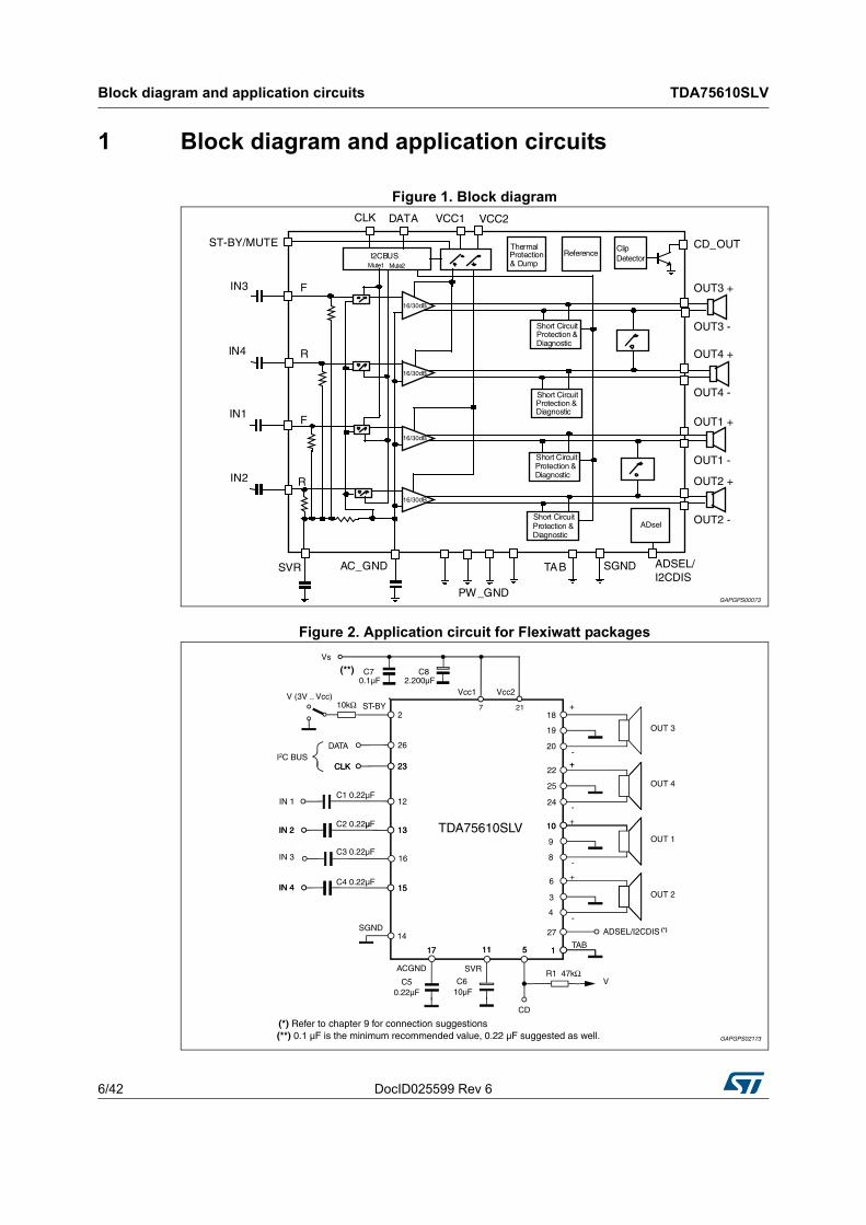
Block diagram and application circuits TDA75610SLV
6/42 DocID025599 Rev 6
1 Block diagram and application circuits
Figure 1. Block diagram
Figure 2. Application circuit for Flexiwatt packages
DocID025599 Rev 6 7/42
TDA75610SLV Block diagram and application circuits
41
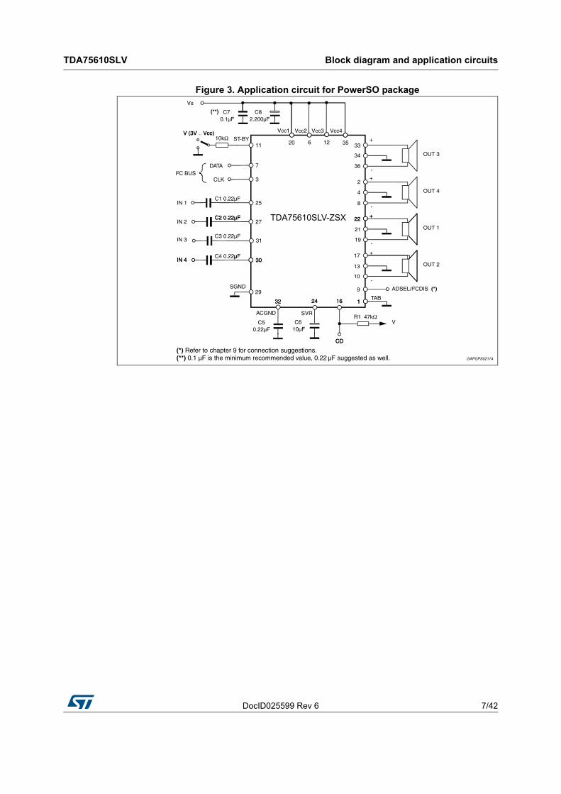
Figure 3. Application circuit for PowerSO package
Pin description TDA75610SLV
8/42 DocID025599 Rev 6
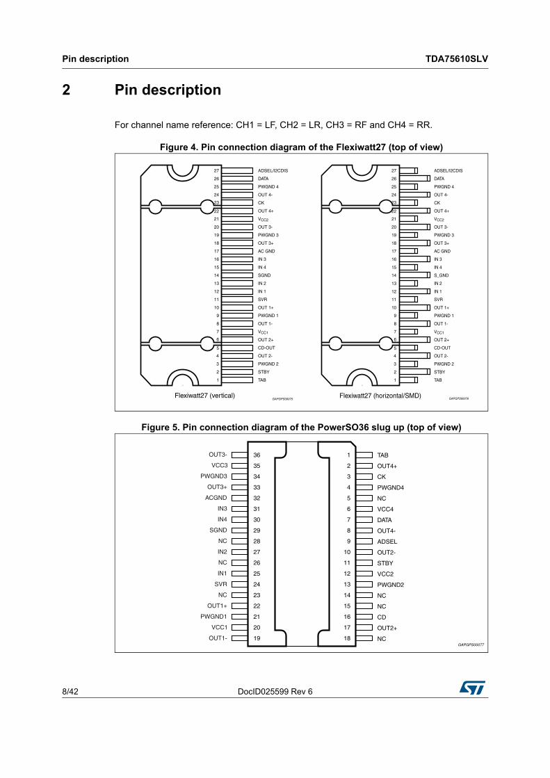
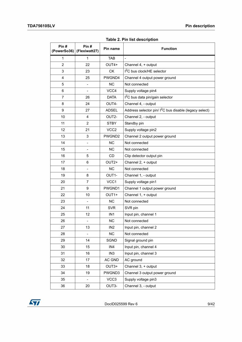
2 Pin description
For channel name reference: CH1 = LF, CH2 = LR, CH3 = RF and CH4 = RR.
Figure 4. Pin connection diagram of the Flexiwatt27 (top of view)
Figure 5. Pin connection diagram of the PowerSO36 slug up (top of view)
DocID025599 Rev 6 9/42
TDA75610SLV Pin description
41
Table 2. Pin list description
Pin # (PowerSo36)
Pin # (Flexiwatt27)
Pin name Function
1 1 TAB -
2 22 OUT4+ Channel 4, + output
3 23 CK I2C bus clock/HE selector
4 25 PWGND4 Channel 4 output power ground
5 - NC Not connected
6 - VCC4 Supply voltage pin4
7 26 DATA I2C bus data pin/gain selector
8 24 OUT4- Channel 4, - output
9 27 ADSEL Address selector pin/ I2C bus disable (legacy select)
10 4 OUT2- Channel 2, - output
11 2 STBY Standby pin
12 21 VCC2 Supply voltage pin2
13 3 PWGND2 Channel 2 output power ground
14 - NC Not connected
15 - NC Not connected
16 5 CD Clip detector output pin
17 6 OUT2+ Channel 2, + output
18 - NC Not connected
19 8 OUT1- Channel 1, - output
20 7 VCC1 Supply voltage pin1
21 9 PWGND1 Channel 1 output power ground
22 10 OUT1+ Channel 1, + output
23 - NC Not connected
24 11 SVR SVR pin
25 12 IN1 Input pin, channel 1
26 - NC Not connected
27 13 IN2 Input pin, channel 2
28 - NC Not connected
29 14 SGND Signal ground pin
30 15 IN4 Input pin, channel 4
31 16 IN3 Input pin, channel 3
32 17 AC GND AC ground
33 18 OUT3+ Channel 3, + output
34 19 PWGND3 Channel 3 output power ground
35 - VCC3 Supply voltage pin3
36 20 OUT3- Channel 3, - output
Electrical specifications TDA75610SLV
10/42 DocID025599 Rev 6
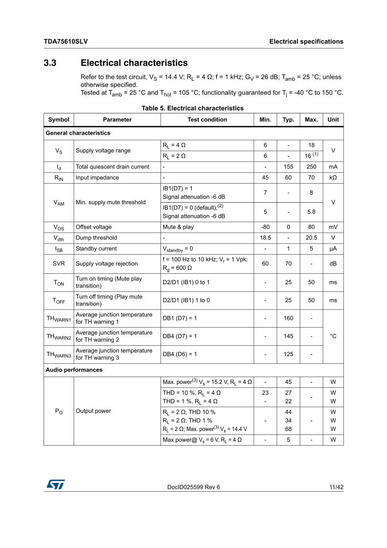
3 Electrical specifications
3.1 Absolute maximum ratings
3.2 Thermal data
Table 3. Absolute maximum ratings
Symbol Parameter Value Unit
Vop Operating supply voltage(1)
1. For RL = 2 Ω the output current limit might be reached for VOP > 16 V; thus triggering self-protection.
18 V
VS DC supply voltage 28 V
Vpeak Peak supply voltage (for tmax = 50 ms) 50 V
GNDmax Ground pins voltage -0.3 to 0.3 V
VCK, VDATA CK and DATA pin voltage -0.3 to 6 V
Vcd Clip detector voltage -0.3 to Vop V
Vstby STBY pin voltage -0.3 to Vop V
IOOutput peak current (not repetitive tmax = 100ms) 8
AOutput peak current (repetitive f > 10 kHz) 6
Ptot Power dissipation Tcase = 70°C 85 W
Tstg, Tj Storage and junction temperature(2)
2. A suitable dissipation system should be used to keep Tj inside the specified limits.
-55 to 150 °C
Tamb Operative temperature range -40 to 105 °C
Table 4. Thermal data
Symbol Parameter PowerSO Flexiwatt Unit
Rth j-case Thermal resistance junction-to-case Max. 1 1 °C/W
DocID025599 Rev 6 11/42
TDA75610SLV Electrical specifications
41
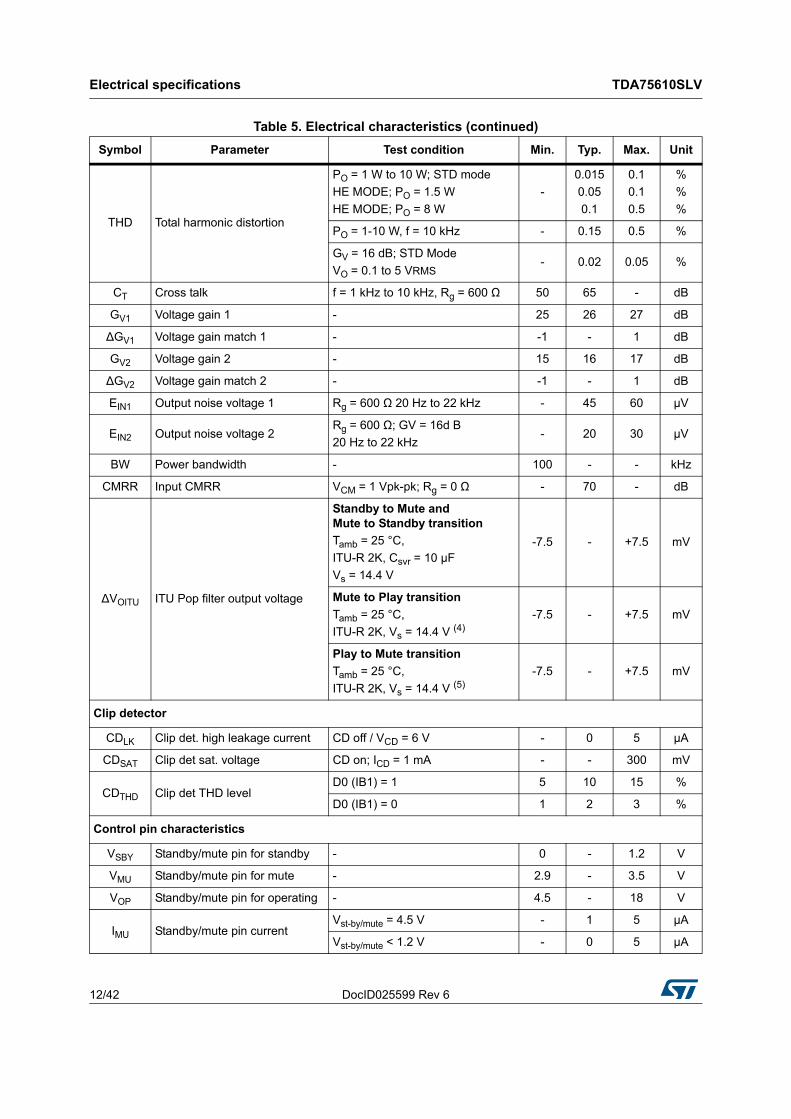
3.3 Electrical characteristicsRefer to the test circuit, VS = 14.4 V; RL = 4 Ω; f = 1 kHz; GV = 26 dB; Tamb = 25 °C; unless otherwise specified.Tested at Tamb = 25 °C and Thot = 105 °C; functionality guaranteed for Tj = -40 °C to 150 °C.
Table 5. Electrical characteristics
Symbol Parameter Test condition Min. Typ. Max. Unit
General characteristics
VS Supply voltage rangeRL = 4 Ω 6 - 18
VRL = 2 Ω 6 - 16 (1)
Id Total quiescent drain current - - 155 250 mA
RIN Input impedance - 45 60 70 kΩ
VAM Min. supply mute threshold
IB1(D7) = 1
Signal attenuation -6 dB7 - 8
VIB1(D7) = 0 (default);(2)
Signal attenuation -6 dB5 - 5.8
VOS Offset voltage Mute & play -80 0 80 mV
Vdth Dump threshold - 18.5 - 20.5 V
ISB Standby current Vstandby = 0 - 1 5 µA
SVR Supply voltage rejectionf = 100 Hz to 10 kHz; Vr = 1 Vpk;
Rg = 600 Ω60 70 - dB
TONTurn on timing (Mute play transition)
D2/D1 (IB1) 0 to 1 - 25 50 ms
TOFFTurn off timing (Play mute transition)
D2/D1 (IB1) 1 to 0 - 25 50 ms
THWARN1Average junction temperature for TH warning 1
DB1 (D7) = 1 - 160 -
°CTHWARN2Average junction temperature for TH warning 2
DB4 (D7) = 1 - 145 -
THWARN3Average junction temperature for TH warning 3
DB4 (D6) = 1 - 125 -
Audio performances
PO Output power
Max. power(3) Vs = 15.2 V, RL = 4 Ω - 45 - W
THD = 10 %, RL = 4 Ω
THD = 1 %, RL = 4 Ω
23
-
27
22-
W
W
RL = 2 Ω; THD 10 %
RL = 2 Ω; THD 1 %
RL = 2 Ω; Max. power(3) Vs = 14.4 V
-
44
34
68
-
W
W
W
Max power@ Vs = 6 V, RL = 4 Ω - 5 - W
Electrical specifications TDA75610SLV
12/42 DocID025599 Rev 6
THD Total harmonic distortion
PO = 1 W to 10 W; STD mode
HE MODE; PO = 1.5 W
HE MODE; PO = 8 W
-
0.015
0.05
0.1
0.1
0.1
0.5
%
%
%
PO = 1-10 W, f = 10 kHz - 0.15 0.5 %
GV = 16 dB; STD Mode
VO = 0.1 to 5 VRMS- 0.02 0.05 %
CT Cross talk f = 1 kHz to 10 kHz, Rg = 600 Ω 50 65 - dB
GV1 Voltage gain 1 - 25 26 27 dB
ΔGV1 Voltage gain match 1 - -1 - 1 dB
GV2 Voltage gain 2 - 15 16 17 dB
ΔGV2 Voltage gain match 2 - -1 - 1 dB
EIN1 Output noise voltage 1 Rg = 600 Ω 20 Hz to 22 kHz - 45 60 µV
EIN2 Output noise voltage 2Rg = 600 Ω; GV = 16d B
20 Hz to 22 kHz- 20 30 µV
BW Power bandwidth - 100 - - kHz
CMRR Input CMRR VCM = 1 Vpk-pk; Rg = 0 Ω - 70 - dB
ΔVOITU ITU Pop filter output voltage
Standby to Mute andMute to Standby transition
Tamb = 25 °C,
ITU-R 2K, Csvr = 10 µF
Vs = 14.4 V
-7.5 - +7.5 mV
Mute to Play transition
Tamb = 25 °C,
ITU-R 2K, Vs = 14.4 V (4)-7.5 - +7.5 mV
Play to Mute transition
Tamb = 25 °C,
ITU-R 2K, Vs = 14.4 V (5)-7.5 - +7.5 mV
Clip detector
CDLK Clip det. high leakage current CD off / VCD = 6 V - 0 5 µA
CDSAT Clip det sat. voltage CD on; ICD = 1 mA - - 300 mV
CDTHD Clip det THD levelD0 (IB1) = 1 5 10 15 %
D0 (IB1) = 0 1 2 3 %
Control pin characteristics
VSBY Standby/mute pin for standby - 0 - 1.2 V
VMU Standby/mute pin for mute - 2.9 - 3.5 V
VOP Standby/mute pin for operating - 4.5 - 18 V
IMU Standby/mute pin currentVst-by/mute = 4.5 V - 1 5 µA
Vst-by/mute < 1.2 V - 0 5 µA
Table 5. Electrical characteristics (continued)
Symbol Parameter Test condition Min. Typ. Max. Unit
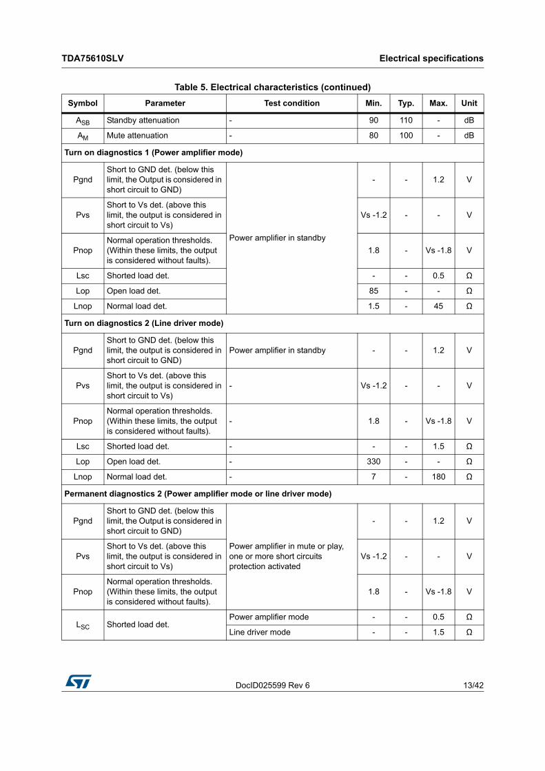
DocID025599 Rev 6 13/42
TDA75610SLV Electrical specifications
41
ASB Standby attenuation - 90 110 - dB
AM Mute attenuation - 80 100 - dB
Turn on diagnostics 1 (Power amplifier mode)
PgndShort to GND det. (below this limit, the Output is considered in short circuit to GND)
Power amplifier in standby
- - 1.2 V
PvsShort to Vs det. (above this limit, the output is considered in short circuit to Vs)
Vs -1.2 - - V
PnopNormal operation thresholds. (Within these limits, the output is considered without faults).
1.8 - Vs -1.8 V
Lsc Shorted load det. - - 0.5 Ω
Lop Open load det. 85 - - Ω
Lnop Normal load det. 1.5 - 45 Ω
Turn on diagnostics 2 (Line driver mode)
PgndShort to GND det. (below this limit, the output is considered in short circuit to GND)
Power amplifier in standby - - 1.2 V
PvsShort to Vs det. (above this limit, the output is considered in short circuit to Vs)
- Vs -1.2 - - V
PnopNormal operation thresholds. (Within these limits, the output is considered without faults).
- 1.8 - Vs -1.8 V
Lsc Shorted load det. - - - 1.5 Ω
Lop Open load det. - 330 - - Ω
Lnop Normal load det. - 7 - 180 Ω
Permanent diagnostics 2 (Power amplifier mode or line driver mode)
PgndShort to GND det. (below this limit, the Output is considered in short circuit to GND)
Power amplifier in mute or play, one or more short circuits protection activated
- - 1.2 V
PvsShort to Vs det. (above this limit, the output is considered in short circuit to Vs)
Vs -1.2 - - V
PnopNormal operation thresholds. (Within these limits, the output is considered without faults).
1.8 - Vs -1.8 V
LSC Shorted load det.Power amplifier mode - - 0.5 Ω
Line driver mode - - 1.5 Ω
Table 5. Electrical characteristics (continued)
Symbol Parameter Test condition Min. Typ. Max. Unit
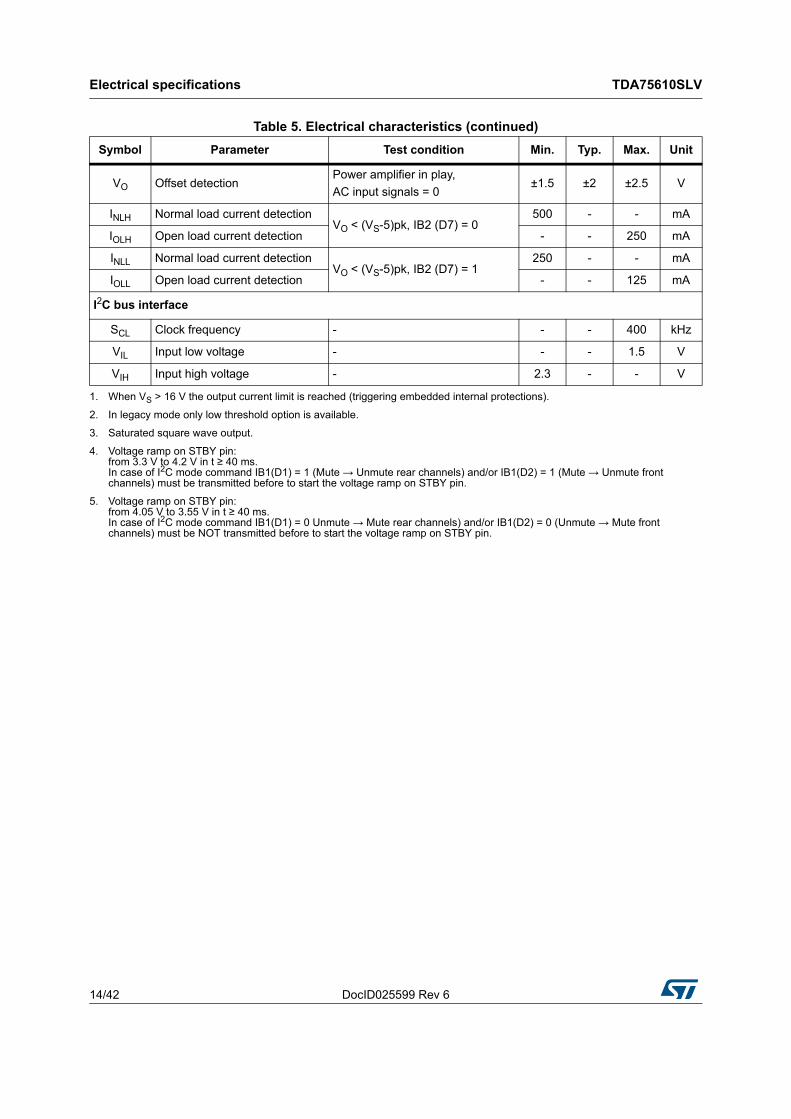
Electrical specifications TDA75610SLV
14/42 DocID025599 Rev 6
VO Offset detectionPower amplifier in play,
AC input signals = 0±1.5 ±2 ±2.5 V
INLH Normal load current detectionVO < (VS-5)pk, IB2 (D7) = 0
500 - - mA
IOLH Open load current detection - - 250 mA
INLL Normal load current detectionVO < (VS-5)pk, IB2 (D7) = 1
250 - - mA
IOLL Open load current detection - - 125 mA
I2C bus interface
SCL Clock frequency - - - 400 kHz
VIL Input low voltage - - - 1.5 V
VIH Input high voltage - 2.3 - - V
1. When VS > 16 V the output current limit is reached (triggering embedded internal protections).
2. In legacy mode only low threshold option is available.
3. Saturated square wave output.
4. Voltage ramp on STBY pin:from 3.3 V to 4.2 V in t ≥ 40 ms.In case of I2C mode command IB1(D1) = 1 (Mute → Unmute rear channels) and/or IB1(D2) = 1 (Mute → Unmute front channels) must be transmitted before to start the voltage ramp on STBY pin.
5. Voltage ramp on STBY pin:from 4.05 V to 3.55 V in t ≥ 40 ms.In case of I2C mode command IB1(D1) = 0 Unmute → Mute rear channels) and/or IB1(D2) = 0 (Unmute → Mute front channels) must be NOT transmitted before to start the voltage ramp on STBY pin.
Table 5. Electrical characteristics (continued)
Symbol Parameter Test condition Min. Typ. Max. Unit
DocID025599 Rev 6 15/42
TDA75610SLV Electrical specifications
41
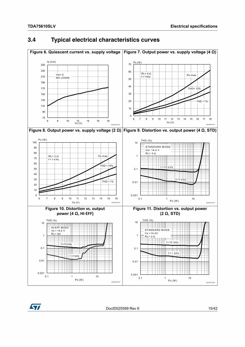
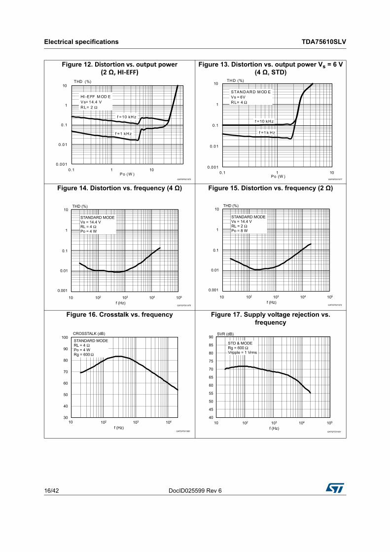
3.4 Typical electrical characteristics curves
Figure 6. Quiescent current vs. supply voltage Figure 7. Output power vs. supply voltage (4 Ω)
Figure 8. Output power vs. supply voltage (2 Ω) Figure 9. Distortion vs. output power (4 Ω, STD)
Figure 10. Distortion vs. output power (4 Ω, HI‐EFF)
Figure 11. Distortion vs. output power (2 Ω, STD)
Electrical specifications TDA75610SLV
16/42 DocID025599 Rev 6
Figure 12. Distortion vs. output power (2 Ω, HI‐EFF)
Figure 13. Distortion vs. output power Vs = 6 V (4 Ω, STD)
Figure 14. Distortion vs. frequency (4 Ω) Figure 15. Distortion vs. frequency (2 Ω)
Figure 16. Crosstalk vs. frequency Figure 17. Supply voltage rejection vs. frequency
DocID025599 Rev 6 17/42
TDA75610SLV Electrical specifications
41
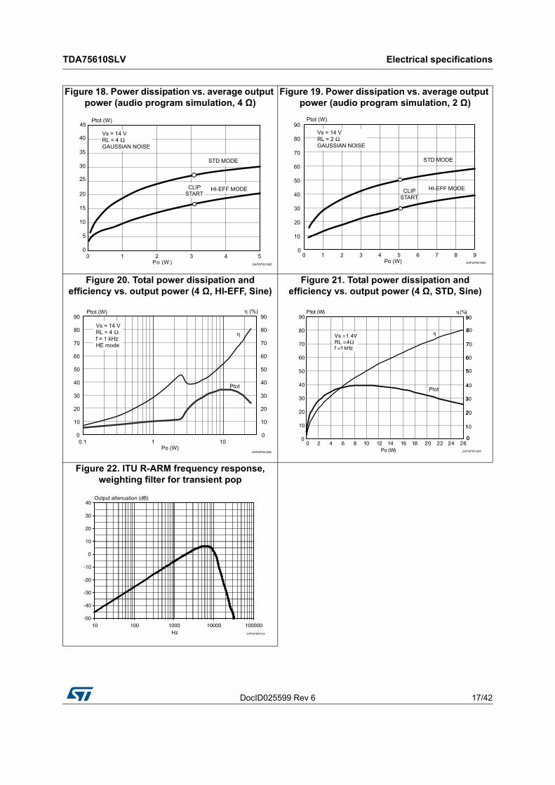
Figure 18. Power dissipation vs. average output power (audio program simulation, 4 Ω)
Figure 19. Power dissipation vs. average output power (audio program simulation, 2 Ω)
Figure 20. Total power dissipation and efficiency vs. output power (4 Ω, HI-EFF, Sine)
Figure 21. Total power dissipation and efficiency vs. output power (4 Ω, STD, Sine)
Figure 22. ITU R-ARM frequency response, weighting filter for transient pop
Diagnostics functional description TDA75610SLV
18/42 DocID025599 Rev 6
4 Diagnostics functional description
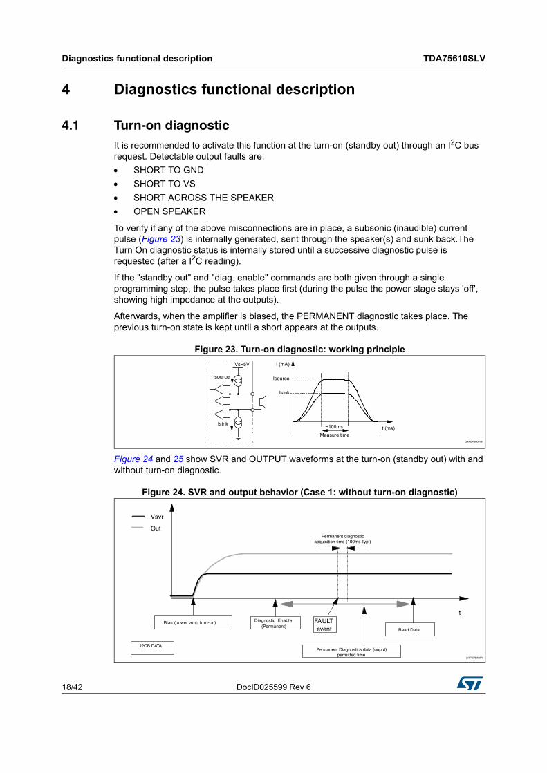
4.1 Turn-on diagnosticIt is recommended to activate this function at the turn-on (standby out) through an I2C bus request. Detectable output faults are:
SHORT TO GND
SHORT TO VS
SHORT ACROSS THE SPEAKER
OPEN SPEAKER
To verify if any of the above misconnections are in place, a subsonic (inaudible) current pulse (Figure 23) is internally generated, sent through the speaker(s) and sunk back.The Turn On diagnostic status is internally stored until a successive diagnostic pulse is requested (after a I2C reading).
If the "standby out" and "diag. enable" commands are both given through a single programming step, the pulse takes place first (during the pulse the power stage stays 'off', showing high impedance at the outputs).
Afterwards, when the amplifier is biased, the PERMANENT diagnostic takes place. The previous turn-on state is kept until a short appears at the outputs.
Figure 23. Turn-on diagnostic: working principle
Figure 24 and 25 show SVR and OUTPUT waveforms at the turn-on (standby out) with and without turn-on diagnostic.
Figure 24. SVR and output behavior (Case 1: without turn-on diagnostic)
DocID025599 Rev 6 19/42
TDA75610SLV Diagnostics functional description
41
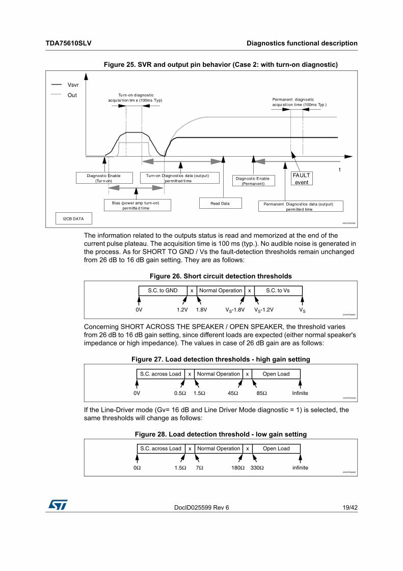
Figure 25. SVR and output pin behavior (Case 2: with turn-on diagnostic)
The information related to the outputs status is read and memorized at the end of the current pulse plateau. The acquisition time is 100 ms (typ.). No audible noise is generated in the process. As for SHORT TO GND / Vs the fault-detection thresholds remain unchanged from 26 dB to 16 dB gain setting. They are as follows:
Figure 26. Short circuit detection thresholds
Concerning SHORT ACROSS THE SPEAKER / OPEN SPEAKER, the threshold varies from 26 dB to 16 dB gain setting, since different loads are expected (either normal speaker's impedance or high impedance). The values in case of 26 dB gain are as follows:
Figure 27. Load detection thresholds - high gain setting
If the Line-Driver mode (Gv= 16 dB and Line Driver Mode diagnostic = 1) is selected, the same thresholds will change as follows:
Figure 28. Load detection threshold - low gain setting
Diagnostics functional description TDA75610SLV
20/42 DocID025599 Rev 6
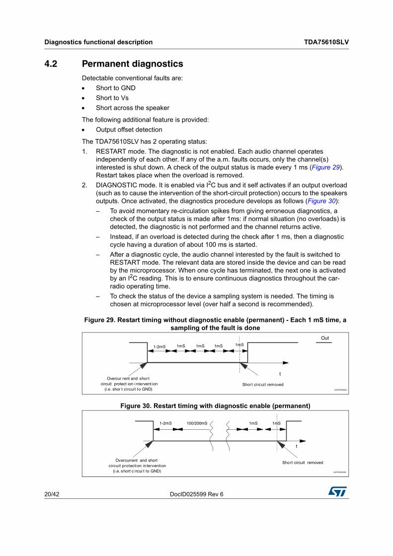
4.2 Permanent diagnosticsDetectable conventional faults are:
Short to GND
Short to Vs
Short across the speaker
The following additional feature is provided:
Output offset detection
The TDA75610SLV has 2 operating status:
1. RESTART mode. The diagnostic is not enabled. Each audio channel operates independently of each other. If any of the a.m. faults occurs, only the channel(s) interested is shut down. A check of the output status is made every 1 ms (Figure 29). Restart takes place when the overload is removed.
2. DIAGNOSTIC mode. It is enabled via I2C bus and it self activates if an output overload (such as to cause the intervention of the short-circuit protection) occurs to the speakers outputs. Once activated, the diagnostics procedure develops as follows (Figure 30):
– To avoid momentary re-circulation spikes from giving erroneous diagnostics, a check of the output status is made after 1ms: if normal situation (no overloads) is detected, the diagnostic is not performed and the channel returns active.
– Instead, if an overload is detected during the check after 1 ms, then a diagnostic cycle having a duration of about 100 ms is started.
– After a diagnostic cycle, the audio channel interested by the fault is switched to RESTART mode. The relevant data are stored inside the device and can be read by the microprocessor. When one cycle has terminated, the next one is activated by an I2C reading. This is to ensure continuous diagnostics throughout the car-radio operating time.
– To check the status of the device a sampling system is needed. The timing is chosen at microprocessor level (over half a second is recommended).
Figure 29. Restart timing without diagnostic enable (permanent) - Each 1 mS time, a sampling of the fault is done
Figure 30. Restart timing with diagnostic enable (permanent)
DocID025599 Rev 6 21/42
TDA75610SLV Diagnostics functional description
41
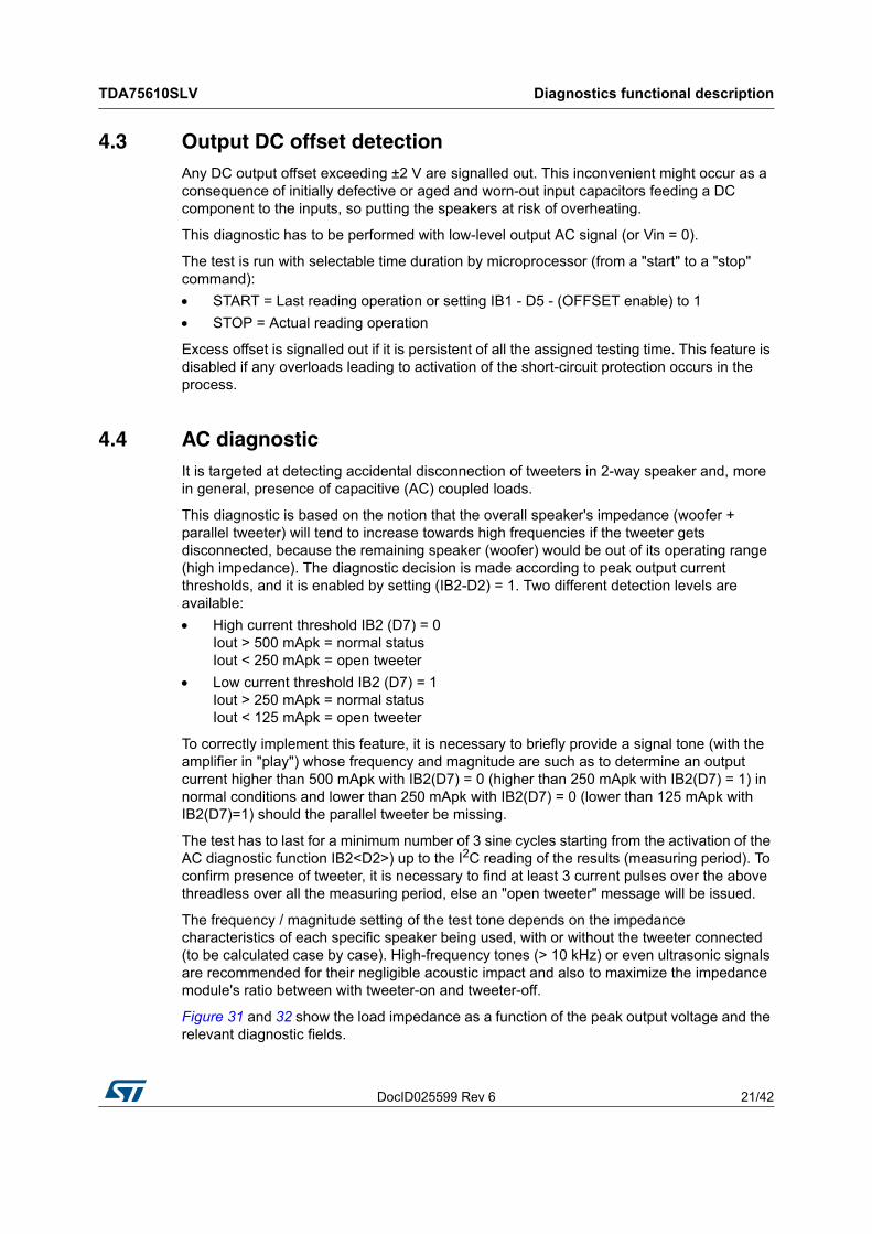
4.3 Output DC offset detectionAny DC output offset exceeding ±2 V are signalled out. This inconvenient might occur as a consequence of initially defective or aged and worn-out input capacitors feeding a DC component to the inputs, so putting the speakers at risk of overheating.
This diagnostic has to be performed with low-level output AC signal (or Vin = 0).
The test is run with selectable time duration by microprocessor (from a "start" to a "stop" command):
START = Last reading operation or setting IB1 - D5 - (OFFSET enable) to 1
STOP = Actual reading operation
Excess offset is signalled out if it is persistent of all the assigned testing time. This feature is disabled if any overloads leading to activation of the short-circuit protection occurs in the process.
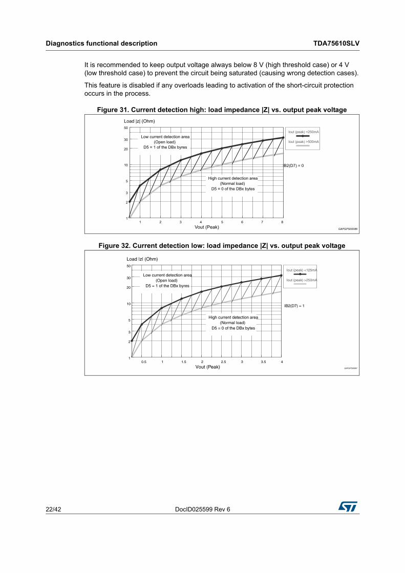
4.4 AC diagnosticIt is targeted at detecting accidental disconnection of tweeters in 2-way speaker and, more in general, presence of capacitive (AC) coupled loads.
This diagnostic is based on the notion that the overall speaker's impedance (woofer + parallel tweeter) will tend to increase towards high frequencies if the tweeter gets disconnected, because the remaining speaker (woofer) would be out of its operating range (high impedance). The diagnostic decision is made according to peak output current thresholds, and it is enabled by setting (IB2-D2) = 1. Two different detection levels are available:
High current threshold IB2 (D7) = 0Iout > 500 mApk = normal statusIout < 250 mApk = open tweeter
Low current threshold IB2 (D7) = 1Iout > 250 mApk = normal statusIout < 125 mApk = open tweeter
To correctly implement this feature, it is necessary to briefly provide a signal tone (with the amplifier in "play") whose frequency and magnitude are such as to determine an output current higher than 500 mApk with IB2(D7) = 0 (higher than 250 mApk with IB2(D7) = 1) in normal conditions and lower than 250 mApk with IB2(D7) = 0 (lower than 125 mApk with IB2(D7)=1) should the parallel tweeter be missing.
The test has to last for a minimum number of 3 sine cycles starting from the activation of the AC diagnostic function IB2<D2>) up to the I2C reading of the results (measuring period). To confirm presence of tweeter, it is necessary to find at least 3 current pulses over the above threadless over all the measuring period, else an "open tweeter" message will be issued.
The frequency / magnitude setting of the test tone depends on the impedance characteristics of each specific speaker being used, with or without the tweeter connected (to be calculated case by case). High-frequency tones (> 10 kHz) or even ultrasonic signals are recommended for their negligible acoustic impact and also to maximize the impedance module's ratio between with tweeter-on and tweeter-off.
Figure 31 and 32 show the load impedance as a function of the peak output voltage and the relevant diagnostic fields.
Diagnostics functional description TDA75610SLV
22/42 DocID025599 Rev 6
It is recommended to keep output voltage always below 8 V (high threshold case) or 4 V (low threshold case) to prevent the circuit being saturated (causing wrong detection cases).
This feature is disabled if any overloads leading to activation of the short-circuit protection occurs in the process.
Figure 31. Current detection high: load impedance |Z| vs. output peak voltage
Figure 32. Current detection low: load impedance |Z| vs. output peak voltage
DocID025599 Rev 6 23/42
TDA75610SLV Multiple faults
41
5 Multiple faults
When more misconnections are simultaneously in place at the audio outputs, it is guaranteed that at least one of them is initially read out. The others are notified after successive cycles of I2C reading and faults removal, provided that the diagnostic is enabled. This is true for both kinds of diagnostic (Turn on and Permanent).
The table below shows all the couples of double-fault possible. It should be taken into account that a short circuit with the 4 ohm speaker unconnected is considered as double fault.
In Permanent Diagnostic the table is the same, with only a difference concerning Open Load(*), which is not among the recognizable faults. Should an Open Load be present during the device's normal working, it would be detected at a subsequent Turn on Diagnostic cycle (i.e. at the successive Car Radio Turn on).
5.1 Faults availabilityAll the results coming from I2C bus, by read operations, are the consequence of measurements inside a defined period of time. If the fault is stable throughout the whole period, it will be sent out.
To guarantee always resident functions, every kind of diagnostic cycles (Turn on, Permanent, Offset) will be reactivate after any I2C reading operation. So, when the micro reads the I2C, a new cycle will be able to start, but the read data will come from the previous diag. cycle (i.e. The device is in Turn On state, with a short to Gnd, then the short is removed and micro reads I2C. The short to Gnd is still present in bytes, because it is the result of the previous cycle. If another I2C reading operation occurs, the bytes do not show the short). In general to observe a change in Diagnostic bytes, two I2C reading operations are necessary.
Table 6. Double fault table for turn on diagnostic
S. GND S. Vs S. Across L. Open L.
S. GND S. GND S. Vs + S. GND S. GND S. GND
S. Vs / S. Vs S. Vs S. Vs
S. Across L. / / S. Across L. N.A.
Open L. / / / Open L. (*)
Thermal protection TDA75610SLV
24/42 DocID025599 Rev 6
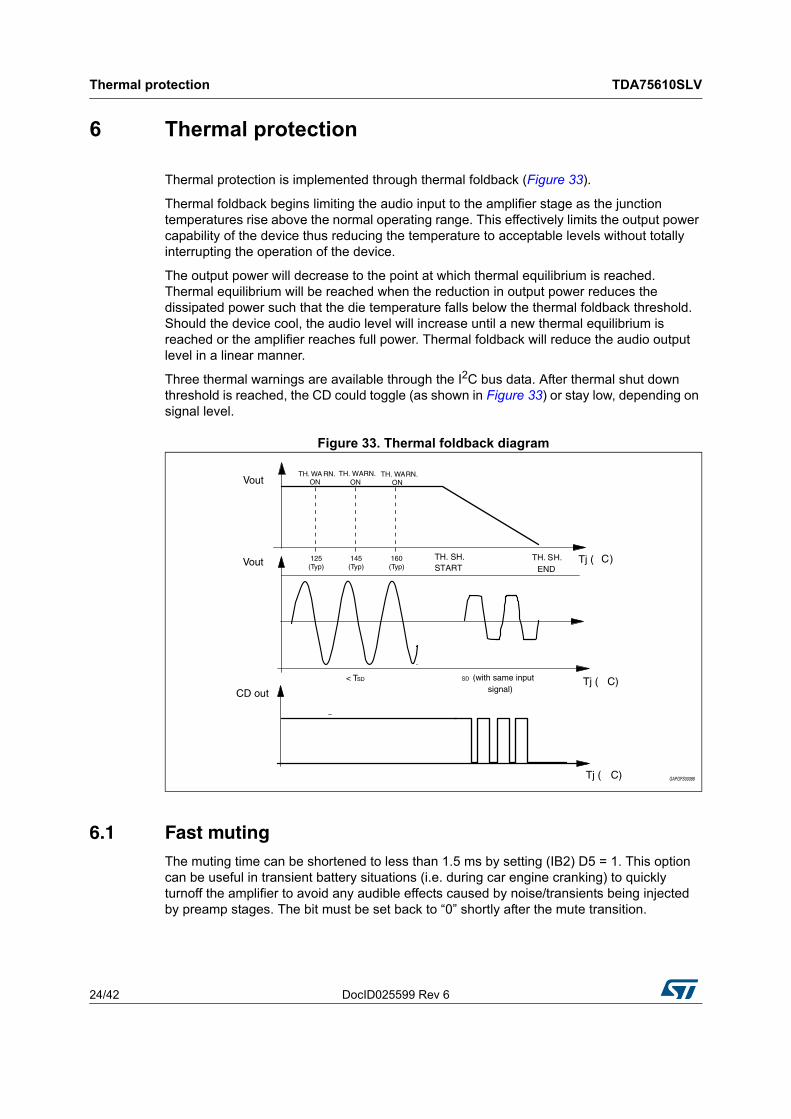
6 Thermal protection
Thermal protection is implemented through thermal foldback (Figure 33).
Thermal foldback begins limiting the audio input to the amplifier stage as the junction temperatures rise above the normal operating range. This effectively limits the output power capability of the device thus reducing the temperature to acceptable levels without totally interrupting the operation of the device.
The output power will decrease to the point at which thermal equilibrium is reached. Thermal equilibrium will be reached when the reduction in output power reduces the dissipated power such that the die temperature falls below the thermal foldback threshold. Should the device cool, the audio level will increase until a new thermal equilibrium is reached or the amplifier reaches full power. Thermal foldback will reduce the audio output level in a linear manner.
Three thermal warnings are available through the I2C bus data. After thermal shut down threshold is reached, the CD could toggle (as shown in Figure 33) or stay low, depending on signal level.
Figure 33. Thermal foldback diagram
6.1 Fast mutingThe muting time can be shortened to less than 1.5 ms by setting (IB2) D5 = 1. This option can be useful in transient battery situations (i.e. during car engine cranking) to quickly turnoff the amplifier to avoid any audible effects caused by noise/transients being injected by preamp stages. The bit must be set back to “0” shortly after the mute transition.
DocID025599 Rev 6 25/42
TDA75610SLV Battery transitions management
41
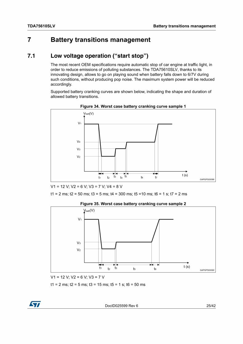
7 Battery transitions management
7.1 Low voltage operation (“start stop”)The most recent OEM specifications require automatic stop of car engine at traffic light, in order to reduce emissions of polluting substances. The TDA75610SLV, thanks to its innovating design, allows to go on playing sound when battery falls down to 6/7V during such conditions, without producing pop noise. The maximum system power will be reduced accordingly.
Supported battery cranking curves are shown below, indicating the shape and duration of allowed battery transitions.
Figure 34. Worst case battery cranking curve sample 1
V1 = 12 V; V2 = 6 V; V3 = 7 V; V4 = 8 V
t1 = 2 ms; t2 = 50 ms; t3 = 5 ms; t4 = 300 ms; t5 =10 ms; t6 = 1 s; t7 = 2 ms
Figure 35. Worst case battery cranking curve sample 2
V1 = 12 V; V2 = 6 V; V3 = 7 V
t1 = 2 ms; t2 = 5 ms; t3 = 15 ms; t5 = 1 s; t6 = 50 ms
Battery transitions management TDA75610SLV
26/42 DocID025599 Rev 6
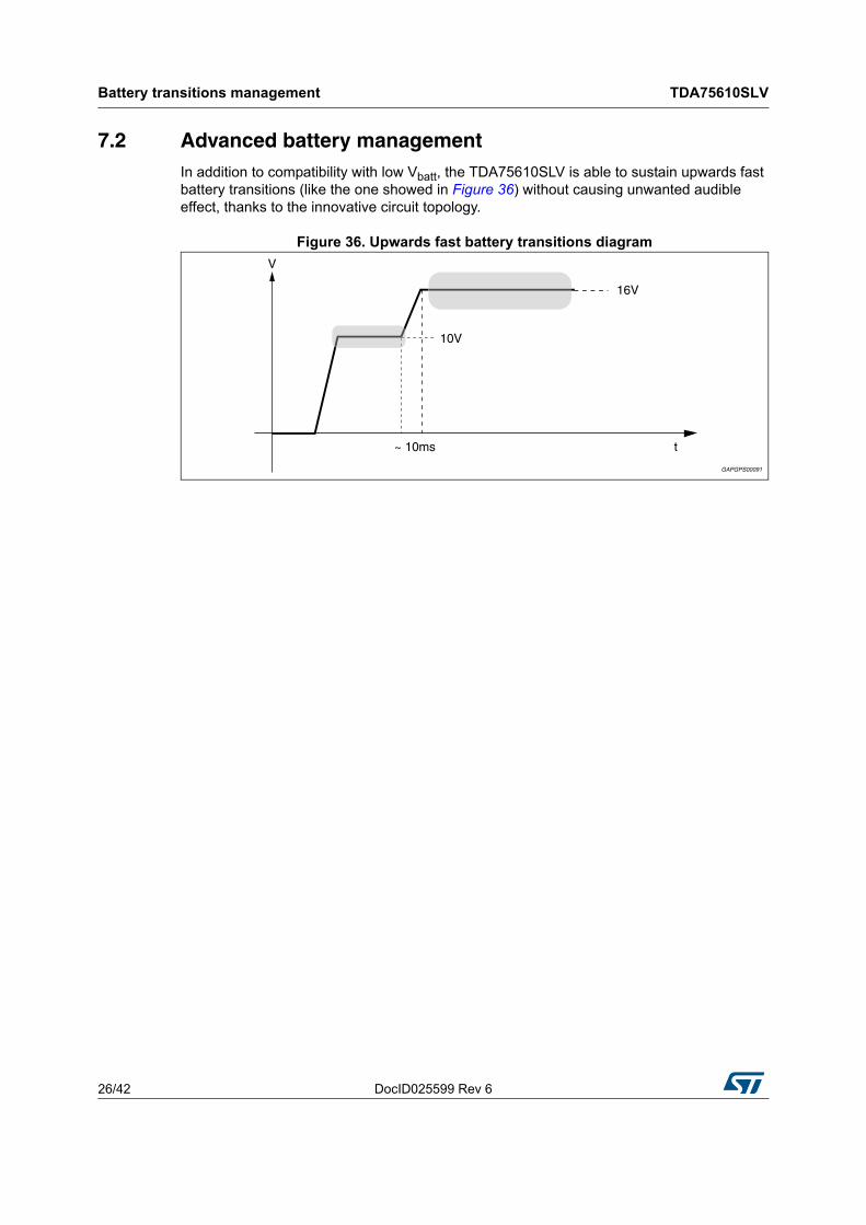
7.2 Advanced battery managementIn addition to compatibility with low Vbatt, the TDA75610SLV is able to sustain upwards fast battery transitions (like the one showed in Figure 36) without causing unwanted audible effect, thanks to the innovative circuit topology.
Figure 36. Upwards fast battery transitions diagram
DocID025599 Rev 6 27/42
TDA75610SLV Application suggestion
41
8 Application suggestion
8.1 Inputs impedance matching
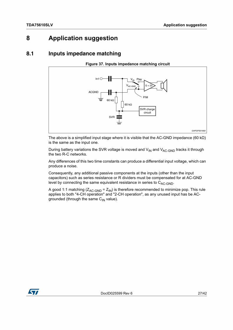
Figure 37. Inputs impedance matching circuit
The above is a simplified input stage where it is visible that the AC-GND impedance (60 kΩ) is the same as the input one.
During battery variations the SVR voltage is moved and VIN and VAC-GND tracks it through the two R-C networks.
Any differences of this two time constants can produce a differential input voltage, which can produce a noise.
Consequently, any additional passive components at the inputs (other than the input capacitors) such as series resistance or R dividers must be compensated for at AC-GND level by connecting the same equivalent resistance in series to CAC-GND.
A good 1:1 matching (ZAC-GND = ZIN) is therefore recommended to minimize pop. This rule applies to both "4-CH operation" and "2-CH operation", as any unused input has be AC-grounded (through the same CIN value).
Application suggestion TDA75610SLV
28/42 DocID025599 Rev 6
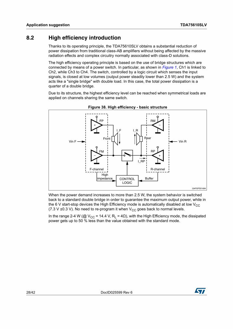
8.2 High efficiency introductionThanks to its operating principle, the TDA75610SLV obtains a substantial reduction of power dissipation from traditional class-AB amplifiers without being affected by the massive radiation effects and complex circuitry normally associated with class-D solutions.
The high efficiency operating principle is based on the use of bridge structures which are connected by means of a power switch. In particular, as shown in Figure 1, Ch1 is linked to Ch2, while Ch3 to Ch4. The switch, controlled by a logic circuit which senses the input signals, is closed at low volumes (output power steadily lower than 2.5 W) and the system acts like a "single bridge" with double load. In this case, the total power dissipation is a quarter of a double bridge.
Due to its structure, the highest efficiency level can be reached when symmetrical loads are applied on channels sharing the same switch.
Figure 38. High efficiency - basic structure
When the power demand increases to more than 2.5 W, the system behavior is switched back to a standard double bridge in order to guarantee the maximum output power, while in the 6 V start-stop devices the High Efficiency mode is automatically disabled at low VCC (7.3 V ±0.3 V). No need to re-program it when VCC goes back to normal levels.
In the range 2-4 W (@ VCC = 14.4 V, RL = 4Ω), with the High Efficiency mode, the dissipated power gets up to 50 % less than the value obtained with the standard mode.
DocID025599 Rev 6 29/42
TDA75610SLV I2C bus
41
9 I2C bus
9.1 I2C programming/reading sequences A correct turn on/off sequence with respect to the diagnostic timings and producing no
audible noises could be as follows (after battery connection):
TURN-ON: PIN2 > 4.5 V --- 10 ms --- (STAND-BY OUT + DIAG ENABLE) --- 1 s (min) --- MUTING OUT
TURN-OFF: MUTING IN - wait for 50 ms - HW ST-BY IN (ST-BY pin . 1.2 V)
Car Radio Installation: PIN2 > 4.5 V --- 10 ms DIAG ENABLE (write) --- 200 ms --- I2C read (repeat until All faults disappear).
OFFSET TEST: Device in Play (no signal) -- OFFSET ENABLE - 30 ms - I2C reading (repeat I2C reading until high-offset message disappears).
9.2 Address selection and I2C disableWhen the ADSEL/I2CDIS pin is left open the I2C bus is disabled and the device can be controlled by the STBY/MUTE pin.
In this status (no - I2C bus) the CK pin enables the HIGH-EFFICIENCY MODE (0 = STD MODE; 1 = HE MODE) and the DATA pin sets the gain (0 = 26 dB; 1 = 16 dB).
When the ADSEL/I2CDIS pin is connected to GND the I2C bus is active with address <1101100-x>.
To select the other I2C address a resistor must be connected to ADSEL/I2CDIS pin as following:
0 < R < 1 kΩ: I2C bus active with address <1101100x>
11 kΩ < R < 21 kΩ: I2C bus active with address <1101101x>
40 kΩ < R < 70 kΩ: I2C bus active with address <1101110x>
R > 120 kΩ: Legacy mode
(x: read/write bit sector)
9.3 I2C bus interfaceData transmission from microprocessor to the TDA75610SLV and viceversa takes place through the 2 wires I2C bus interface, consisting of the two lines SDA and SCL (pull-up resistors to positive supply voltage must be connected).
9.3.1 Data validity
As shown by Figure 39, the data on the SDA line must be stable during the high period of the clock. The HIGH and LOW state of the data line can only change when the clock signal on the SCL line is LOW.
I2C bus TDA75610SLV
30/42 DocID025599 Rev 6
9.3.2 Start and stop conditions
As shown by Figure 40 a start condition is a HIGH to LOW transition of the SDA line while SCL is HIGH. The stop condition is a LOW to HIGH transition of the SDA line while SCL is HIGH.
9.3.3 Byte format
Every byte transferred to the SDA line must contain 8 bits. Each byte must be followed by an acknowledge bit. The MSB is transferred first.
9.3.4 Acknowledge
The transmitter* puts a resistive HIGH level on the SDA line during the acknowledge clock pulse (see Figure 41). The receiver** has to pull-down (LOW) the SDA line during the acknowledge clock pulse, so that the SDA line is stable LOW during this clock pulse.
* Transmitter
– master µP) when it writes an address to the TDA75610SLV
– slave (TDA75610SLV) when the µP reads a data byte from TDA75610SLV
** Receiver
– slave (TDA75610SLV) when the µP writes an address to the TDA75610SLV
– master (µP) when it reads a data byte from TDA75610SLV
Figure 39. Data validity on the I2C bus
Figure 40. Timing diagram on the I2C bus
Figure 41. Acknowledge on the I2C bus
DocID025599 Rev 6 31/42
TDA75610SLV Software specifications
41
10 Software specifications
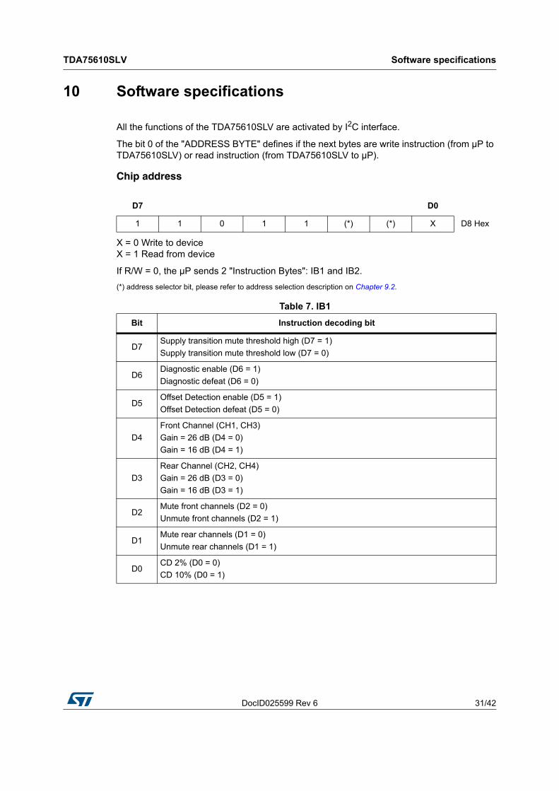
All the functions of the TDA75610SLV are activated by I2C interface.
The bit 0 of the "ADDRESS BYTE" defines if the next bytes are write instruction (from µP to TDA75610SLV) or read instruction (from TDA75610SLV to µP).
Chip address
X = 0 Write to deviceX = 1 Read from device
If R/W = 0, the µP sends 2 "Instruction Bytes": IB1 and IB2.
(*) address selector bit, please refer to address selection description on Chapter 9.2.
D7 D0
1 1 0 1 1 (*) (*) X D8 Hex
Table 7. IB1
Bit Instruction decoding bit
D7Supply transition mute threshold high (D7 = 1)
Supply transition mute threshold low (D7 = 0)
D6Diagnostic enable (D6 = 1)
Diagnostic defeat (D6 = 0)
D5Offset Detection enable (D5 = 1)
Offset Detection defeat (D5 = 0)
D4
Front Channel (CH1, CH3)
Gain = 26 dB (D4 = 0)
Gain = 16 dB (D4 = 1)
D3
Rear Channel (CH2, CH4)
Gain = 26 dB (D3 = 0)
Gain = 16 dB (D3 = 1)
D2Mute front channels (D2 = 0)
Unmute front channels (D2 = 1)
D1Mute rear channels (D1 = 0)
Unmute rear channels (D1 = 1)
D0CD 2% (D0 = 0)
CD 10% (D0 = 1)
Software specifications TDA75610SLV
32/42 DocID025599 Rev 6
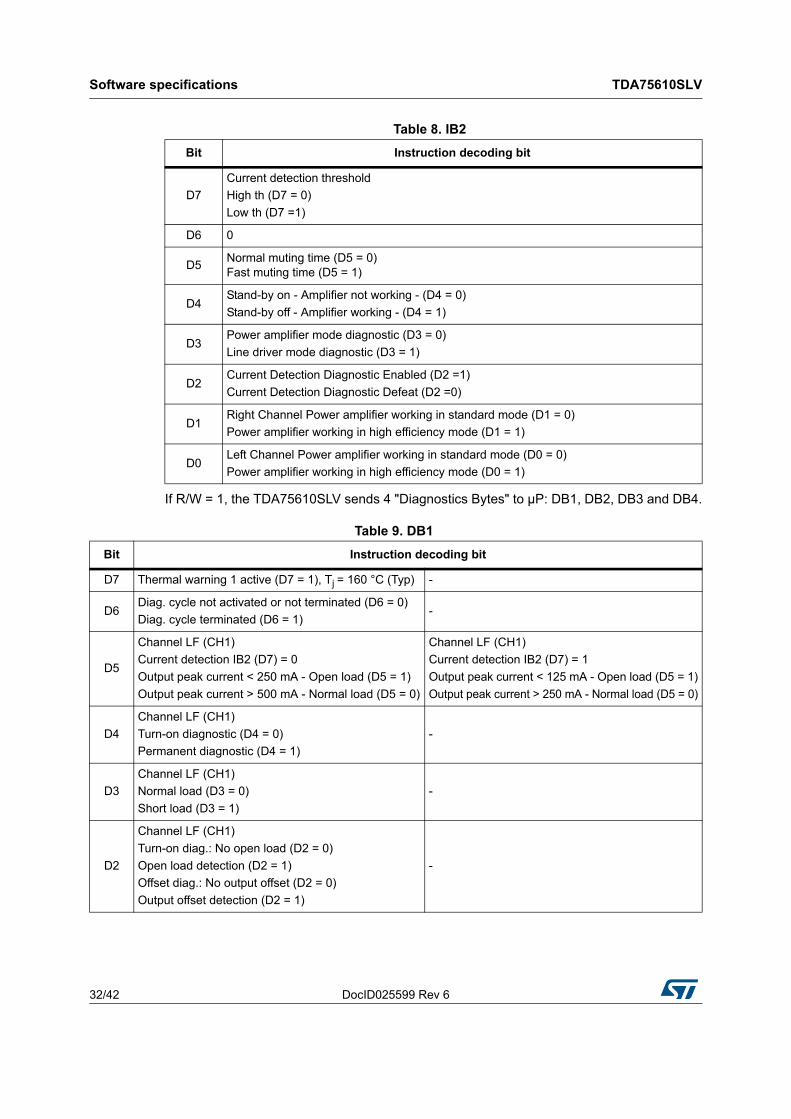
If R/W = 1, the TDA75610SLV sends 4 "Diagnostics Bytes" to µP: DB1, DB2, DB3 and DB4.
Table 8. IB2
Bit Instruction decoding bit
D7
Current detection threshold
High th (D7 = 0)
Low th (D7 =1)
D6 0
D5Normal muting time (D5 = 0)Fast muting time (D5 = 1)
D4Stand-by on - Amplifier not working - (D4 = 0)
Stand-by off - Amplifier working - (D4 = 1)
D3Power amplifier mode diagnostic (D3 = 0)
Line driver mode diagnostic (D3 = 1)
D2Current Detection Diagnostic Enabled (D2 =1)
Current Detection Diagnostic Defeat (D2 =0)
D1Right Channel Power amplifier working in standard mode (D1 = 0)
Power amplifier working in high efficiency mode (D1 = 1)
D0Left Channel Power amplifier working in standard mode (D0 = 0)
Power amplifier working in high efficiency mode (D0 = 1)
Table 9. DB1
Bit Instruction decoding bit
D7 Thermal warning 1 active (D7 = 1), Tj = 160 °C (Typ) -
D6Diag. cycle not activated or not terminated (D6 = 0)
Diag. cycle terminated (D6 = 1)-
D5
Channel LF (CH1)
Current detection IB2 (D7) = 0
Output peak current < 250 mA - Open load (D5 = 1)
Output peak current > 500 mA - Normal load (D5 = 0)
Channel LF (CH1)
Current detection IB2 (D7) = 1
Output peak current < 125 mA - Open load (D5 = 1)
Output peak current > 250 mA - Normal load (D5 = 0)
D4
Channel LF (CH1)
Turn-on diagnostic (D4 = 0)
Permanent diagnostic (D4 = 1)
-
D3
Channel LF (CH1)
Normal load (D3 = 0)
Short load (D3 = 1)
-
D2
Channel LF (CH1)
Turn-on diag.: No open load (D2 = 0)
Open load detection (D2 = 1)
Offset diag.: No output offset (D2 = 0)
Output offset detection (D2 = 1)
-
DocID025599 Rev 6 33/42
TDA75610SLV Software specifications
41
D1
Channel LF (CH1)
No short to Vcc (D1 = 0)
Short to Vcc (D1 = 1)
-
D0
Channel LF (CH1)
No short to GND (D1 = 0)
Short to GND (D1 = 1)
-
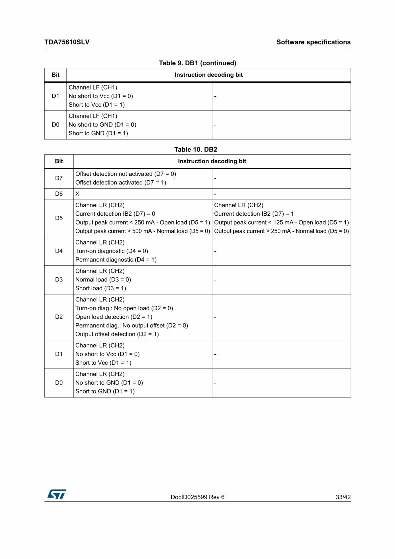
Table 9. DB1 (continued)
Bit Instruction decoding bit
Table 10. DB2
Bit Instruction decoding bit
D7Offset detection not activated (D7 = 0)
Offset detection activated (D7 = 1)-
D6 X -
D5
Channel LR (CH2)
Current detection IB2 (D7) = 0
Output peak current < 250 mA - Open load (D5 = 1)
Output peak current > 500 mA - Normal load (D5 = 0)
Channel LR (CH2)
Current detection IB2 (D7) = 1
Output peak current < 125 mA - Open load (D5 = 1)
Output peak current > 250 mA - Normal load (D5 = 0)
D4
Channel LR (CH2)
Turn-on diagnostic (D4 = 0)
Permanent diagnostic (D4 = 1)
-
D3
Channel LR (CH2)
Normal load (D3 = 0)
Short load (D3 = 1)
-
D2
Channel LR (CH2)
Turn-on diag.: No open load (D2 = 0)
Open load detection (D2 = 1)
Permanent diag.: No output offset (D2 = 0)
Output offset detection (D2 = 1)
-
D1
Channel LR (CH2)
No short to Vcc (D1 = 0)
Short to Vcc (D1 = 1)
-
D0
Channel LR (CH2)
No short to GND (D1 = 0)
Short to GND (D1 = 1)
-
Software specifications TDA75610SLV
34/42 DocID025599 Rev 6
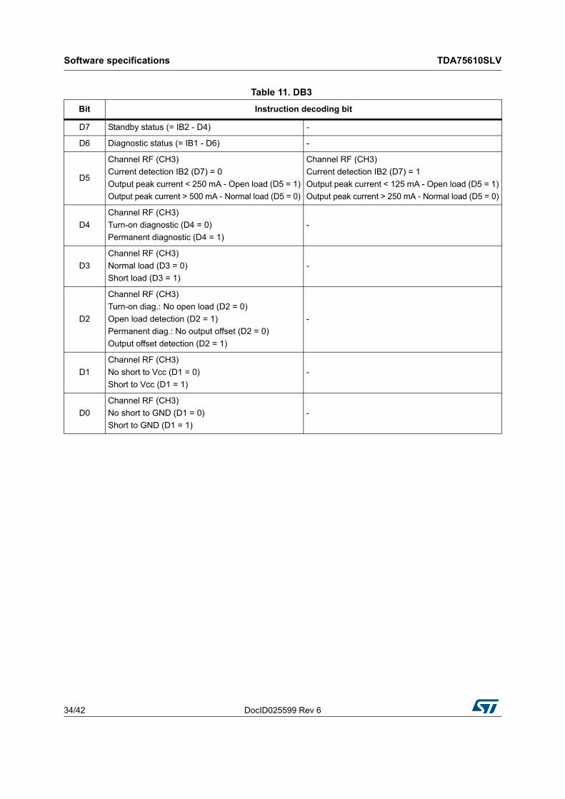
Table 11. DB3
Bit Instruction decoding bit
D7 Standby status (= IB2 - D4) -
D6 Diagnostic status (= IB1 - D6) -
D5
Channel RF (CH3)
Current detection IB2 (D7) = 0
Output peak current < 250 mA - Open load (D5 = 1)
Output peak current > 500 mA - Normal load (D5 = 0)
Channel RF (CH3)
Current detection IB2 (D7) = 1
Output peak current < 125 mA - Open load (D5 = 1)
Output peak current > 250 mA - Normal load (D5 = 0)
D4
Channel RF (CH3)
Turn-on diagnostic (D4 = 0)
Permanent diagnostic (D4 = 1)
-
D3
Channel RF (CH3)
Normal load (D3 = 0)
Short load (D3 = 1)
-
D2
Channel RF (CH3)
Turn-on diag.: No open load (D2 = 0)
Open load detection (D2 = 1)
Permanent diag.: No output offset (D2 = 0)
Output offset detection (D2 = 1)
-
D1
Channel RF (CH3)
No short to Vcc (D1 = 0)
Short to Vcc (D1 = 1)
-
D0
Channel RF (CH3)
No short to GND (D1 = 0)
Short to GND (D1 = 1)
-
DocID025599 Rev 6 35/42
TDA75610SLV Software specifications
41
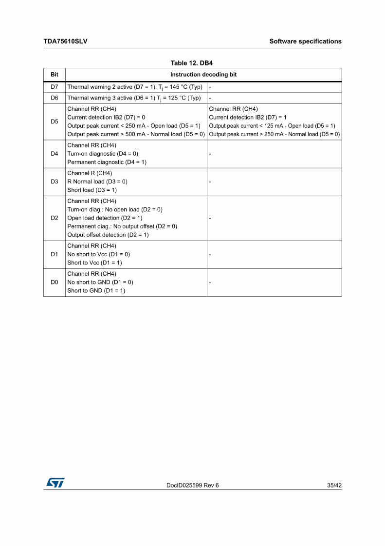
Table 12. DB4
Bit Instruction decoding bit
D7 Thermal warning 2 active (D7 = 1), Tj = 145 °C (Typ) -
D6 Thermal warning 3 active (D6 = 1) Tj = 125 °C (Typ) -
D5
Channel RR (CH4)
Current detection IB2 (D7) = 0
Output peak current < 250 mA - Open load (D5 = 1)
Output peak current > 500 mA - Normal load (D5 = 0)
Channel RR (CH4)
Current detection IB2 (D7) = 1
Output peak current < 125 mA - Open load (D5 = 1)
Output peak current > 250 mA - Normal load (D5 = 0)
D4
Channel RR (CH4)
Turn-on diagnostic (D4 = 0)
Permanent diagnostic (D4 = 1)
-
D3
Channel R (CH4)
R Normal load (D3 = 0)
Short load (D3 = 1)
-
D2
Channel RR (CH4)
Turn-on diag.: No open load (D2 = 0)
Open load detection (D2 = 1)
Permanent diag.: No output offset (D2 = 0)
Output offset detection (D2 = 1)
-
D1
Channel RR (CH4)
No short to Vcc (D1 = 0)
Short to Vcc (D1 = 1)
-
D0
Channel RR (CH4)
No short to GND (D1 = 0)
Short to GND (D1 = 1)
-
Examples of bytes sequence TDA75610SLV
36/42 DocID025599 Rev 6
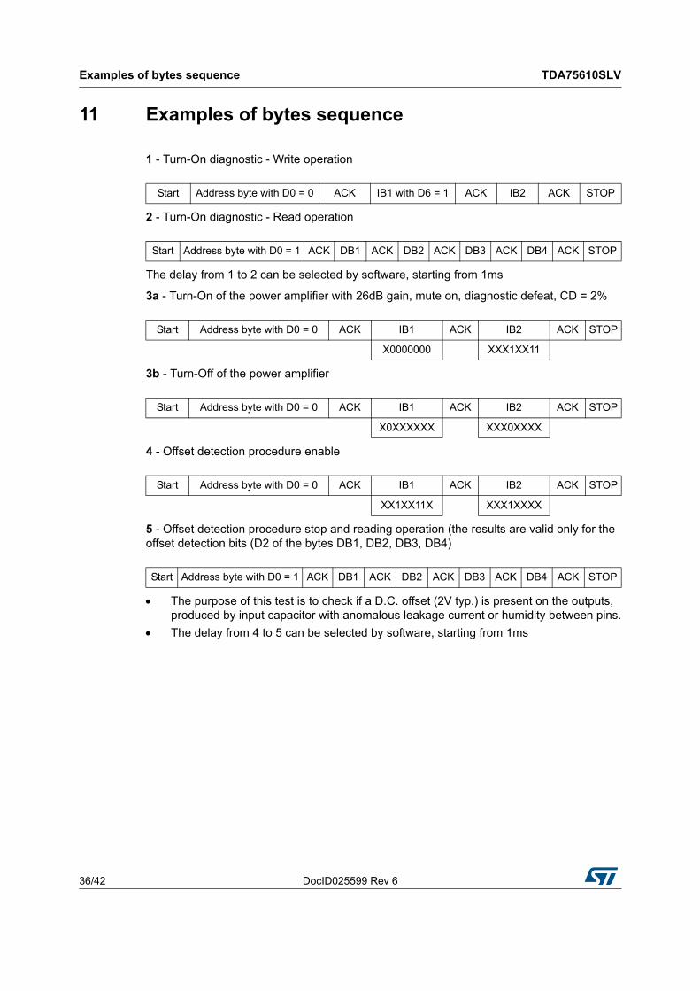
11 Examples of bytes sequence
1 - Turn-On diagnostic - Write operation
2 - Turn-On diagnostic - Read operation
The delay from 1 to 2 can be selected by software, starting from 1ms
3a - Turn-On of the power amplifier with 26dB gain, mute on, diagnostic defeat, CD = 2%
.
3b - Turn-Off of the power amplifier
4 - Offset detection procedure enable
5 - Offset detection procedure stop and reading operation (the results are valid only for the offset detection bits (D2 of the bytes DB1, DB2, DB3, DB4)
.
The purpose of this test is to check if a D.C. offset (2V typ.) is present on the outputs, produced by input capacitor with anomalous leakage current or humidity between pins.
The delay from 4 to 5 can be selected by software, starting from 1ms
Start Address byte with D0 = 0 ACK IB1 with D6 = 1 ACK IB2 ACK STOP
Start Address byte with D0 = 1 ACK DB1 ACK DB2 ACK DB3 ACK DB4 ACK STOP
Start Address byte with D0 = 0 ACK IB1 ACK IB2 ACK STOP
X0000000 XXX1XX11
Start Address byte with D0 = 0 ACK IB1 ACK IB2 ACK STOP
X0XXXXXX XXX0XXXX
Start Address byte with D0 = 0 ACK IB1 ACK IB2 ACK STOP
XX1XX11X XXX1XXXX
Start Address byte with D0 = 1 ACK DB1 ACK DB2 ACK DB3 ACK DB4 ACK STOP
DocID025599 Rev 6 37/42
TDA75610SLV Package information
41
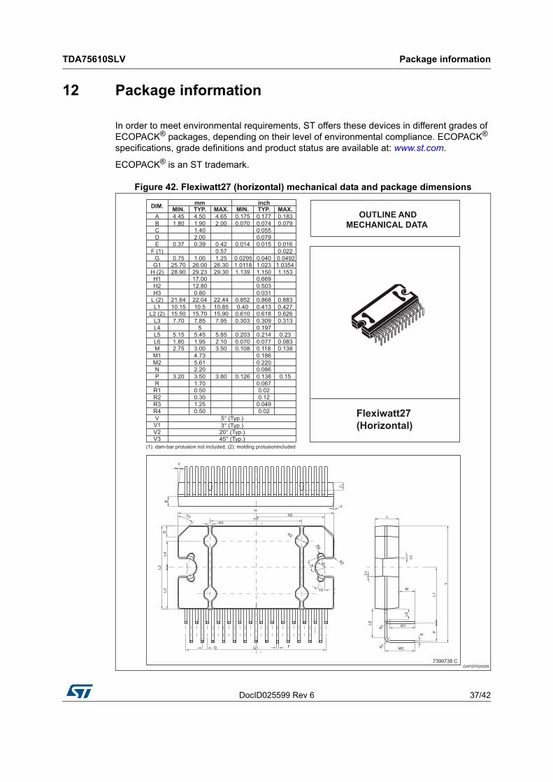
12 Package information
In order to meet environmental requirements, ST offers these devices in different grades of ECOPACK® packages, depending on their level of environmental compliance. ECOPACK® specifications, grade definitions and product status are available at: www.st.com.
ECOPACK® is an ST trademark.
Figure 42. Flexiwatt27 (horizontal) mechanical data and package dimensions
Package information TDA75610SLV
38/42 DocID025599 Rev 6
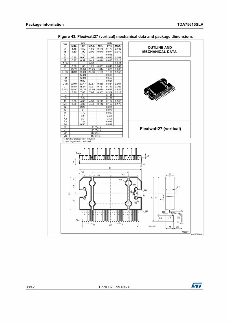
Figure 43. Flexiwatt27 (vertical) mechanical data and package dimensions
DocID025599 Rev 6 39/42
TDA75610SLV Package information
41
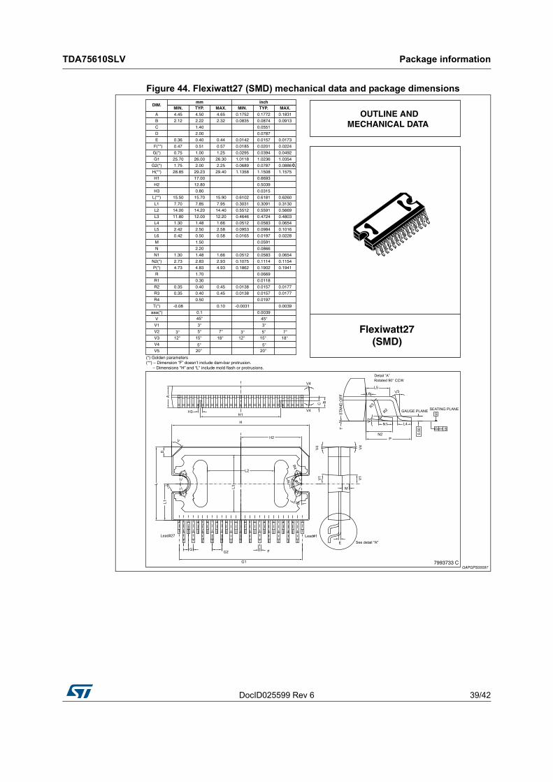
Figure 44. Flexiwatt27 (SMD) mechanical data and package dimensions
Package information TDA75610SLV
40/42 DocID025599 Rev 6
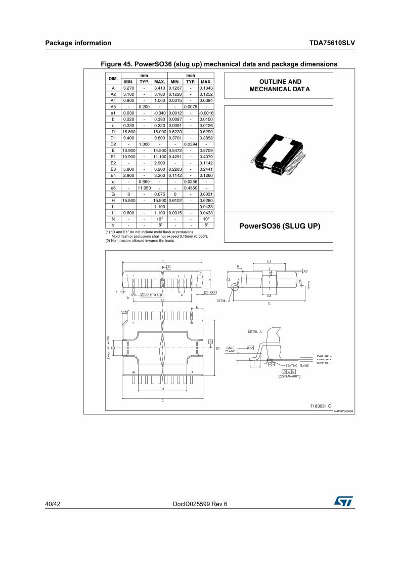
Figure 45. PowerSO36 (slug up) mechanical data and package dimensions
DocID025599 Rev 6 41/42
TDA75610SLV Revision history
41
13 Revision history
Table 13. Document revision history
Date Revision Changes
29-Nov-2013 1 Initial release.
10-Feb-2014 2Updated Section 9.1: I2C programming/reading sequences on page 29.
19-Mar-2014 3 Updated Figure 2 and Figure 3.
28-Apr-2014 4Updated Section 9.2: Address selection and I2C disable on page 29.
19-Sep-2014 5Updated Section 9.1: I2C programming/reading sequences on page 29.
15-Dec-2014 6 Corrected Figure 31 on page 22.

TDA75610SLV
42/42 DocID025599 Rev 6
IMPORTANT NOTICE – PLEASE READ CAREFULLY
STMicroelectronics NV and its subsidiaries (“ST”) reserve the right to make changes, corrections, enhancements, modifications, and improvements to ST products and/or to this document at any time without notice. Purchasers should obtain the latest relevant information on ST products before placing orders. ST products are sold pursuant to ST’s terms and conditions of sale in place at the time of order acknowledgement.
Purchasers are solely responsible for the choice, selection, and use of ST products and ST assumes no liability for application assistance or the design of Purchasers’ products.
No license, express or implied, to any intellectual property right is granted by ST herein.
Resale of ST products with provisions different from the information set forth herein shall void any warranty granted by ST for such product.
ST and the ST logo are trademarks of ST. All other product or service names are the property of their respective owners.
Information in this document supersedes and replaces information previously supplied in any prior versions of this document.
© 2014 STMicroelectronics – All rights reserved


![DATASHEET SEARCH SITE | ].pdf · 14 W × 4-Channel BTL Power IC ADE-207-116 1st. Edition Description The HA13151/HA13152 are high output and low distortion 4 ch BTL power IC designed](https://static.fdocument.org/doc/165x107/5fe49885db27a10ac0300364/datasheet-search-site-hitachipdf-14-w-4-channel-btl-power-ic-ade-207-116.jpg)