PLL and Frequency Synthesizer - GEOCITIES.ws
56
Fuding Ge: PLL and Frequency Synthesizer 2001 1 PLL and Frequency Synthesizer Fuding Ge, April 2001 • PLL fundamental • Self biased PLL • Fully differential PLL architecture • A3 rd order ∆Σ modulated fractional-N frequency synthesizer and its building blocks
Transcript of PLL and Frequency Synthesizer - GEOCITIES.ws
Fuding Ge: PLL and FrequencySynthesizer 2001
1
PLL and Frequency SynthesizerFuding Ge, April 2001
• PLL fundamental
• Self biased PLL
• Fully differential PLL architecture
• A 3rd order ∆Σ modulated fractional-N frequencysynthesizer and its building blocks
Fuding Ge: PLL and FrequencySynthesizer 2001
2
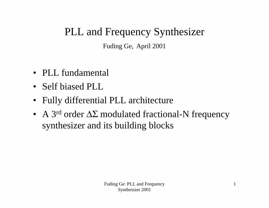
Fractional-N Frequency Synthesizer
PhaseDectector
Kpd
Low PasFilter
KlpHlp(s)
VCOKvco/s
FrequencyDivider
%N/N+1
Vref Ve Vc Vout
Vfb
Phase AccumulatorLacc
Overflow
divider ratio settingword Ldiv
Fuding Ge: PLL and FrequencySynthesizer 2001
3
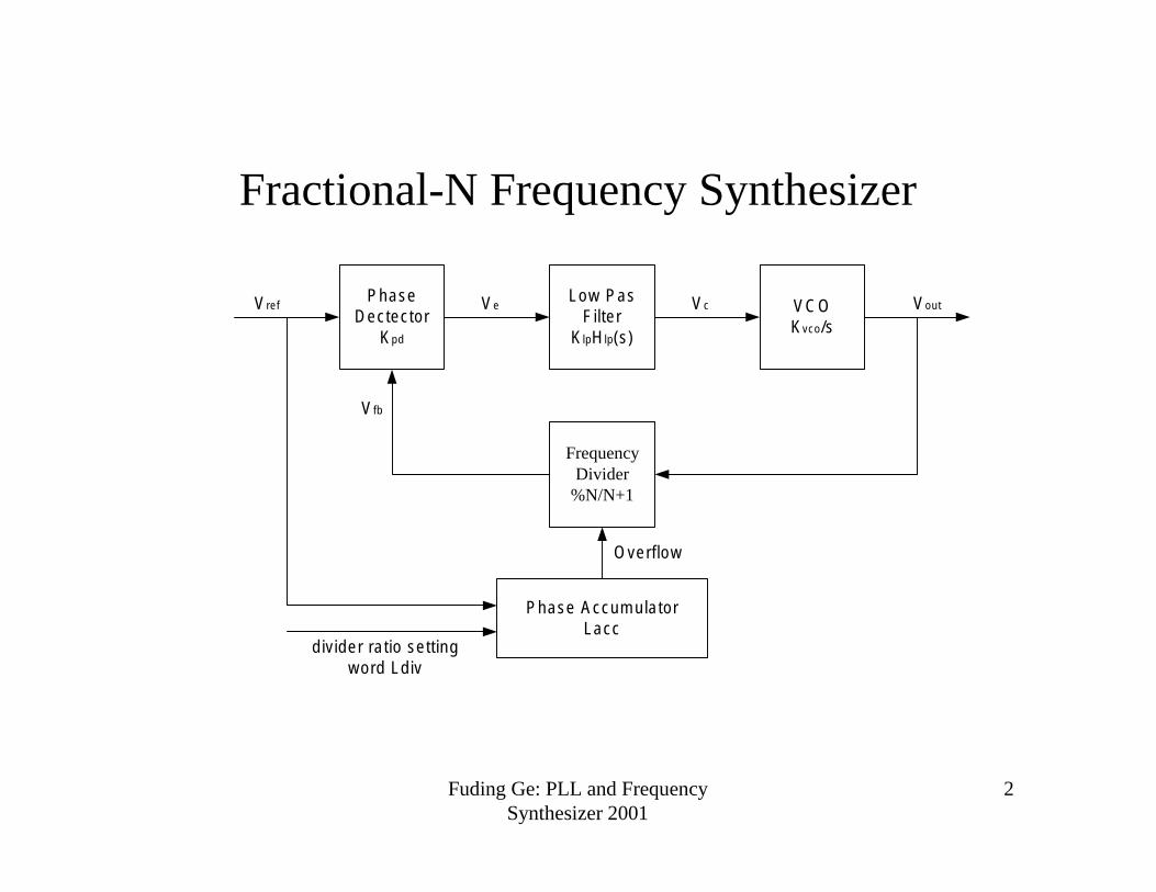
Spurious Tone
• V(t)=V0cos[ω0t+∆φsin(ωmt)]• If ∆φ<<π/2, then
V(t)=V0[cosω0t + ∆φcos(ω0+ωm)t/2− ∆φcos(ω0-ωm)t/2]
– The last two terms are spurious tone. One spur is ωm
above ω0 and one is ωm below ω0.
Fuding Ge: PLL and FrequencySynthesizer 2001
4
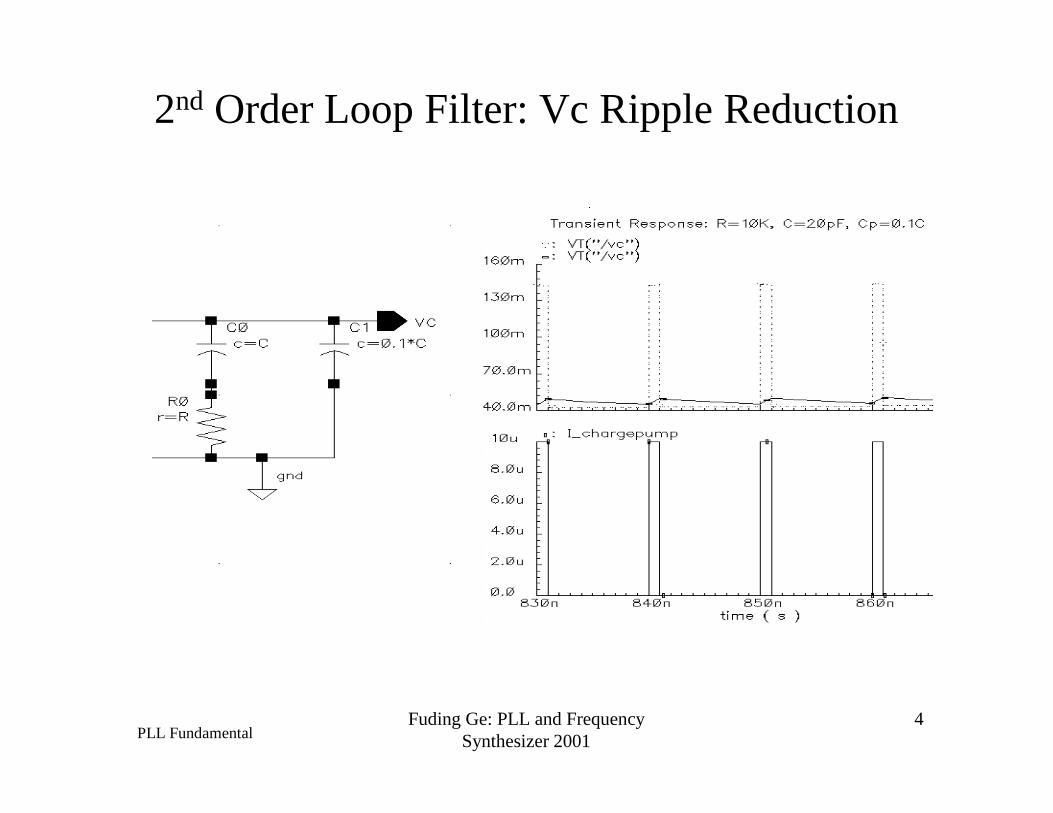
2nd Order Loop Filter: Vc Ripple Reduction
PLL Fundamental
Fuding Ge: PLL and FrequencySynthesizer 2001
5
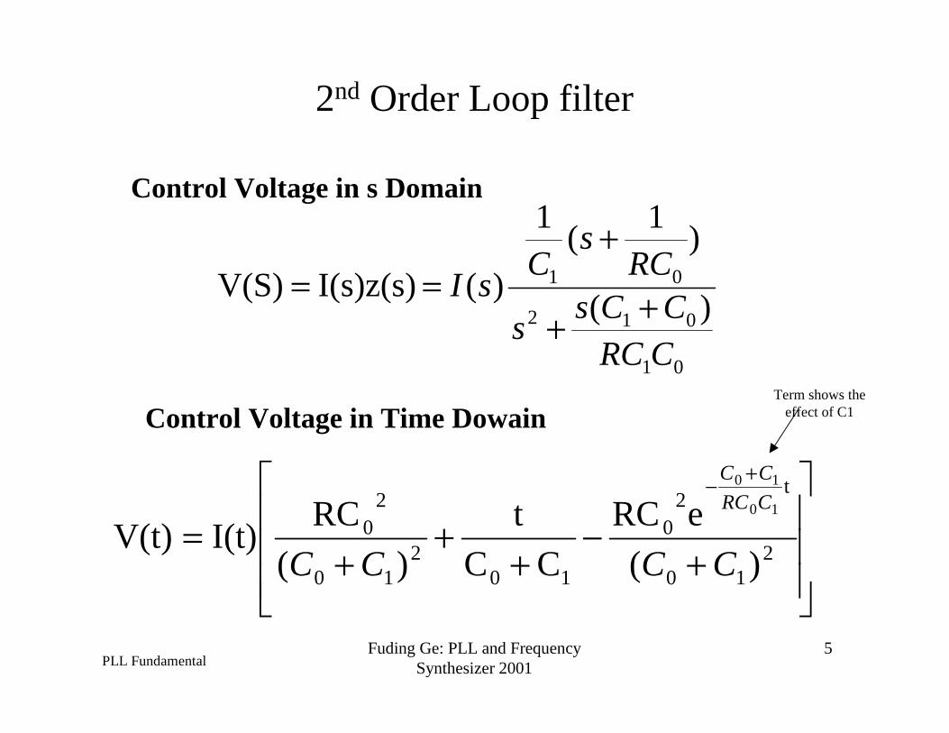
2nd Order Loop filter
01
012
01
)(
)1
(1
)(I(s)z(s)V(S)
CRC
CCss
RCs
CsI ++
+==
Control Voltage in s Domain
Control Voltage in Time Dowain
PLL Fundamental
+−
++
+=
+−
210
t2
0
102
10
20
)(
eRC
CC
t
)(
RCI(t)V(t)
10
10
CCCC
CRC
CC
Term shows theeffect of C1
Fuding Ge: PLL and FrequencySynthesizer 2001
6
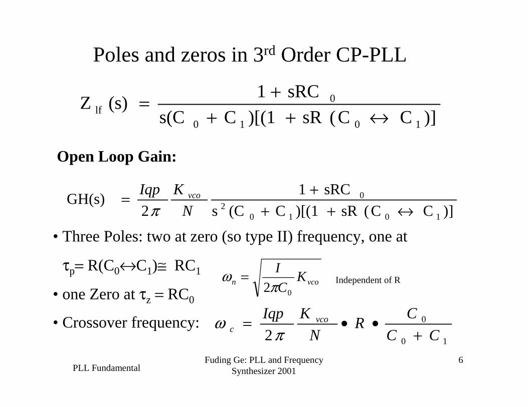
Poles and zeros in 3rd Order CP-PLL
)]CC(sR)[(1Cs(C
sRC1(s)Z
1010
0lf ↔++
+=
)]CC(sR)[(1C(Cs
sRC1
2GH(s)
10102
0
↔+++=
N
KIqp vco
π
Open Loop Gain:
• Three Poles: two at zero (so type II) frequency, one at
τp= R(C0↔C1)≅ RC1
• one Zero at τz = RC0
• Crossover frequency:10
0
2 CC
CR
N
KIqp vcoc +
••=π
ω
PLL Fundamental
vcon KC
I
02πω = Independent of R
Fuding Ge: PLL and FrequencySynthesizer 2001
7
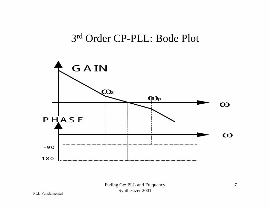
3rd Order CP-PLL: Bode Plot
ω
ω
ωz
ωp
GAIN
PHASE
-90
-180
PLL Fundamental
Fuding Ge: PLL and FrequencySynthesizer 2001
8
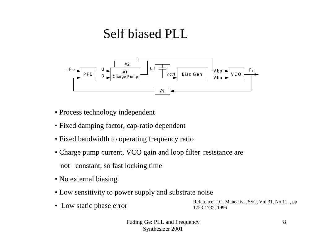
Self biased PLL
PFDU
D#1
Charge Pump
#2C1
Vctrl Bias GenVbp
VbnVCO
FoFref
/N
• Process technology independent
• Fixed damping factor, cap-ratio dependent
• Fixed bandwidth to operating frequency ratio
• Charge pump current, VCO gain and loop filter resistance are
not constant, so fast locking time
• No external biasing
• Low sensitivity to power supply and substrate noise
• Low static phase errorReference: J.G. Maneatis: JSSC, Vol 31, No.11, , pp1723-1732, 1996
Fuding Ge: PLL and FrequencySynthesizer 2001
9
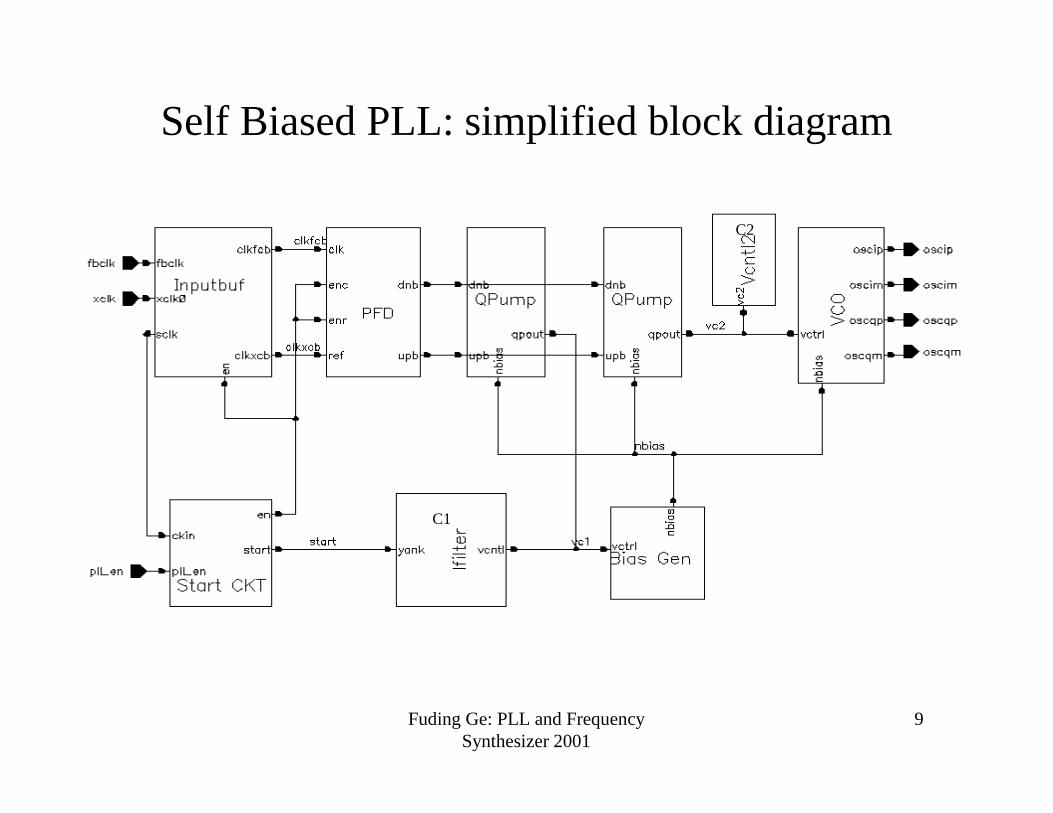
Self Biased PLL: simplified block diagram
C1
C2
Fuding Ge: PLL and FrequencySynthesizer 2001
10
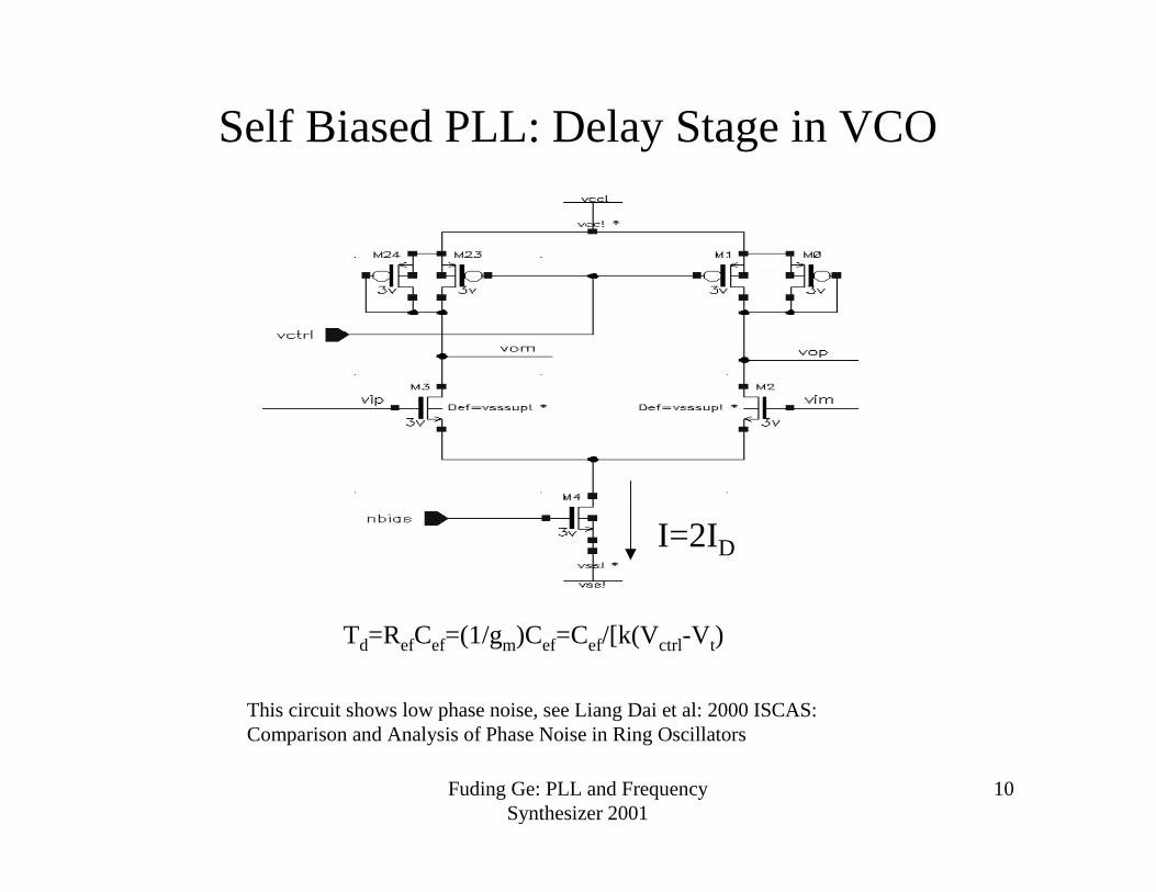
Self Biased PLL: Delay Stage in VCO
Td=RefCef=(1/gm)Cef=Cef/[k(Vctrl-Vt)
This circuit shows low phase noise, see Liang Dai et al: 2000 ISCAS:Comparison and Analysis of Phase Noise in Ring Oscillators
I=2ID
Fuding Ge: PLL and FrequencySynthesizer 2001
11
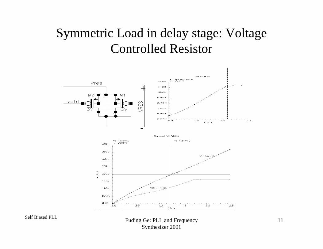
Symmetric Load in delay stage: VoltageControlled Resistor
Self Biased PLL
+
-
Fuding Ge: PLL and FrequencySynthesizer 2001
12
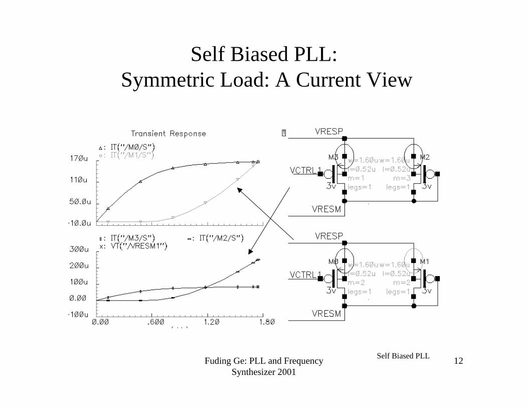
Self Biased PLL:Symmetric Load: A Current View
Self Biased PLL
Fuding Ge: PLL and FrequencySynthesizer 2001
13
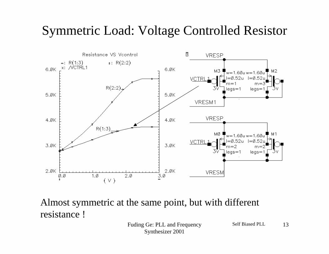
Symmetric Load: Voltage Controlled Resistor
Self Biased PLL
Almost symmetric at the same point, but with differentresistance !
Fuding Ge: PLL and FrequencySynthesizer 2001
14
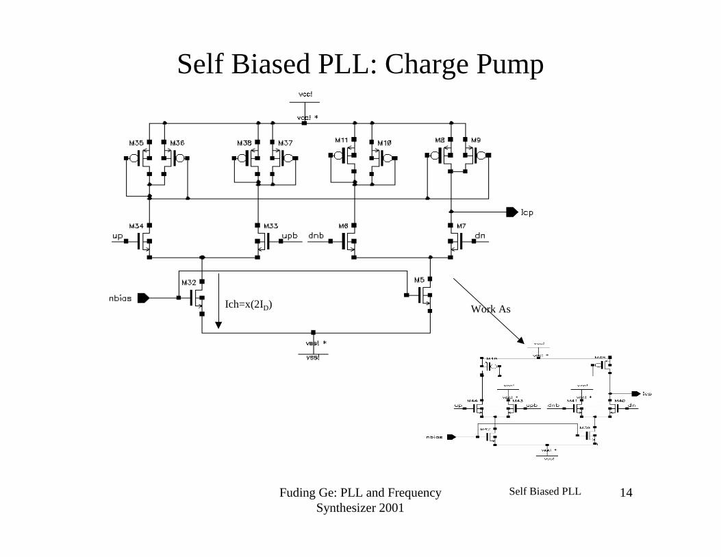
Self Biased PLL: Charge Pump
Work AsIch=x(2ID)
Self Biased PLL
Fuding Ge: PLL and FrequencySynthesizer 2001
15
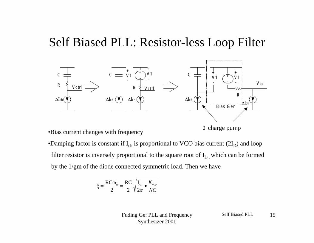
Self Biased PLL: Resistor-less Loop Filter
•Bias current changes with frequency
•Damping factor is constant if Ich is proportional to VCO bias current (2ID) and loop
filter resistor is inversely proportional to the square root of ID , which can be formed
by the 1/gm of the diode connected symmetric load. Then we have
NC
Kvco•==π2
I
2
RC
2
RCωξ chn
∆Ich
C
R Vctrl
∆Ich
C
Vctrl
V1+
-
+-
V1+
-
R
∆Ich ∆Ich
C V1+
-+-
V1+
-
R
∆Ich
Vbp
Bias Gen
2 charge pump
Self Biased PLL
Fuding Ge: PLL and FrequencySynthesizer 2001
16
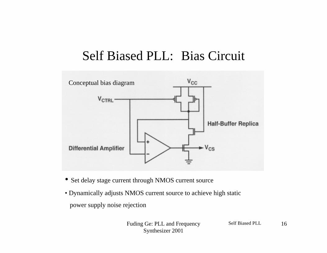
Self Biased PLL: Bias Circuit
Self Biased PLL
Conceptual bias diagram
• Set delay stage current through NMOS current source
• Dynamically adjusts NMOS current source to achieve high static
power supply noise rejection
Fuding Ge: PLL and FrequencySynthesizer 2001
17
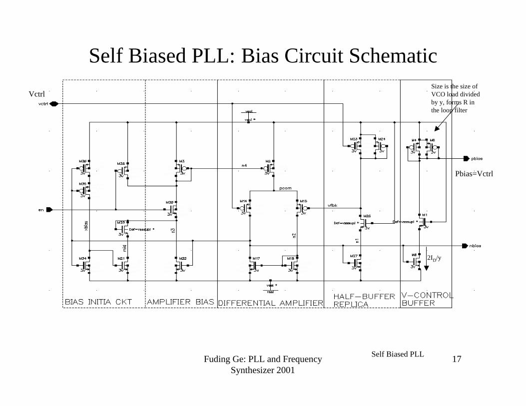
Self Biased PLL: Bias Circuit Schematic
Self Biased PLL
Vctrl
Pbias=Vctrl
Size is the size ofVCO load dividedby y, forms R inthe loop filter
2ID/y
Fuding Ge: PLL and FrequencySynthesizer 2001
18
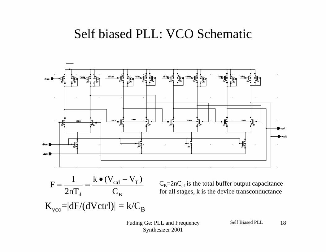
Self biased PLL: VCO Schematic
2ID
B
Tctrl
d C
)V(Vk
2nT
1F
−•== CB=2nCef is the total buffer output capacitancefor all stages, k is the device transconductance
Kvco=|dF/(dVctrl)| = k/CB
Self Biased PLL
Fuding Ge: PLL and FrequencySynthesizer 2001
19
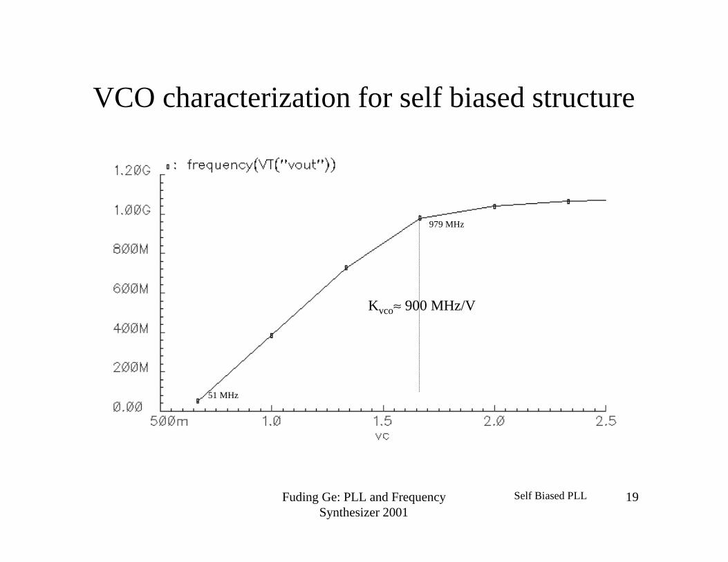
VCO characterization for self biased structure
51 MHz
979 MHz
Kvco≈ 900 MHz/V
Self Biased PLL
Fuding Ge: PLL and FrequencySynthesizer 2001
20
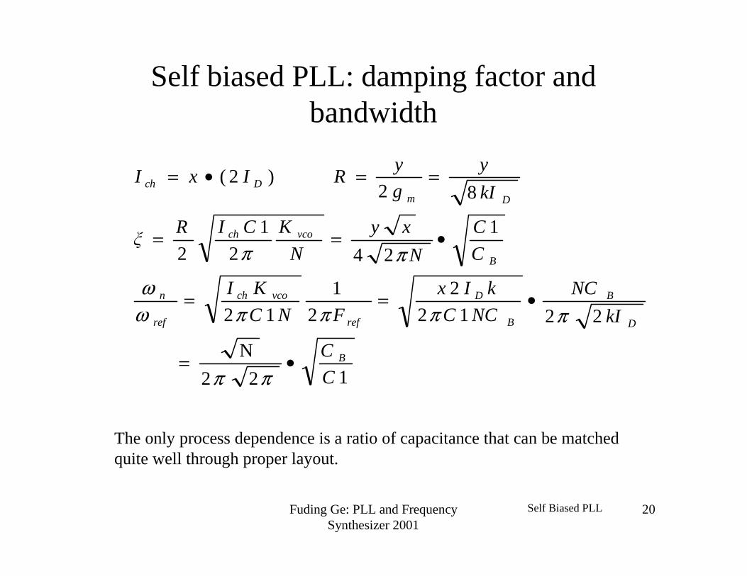
Self biased PLL: damping factor andbandwidth
122
N
2212
2
2
1
12
1
242
1
2
82)2(
C
C
kI
NC
NCC
kIx
FNC
KI
C
C
N
xy
N
KCIRξ
kI
y
g
yRIxI
B
D
B
B
D
ref
vcoch
ref
n
B
vcoch
DmDch
•=
•==
•==
==•=
ππ
ππππωω
ππ
The only process dependence is a ratio of capacitance that can be matchedquite well through proper layout.
Self Biased PLL
Fuding Ge: PLL and FrequencySynthesizer 2001
21
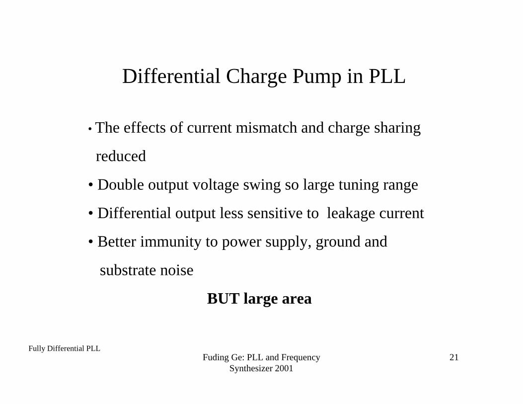
Differential Charge Pump in PLL
• The effects of current mismatch and charge sharing
reduced
• Double output voltage swing so large tuning range
• Differential output less sensitive to leakage current
• Better immunity to power supply, ground and
substrate noise
BUT large area
Fully Differential PLL
Fuding Ge: PLL and FrequencySynthesizer 2001
22
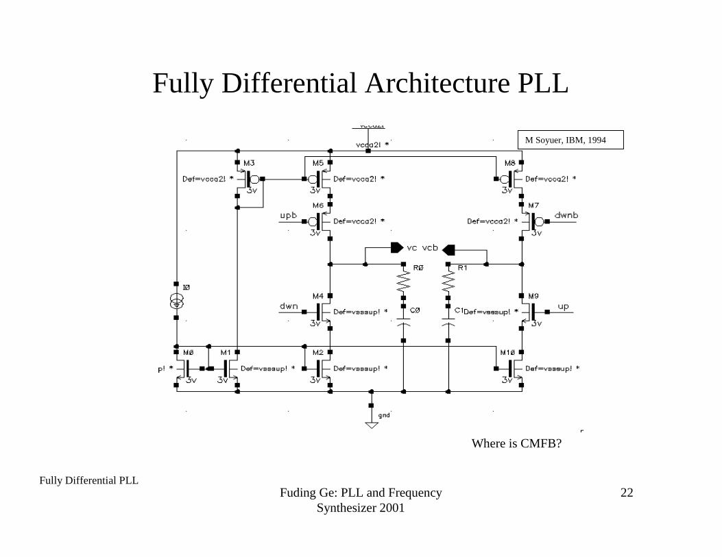
Fully Differential Architecture PLL
Fully Differential PLL
M Soyuer, IBM, 1994
Where is CMFB?
Fuding Ge: PLL and FrequencySynthesizer 2001
23
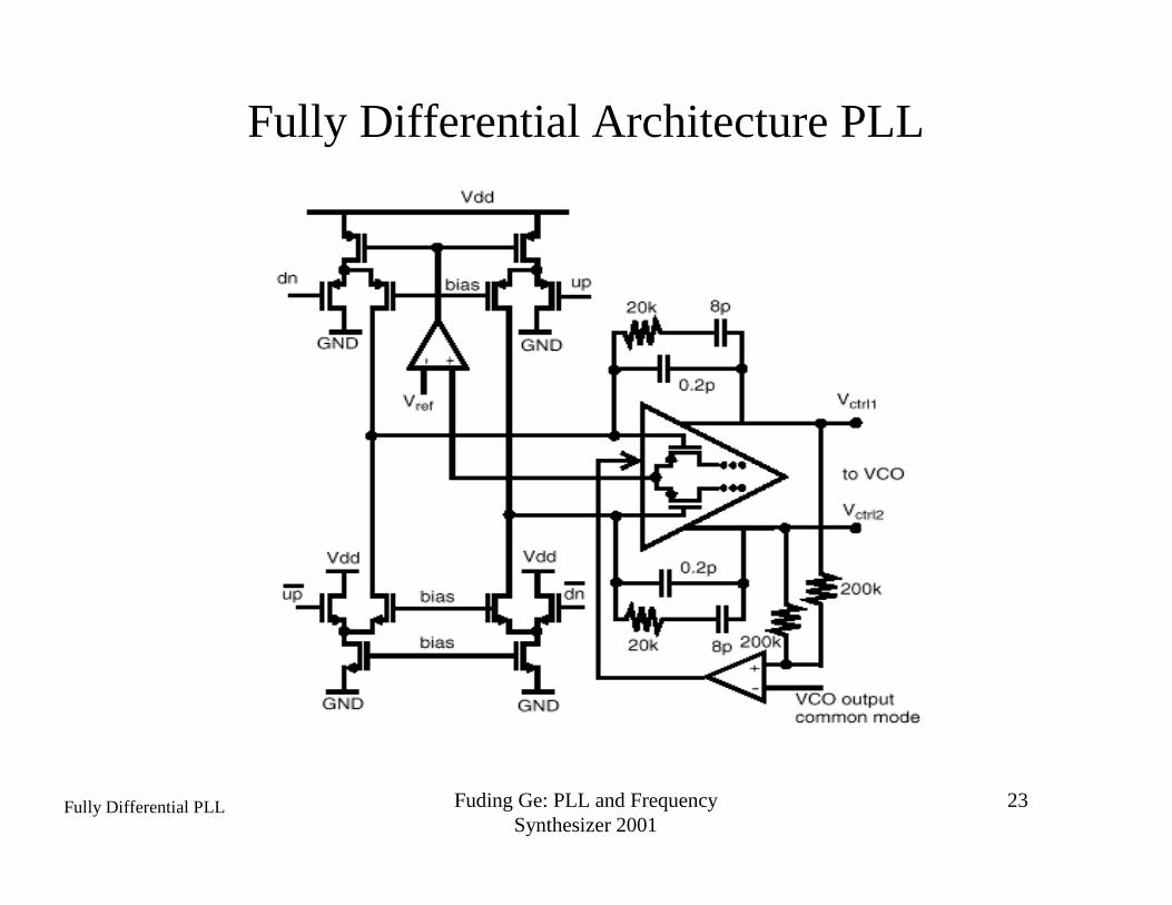
Fully Differential Architecture PLL
Fully Differential PLL
Fuding Ge: PLL and FrequencySynthesizer 2001
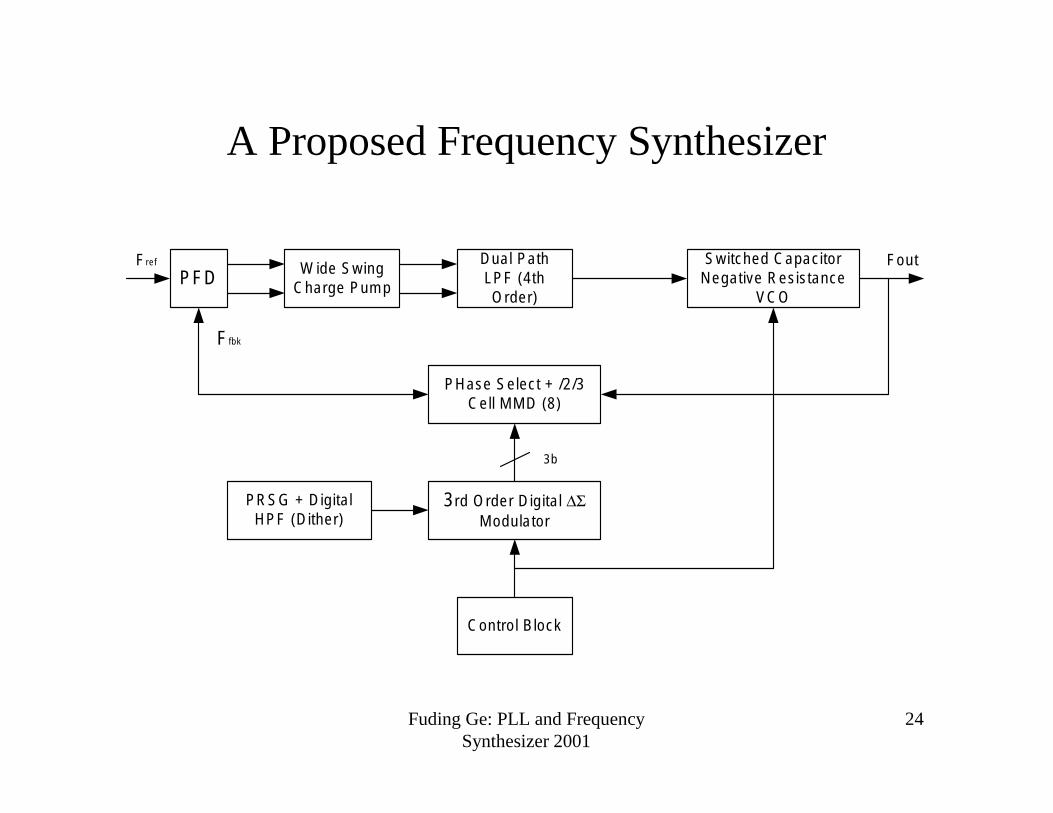
24
A Proposed Frequency Synthesizer
PFD Wide SwingCharge Pump
Switched CapacitorNegative Resistance
VCO
Dual PathLPF (4thOrder)
PHase Select + /2/3Cell MMD (8)
3rd Order Digital ∆ΣModulator
PRSG + DigitalHPF (Dither)
Control Block
Fref
3b
Fout
Ffbk
Fuding Ge: PLL and FrequencySynthesizer 2001
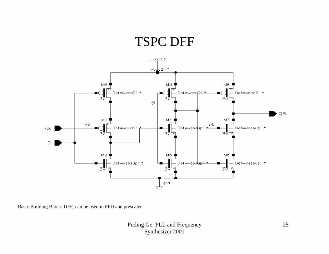
25
TSPC DFF
Basic Building Block: DFF, can be used in PFD and prescaler
Fuding Ge: PLL and FrequencySynthesizer 2001
26
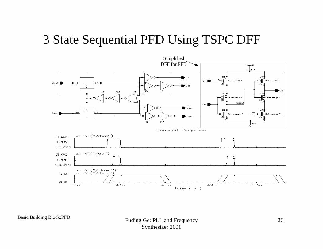
3 State Sequential PFD Using TSPC DFF
Basic Building Block:PFD
SimplifiedDFF for PFD

Fuding Ge: PLL and FrequencySynthesizer 2001
27
Charge Pump: Non-ideality
•Leakage Current: Phase error φε= 2πIleak/Icp
Reference spur:
fref=200Khz, fBW=20KHz, fout=2GHz, fpl=80KHz, Icp=1mA, Ileak=1nA, Pr=-55 dBc
Solution: Narrow bandwidth, Increase current (?)
•Mismatches in Charge Pump:
Phase error φε= 2π (∆I/Icp)(ton/Tref)Mismatch=10%, Pr=-47dBc
•Solution: Careful Circuit Design
•Timing Mismatch PFD
φ
= 2r2
22
log20Pref
plvcoecp
f
fKRI
π
Basic Building Block:Charge Pump
Fuding Ge: PLL and FrequencySynthesizer 2001
28
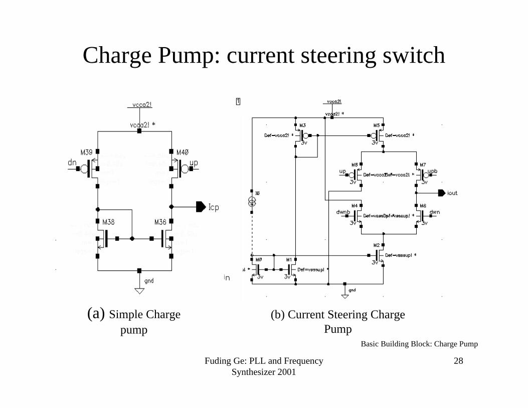
Charge Pump: current steering switch
Basic Building Block: Charge Pump
(a) Simple Chargepump
(b) Current Steering ChargePump
Fuding Ge: PLL and FrequencySynthesizer 2001
29
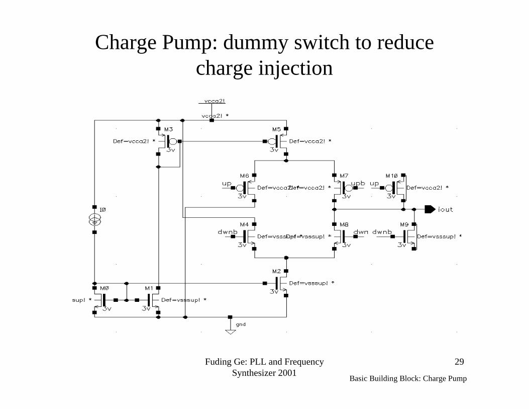
Charge Pump: dummy switch to reducecharge injection
Basic Building Block: Charge Pump
Fuding Ge: PLL and FrequencySynthesizer 2001
30
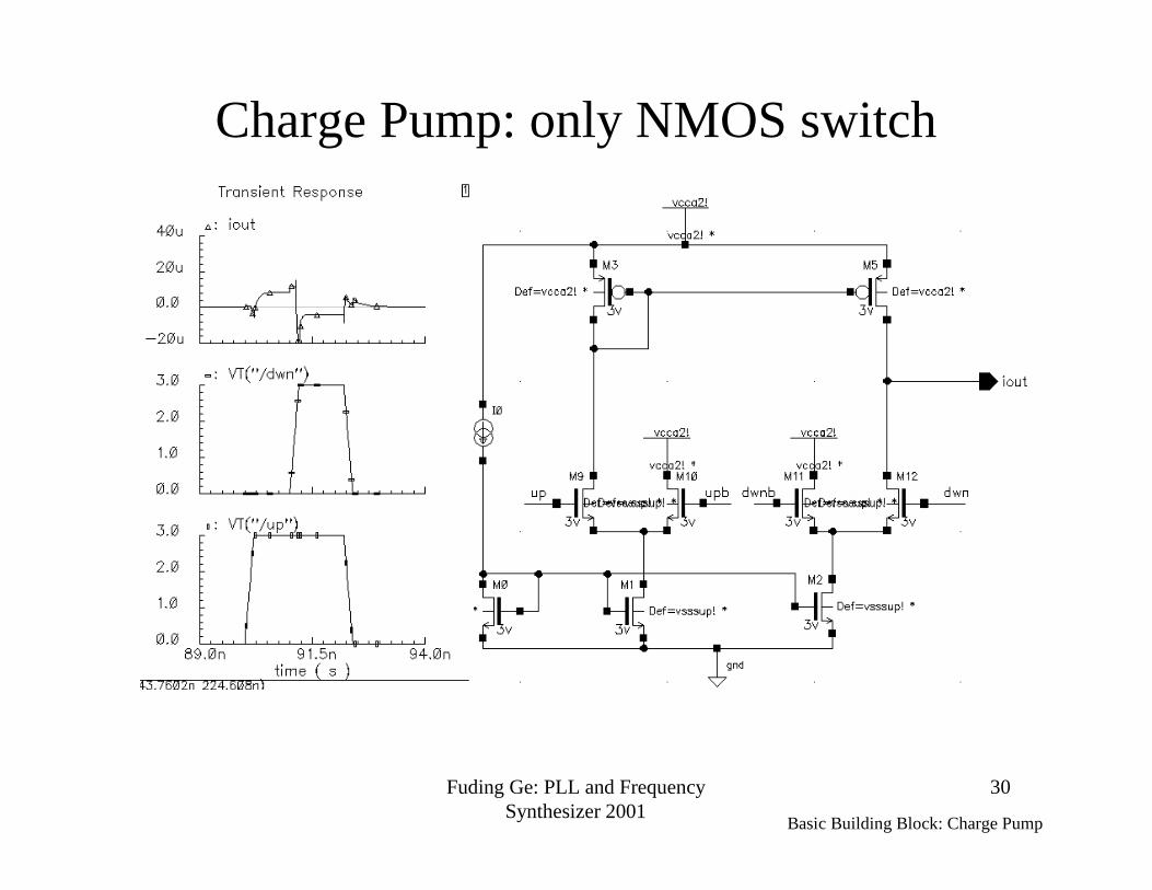
Charge Pump: only NMOS switch
Basic Building Block: Charge Pump
Fuding Ge: PLL and FrequencySynthesizer 2001
31
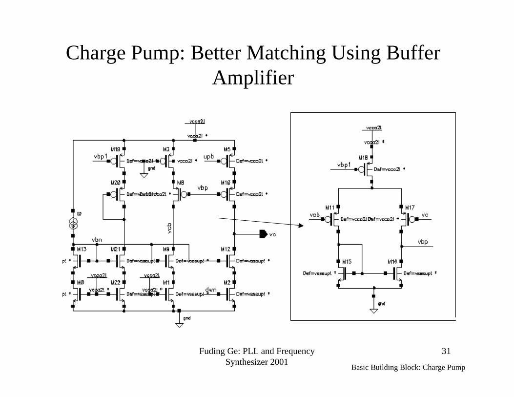
Charge Pump: Better Matching Using BufferAmplifier
Basic Building Block: Charge Pump
Fuding Ge: PLL and FrequencySynthesizer 2001
32
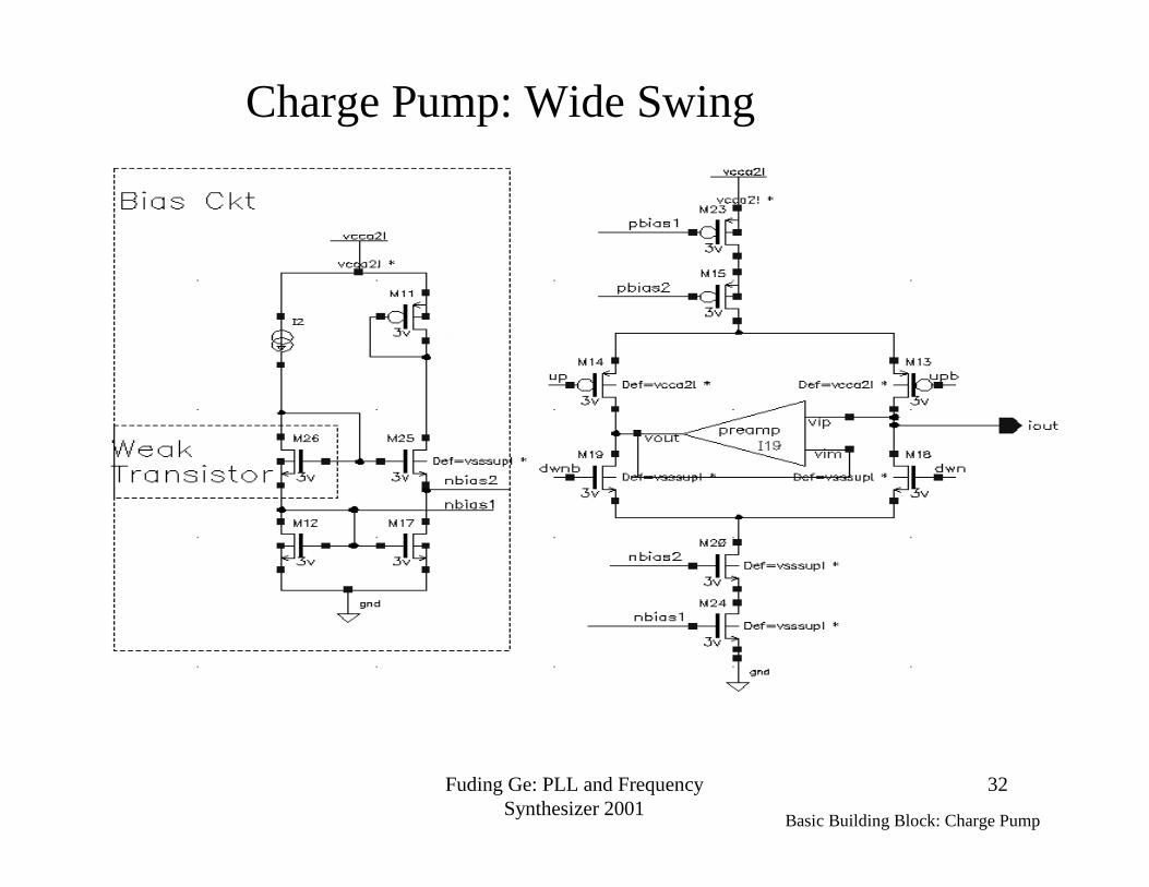
Charge Pump: Wide Swing
Basic Building Block: Charge Pump
Fuding Ge: PLL and FrequencySynthesizer 2001
33
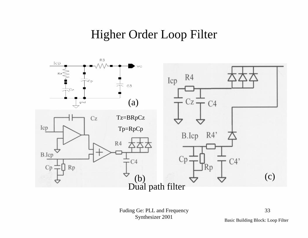
Higher Order Loop Filter
Basic Building Block: Loop Filter
Lo Chi Wa, HKUST, 2000
(b) (c)Dual path filter
(a)
Tz=BRpCz
Tp=RpCp
Fuding Ge: PLL and FrequencySynthesizer 2001
34
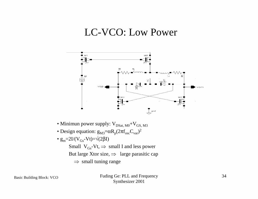
LC-VCO: Low Power
Basic Building Block: VCO
• Minimun power supply: VDSat, M0+VGS, M3
• Design equation: gM3=αRp(2πfoscCvar)2
• gm=2I/(VGs-Vt)=√(2βI)
Small VGs-Vt, ⇒ small I and less power
But large Xtor size, ⇒ large parasitic cap
⇒ small tuning range
Fuding Ge: PLL and FrequencySynthesizer 2001
35
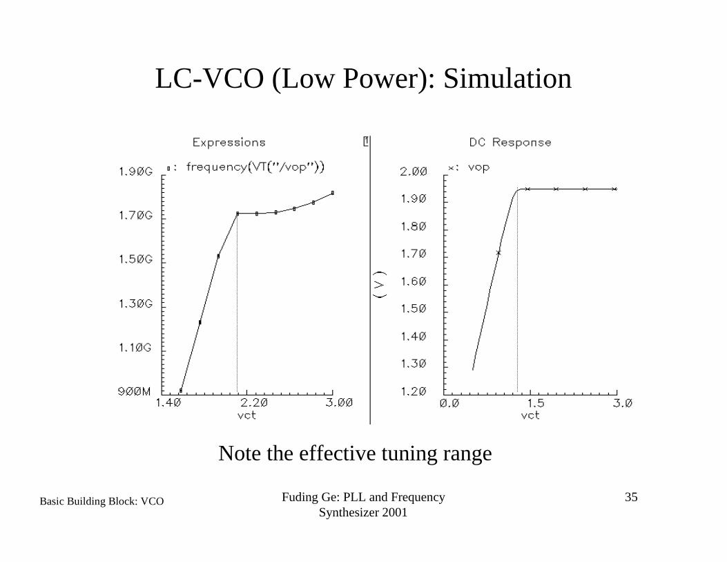
LC-VCO (Low Power): Simulation
Basic Building Block: VCO
Note the effective tuning range
Fuding Ge: PLL and FrequencySynthesizer 2001
36
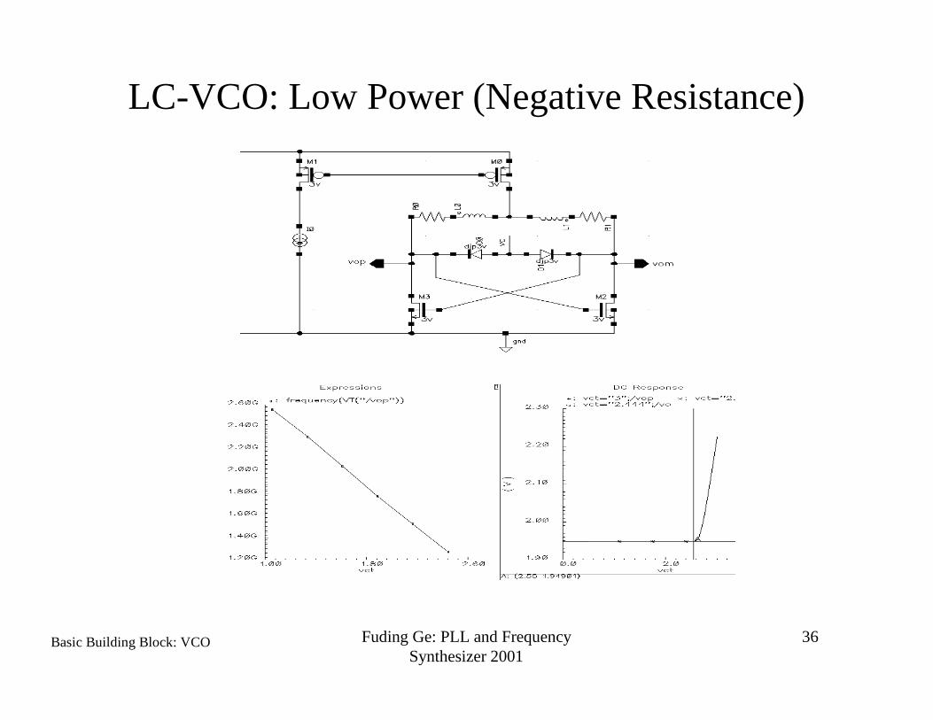
LC-VCO: Low Power (Negative Resistance)
Basic Building Block: VCO

Fuding Ge: PLL and FrequencySynthesizer 2001
37
LC-VCO: Tail Current Reuse
Basic Building Block: VCO
Fuding Ge: PLL and FrequencySynthesizer 2001
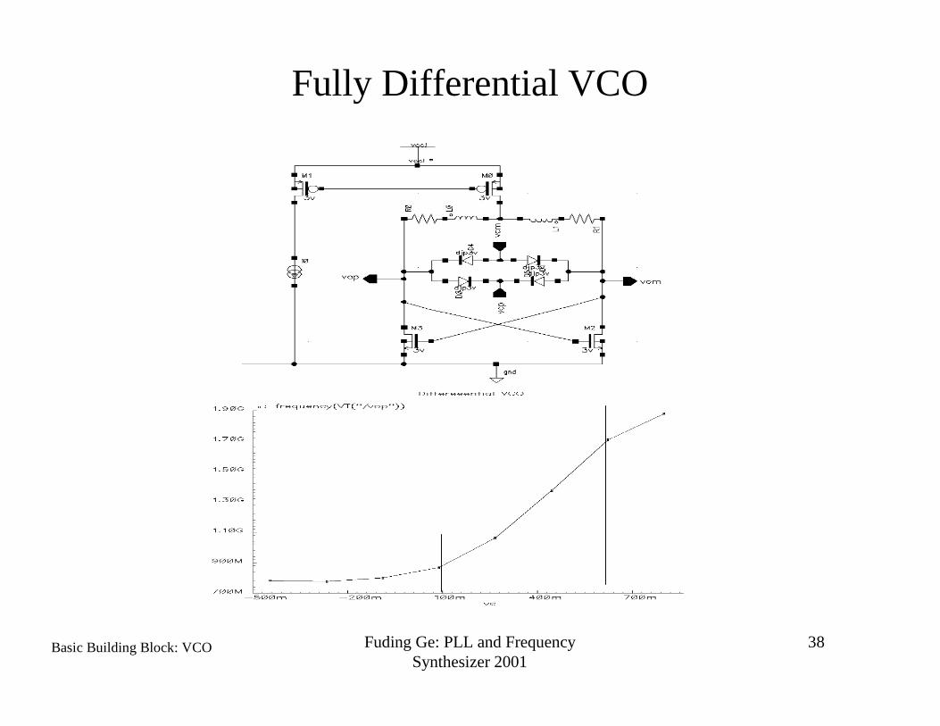
38
Fully Differential VCO
Basic Building Block: VCO
Fuding Ge: PLL and FrequencySynthesizer 2001
39
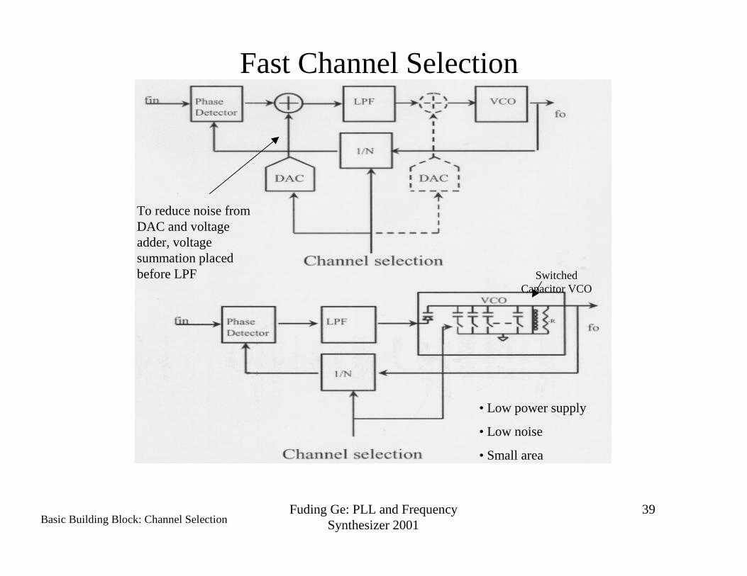
Fast Channel SelectionLo Chi Wa, HKUST, 2000
SwitchedCapacitor VCO
To reduce noise fromDAC and voltageadder, voltagesummation placedbefore LPF
• Low power supply
• Low noise
• Small area
Basic Building Block: Channel Selection
Fuding Ge: PLL and FrequencySynthesizer 2001
40
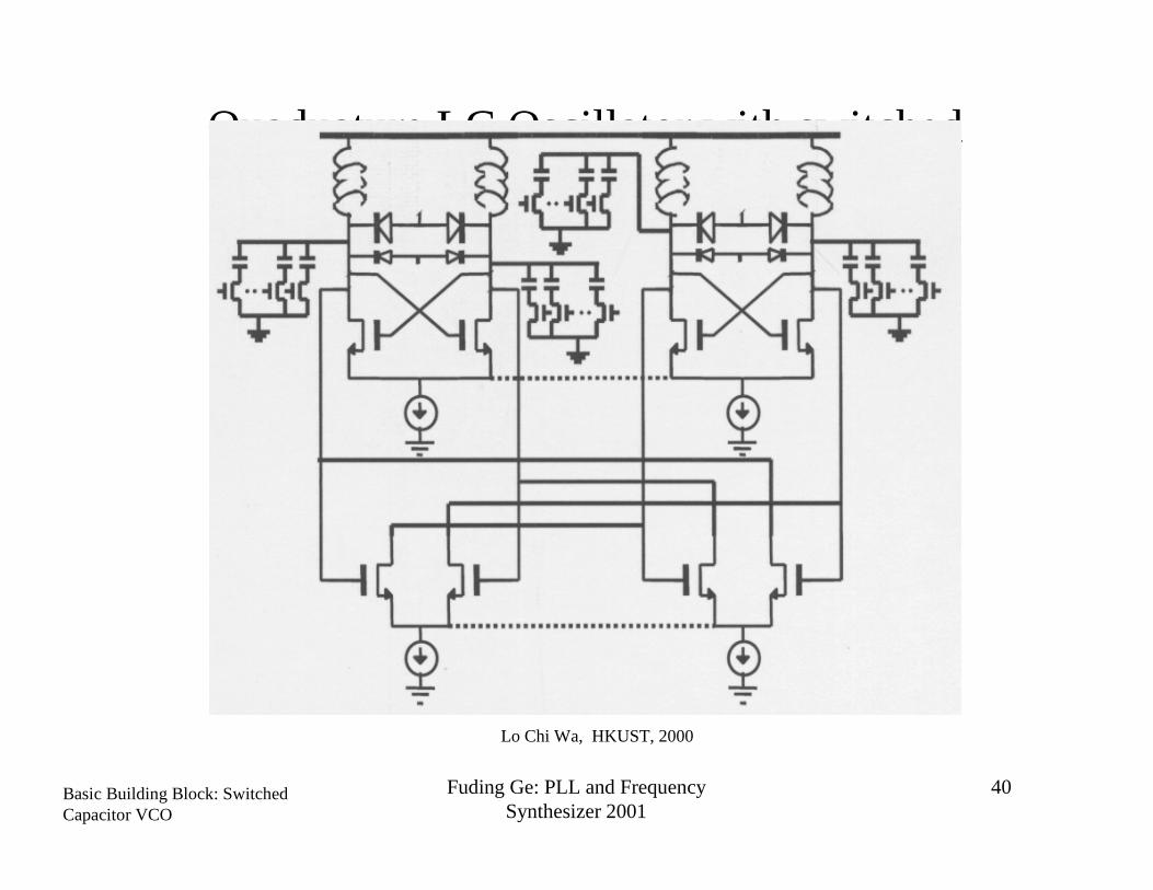
Quaduature LC Oscillator with switchedcapacitor array
Lo Chi Wa, HKUST, 2000
Basic Building Block: SwitchedCapacitor VCO
Fuding Ge: PLL and FrequencySynthesizer 2001
41
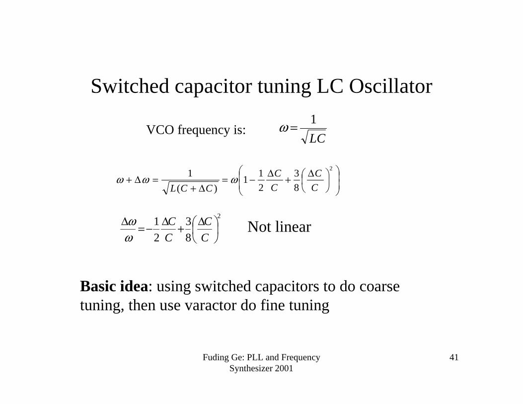
Switched capacitor tuning LC Oscillator
Basic idea: using switched capacitors to do coarsetuning, then use varactor do fine tuning
LC
1=ω
∆+∆−=
∆+=∆+
2
8
3
2
11
)(
1
C
C
C
C
CCLωωω
2
8
3
2
1
∆+∆−=∆
C
C
C
C
ωω Not linear
VCO frequency is:
Fuding Ge: PLL and FrequencySynthesizer 2001
42
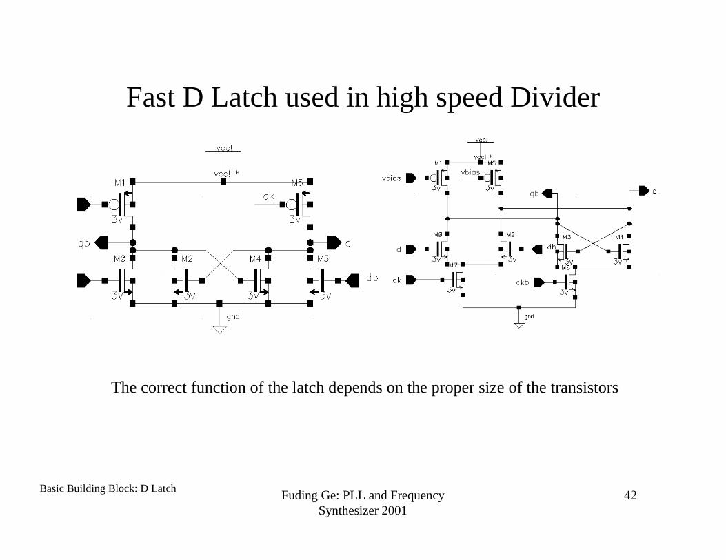
Fast D Latch used in high speed Divider
Basic Building Block: D Latch
The correct function of the latch depends on the proper size of the transistors
Fuding Ge: PLL and FrequencySynthesizer 2001
43
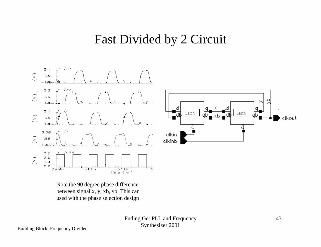
Fast Divided by 2 Circuit
Building Block: Frequency Divider
Note the 90 degree phase differencebetween signal x, y, xb, yb. This canused with the phase selection design
LatchLatch
Fuding Ge: PLL and FrequencySynthesizer 2001
44
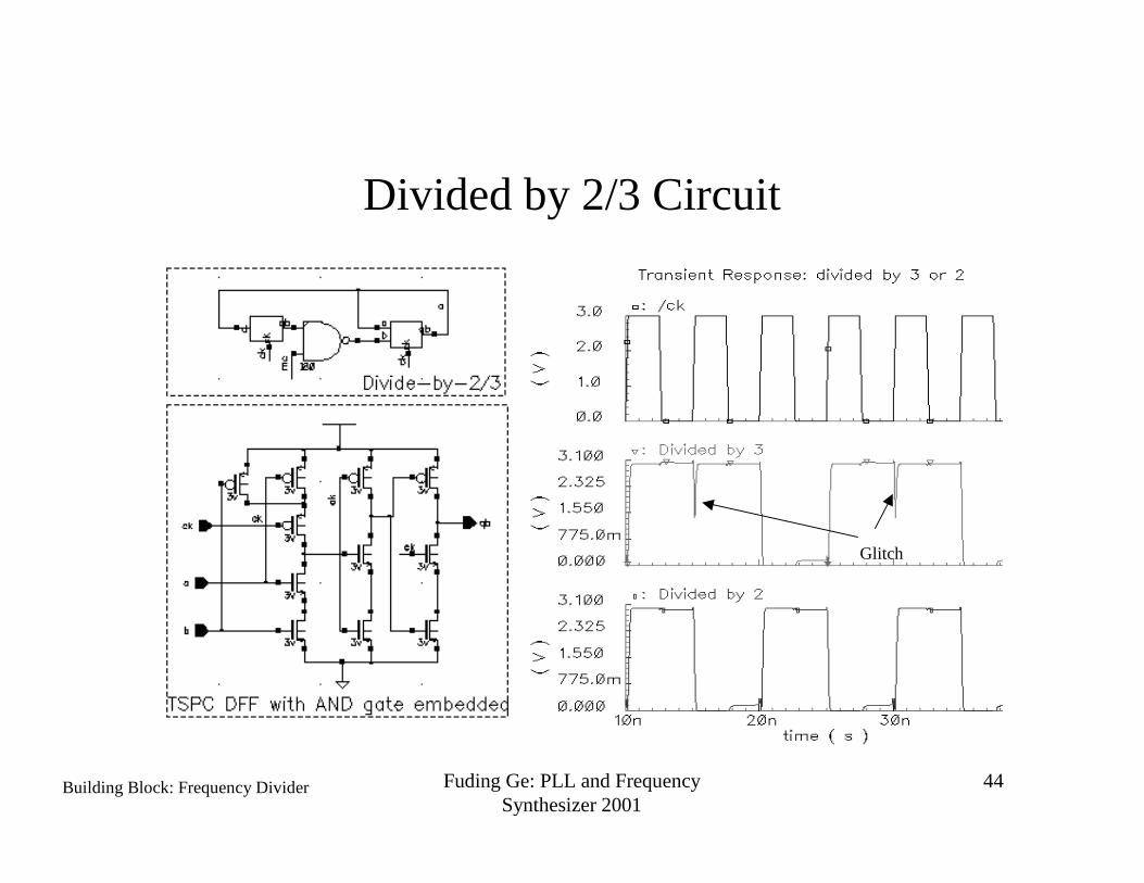
Divided by 2/3 Circuit
Glitch
Building Block: Frequency Divider
Fuding Ge: PLL and FrequencySynthesizer 2001
45
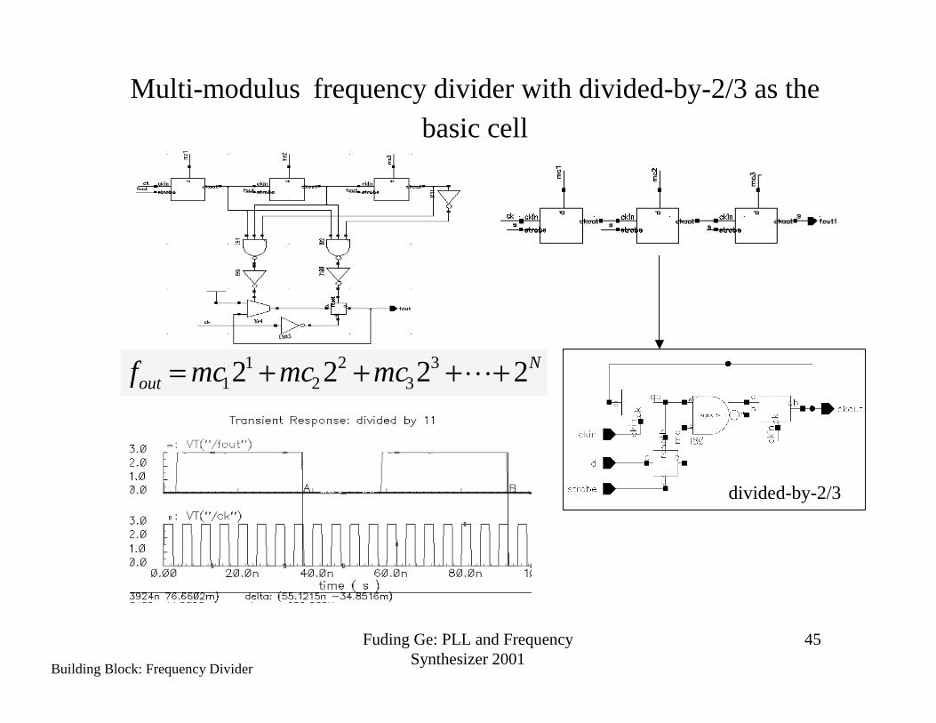
Multi-modulus frequency divider with divided-by-2/3 as thebasic cell
Nout mcmcmcf 2222 3
32
21
1 ++++= L
divided-by-2/3
Building Block: Frequency Divider
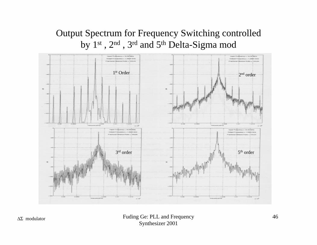
Fuding Ge: PLL and FrequencySynthesizer 2001
46
Output Spectrum for Frequency Switching controlledby 1st , 2nd , 3rd and 5th Delta-Sigma mod
∆Σ modulator
1st Order 2nd order
3rd order 5th order
Fuding Ge: PLL and FrequencySynthesizer 2001
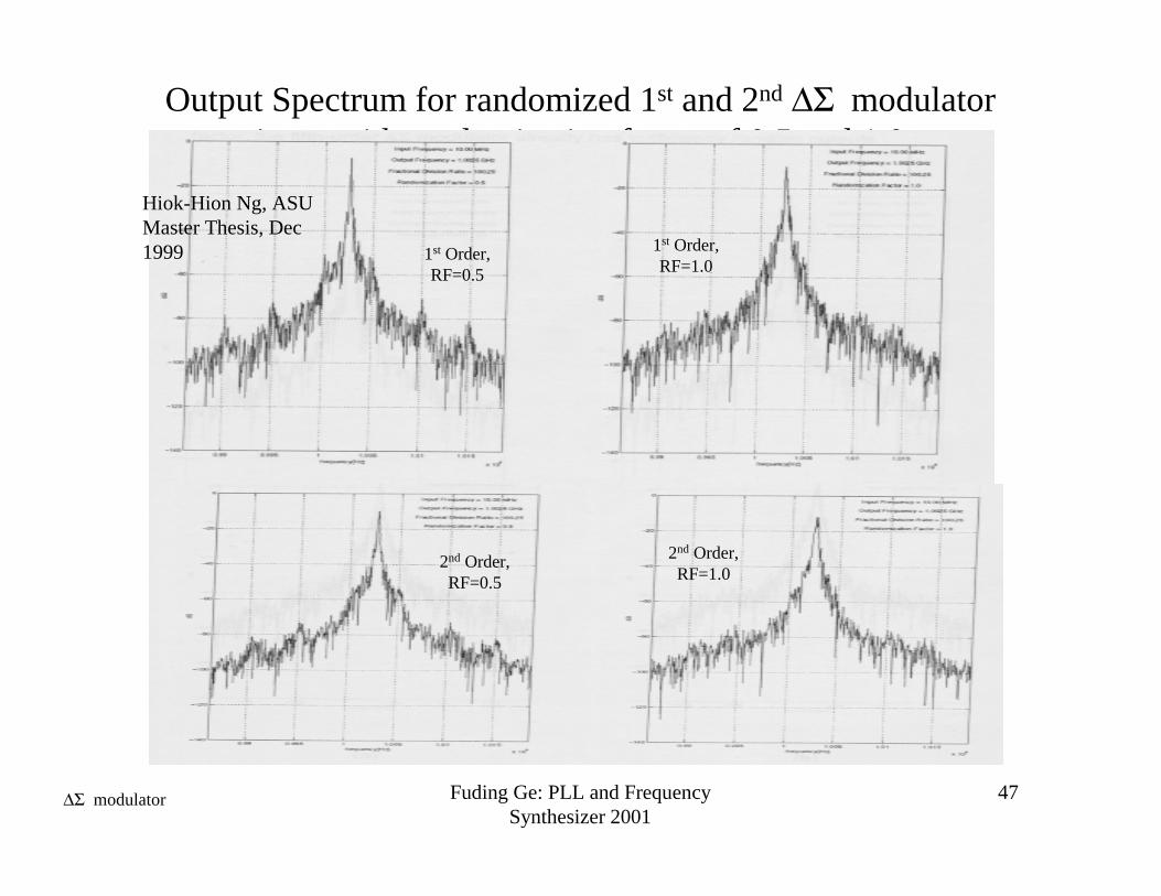
47
Output Spectrum for randomized 1st and 2nd ∆Σ modulatorinput with randomization factor of 0.5 and 1.0
Hiok-Hion Ng, ASUMaster Thesis, Dec1999 1st Order,
RF=0.5
1st Order,RF=1.0
2nd Order,RF=0.5
2nd Order,RF=1.0
∆Σ modulator
Fuding Ge: PLL and FrequencySynthesizer 2001
48
Order of Delta-Sigma Modulator
• Modulator Order (MO)↑:
SNR at LF ↑,
LPF order (FO)↑, FO = MO+1
Circuit Complexity ↑• Research shows: 3rd order is good enough
– Require: 23=8 modulus (3 bits) for MMD
– Require 4th order loop filter
• Research shows 24-bit accumulator provided resulting inenough accuracy
Mucahit Kozak et al: IMTC 2000
∆Σ modulator

Fuding Ge: PLL and FrequencySynthesizer 2001
49
∆Σ Modulator Architecture
• Interpolative• Instability
• MASH (MultistAge noise SHaping)• Cascade of low order ∆Σ Modulator
• Stable
• Can easily be implemented using pipeline structure
• Multibit output requires multi modulus divider– Example: MASH-3: 3 bits output, ⇒ 8 MMD
∆Σ modulator
Fuding Ge: PLL and FrequencySynthesizer 2001
50
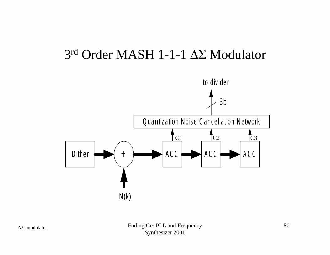
3rd Order MASH 1-1-1 ∆Σ Modulator
Dither +
N(k)
ACC ACC ACC
Quantization Noise Cancellation Network
3b
to divider
C1 C2 C3
∆Σ modulator
Fuding Ge: PLL and FrequencySynthesizer 2001
51
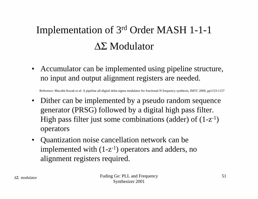
Implementation of 3rd Order MASH 1-1-1
∆Σ Modulator
• Accumulator can be implemented using pipeline structure,no input and output alignment registers are needed.
Reference: Mucahit Kozak et al: A pipeline all-digital delta-sigma modulator for fractional-N frequency synthesis, IMTC 2000, pp1153-1157
• Dither can be implemented by a pseudo random sequencegenerator (PRSG) followed by a digital high pass filter.High pass filter just some combinations (adder) of (1-z-1)operators
• Quantization noise cancellation network can beimplemented with (1-z-1) operators and adders, noalignment registers required.
∆Σ modulator
Fuding Ge: PLL and FrequencySynthesizer 2001
52
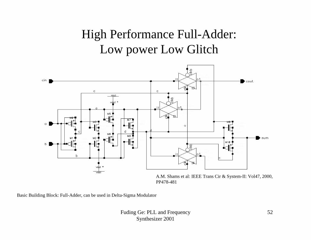
High Performance Full-Adder:Low power Low Glitch
Basic Building Block: Full-Adder, can be used in Delta-Sigma Modulator
A.M. Shams et al: IEEE Trans Cir & System-II: Vol47, 2000,PP478-481
Fuding Ge: PLL and FrequencySynthesizer 2001
53
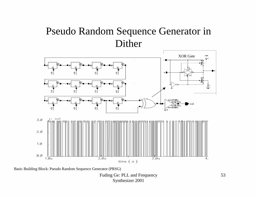
Pseudo Random Sequence Generator inDither
XOR Gate
Basic Building Block: Pseudo Random Sequence Generator (PRSG)
Fuding Ge: PLL and FrequencySynthesizer 2001
54
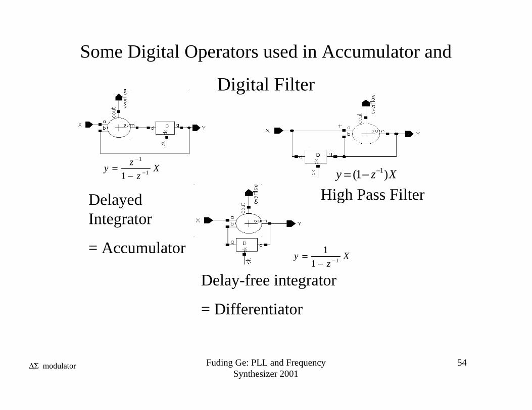
Some Digital Operators used in Accumulator and
Digital Filter
Xz
zy
1
1
1 −
−
−=
DelayedIntegrator
= AccumulatorX
zy
11
1−−
=
Delay-free integrator
= Differentiator
Xzy )1( 1−−=
High Pass Filter
∆Σ modulator
Fuding Ge: PLL and FrequencySynthesizer 2001
55
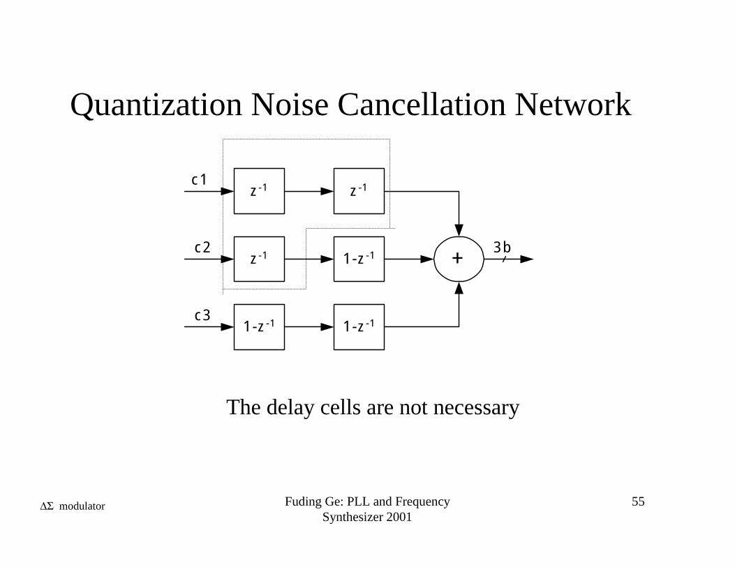
Quantization Noise Cancellation Network
The delay cells are not necessary
z-1 z-1
z-1 1-z-1
1-z-1 1-z-1
+3b
c1
c2
c3
∆Σ modulator
Fuding Ge: PLL and FrequencySynthesizer 2001
56
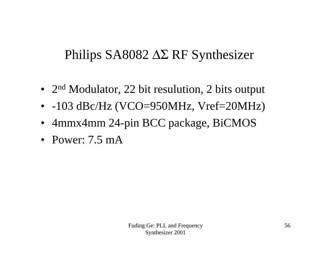
Philips SA8082 ∆Σ RF Synthesizer
• 2nd Modulator, 22 bit resulution, 2 bits output
• -103 dBc/Hz (VCO=950MHz, Vref=20MHz)
• 4mmx4mm 24-pin BCC package, BiCMOS
• Power: 7.5 mA