First Time, Every Time – Practical Tips for Phase- Locked ... · •Basic Feedback Loop Theory...
109
Copyright, Dennis Fischette, 2007 1 First Time, Every Time First Time, Every Time – – Practical Tips for Phase Practical Tips for Phase - - Locked Loop Design Locked Loop Design Dennis Fischette Email: [email protected] Website: http://www.delroy.com
-
Upload
truonghuong -
Category
Documents
-
view
219 -
download
0
Transcript of First Time, Every Time – Practical Tips for Phase- Locked ... · •Basic Feedback Loop Theory...
Copyright, Dennis Fischette, 2007
1
First Time, Every Time First Time, Every Time ––Practical Tips for PhasePractical Tips for Phase--
Locked Loop DesignLocked Loop Design
Dennis FischetteEmail: [email protected]
Website: http://www.delroy.com
Copyright, Dennis Fischette, 2007
2
OutlineOutline
• Introduction• Basic Feedback Loop Theory• Jitter and Phase Noise• Common Circuit Implementations• Circuit Verification• Design for Test
Copyright, Dennis Fischette, 2007
3
IntroductionIntroduction
Copyright, Dennis Fischette, 2007
4
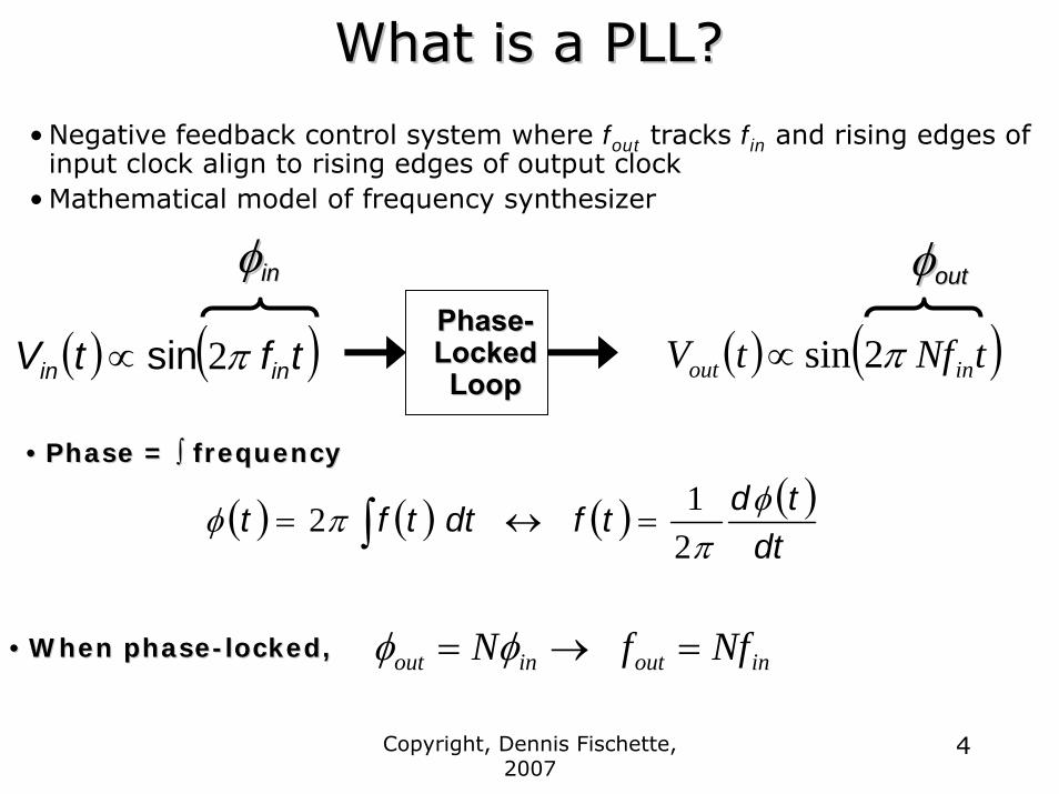
What is a PLL?What is a PLL?
• Negative feedback control system where fout tracks fin and rising edges of input clock align to rising edges of output clock
• Mathematical model of frequency synthesizer
( ) ( )tftV inin π2sin∝ ( ) ( )tNftV inout π2sin∝
φφoutoutφφinin
( ) ( ) ( ) ( )dt
tdtfdttft φπ
πφ212 =↔= ∫
PhasePhase--LockedLockedLoopLoop
inoutinout NffN =→= φφ•• When phaseWhen phase--locked,locked,
•• Phase = Phase = ∫∫ frequencyfrequency

Copyright, Dennis Fischette, 2007
5
ChargeCharge--Pump PLL Block DiagramPump PLL Block Diagram
• Sampled-system (phase-error is input variable)• Phase error is corrected by changing frequency (φ(t) = ∫ f(t) dt)• Resistor provides means to separate correction of frequency error
from correction of phase error
ClkOutPhase-Freq
Detector
ChargePump
FeedbackDiv
VCORefClk Level-
Shifter
FbClk
GoFaster
GoSlower
VCO
Vctl
C1 C2
Copyright, Dennis Fischette, 2007
6
PLL Feedback Loop TheoryPLL Feedback Loop Theory
Copyright, Dennis Fischette, 2007
7
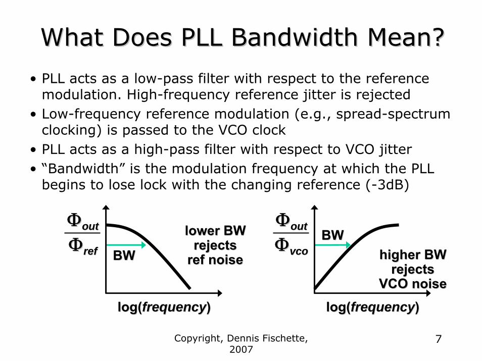
What Does PLL Bandwidth Mean?What Does PLL Bandwidth Mean?
• PLL acts as a low-pass filter with respect to the reference modulation. High-frequency reference jitter is rejected
• Low-frequency reference modulation (e.g., spread-spectrum clocking) is passed to the VCO clock
• PLL acts as a high-pass filter with respect to VCO jitter• “Bandwidth” is the modulation frequency at which the PLL
begins to lose lock with the changing reference (-3dB)
log(log(frequencyfrequency))
BWBW
ΦΦoutout
ΦΦrefref
lower BW lower BW rejectsrejects
ref noiseref noise
log(log(frequencyfrequency))
BWBWΦΦoutout
ΦΦvcovco higher BW higher BW rejectsrejects
VCO noiseVCO noise
Copyright, Dennis Fischette, 2007
8
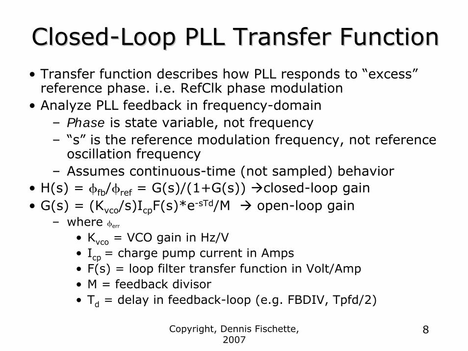
ClosedClosed--Loop PLL Transfer FunctionLoop PLL Transfer Function• Transfer function describes how PLL responds to “excess”
reference phase. i.e. RefClk phase modulation• Analyze PLL feedback in frequency-domain
– Phase is state variable, not frequency– “s” is the reference modulation frequency, not reference
oscillation frequency– Assumes continuous-time (not sampled) behavior
• H(s) = φfb/φref = G(s)/(1+G(s)) closed-loop gain• G(s) = (Kvco/s)IcpF(s)*e-sTd/M open-loop gain
– where φerr
• Kvco = VCO gain in Hz/V• Icp = charge pump current in Amps• F(s) = loop filter transfer function in Volt/Amp• M = feedback divisor• Td = delay in feedback-loop (e.g. FBDIV, Tpfd/2)
Copyright, Dennis Fischette, 2007
9
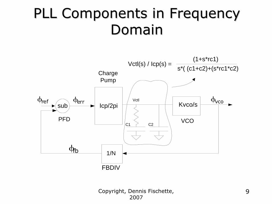
PLL Components in Frequency PLL Components in Frequency DomainDomain
PFD
Icp/2pi
VCO
Vctl
C1 C2
1/N
Kvco/s
FBDIV
ChargePump
sub
s*( (c1+c2)+(s*rc1*c2)(1+s*rc1)
Vctl(s) / Icp(s) =
φvcoφref
φfb
φerr
Copyright, Dennis Fischette, 2007
10
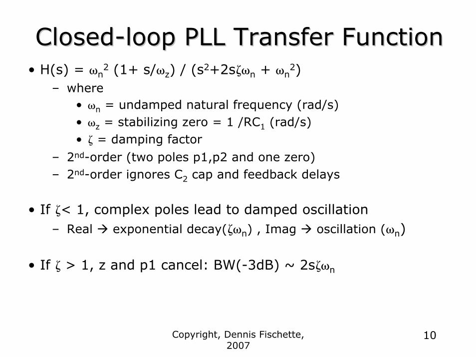
ClosedClosed--loop PLL Transfer Functionloop PLL Transfer Function• H(s) = ωn
2 (1+ s/ωz) / (s2+2sζωn + ωn2)
– where• ωn = undamped natural frequency (rad/s)• ωz = stabilizing zero = 1 /RC1 (rad/s)• ζ = damping factor
– 2nd-order (two poles p1,p2 and one zero)– 2nd-order ignores C2 cap and feedback delays
• If ζ< 1, complex poles lead to damped oscillation– Real exponential decay(ζωn) , Imag oscillation (ωn)
• If ζ > 1, z and p1 cancel: BW(-3dB) ~ 2sζωn
Copyright, Dennis Fischette, 2007
11
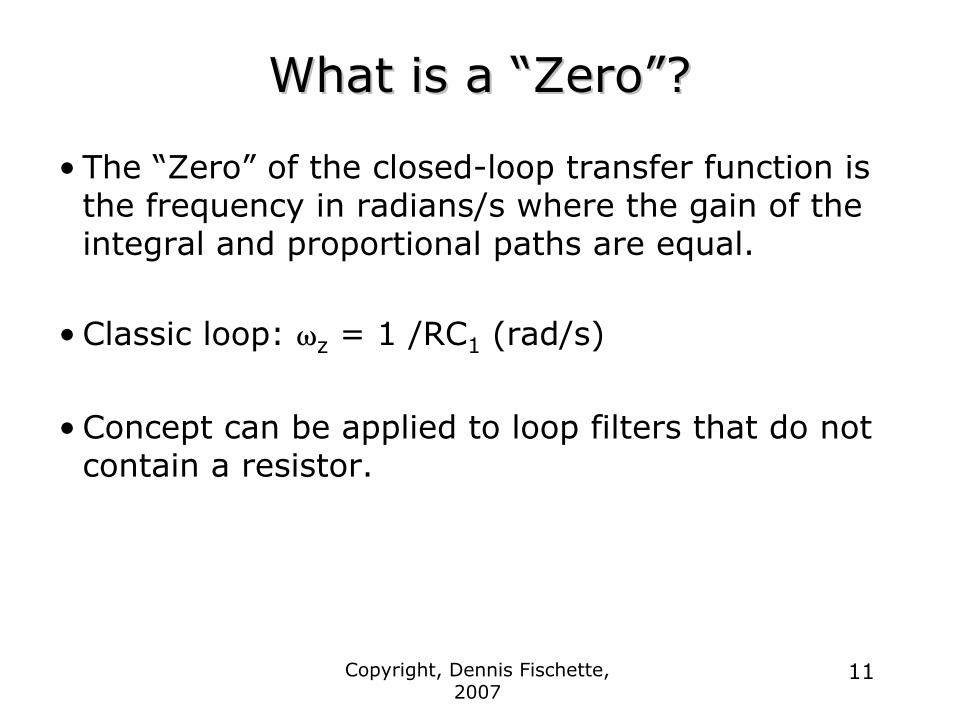
What is a What is a ““ZeroZero””??
• The “Zero” of the closed-loop transfer function is the frequency in radians/s where the gain of the integral and proportional paths are equal.
• Classic loop: ωz = 1 /RC1 (rad/s)
• Concept can be applied to loop filters that do not contain a resistor.
Copyright, Dennis Fischette, 2007
12
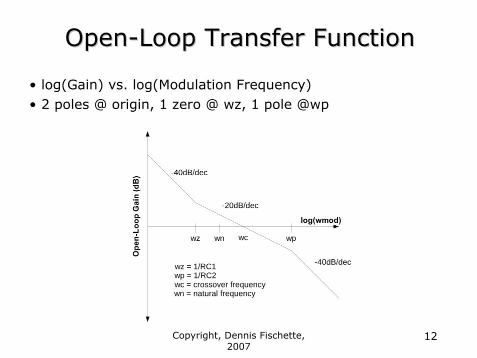
OpenOpen--Loop Transfer FunctionLoop Transfer Function
• log(Gain) vs. log(Modulation Frequency)• 2 poles @ origin, 1 zero @ wz, 1 pole @wp
log(wmod)
Ope
n-Lo
op G
ain
(dB
)
-40dB/dec
-20dB/dec
-40dB/dec
wz wc wpwn
wz = 1/RC1wp = 1/RC2wc = crossover frequencywn = natural frequency
Copyright, Dennis Fischette, 2007
13
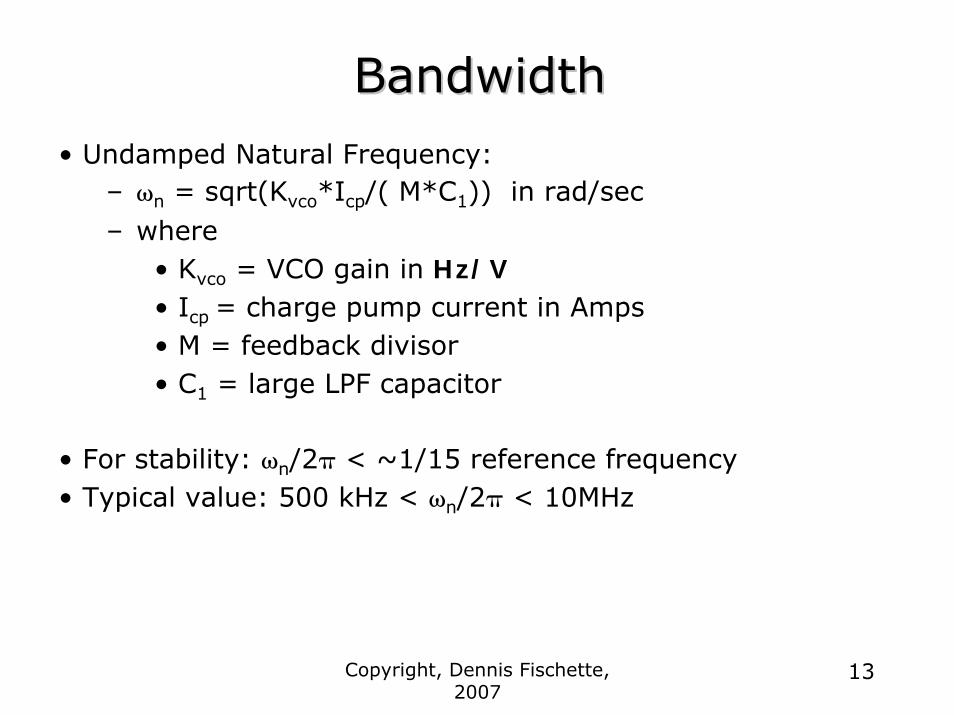
BandwidthBandwidth• Undamped Natural Frequency:
– ωn = sqrt(Kvco*Icp/( M*C1)) in rad/sec– where
• Kvco = VCO gain in Hz/V• Icp = charge pump current in Amps• M = feedback divisor• C1 = large LPF capacitor
• For stability: ωn/2π < ~1/15 reference frequency • Typical value: 500 kHz < ωn/2π < 10MHz

Copyright, Dennis Fischette, 2007
14
Stability, Damping, and Phase MarginStability, Damping, and Phase Margin• Damping Factor: ζ = Rlpf * C1 * ωn /2
– Dimensionless, Usually ~0.45 < ζ < ~2– Lower end of range for low period jitter– Higher end of range for accurate ref phase tracking– Rlpf provides means to set stability independent of bandwidth
• φm (degrees) = (180/π)*(atan(ωc*RC1)–atan(ωc*RC2)-ωc*Tdly)– ωc == crossover frequency
• frequency where open-loop gain G(s) = 0dB– For stability: 1/RC1 (zero) < ωc < 1/RC2 (parasitic pole)– Typical Range: 1.2*ωn < ωc < 2.5*ωn
• Phase margin degradation due to PFD phase error sampling– -φ = ωc*Tref / 2– z-domain analysis is more accurate
• Phase margin (φm) ~ 100 * ζ (for ζ < 0.5)– Usually 45° < PM < 70°
Copyright, Dennis Fischette, 2007
15
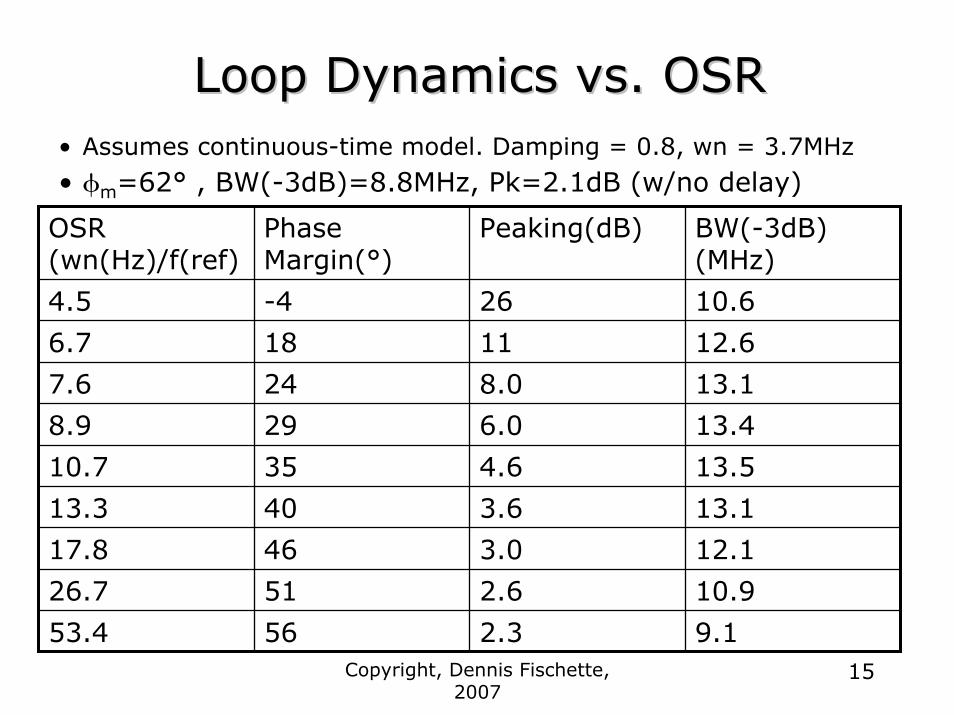
Loop Dynamics vs. OSRLoop Dynamics vs. OSR• Assumes continuous-time model. Damping = 0.8, wn = 3.7MHz
• φm=62° , BW(-3dB)=8.8MHz, Pk=2.1dB (w/no delay)
OSR (wn(Hz)/f(ref)
Phase Margin(°)
Peaking(dB) BW(-3dB) (MHz)
4.5 -4 26 10.6
6.7 18 11 12.6
7.6 24 8.0 13.1
8.9 29 6.0 13.4
10.7 35 4.6 13.5
13.3 40 3.6 13.1
17.8 46 3.0 12.1
26.7 51 2.6 10.9
53.4 56 2.3 9.1
Copyright, Dennis Fischette, 2007
16
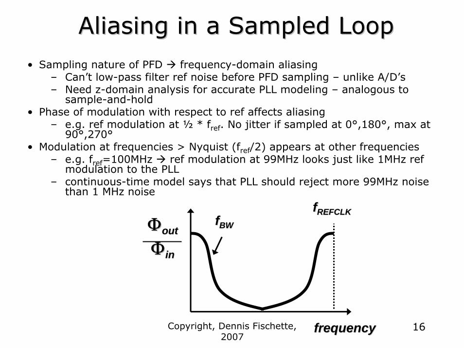
Aliasing in a Sampled LoopAliasing in a Sampled Loop• Sampling nature of PFD frequency-domain aliasing
– Can’t low-pass filter ref noise before PFD sampling – unlike A/D’s– Need z-domain analysis for accurate PLL modeling – analogous to
sample-and-hold• Phase of modulation with respect to ref affects aliasing
– e.g. ref modulation at ½ * fref. No jitter if sampled at 0°,180°, max at 90°,270°
• Modulation at frequencies > Nyquist (fref/2) appears at other frequencies– e.g. fref=100MHz ref modulation at 99MHz looks just like 1MHz ref
modulation to the PLL– continuous-time model says that PLL should reject more 99MHz noise
than 1 MHz noise
frequencyfrequency
ffREFCLKREFCLKffBWBWΦΦoutout
ΦΦinin
Copyright, Dennis Fischette, 2007
17
PLL Response vs. DampingPLL Response vs. Damping
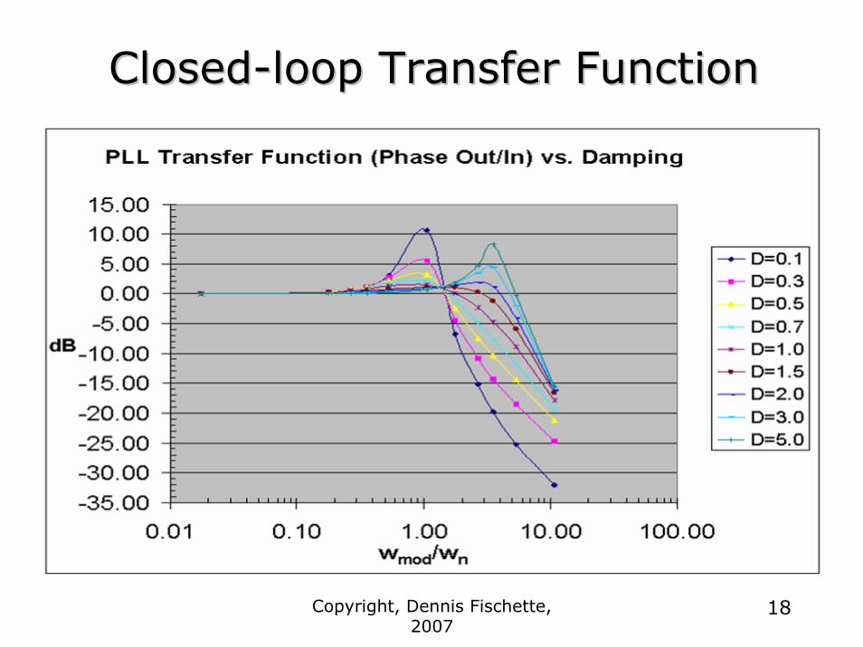
Copyright, Dennis Fischette, 2007
18
ClosedClosed--loop Transfer Functionloop Transfer Function
Copyright, Dennis Fischette, 2007
19
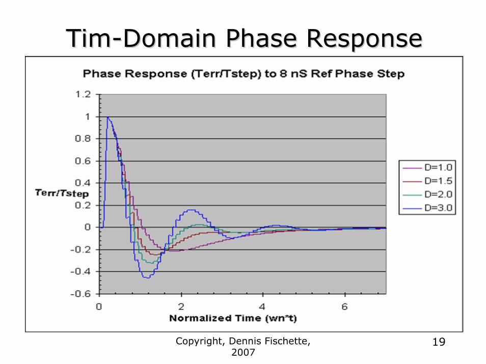
TimTim--Domain Phase ResponseDomain Phase Response
Copyright, Dennis Fischette, 2007
20
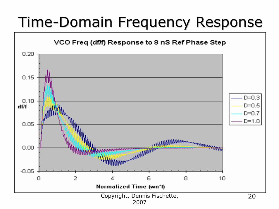
TimeTime--Domain Frequency ResponseDomain Frequency Response
Copyright, Dennis Fischette, 2007
21
Jitter and Phase NoiseJitter and Phase Noise
Copyright, Dennis Fischette, 2007
22
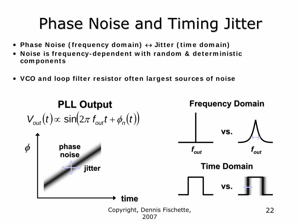
Phase Noise and Timing JitterPhase Noise and Timing Jitter• Phase Noise (frequency domain) ↔ Jitter (time domain)• Noise is frequency-dependent with random & deterministic
components
• VCO and loop filter resistor often largest sources of noise
timetime
φφ
( ) ( )( )ttftV noutout φπ +∝ 2sinFrequency DomainFrequency Domain
Time DomainTime Domain
phasephasenoisenoise
jitterjitter
vs.vs.
vs.vs.
PLL OutputPLL Output
ffoutout ffoutout
Copyright, Dennis Fischette, 2007
23
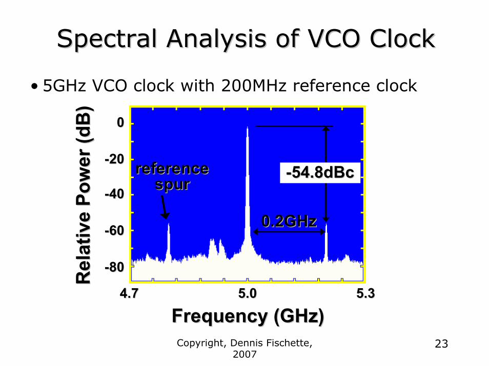
Spectral Analysis of VCO ClockSpectral Analysis of VCO Clock
• 5GHz VCO clock with 200MHz reference clock
5.05.04.74.7 5.35.3
00
--2020
--4040
--6060
--8080
Rel
ativ
e Po
wer
(dB
)R
elat
ive
Pow
er (d
B)
Frequency (GHz)Frequency (GHz)
--54.8dBc54.8dBcreferencereferencespurspur
0.2GHz0.2GHz
Copyright, Dennis Fischette, 2007
24
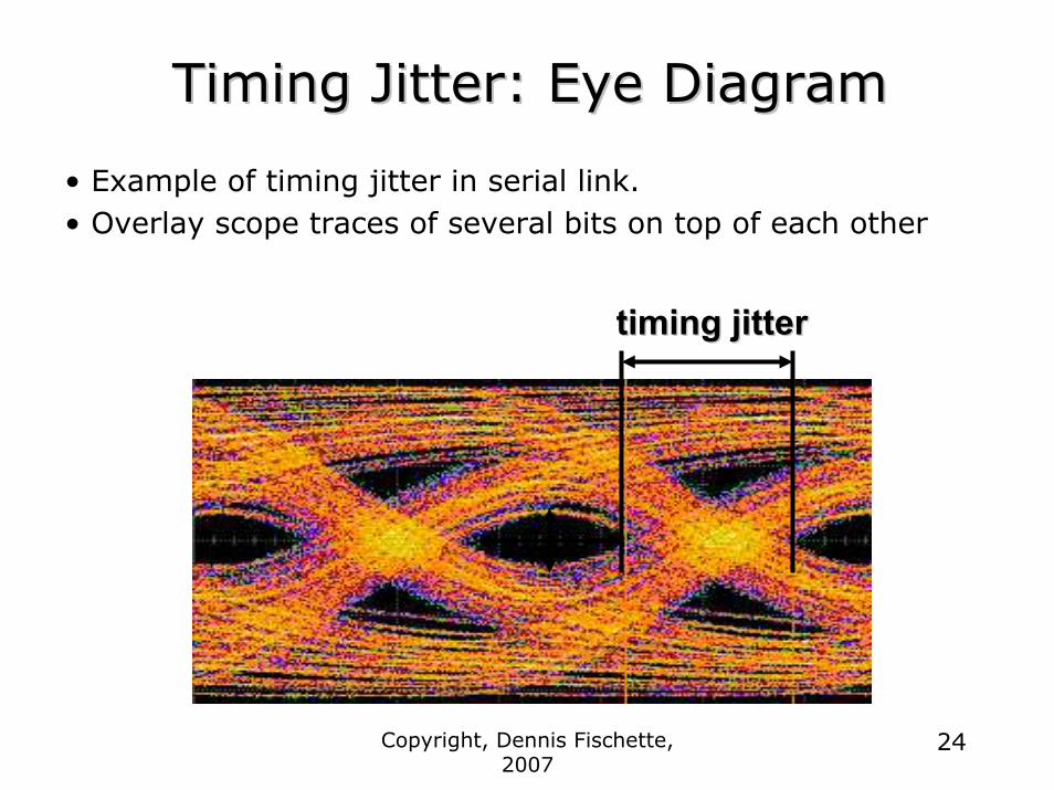
Timing Jitter: Eye DiagramTiming Jitter: Eye Diagram
• Example of timing jitter in serial link.• Overlay scope traces of several bits on top of each other
timing jittertiming jitter
Copyright, Dennis Fischette, 2007
25
Jitter DefinitionsJitter Definitions
• Phase Jitter (sec) – deviation of VCO output edges from ideal placement in time. – specified over a time interval or frequency range.– important for I/O apps (e.g. PCI-Express < ±1.5ps RMS)– measure with spectrum analyzer or scope with jitter package
• Period Jitter (sec)– deviation of VCO period from ideal period– derivative of Phase Jitter with respect to time– peak-to-peak period jitter (Jpp) is max VCO period – min VCO period– most important for CPU-like apps– e.g. 10-20ps for 2GHz CPU clock– easily measured on scope – self-triggered infinite-persistence or jitter
package
• Cycle-to-Cycle Jitter (sec)– change in VCO period from cycle N to cycle N+1– derivative of Period Jitter with respect to time– not important for CPU-like apps
Copyright, Dennis Fischette, 2007
26
Jitter DefinitionsJitter Definitions
• TIE (sec)– time difference between total of N-consecutive actual VCO cycles and
N ideal cycles– easily measured on oscilloscope with jitter package – self-triggered
measurement
Copyright, Dennis Fischette, 2007
27
Noise SourcesNoise Sources• Major internal PLL Noise Sources
– charge-pump (flicker (1/f) and thermal) – loop filter resistor (thermal) – very significant– VCO (mostly thermal) - significant– VCO bias (flicker and thermal) – most significant– Flicker Noise
• Vn2 (V2/Hz) = Kf / (Cox*W*L* f)
• Kf ~ 10e-24
– Thermal Noise• In
2 (Amp2/Hz) = 4kT*gm*γγ ~ 2/3 for older CMOS technologies, much higher in deep submicron
• PLL feedback loop– Low-pass filters ref and charge-pump noise– Band-pass filters loop-filter resistor noise– High-pass filters VCO noise
Copyright, Dennis Fischette, 2007
28
Output Phase NoiseOutput Phase Noise
• Measured vs. offset frequency (f) from carrier
• Spectral Density of Phase Fluctuations (Sφ(f))– Sφ(f)= 2L(f)
• L(f) is Single-Sideband Phase Noise– Analogous to Power(sideband)/Power(carrier)– Sφ (f) is specified in a 1Hz band
• Sφ(f) ~ 1 / f2 (thermal region, mid-to-high f) (open-loop)• Sφ(f) ~ 1 / f3 (flicker region, low f) (open-loop)
• Flicker noise mostly filtered by high BW PLL
Copyright, Dennis Fischette, 2007
29
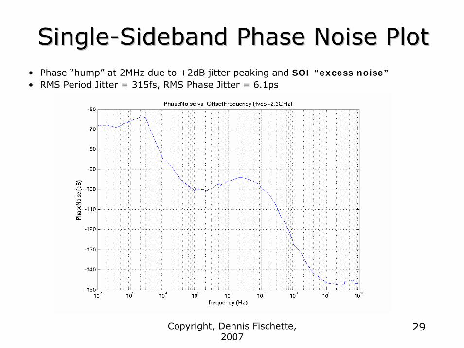
SingleSingle--Sideband Phase Noise PlotSideband Phase Noise Plot• Phase “hump” at 2MHz due to +2dB jitter peaking and SOI “excess noise”• RMS Period Jitter = 315fs, RMS Phase Jitter = 6.1ps
Copyright, Dennis Fischette, 2007
30
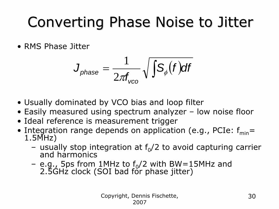
Converting Phase Noise to JitterConverting Phase Noise to Jitter
• RMS Phase Jitter
• Usually dominated by VCO bias and loop filter• Easily measured using spectrum analyzer – low noise floor• Ideal reference is measurement trigger• Integration range depends on application (e.g., PCIe: fmin=
1.5MHz)– usually stop integration at f0/2 to avoid capturing carrier
and harmonics– e.g., 5ps from 1MHz to f0/2 with BW=15MHz and
2.5GHz clock (SOI bad for phase jitter)
( )dffSf
Jvco
phase ∫= φπ21
Copyright, Dennis Fischette, 2007
31
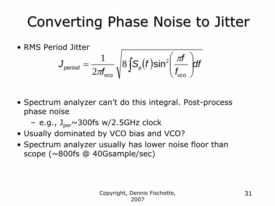
Converting Phase Noise to JitterConverting Phase Noise to Jitter
• RMS Period Jitter
• Spectrum analyzer can’t do this integral. Post-process phase noise
– e.g., Jper~300fs w/2.5GHz clock• Usually dominated by VCO bias and VCO?• Spectrum analyzer usually has lower noise floor than
scope (~800fs @ 40Gsample/sec)
( ) dff
ffSf
Jvcovco
period ⎟⎟⎠
⎞⎜⎜⎝
⎛= ∫
ππ φ
282
1 sin
Copyright, Dennis Fischette, 2007
32
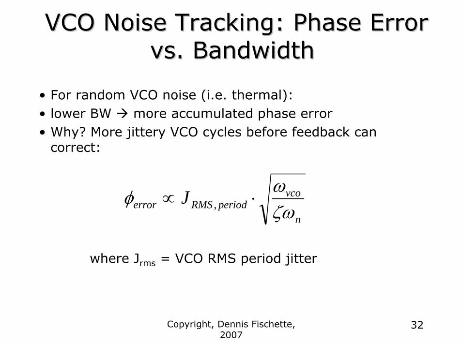
VCO Noise Tracking: Phase Error VCO Noise Tracking: Phase Error vs. Bandwidthvs. Bandwidth
• For random VCO noise (i.e. thermal): • lower BW more accumulated phase error• Why? More jittery VCO cycles before feedback can
correct:
where Jrms = VCO RMS period jitter
n
vcoperiodRMSerror J
ζωωφ ⋅∝ ,
Copyright, Dennis Fischette, 2007
33
PLL CircuitsPLL Circuits
• Phase-Frequency Detector
• Charge-Pump
• Loop Filter
• Voltage-Controlled Oscillator
• Level-Shifter
• Feedback Divider
• Voltage Regulator
• Miscellaneous
Copyright, Dennis Fischette, 2007
34
PhasePhase--Frequency Frequency Detector(PFD)Detector(PFD)
Copyright, Dennis Fischette, 2007
35
PFD Block DiagramPFD Block Diagram• Edge-triggered - input duty-cycle doesn’t matter - frequency
correction takes precedence over phase correction – no harmonic locking – 3 state operation
• Output pulse-widths proportional to phase error• Delay to remove “dead-zone”• Symmetric NAND used to balance equalize delays from both inputs
G oFaste rD
C K
Q
D FF
D LY
G oS low er
R ef
V dd
V dd
FB
D
C K
Q
D FF
Q
C K
D
R
R
Copyright, Dennis Fischette, 2007
36
Example: PFDExample: PFD
Ref
FbClk
GoFaster
GoSlower
Vctl
Cycle Slip
Copyright, Dennis Fischette, 2007
37
Frequency Lock DetectorFrequency Lock Detector
• Sample PFD GoFaster signal with rising REFCLK
• Sample PFD GoSlower signal with rising FBCLK
• If either sampled signal is TRUE, then PFD detected two consecutive REFCLK’s or FBCLK’s cycle slip and loss of frequency lock
• May apply “sticky bit” to result to capture temporary loss of lock
Copyright, Dennis Fischette, 2007
38
Charge Pump(CP)Charge Pump(CP)
Copyright, Dennis Fischette, 2007
39
ChargeCharge--Pump Wish ListPump Wish List• Equal UP/DOWN currents over entire control voltage range -
reduce static phase error• Minimize mismatch caused by finite current sources gds and
Vt mismatches– ∆Vt ~ 1 / sqrt(W*L)– long L in current sources for higher gds
– Stacked (a.k.a common) gates in Isources help w/mismatch– use replica-bias CP and feedback amplifier to balance Iup/Idown
– beware of mismatch between two CP cells– increase in CP’s phase noise due to finite BW of this feedback?
• Minimal coupling to control voltage during switching and leakage when off - reduce jitter and phase drift
• Insensitive to power-supply noise and process variations –loop stability
Copyright, Dennis Fischette, 2007
40
ChargeCharge--Pump Wish ListPump Wish List
• Minimize coupling caused by “clock feedthrough” (Cgd) and charge-injection
– ½ sized dummy switches to reduce charge-injection • Qinj ~ ½ *Cox*(W*L)*(Vgs-Vt)
– Small (and/or limited swing) switches to reduce clock feedthrough – watch for leakage with limited-swing
– Balance timing and slew rates of all inputs
• Minimize PFD pulsewidth to minimize phase noise while still avoiding dead-zone (< 100 ps possible in 65nm)
• Typical Icp: 5µA (mismatch)< Icp < 50 µA (∆Vctl)
Copyright, Dennis Fischette, 2007
41
Static Phase Error and CP Static Phase Error and CP Up/Down MismatchesUp/Down Mismatches
• Static Phase Error: in lock, net UP and DOWN currents must integrate to zero
– If UP current is 2× larger, then DOWN current source must be on 2× as long to compensate
– Feedback clock must lead reference for DOWN to be on longer
– Terr = Tdn - Tup = Treset * (Iup/Idn – 1) • Narrow reset pulse generally lower static error• Typical static phase error < 100ps• Static phase error period jitter @ Tref (reference spurs)
Copyright, Dennis Fischette, 2007
42
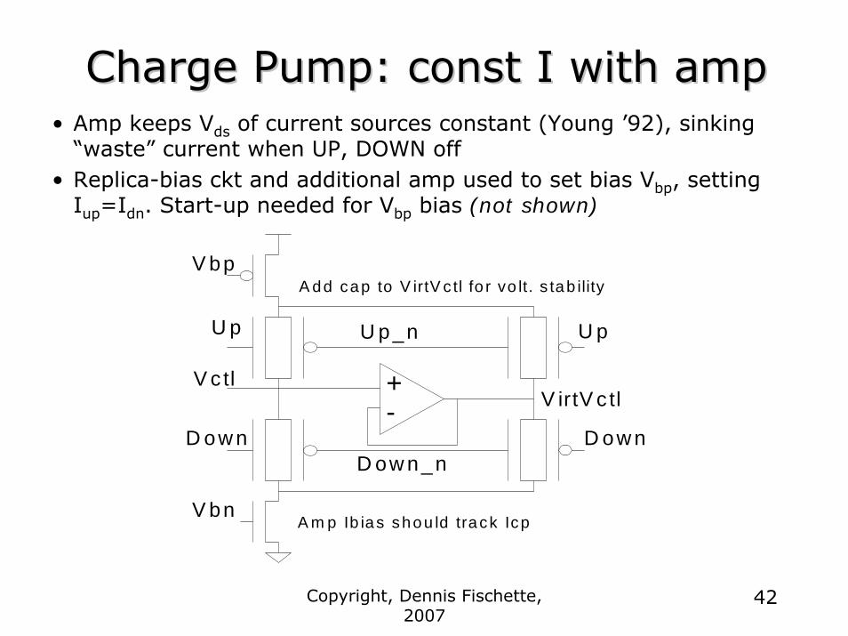
Charge Pump: const I with ampCharge Pump: const I with amp• Amp keeps Vds of current sources constant (Young ’92), sinking
“waste” current when UP, DOWN off• Replica-bias ckt and additional amp used to set bias Vbp, setting
Iup=Idn. Start-up needed for Vbp bias (not shown)
U p
D ow nD ow n
V ctl
V bn
V bp
+-
U p_n
D ow n_n
U p
V irtV c tl
A dd cap to V irtV c tl fo r vo lt. s tab ility
A m p Ib ias shou ld track Icp
Copyright, Dennis Fischette, 2007
43
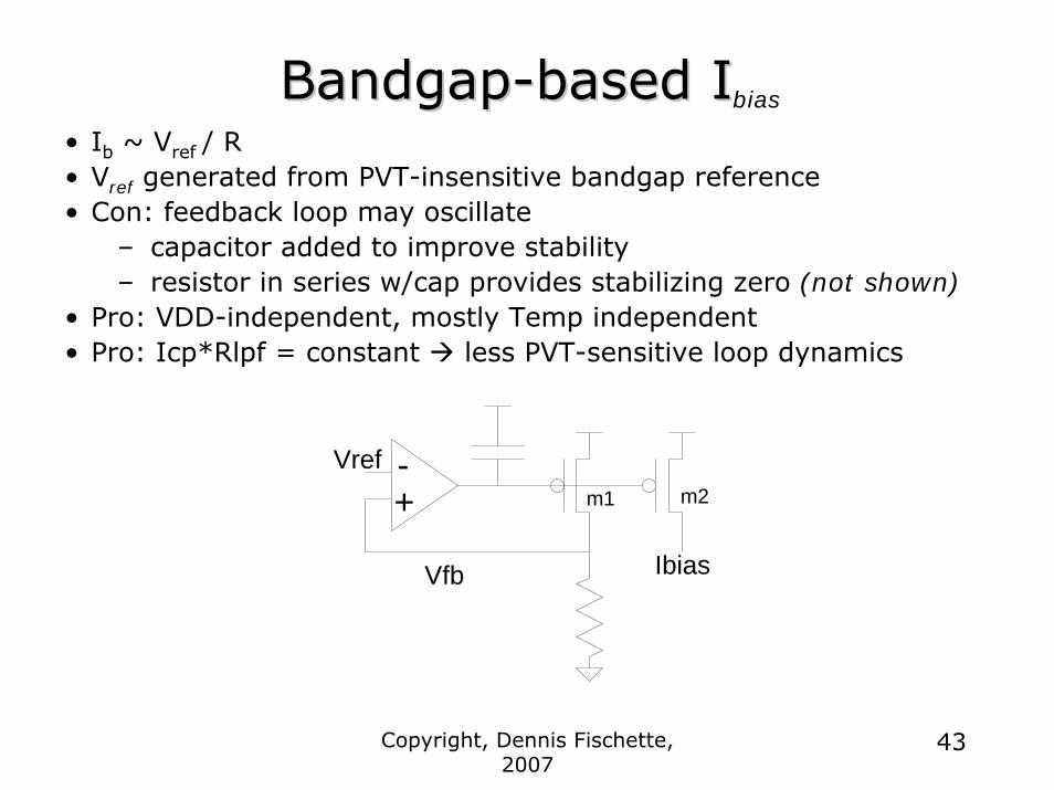
BandgapBandgap--based Ibased Ibias
• Ib ~ Vref / R• Vref generated from PVT-insensitive bandgap reference• Con: feedback loop may oscillate
– capacitor added to improve stability– resistor in series w/cap provides stabilizing zero (not shown)
• Pro: VDD-independent, mostly Temp independent• Pro: Icp*Rlpf = constant less PVT-sensitive loop dynamics
Ibias
Vref
Vfb
-+ m2m1
Copyright, Dennis Fischette, 2007
44
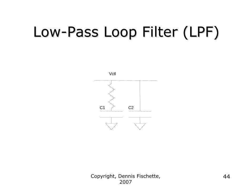
LowLow--Pass Loop Filter (LPF)Pass Loop Filter (LPF)
Vctl
C1 C2
Copyright, Dennis Fischette, 2007
45
Loop Filter BasicsLoop Filter Basics
• Simplest and most commonly-used loop filter is continuous-time, passive filter
• Filters high-frequency phase error information from PFD/CP while integrating low-frequency error info onto C1 cap to set avg. freq -affects bandwidth
• Provides a means of isolating phase correction from frequency correction – Icp*Rlpf – affects stability
• Filters noise spurs caused by sampling – C2 cap – adds parasitic pole at 1/RC2
• Other options include digital(FSM-based) filter, sampled-time filter (see Maneatis, Maxim) , and continuous-time active filter
• Differential designs can reduce sensitivity to VDD and substratenoise and often area by 2×. Requires common-mode feedback loop.
Copyright, Dennis Fischette, 2007
46
Passive, ContinuousPassive, Continuous--Time Loop FilterTime Loop Filter
• R may be programmable– Avoid gate leakage and noise coupling from switches and parasitic
resistance at extreme control voltages
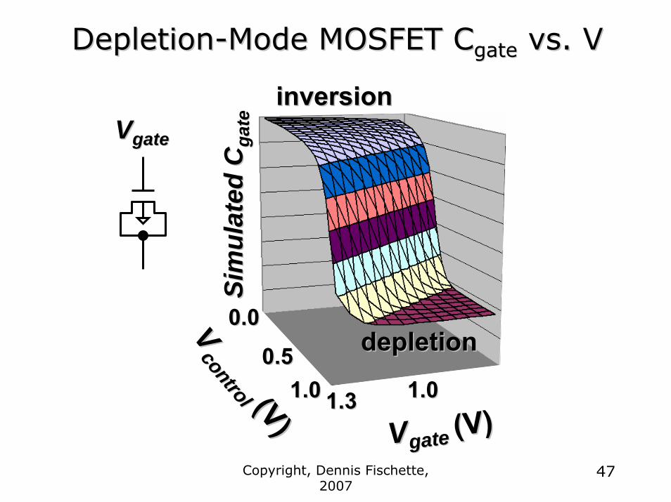
• Leakage in MOSFET caps may be a HUGE problem– Exponential I vs. V: Ileak~Vgate
4 (approximate)– Weak temperature dependence– Ileak vs. tox ~2-3× per Angström– Use metal caps (10× larger) or thick-gate oxide caps to minimize
leakage– If MOSFET caps, accumulation mode preferred – flatter Cgate vs. V
• Typical values:– 0.5kΩ < Rlpf < 20kΩ– 5pF < C1 < 200 pF– 2% (low phase error) < C2/C1 < 10% (low period jitter)– Smaller caps are becoming more common w/ higher reference
frequencies and metal cap usage
Copyright, Dennis Fischette, 2007
47
DepletionDepletion--Mode MOSFET CMode MOSFET Cgategate vs. Vvs. V
VVgategate
inversioninversion
depletiondepletion
1.01.01.31.31.01.0
0.00.0
VVgategate (V)(V)VV
control
control (V)(V)
Sim
ulat
ed
Sim
ulat
ed CC
gate
gate
0.50.5
Copyright, Dennis Fischette, 2007
48
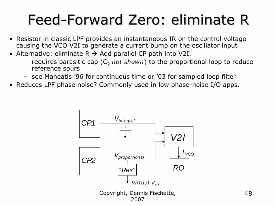
FeedFeed--Forward Zero: eliminate RForward Zero: eliminate R• Resistor in classic LPF provides an instantaneous IR on the control voltage
causing the VCO V2I to generate a current bump on the oscillator input• Alternative: eliminate R Add parallel CP path into V2I.
– requires parasitic cap (C2 not shown) to the proportional loop to reduce reference spurs
– see Maneatis ’96 for continuous time or ’03 for sampled loop filter• Reduces LPF phase noise? Commonly used in low phase-noise I/O apps.
CP1Vintegral
Virtual Vctl
CP2“Res”
Vproportional
V2I
RO
IVCO
Copyright, Dennis Fischette, 2007
49
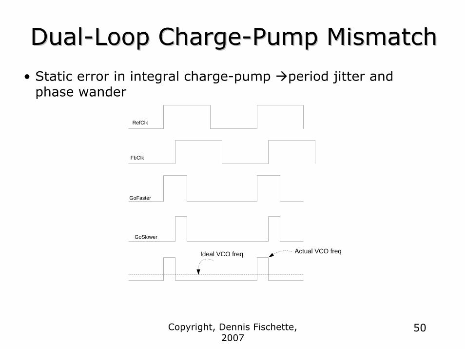
DualDual--Loop ChargeLoop Charge--Pump MismatchPump Mismatch
• Iup/Idown ratios in proportional and integral charge-pumps are partly uncorrelated due to random device mismatch
• Net charge from integral CP must integrate to zero for stable frequency – determines static phase error alone
• Net charge from proportional CP causes frequency kick every PFD cycle (Kv*I*R) caused by static error and its own Iup/Idown mismatch
• Upshot: control voltage adjusts up or down from ideal level to achieve correct average frequency but fVCO varies within PFD cycle (phase wander)– need well-matched CP’s to avoid this effect
Copyright, Dennis Fischette, 2007
50
DualDual--Loop ChargeLoop Charge--Pump MismatchPump Mismatch
• Static error in integral charge-pump period jitter and phase wander
RefClk
FbClk
GoFaster
GoSlower
Ideal VCO freq Actual VCO freq
Copyright, Dennis Fischette, 2007
51
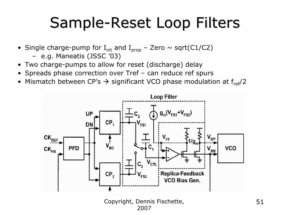
SampleSample--Reset Loop FiltersReset Loop Filters
• Single charge-pump for Iint and Iprop – Zero ~ sqrt(C1/C2)– e.g. Maneatis (JSSC ’03)
• Two charge-pumps to allow for reset (discharge) delay• Spreads phase correction over Tref – can reduce ref spurs• Mismatch between CP’s significant VCO phase modulation at fref/2
Copyright, Dennis Fischette, 2007
52
VoltageVoltage--Controlled Oscillator Controlled Oscillator (VCO)(VCO)
Copyright, Dennis Fischette, 2007
53
VoltageVoltage--Controlled OscillatorControlled Oscillator• VCO usually consists of two parts
– bias generator (e.g. Vctl to Ictl)– voltage or current controlled ring oscillator (RO)
• Typical VCO gain: Kvco ~ 1-5× * fmax. May vary w/PVT by > 2×
– need frequency range: >2× to allow for PVT
• RO delay stage may receive inputs from multiple prior stages (e.g. N-1 and N-2)
– allows N-stage VCO to oscillate at speeds otherwise attainable only by reducing # of stages
– easier to implement with differential signals
– extra care must be taken to ensure that RO will safely oscillate
Copyright, Dennis Fischette, 2007
54
VoltageVoltage--Controlled OscillatorControlled Oscillator
• Barkhausen criteria for sustained oscillation– loop gain must exceed 1, loop phase must equal 360°– more delay stages easier to initiate oscillation– gain(DC) > 2 for 3 stages, gain > sqrt(2) for 4 stages
• Quadrature clocks (0°, 90°, 180°, 270°) – requires 4 delay stages or– divide “differential” VCO outputs by 2, then delay one
set of divided outputs by ½ Tvco to generate quadratures. Allows any # of delay stages
Copyright, Dennis Fischette, 2007
55
PLL Suppression of VCO NoisePLL Suppression of VCO Noise• PLL acts like a high-pass filter in allowing VCO noise to reach
output
• Need noise-immune VCO to minimize jitter – Feedback loop cannot react quickly.
– Tradeoff between tuning range & noise sensitivity
• Power-supply noise is usually largest source of VCO noise
• VCO power-supply sensitivity should be at least 10-20× less than inverter
Copyright, Dennis Fischette, 2007
56
PLL Suppression of VCO NoisePLL Suppression of VCO Noise
• High power, fast edges, large swing low random jitter– Jrms ~sqrt(kT/2NC) / (fvco*Vswing)
• where N=#of stages, C=cap/stage
• Match rise/fall times, inter-stage delays to minimize phase noise (lowers ISF)
• RMS random jitter (kT) < 0.2% VCO period (typical)
Copyright, Dennis Fischette, 2007
57
VCO w/currentVCO w/current--starved starved inverters(CSI)inverters(CSI)
• Usually odd # of stages (usually 5+)• Feedback INV usually weaker by ~4ו Tune frequency by adjusting “VDD” of inverters – changes delay• “Vdd” for inverters is regulated output of VCO V2I
weakweakweak
Copyright, Dennis Fischette, 2007
58
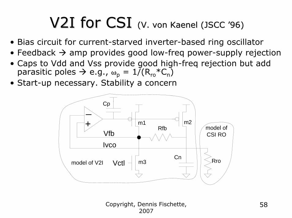
V2I for CSI V2I for CSI (V. von Kaenel (JSCC (V. von Kaenel (JSCC ’’96)96)
• Bias circuit for current-starved inverter-based ring oscillator• Feedback amp provides good low-freq power-supply rejection• Caps to Vdd and Vss provide good high-freq rejection but add
parasitic poles e.g., ωp = 1/(Rro*Cn)• Start-up necessary. Stability a concern
Ivco
Vctl
_+ m1 m2
Vfb
m3
Cp
Cn
Rfb
Rro
model ofCSI RO
model of V2I
Copyright, Dennis Fischette, 2007
59
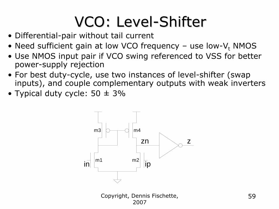
VCO: LevelVCO: Level--ShifterShifter• Differential-pair without tail current• Need sufficient gain at low VCO frequency – use low-Vt NMOS• Use NMOS input pair if VCO swing referenced to VSS for better
power-supply rejection• For best duty-cycle, use two instances of level-shifter (swap
inputs), and couple complementary outputs with weak inverters• Typical duty cycle: 50 ± 3%
in
z
m1 m2 ip
m3 m4
zn
Copyright, Dennis Fischette, 2007
60
Feedback DividerFeedback Divider
Copyright, Dennis Fischette, 2007
61
Feedback Divider (FBDIV)Feedback Divider (FBDIV)
• Typical Implementation: synchronous digital counter• Max FBDIV frequency should be greater than max VCO
frequency to avoid “run-away”– beware of Synthesized, Placed & Routed designs
• Counter output may glitch re-sample with VCO output to clean up glitch, reduce latency and phase noise
• Loop Phase Margin Degradation ~ ωc*Tfbdly
– usually insignificant (a few degrees)• Divider may be internal to PLL or after clock tree to cancel
clock tree skew• May provide additional output signals used to
deterministically synchronize tester controls to VCO clock and/or walk signals between various on-chip clock domains
Copyright, Dennis Fischette, 2007
62
Auxiliary CircuitsAuxiliary Circuits
Copyright, Dennis Fischette, 2007
63
Voltage RegulatorVoltage Regulator
• Provides stable, PVT-insensitive, clean power-supply for PLL– lower jitter, phase noise– more stable loop dynamics, VCO range, etc.– aim for > 30dB PSRR, definitely > 20dB
• Uses bandgap reference to set voltage and bias current levels
• Two voltage regulators sometime used– High VDD for charge-pump (analog) and lower VDD for VCO– “Quiet” for analog (CP, VCO bias) and “Dirty” for digital (PFD,
FBDIV)
Copyright, Dennis Fischette, 2007
64
Voltage RegulatorVoltage Regulator• Requires higher power-supply (e.g., 1.8V 1.2V)• Wastes current
– higher VDDA and bandgap/regulator over-head (0.5-3mA). – aim for current overhead < 20%. <5% is achievable in some
apps• Regulator area (inc. bandgap) is small compared to
decoupling cap area – Area (MOSFETs, Rpoly, diodes) ~ 70 x 70 µm2 (65nm)– Area (DECAPs) ~ 125µm x 125um for 100pF (65nm) – Typical cap ~ 30-200pF
• Vt-mismatch in bandgap amplifier input pair dominates overall regulator mismatch
– 3mV offset at amp ~20mV variation at output– Goal < 25mV 1-σ variation from device mismatch– Goal < ±5mV PVT variation (due mostly to diodes)
Copyright, Dennis Fischette, 2007
65
Digital PLLDigital PLL’’ss
Copyright, Dennis Fischette, 2007
66
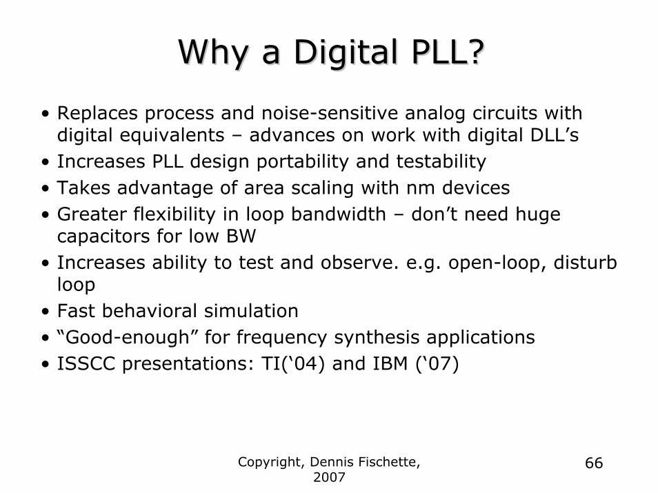
Why a Digital PLL?Why a Digital PLL?
• Replaces process and noise-sensitive analog circuits with digital equivalents – advances on work with digital DLL’s
• Increases PLL design portability and testability• Takes advantage of area scaling with nm devices• Greater flexibility in loop bandwidth – don’t need huge
capacitors for low BW• Increases ability to test and observe. e.g. open-loop, disturb
loop• Fast behavioral simulation• “Good-enough” for frequency synthesis applications• ISSCC presentations: TI(‘04) and IBM (‘07)
Copyright, Dennis Fischette, 2007
67
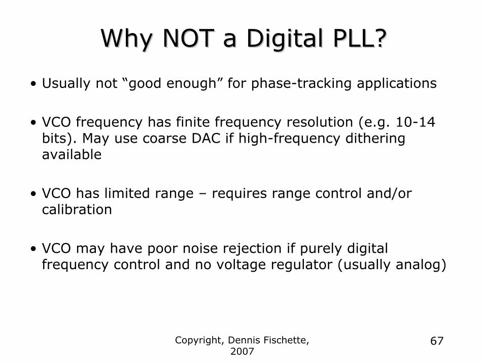
Why NOT a Digital PLL?Why NOT a Digital PLL?
• Usually not “good enough” for phase-tracking applications
• VCO frequency has finite frequency resolution (e.g. 10-14 bits). May use coarse DAC if high-frequency dithering available
• VCO has limited range – requires range control and/or calibration
• VCO may have poor noise rejection if purely digital frequency control and no voltage regulator (usually analog)
Copyright, Dennis Fischette, 2007
68
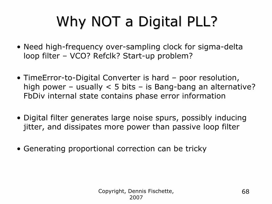
Why NOT a Digital PLL?Why NOT a Digital PLL?
• Need high-frequency over-sampling clock for sigma-delta loop filter – VCO? Refclk? Start-up problem?
• TimeError-to-Digital Converter is hard – poor resolution, high power – usually < 5 bits – is Bang-bang an alternative? FbDiv internal state contains phase error information
• Digital filter generates large noise spurs, possibly inducing jitter, and dissipates more power than passive loop filter
• Generating proportional correction can be tricky
Copyright, Dennis Fischette, 2007
69
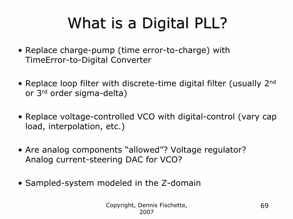
What is a Digital PLL?What is a Digital PLL?
• Replace charge-pump (time error-to-charge) with TimeError-to-Digital Converter
• Replace loop filter with discrete-time digital filter (usually 2nd
or 3rd order sigma-delta)
• Replace voltage-controlled VCO with digital-control (vary cap load, interpolation, etc.)
• Are analog components “allowed”? Voltage regulator? Analog current-steering DAC for VCO?
• Sampled-system modeled in the Z-domain
Copyright, Dennis Fischette, 2007
70
Circuit VerificationCircuit Verification
Copyright, Dennis Fischette, 2007
71
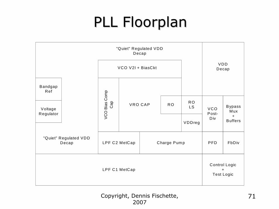
PLL FloorplanPLL Floorplan
RO ROLSVRO CAP
VCO V2I + B iasCkt
VC
O B
ias
Com
pC
ap
PFDCharge Pum p
VCOPost-D iv
FbDiv
BypassMux
+Buffers
Control Logic+
Test Logic
BandgapRef
VoltageRegulator
LPF C2 MetCap
LPF C1 MetCap
VDDDecap
"Quiet" Regulated VDDDecap
"Quiet" Regulated VDDDecap
VDDreg

Copyright, Dennis Fischette, 2007
72
Noise IsolationNoise Isolation
• Check extracted netlist for coupling of switching signals onto sensitive analog signals (e.g. REFCLK Vctl)
• Check that LPF metal caps are present and well-connected to correct power supplies
• Check that VSS of LPF metal caps and VSS of VCO bias circuits are well-connected and at same potential
• Check that correct shields for sensitive signals are in place and well-tied to correct power supplies
Copyright, Dennis Fischette, 2007
73
Noise IsolationNoise Isolation
• Account for parasitic capacitance to substrate in “NWELL”decaps, diodes, and well/diffusion resistors
• Add guard rings as applicable
• Buffer control signals and programmable inputs locally before use
– avoids problem where GND of control signal doesn’t match local GND where signal is used
– filters coupling/glitches on long routes
Copyright, Dennis Fischette, 2007
74
Signal EM / ESDSignal EM / ESD
• Inspect wires that conduct DC current and wires that drive large switching output loads for EM violations (e.g. charge-pump bias, output clocks)
• Check that signal ESD and/or power supply clamps are well-connected to power supplies (< 1-2 Ω)
– extract power grids and ESD– simulate for voltage peaks and diodes wired-backward
Copyright, Dennis Fischette, 2007
75
PowerPower--Grid IRGrid IR
• Aim for avg IR drops < 5mV over entire PLL, less within and between related analog blocks
• Decoupling capacitors surround large, switching buffers to reduce IR drops and are well-connected to grid
• Check for isolated power domain islands
• Plan power domains and level-shifter placement up-front
Copyright, Dennis Fischette, 2007
76
Switching SignalsSwitching Signals
• Match differential signals – total capacitance and coupling (e.g. up, up_x, dn, dn_x, clk, clk_x)
– try to match total capacitance < 1-2%
• Maintain fanout (incl. Wires) < ~6 on high-speed paths, < ~10 on DC paths (e.g. encode/decoders)
– reduces crow-bar current and noise glitches
• Setup/Hold checks in PFD, Feedback Divider, and Post-VCO divider. Needs lots of margin for FBDIV to account for overshoot, aging, etc.
– strive for FBDIV faster than VCO(max)
Copyright, Dennis Fischette, 2007
77
PLL Instantiation PLL Instantiation –– Visual ChecksVisual Checks
• Mismatch on differential signals
• Coupling into refclk, output clocks
• Possible glitches on control inputs
• Signal routes over sensitive areas of PLL (VCO, loop filter, charge-pump)
• Large buffers on edge of PLL that may inject noise in substrate (keep-out requirement?)
Copyright, Dennis Fischette, 2007
78
PLL Instantiation PLL Instantiation –– Visual ChecksVisual Checks
• Output wires wide enough to handle current load (EM)
• Rise/fall times on inputs/outputs – add max_cap limit into timing file to flag heavy loads
• VDDA/test signal routes to bumps and/or ESD
• VDD/ VSS power supply connections
Copyright, Dennis Fischette, 2007
79
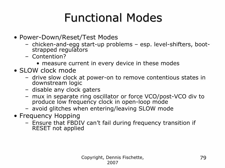
Functional ModesFunctional Modes
• Power-Down/Reset/Test Modes– chicken-and-egg start-up problems – esp. level-shifters, boot-
strapped regulators– Contention?
• measure current in every device in these modes• SLOW clock mode
– drive slow clock at power-on to remove contentious states in downstream logic
– disable any clock gaters– mux in separate ring oscillator or force VCO/post-VCO div to
produce low frequency clock in open-loop mode– avoid glitches when entering/leaving SLOW mode
• Frequency Hopping– Ensure that FBDIV can’t fail during frequency transition if
RESET not applied
Copyright, Dennis Fischette, 2007
80
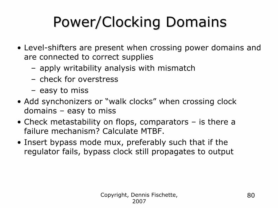
Power/Clocking DomainsPower/Clocking Domains
• Level-shifters are present when crossing power domains and are connected to correct supplies
– apply writability analysis with mismatch– check for overstress– easy to miss
• Add synchonizers or “walk clocks” when crossing clock domains – easy to miss
• Check metastability on flops, comparators – is there a failure mechanism? Calculate MTBF.
• Insert bypass mode mux, preferably such that if the regulator fails, bypass clock still propagates to output
Copyright, Dennis Fischette, 2007
81
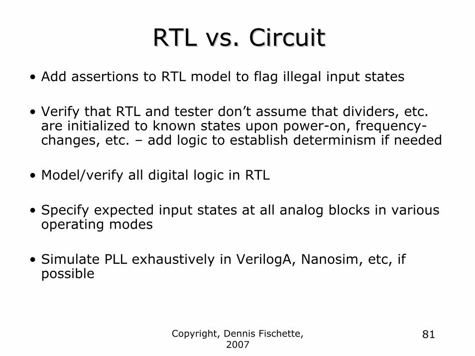
RTL vs. CircuitRTL vs. Circuit• Add assertions to RTL model to flag illegal input states
• Verify that RTL and tester don’t assume that dividers, etc. are initialized to known states upon power-on, frequency-changes, etc. – add logic to establish determinism if needed
• Model/verify all digital logic in RTL
• Specify expected input states at all analog blocks in various operating modes
• Simulate PLL exhaustively in VerilogA, Nanosim, etc, if possible
Copyright, Dennis Fischette, 2007
82
RTL vs. CircuitRTL vs. Circuit
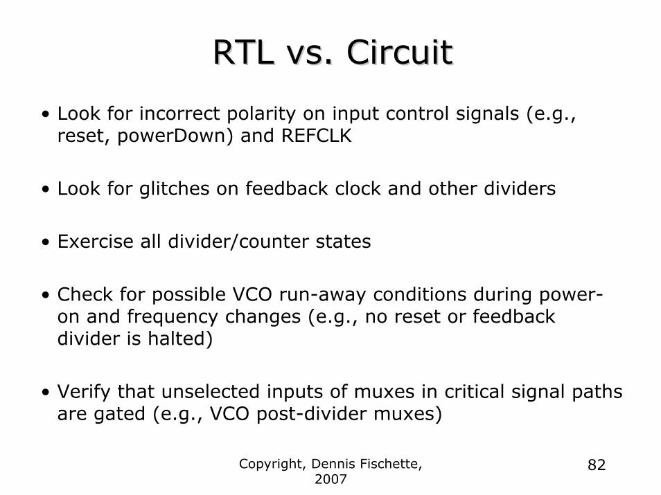
• Look for incorrect polarity on input control signals (e.g., reset, powerDown) and REFCLK
• Look for glitches on feedback clock and other dividers
• Exercise all divider/counter states
• Check for possible VCO run-away conditions during power-on and frequency changes (e.g., no reset or feedback divider is halted)
• Verify that unselected inputs of muxes in critical signal paths are gated (e.g., VCO post-divider muxes)
Copyright, Dennis Fischette, 2007
83
Behavioral SimulationsBehavioral Simulations• Behavioral simulation –before detailed circuit design define
requirements for each block – e.g. PLLUS, Simulink
• Develop/verify jitter budget – e.g. PCI-Express
• Estimate VCO frequency overshoot
• Loop bandwidth vs. reference noise suppression
• Simulate effects of loop filter leakage, charge-pump mismatch, feedback delays, OSR, spread-spectrum tracking, Vctl-sensitive loop parameters, PFD dead-zone, parasitic poles
Copyright, Dennis Fischette, 2007
84
Circuit SimulationsCircuit Simulations
• Start-up circuit safety margin - bandgap, VCO, regulators• Stability of all internal feedback loops
– AC and transient impulse response – e.g., bandgap, regulator, charge-pump bias, VCO bias– Phase margin, gain margin, # of rings
• VCO - RO stage delays rise vs. fall, stage-to-stage – lower ISF
• Level-shifters’ possible corruption of duty-cycle• Switching-induced noise spikes on regulated power supplies• Current dissipation in power
Copyright, Dennis Fischette, 2007
85
Circuit SimulationsCircuit Simulations
• PSRR of voltage regulators, ability of regulators to meet fast-changing current load
• Step reference phase, observe PLL re-lock– overshoot, relock time
• Simulate entire sequence from power-on to lock– sanity check
Copyright, Dennis Fischette, 2007
86
Devices/CircuitsDevices/Circuits
• Estimate effects of Vt mismatch BEFORE starting layout (monte carlo, dVt ~ 1/sqrt(W*L) )
– most sensitive: bandgap, charge-pump, other low I ckts
• Estimate loop parameter variations, static error, reference spurs due to PVT and mismatch before starting layout
– Kv, Icp, R, C1 (also vs. Vctl) – esp. dual- charge-pump designs– circuit techniques to minimize effects: self-bias,
Icp*Rlpf=const– self-bias not as effective if not all devices the same Leff
• Diode current density (bandgap) – ideality factor may be sensitive to current density – stay away from cliff
Copyright, Dennis Fischette, 2007
87
Device ReliabilityDevice Reliability
• Gate Overstress– especially likely during power-down, reset, test– hspice .biaschk is useful
• Gate Leakage– LPF especially, Ileak(LPF) < a few nA– Switches used for test modes– Gate loads of high-impedance nodes (e.g. bandgap)– Large op-amp inputs
Copyright, Dennis Fischette, 2007
88
Device ReliabilityDevice Reliability
• Verify that circuits with PMOS devices are not NBTI-sensitive
– Vgs of matched devices should be the same at all times, even when not selected (e.g. current-steering DAC) –don’t place switches closest supply rails
– switching circuits such as VCO and FBDIV should have enough frequency headroom to allow for aging. High Vgsis bad! 10-20% margin?
– effect worse at 45nm and 65nm and may not be well-modeled
Copyright, Dennis Fischette, 2007
89
Lithography/DevicesLithography/Devices
• Add dummy poly to reduce ACLV (across chip linewidth variation), esp. in Lmin devices
• Maintain gate poly on fixed pitch in same orientation to reduce ACLV (esp. in Lmin devices)
• Try to maintain constant poly density – e.g. no large caps next to sensitive Lmin devices)
• Add dummy devices if stress/strain is applied and matching is required (e.g., charge-pump)
Copyright, Dennis Fischette, 2007
90
Tips for Design for TestTips for Design for Test
• Measuring Jitter and Phase Error
• Measuring Loop Dynamics
• Analog Measurements
• Probing
Copyright, Dennis Fischette, 2007
91
Getting Clocks from PLL to BoardGetting Clocks from PLL to Board
• Differential I/O outputs highly desirable to reject common-mode noise – use fastest I/O available
• Divide VCO to reduce board attenuation only if necessary make divider programmable
• Measuring duty-cycle– Divide-by-odd-integer– Mux to select either true or inverted VCO clock. Duty-
cycle error = (Duty+ - Duty-) / 2
Copyright, Dennis Fischette, 2007
92
Getting Clocks from PLL to BoardGetting Clocks from PLL to Board
• Ability to disable neighboring I/O when measuring jitter
• Observe REF, VCO, and FBCLK. Gate unused inputs to the clock source mux
• Phase error measurement: trigger scope on REFCLK on board. Capture internal REFCLK and FBCLK in infinite persistence. Measure difference between internal REFCLK and FBCLK on same pin.
Copyright, Dennis Fischette, 2007
93
Measuring Loop DynamicsMeasuring Loop Dynamics
• Modulate reference phase at various modulation frequencies and measure VCO phase using TIE
– used to construct closed-loop transfer function
• On-chip state-machines– range from simple to sophisticated– disturb locked PLL in some way and observe re-lock
behavior
Copyright, Dennis Fischette, 2007
94
Analog MeasurementsAnalog Measurements
• Need ability to measure key internal analog signals without injecting noise
– Loop filter control voltage– Ring Oscillator regulated supply– Bandgap reference– Regulated power supplies– Charge-pump bias voltages and currents
• Metrics– Measurement BW ~ PLL Bandwidth or less– Accuracy ~ 5mV?– Programmable via JTAG
Copyright, Dennis Fischette, 2007
95
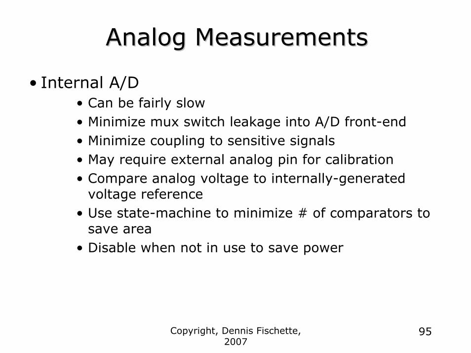
Analog MeasurementsAnalog Measurements
• Internal A/D• Can be fairly slow• Minimize mux switch leakage into A/D front-end• Minimize coupling to sensitive signals• May require external analog pin for calibration• Compare analog voltage to internally-generated
voltage reference• Use state-machine to minimize # of comparators to
save area• Disable when not in use to save power
Copyright, Dennis Fischette, 2007
96
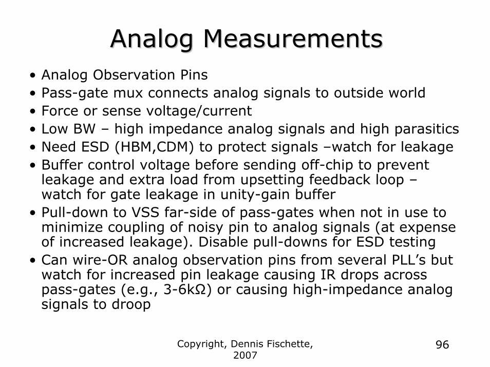
Analog MeasurementsAnalog Measurements• Analog Observation Pins• Pass-gate mux connects analog signals to outside world• Force or sense voltage/current• Low BW – high impedance analog signals and high parasitics• Need ESD (HBM,CDM) to protect signals –watch for leakage• Buffer control voltage before sending off-chip to prevent
leakage and extra load from upsetting feedback loop –watch for gate leakage in unity-gain buffer
• Pull-down to VSS far-side of pass-gates when not in use to minimize coupling of noisy pin to analog signals (at expense of increased leakage). Disable pull-downs for ESD testing
• Can wire-OR analog observation pins from several PLL’s but watch for increased pin leakage causing IR drops across pass-gates (e.g., 3-6kΩ) or causing high-impedance analog signals to droop
Copyright, Dennis Fischette, 2007
97
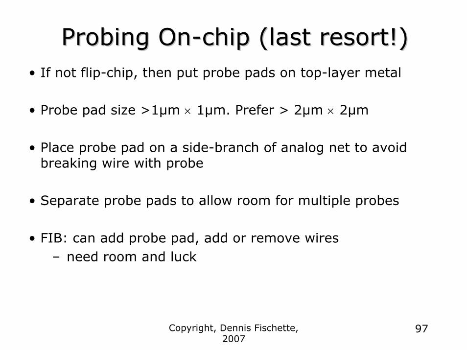
Probing OnProbing On--chip (last resort!)chip (last resort!)• If not flip-chip, then put probe pads on top-layer metal
• Probe pad size >1µm × 1µm. Prefer > 2µm × 2µm
• Place probe pad on a side-branch of analog net to avoid breaking wire with probe
• Separate probe pads to allow room for multiple probes
• FIB: can add probe pad, add or remove wires– need room and luck
Copyright, Dennis Fischette, 2007
98
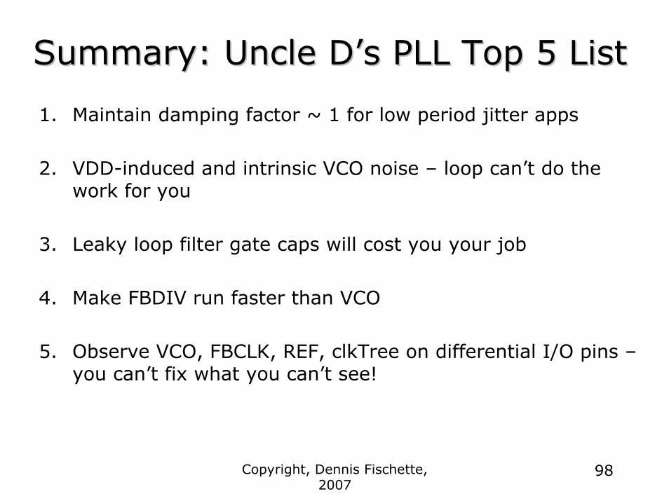
Summary: Uncle DSummary: Uncle D’’s PLL Top 5 Lists PLL Top 5 List
1. Maintain damping factor ~ 1 for low period jitter apps
2. VDD-induced and intrinsic VCO noise – loop can’t do the work for you
3. Leaky loop filter gate caps will cost you your job
4. Make FBDIV run faster than VCO
5. Observe VCO, FBCLK, REF, clkTree on differential I/O pins –you can’t fix what you can’t see!
Copyright, Dennis Fischette, 2007
99
Special thanks to Alvin Loke for Special thanks to Alvin Loke for allowing to me allowing to me ““borrowborrow”” some of his some of his
diagrams and ideas for this talkdiagrams and ideas for this talk……which which ones? The good onesones? The good ones
Copyright, Dennis Fischette, 2007
100
ReferencesReferences
Copyright, Dennis Fischette, 2007
101
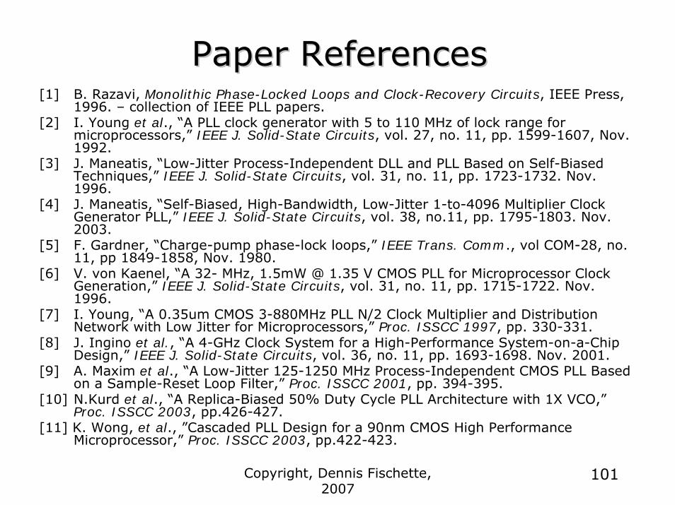
Paper ReferencesPaper References[1] B. Razavi, Monolithic Phase-Locked Loops and Clock-Recovery Circuits, IEEE Press,
1996. – collection of IEEE PLL papers.[2] I. Young et al., “A PLL clock generator with 5 to 110 MHz of lock range for
microprocessors,” IEEE J. Solid-State Circuits, vol. 27, no. 11, pp. 1599-1607, Nov. 1992.
[3] J. Maneatis, “Low-Jitter Process-Independent DLL and PLL Based on Self-Biased Techniques,” IEEE J. Solid-State Circuits, vol. 31, no. 11, pp. 1723-1732. Nov. 1996.
[4] J. Maneatis, “Self-Biased, High-Bandwidth, Low-Jitter 1-to-4096 Multiplier Clock Generator PLL,” IEEE J. Solid-State Circuits, vol. 38, no.11, pp. 1795-1803. Nov. 2003.
[5] F. Gardner, “Charge-pump phase-lock loops,” IEEE Trans. Comm., vol COM-28, no. 11, pp 1849-1858, Nov. 1980.
[6] V. von Kaenel, “A 32- MHz, 1.5mW @ 1.35 V CMOS PLL for Microprocessor Clock Generation,” IEEE J. Solid-State Circuits, vol. 31, no. 11, pp. 1715-1722. Nov. 1996.
[7] I. Young, “A 0.35um CMOS 3-880MHz PLL N/2 Clock Multiplier and Distribution Network with Low Jitter for Microprocessors,” Proc. ISSCC 1997, pp. 330-331.
[8] J. Ingino et al., “A 4-GHz Clock System for a High-Performance System-on-a-Chip Design,” IEEE J. Solid-State Circuits, vol. 36, no. 11, pp. 1693-1698. Nov. 2001.
[9] A. Maxim et al., “A Low-Jitter 125-1250 MHz Process-Independent CMOS PLL Based on a Sample-Reset Loop Filter,” Proc. ISSCC 2001, pp. 394-395.
[10] N.Kurd et al., “A Replica-Biased 50% Duty Cycle PLL Architecture with 1X VCO,”Proc. ISSCC 2003, pp.426-427.
[11] K. Wong, et al., ”Cascaded PLL Design for a 90nm CMOS High Performance Microprocessor,” Proc. ISSCC 2003, pp.422-423.
Copyright, Dennis Fischette, 2007
102
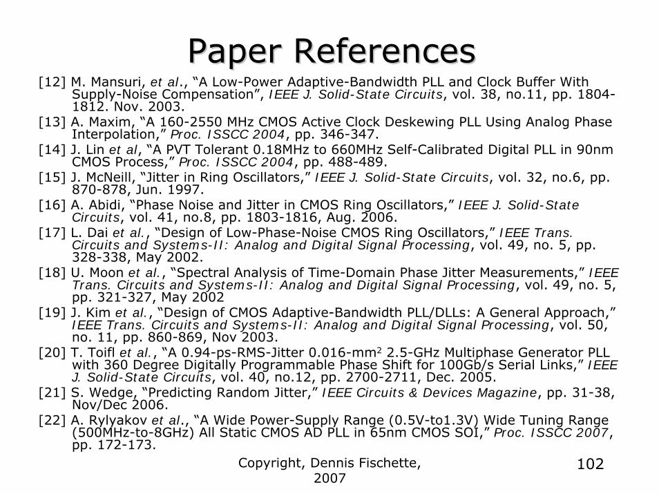
Paper ReferencesPaper References[12] M. Mansuri, et al., “A Low-Power Adaptive-Bandwidth PLL and Clock Buffer With
Supply-Noise Compensation”, IEEE J. Solid-State Circuits, vol. 38, no.11, pp. 1804-1812. Nov. 2003.
[13] A. Maxim, “A 160-2550 MHz CMOS Active Clock Deskewing PLL Using Analog Phase Interpolation,” Proc. ISSCC 2004, pp. 346-347.
[14] J. Lin et al, “A PVT Tolerant 0.18MHz to 660MHz Self-Calibrated Digital PLL in 90nm CMOS Process,” Proc. ISSCC 2004, pp. 488-489.
[15] J. McNeill, “Jitter in Ring Oscillators,” IEEE J. Solid-State Circuits, vol. 32, no.6, pp. 870-878, Jun. 1997.
[16] A. Abidi, “Phase Noise and Jitter in CMOS Ring Oscillators,” IEEE J. Solid-State Circuits, vol. 41, no.8, pp. 1803-1816, Aug. 2006.
[17] L. Dai et al., “Design of Low-Phase-Noise CMOS Ring Oscillators,” IEEE Trans. Circuits and Systems-II: Analog and Digital Signal Processing, vol. 49, no. 5, pp. 328-338, May 2002.
[18] U. Moon et al., “Spectral Analysis of Time-Domain Phase Jitter Measurements,” IEEE Trans. Circuits and Systems-II: Analog and Digital Signal Processing, vol. 49, no. 5, pp. 321-327, May 2002
[19] J. Kim et al., “Design of CMOS Adaptive-Bandwidth PLL/DLLs: A General Approach,”IEEE Trans. Circuits and Systems-II: Analog and Digital Signal Processing, vol. 50, no. 11, pp. 860-869, Nov 2003.
[20] T. Toifl et al., “A 0.94-ps-RMS-Jitter 0.016-mm2 2.5-GHz Multiphase Generator PLL with 360 Degree Digitally Programmable Phase Shift for 100Gb/s Serial Links,” IEEE J. Solid-State Circuits, vol. 40, no.12, pp. 2700-2711, Dec. 2005.
[21] S. Wedge, “Predicting Random Jitter,” IEEE Circuits & Devices Magazine, pp. 31-38, Nov/Dec 2006.
[22] A. Rylyakov et al., “A Wide Power-Supply Range (0.5V-to1.3V) Wide Tuning Range (500MHz-to-8GHz) All Static CMOS AD PLL in 65nm CMOS SOI,” Proc. ISSCC 2007, pp. 172-173.
Copyright, Dennis Fischette, 2007
103
Paper ReferencesPaper References
[24] R. Staszewski et al, “All-Digital PLL and Transmitter for Mobile Phones,” IEEE J. Solid-State Circuits, vol. 40, no.12, pp. 2469-2482. Dec. 2005.
[25] R. Staszewski et al, “All-Digital PLL with Ultra Fast Settling,” IEEE Trans. On Circuits and Systems II: Express Briefs, vol. 54, no.2, pp. 181-185. Feb. 2007.
[26] V. Kratyuk et al, “A Design Procedure for All-Digital Phase-Locked Loops Based on a Charge-Pump Phase-Locked-Loop Analogy,” IEEE Trans. On Circuits and Systems II: Express Briefs, vol. 54, no.3, pp. 247-251. Mar. 2007.
[27] J. Hein et al, “z-Domain Model for Discrete-Time PLL’s,” IEEE Trans. On Circuits and Systems, vol. 35, no.11, pp. 1393-1400. Nov. 1988.
Copyright, Dennis Fischette, 2007
104
Monograph ReferencesMonograph References
[1] B. Razavi, Design of Analog CMOS Integrated Circuits, McGraw-Hill, 2001.[2] R. Best, Phase-Locked Loops,McGraw-Hill, 1993.[3] R. Dorf, Modern Control Theory, 4th Edition, Addison-Wesley, 1986.[4] P.Gray and R. Meyer, Analysis and Design of Analog Integrated Circuits, 3rd Edition, J.
Wiley & Sons, 1993.[5] K. Bernstein and N. Rohner, SOI Circuit Design Concepts, Kluwer Academic Publishers,
2000.[6] A. Hajimiri and T. Lee, The Design of Low Noise Oscillators, Kluwer Academic
Publishers, 1999.[7] T. Lee, The Design of CMOS Radio-Frequency Integrated Circuits, Cambridge
University Press, 1998. [8] F. Gardner, Phaselock Techniques, 2nd Edition, New York, Wiley & Sons, 1979.
Copyright, Dennis Fischette, 2007
105
PLL FailuresPLL Failures
Copyright, Dennis Fischette, 2007
106
PLL FailuresPLL Failures
• Observation is that VCO frequency is pinned at max value. Can’t observe Vctl or feedback clock. VCO fails to oscillate at low frequency because of insufficient gain in 3-stage VCO. When VCO finally starts, FBDIV can’t keep up, causing “run-away” Solution: increase gain of delay stage and FBDIV speed.
• VCO “run-away” when re-locking to higher frequency due to VCO overshoot and slow FBDIV.
• VCO loses lock occasionally at low frequencies. Due to insufficient VCO level-shifter gain. Dropped VCO edges. Required real-time scope for debug
• High jitter at low VCO frequencies due to Vctl approaching Vt of V2I current source. Solution: operate VCO at 2X.
Copyright, Dennis Fischette, 2007
107
PLL FailuresPLL Failures
• Occasional high deterministic jitter caused by coupling into PLL’s VDDA bondwire.
• Extremely high period jitter – caused by incorrect wiring of 8-bit charge-pump setting. Bandwidth much too high. Verilog model did not check for legal input settings.
• PLL won’t start-up at low temp due to weak start-up circuit in voltage regulator and lack of simulation at corners with slow VDDA ramp-rate.
• PLL period modulated strongly by 400MHz signal, resulting from oscillating internal feedback loop in VCO bias ckts. Ultimate cause, fab misprocessing of compensation cap and insufficient margin in ckt.
Copyright, Dennis Fischette, 2007
108
PLL FailuresPLL Failures
• Metastability condition corrupted digital loop filter due to slow devices, low Vdd, and insufficient design margin.
• Digital VCO out-of-range due to resistor mis-processing. Solution: fusable chicken-bits to adjust frequency range.
• Race condition in digital loop filter caused by missing synchonizers in clock domain crossing.
Copyright, Dennis Fischette, 2007
109
PLL FailuresPLL Failures
• CDM ESD failures of analog measurement pins – no visual inspection and no extraction/simulation of connection to VSS.
• Duty-cycle corruption (> 57%) – caused by unbalanced fanouts in delay stages after VCO – exacerbated by single-ended clocking.
• Contention in analog observation signals due to ESD diodes wired backward and control logic bugs.
• Inconsistent duty cycle. Failure to initialize state in post-VCO divider exposed VCO duty-cycle error.