Low Temperature Homoepitaxy Of (010) -Ga O By Metalorganic ...
5
1 Low Temperature Homoepitaxy Of (010) β -Ga 2 O 3 By Metalorganic Vapor Phase Epitaxy : Expanding The Growth Window Arkka Bhattacharyya,Praneeth Ranga, Saurav Roy, Jonathan Ogle, Luisa Whittaker-Brooks, and Sriram Krishnamoorthy Abstract—In this work, we report on the growth of high- mobility β-Ga2O3 homoepitaxial thin films grown at a tem- perature much lower than the conventional growth temperature window for metalorganic vapor phase epitaxy. Low-temperature β-Ga2O3 thin films grown at 600 ◦ C on Fe-doped (010) bulk substrates exhibits remarkable crystalline quality which is evi- dent from the measured room temperature Hall mobility of 186 cm 2 /Vs for the unintentionally doped films. N-type doping is achieved by using Si as a dopant and a controllable doping in the range of 2×10 16 -2×10 19 cm -3 is studied. Si incorporation and activation is studied by comparing silicon concentration from secondary ion mass spectroscopy (SIMS) and electron concentration from temperature-dependent Hall measurements. The films exhibit high purity (low C and H concentrations) with very low concentration of compensating acceptors (2×10 15 cm -3 ) even at this growth temperature. Additionally, abrupt doping profile with forward decay of ∼ 5nm/dec (10 times improvement compared to what is observed for thin films grown at 810 ◦ C) is demonstrated by growing at a lower temperature. Index Terms—gallium oxide, MOVPE, high-mobility, low tem- perature, abrupt doping, epitaxy, Hall Effect, secondary ion mass spectroscopy I. I NTRODUCTION B ETA -Ga 2 O 3 is the emerging material of choice for power device applications owing to its material properties that translates to predicted Baliga figure of merit (BFOM) several times larger than SiC and GaN [1]. To reach this intrinsic potential, a material with low background doping and high mobility is necessary. Carrier transport in β-Ga 2 O 3 suffers from severe polar optical phonon scattering that limits its theoretical room temperature mobility to 200 cm 2 /Vs [2]. Metalorganic vapor phase epitaxy (MOVPE) has emerged as the leading growth technique that allows for the growth of epi- taxial films with mobility values closer to this theoretical limit [3]. So far, the homoepitaxy of β-Ga 2 O 3 using MOVPE has been demonstrated with different reactor geometries, different precursors, dopants and on different substrate orientations. All the growth and doping studies done on these homoepitaxial β- Ga 2 O 3 thin films are typically performed at high temperatures (>800 ◦ C) [4]–[11]. The lower temperature regime <800 ◦ C still remains unexplored and could help in furthering the understanding of the growth window for β-Ga 2 O 3 epitaxy. Arkka Bhattacharyya, Praneeth Ranga, Saurav Roy, and Sriram Krish- namoorthy are with the Department of Electrical and Computer Engineering, The University of Utah, Salt Lake City, UT, 84112, United States of America (e-mail: [email protected], [email protected] ). Jonathan Ogle and Luisa Whittaker-Brooks are with the Department of Chemistry, University of Utah, Salt Lake City, Utah 84112, USA. The low temperature epitaxial growth (LT) of β-Ga 2 O 3 is interesting to study especially for the development of power and high-frequency (RF) devices. Dopant incorporation, des- orption and segregation in semiconductor growth are strongly correlated to the growth temperature and could be better controlled if films are grown at lower temperatures. The effect of these phenomena could be very important in the development of 2D channel RF devices such as delta-doped and modulation-doped FETs where extremely sharp doping profiles become critical. Another key application of MOVPE LT epitaxy could be the ohmic contact regrowth process to buried channel structures that could expand the capability of the MOVPE technique in terms of device processing [12], [13]. Regrowth process if done at high temperatures could lead to dopant diffusion, creation and migration of defects in the active region that could result in channels with reduced mobility. Here, we explore the low temperature regime of the MOVPE growth window by tuning the growth temperature down to 600 ◦ C. We show that β-Ga 2 O 3 thin films with with electronic properties similar to thin films grown at higher temperatures are achievable. This allows us to expand the growth window of MOVPE by almost more than 200 ◦ C. Furthermore, we demonstrate sharp silicon doping profile enabled by low temperature epitaxy. β-Ga 2 O 3 thin films were grown on Fe-doped (010) semi- insulating bulk substrates (Novel Crystal Technology, Japan) in an MOVPE reactor (Agnitron Agilis) using triethylgallium (TEGa), O 2 and diluted silane as precursors and argon as the carrier gas. Growths were carried out at substrate temperatures (T g ) of 550 - 810 ◦ C. Prior to loading the substrates into the growth chamber, the substrates were cleaned with acetone, methanol and DI water followed by a 30 min dip in a diluted HF solution [3]. Films with thicknesses 400-1000 nm were grown. Uniformity of the doping profile were characterized by capacitance-voltage (CV) measurements on lateral Schottky diode structures with Ni/Au Schottky pads and Ti/Au Ohmic contacts. The films were grown at growth temperatures of T g = 550 ◦ C, 600 ◦ C, 700 ◦ C and 810 ◦ C. The precursor flow values were set to 65 sccm, 800 sccm, 1100 sccm for TEGa, O 2 , Ar respectively and the chamber pressure was maintained at 60 Torr. By keeping all other growth conditions identical, T g was the only growth parameter varied . Figure 1 shows the atomic force microscopy (AFM) scans of the surface morphology of representative films grown at (a) 700 ◦ C, (b) 600 ◦ C and (c) 550 ◦ C. The films grown at T g = 600 ◦ C and 700 ◦ C show arXiv:2008.00303v1 [physics.app-ph] 1 Aug 2020
Transcript of Low Temperature Homoepitaxy Of (010) -Ga O By Metalorganic ...
1
Low Temperature Homoepitaxy Of (010) β-Ga2O3
By Metalorganic Vapor Phase Epitaxy : ExpandingThe Growth Window
Arkka Bhattacharyya,Praneeth Ranga, Saurav Roy, Jonathan Ogle, Luisa Whittaker-Brooks, andSriram Krishnamoorthy
Abstract—In this work, we report on the growth of high-mobility β-Ga2O3 homoepitaxial thin films grown at a tem-perature much lower than the conventional growth temperaturewindow for metalorganic vapor phase epitaxy. Low-temperatureβ-Ga2O3 thin films grown at 600◦C on Fe-doped (010) bulksubstrates exhibits remarkable crystalline quality which is evi-dent from the measured room temperature Hall mobility of 186cm2/Vs for the unintentionally doped films. N-type doping isachieved by using Si as a dopant and a controllable doping inthe range of 2×10¹⁶ - 2×1019 cm−3 is studied. Si incorporationand activation is studied by comparing silicon concentrationfrom secondary ion mass spectroscopy (SIMS) and electronconcentration from temperature-dependent Hall measurements.The films exhibit high purity (low C and H concentrations) withvery low concentration of compensating acceptors (2×1015 cm−3)even at this growth temperature. Additionally, abrupt dopingprofile with forward decay of ∼ 5nm/dec (10 times improvementcompared to what is observed for thin films grown at 810◦C) isdemonstrated by growing at a lower temperature.
Index Terms—gallium oxide, MOVPE, high-mobility, low tem-perature, abrupt doping, epitaxy, Hall Effect, secondary ion massspectroscopy
I. INTRODUCTION
BETA -Ga2O3 is the emerging material of choice for powerdevice applications owing to its material properties that
translates to predicted Baliga figure of merit (BFOM) severaltimes larger than SiC and GaN [1]. To reach this intrinsicpotential, a material with low background doping and highmobility is necessary. Carrier transport in β-Ga2O3 suffersfrom severe polar optical phonon scattering that limits itstheoretical room temperature mobility to 200 cm2/Vs [2].Metalorganic vapor phase epitaxy (MOVPE) has emerged asthe leading growth technique that allows for the growth of epi-taxial films with mobility values closer to this theoretical limit[3]. So far, the homoepitaxy of β-Ga2O3 using MOVPE hasbeen demonstrated with different reactor geometries, differentprecursors, dopants and on different substrate orientations. Allthe growth and doping studies done on these homoepitaxial β-Ga2O3 thin films are typically performed at high temperatures(>800◦C) [4]–[11]. The lower temperature regime <800◦Cstill remains unexplored and could help in furthering theunderstanding of the growth window for β-Ga2O3 epitaxy.
Arkka Bhattacharyya, Praneeth Ranga, Saurav Roy, and Sriram Krish-namoorthy are with the Department of Electrical and Computer Engineering,The University of Utah, Salt Lake City, UT, 84112, United States of America(e-mail: [email protected], [email protected] ).
Jonathan Ogle and Luisa Whittaker-Brooks are with the Department ofChemistry, University of Utah, Salt Lake City, Utah 84112, USA.
The low temperature epitaxial growth (LT) of β-Ga2O3 isinteresting to study especially for the development of powerand high-frequency (RF) devices. Dopant incorporation, des-orption and segregation in semiconductor growth are stronglycorrelated to the growth temperature and could be bettercontrolled if films are grown at lower temperatures. Theeffect of these phenomena could be very important in thedevelopment of 2D channel RF devices such as delta-dopedand modulation-doped FETs where extremely sharp dopingprofiles become critical. Another key application of MOVPELT epitaxy could be the ohmic contact regrowth process toburied channel structures that could expand the capability ofthe MOVPE technique in terms of device processing [12],[13]. Regrowth process if done at high temperatures couldlead to dopant diffusion, creation and migration of defects inthe active region that could result in channels with reducedmobility. Here, we explore the low temperature regime of theMOVPE growth window by tuning the growth temperaturedown to 600◦C. We show that β-Ga2O3 thin films with withelectronic properties similar to thin films grown at highertemperatures are achievable. This allows us to expand thegrowth window of MOVPE by almost more than 200◦C.Furthermore, we demonstrate sharp silicon doping profileenabled by low temperature epitaxy.β-Ga2O3 thin films were grown on Fe-doped (010) semi-
insulating bulk substrates (Novel Crystal Technology, Japan)in an MOVPE reactor (Agnitron Agilis) using triethylgallium(TEGa), O2 and diluted silane as precursors and argon as thecarrier gas. Growths were carried out at substrate temperatures(Tg) of 550 - 810◦C. Prior to loading the substrates into thegrowth chamber, the substrates were cleaned with acetone,methanol and DI water followed by a 30 min dip in a dilutedHF solution [3]. Films with thicknesses 400-1000 nm weregrown. Uniformity of the doping profile were characterizedby capacitance-voltage (CV) measurements on lateral Schottkydiode structures with Ni/Au Schottky pads and Ti/Au Ohmiccontacts.
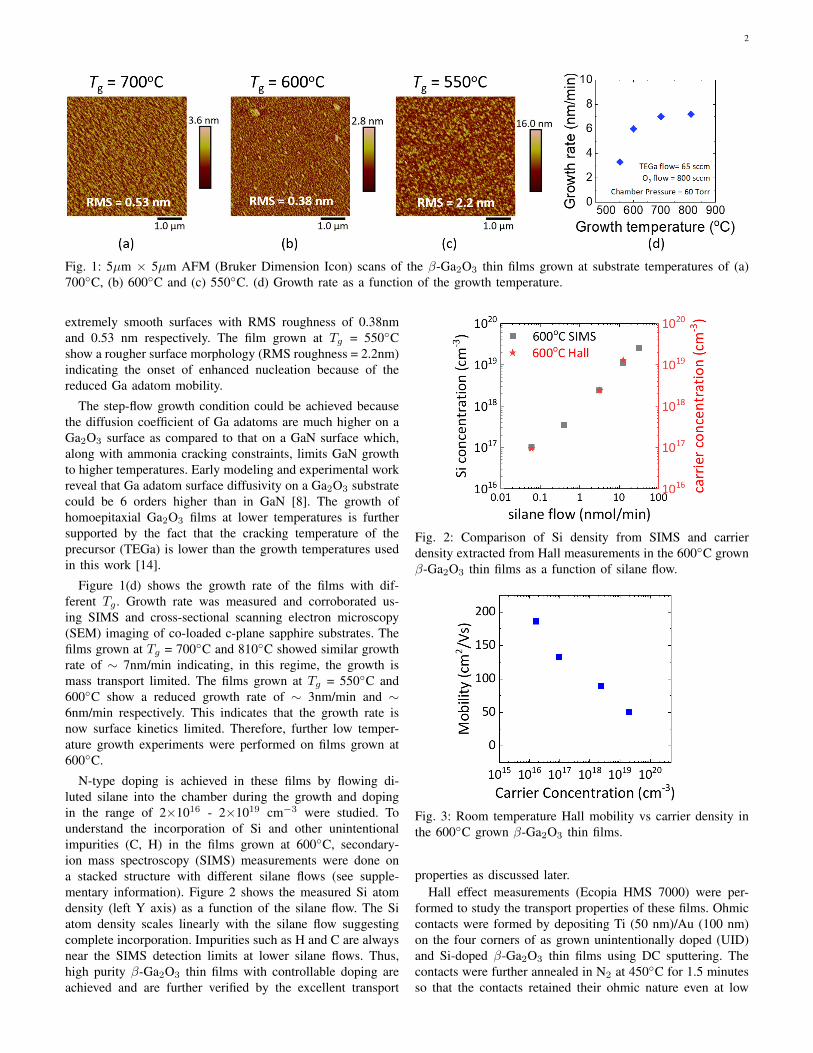
The films were grown at growth temperatures of Tg =550◦C, 600◦C, 700◦C and 810◦C. The precursor flow valueswere set to 65 sccm, 800 sccm, 1100 sccm for TEGa, O2, Arrespectively and the chamber pressure was maintained at 60Torr. By keeping all other growth conditions identical, Tg wasthe only growth parameter varied . Figure 1 shows the atomicforce microscopy (AFM) scans of the surface morphology ofrepresentative films grown at (a) 700◦C, (b) 600◦C and (c)550◦C. The films grown at Tg = 600◦C and 700◦C show
arX
iv:2
008.
0030
3v1
[ph
ysic
s.ap
p-ph
] 1
Aug
202
0
2
Fig. 1: 5µm × 5µm AFM (Bruker Dimension Icon) scans of the β-Ga2O3 thin films grown at substrate temperatures of (a)700◦C, (b) 600◦C and (c) 550◦C. (d) Growth rate as a function of the growth temperature.
extremely smooth surfaces with RMS roughness of 0.38nmand 0.53 nm respectively. The film grown at Tg = 550◦Cshow a rougher surface morphology (RMS roughness = 2.2nm)indicating the onset of enhanced nucleation because of thereduced Ga adatom mobility.
The step-flow growth condition could be achieved becausethe diffusion coefficient of Ga adatoms are much higher on aGa2O3 surface as compared to that on a GaN surface which,along with ammonia cracking constraints, limits GaN growthto higher temperatures. Early modeling and experimental workreveal that Ga adatom surface diffusivity on a Ga2O3 substratecould be 6 orders higher than in GaN [8]. The growth ofhomoepitaxial Ga2O3 films at lower temperatures is furthersupported by the fact that the cracking temperature of theprecursor (TEGa) is lower than the growth temperatures usedin this work [14].
Figure 1(d) shows the growth rate of the films with dif-ferent Tg . Growth rate was measured and corroborated us-ing SIMS and cross-sectional scanning electron microscopy(SEM) imaging of co-loaded c-plane sapphire substrates. Thefilms grown at Tg = 700◦C and 810◦C showed similar growthrate of ∼ 7nm/min indicating, in this regime, the growth ismass transport limited. The films grown at Tg = 550◦C and600◦C show a reduced growth rate of ∼ 3nm/min and ∼6nm/min respectively. This indicates that the growth rate isnow surface kinetics limited. Therefore, further low temper-ature growth experiments were performed on films grown at600◦C.
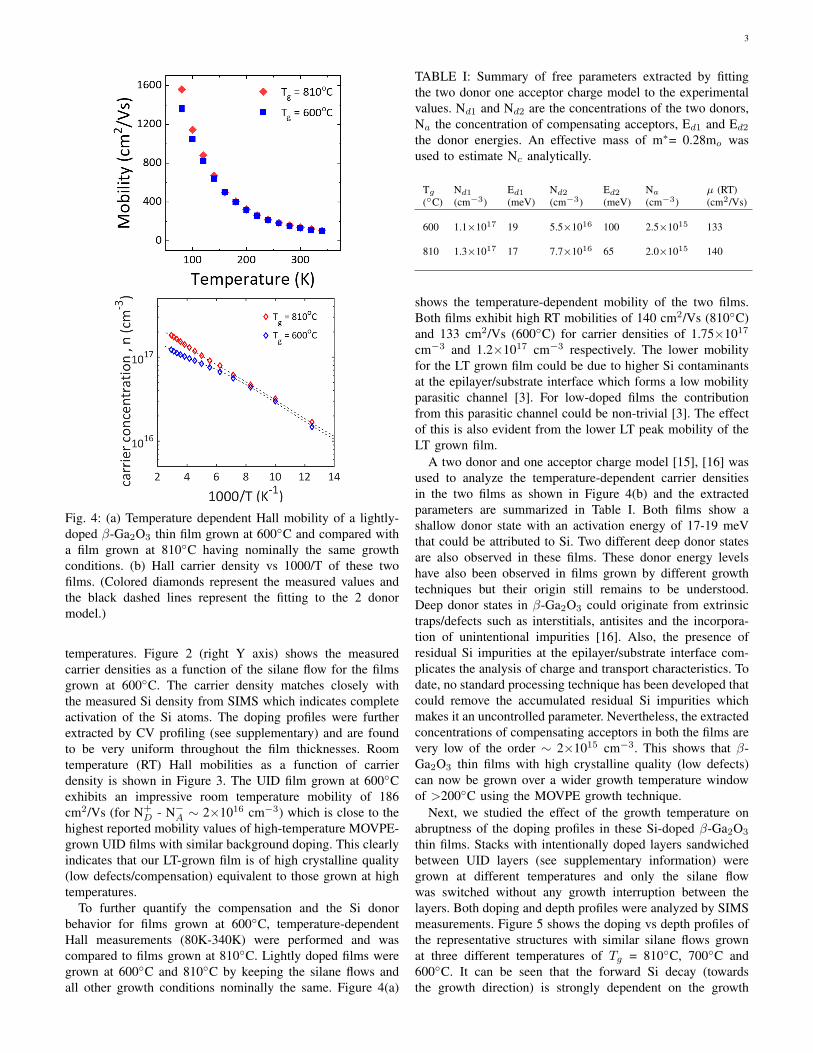
N-type doping is achieved in these films by flowing di-luted silane into the chamber during the growth and dopingin the range of 2×10¹⁶ - 2×1019 cm−3 were studied. Tounderstand the incorporation of Si and other unintentionalimpurities (C, H) in the films grown at 600◦C, secondary-ion mass spectroscopy (SIMS) measurements were done ona stacked structure with different silane flows (see supple-mentary information). Figure 2 shows the measured Si atomdensity (left Y axis) as a function of the silane flow. The Siatom density scales linearly with the silane flow suggestingcomplete incorporation. Impurities such as H and C are alwaysnear the SIMS detection limits at lower silane flows. Thus,high purity β-Ga2O3 thin films with controllable doping areachieved and are further verified by the excellent transport
Fig. 2: Comparison of Si density from SIMS and carrierdensity extracted from Hall measurements in the 600◦C grownβ-Ga2O3 thin films as a function of silane flow.
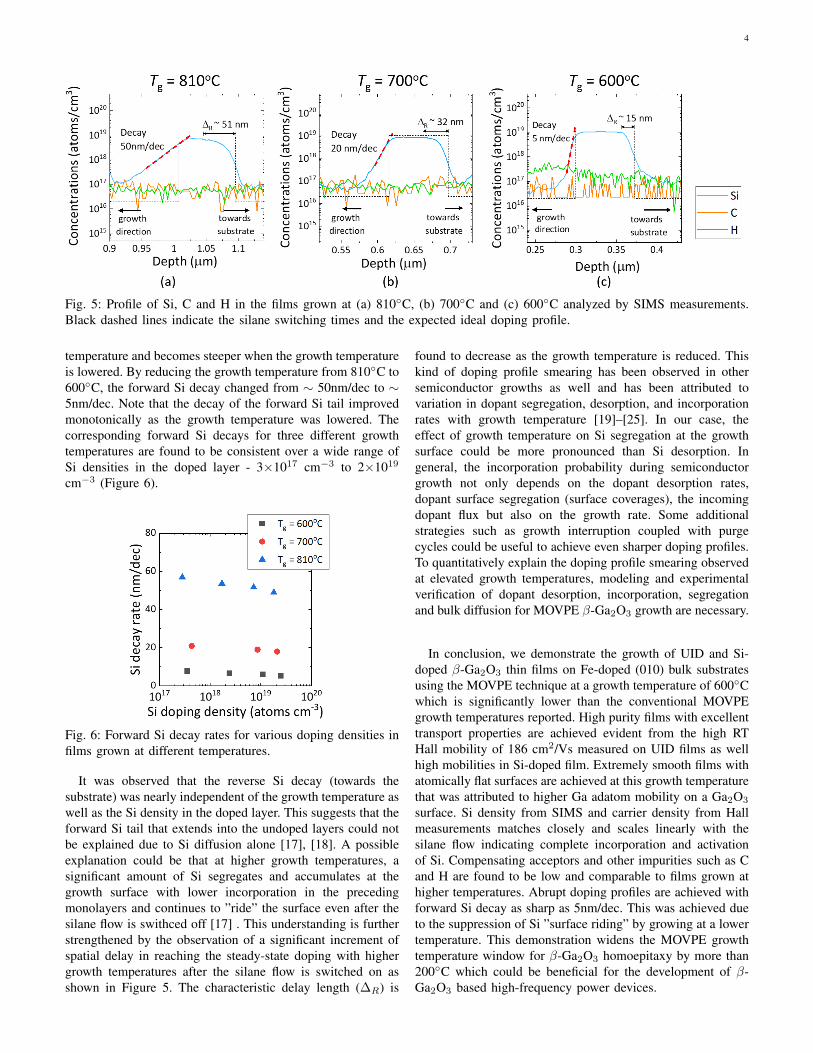
Fig. 3: Room temperature Hall mobility vs carrier density inthe 600◦C grown β-Ga2O3 thin films.
properties as discussed later.Hall effect measurements (Ecopia HMS 7000) were per-
formed to study the transport properties of these films. Ohmiccontacts were formed by depositing Ti (50 nm)/Au (100 nm)on the four corners of as grown unintentionally doped (UID)and Si-doped β-Ga2O3 thin films using DC sputtering. Thecontacts were further annealed in N2 at 450◦C for 1.5 minutesso that the contacts retained their ohmic nature even at low
3
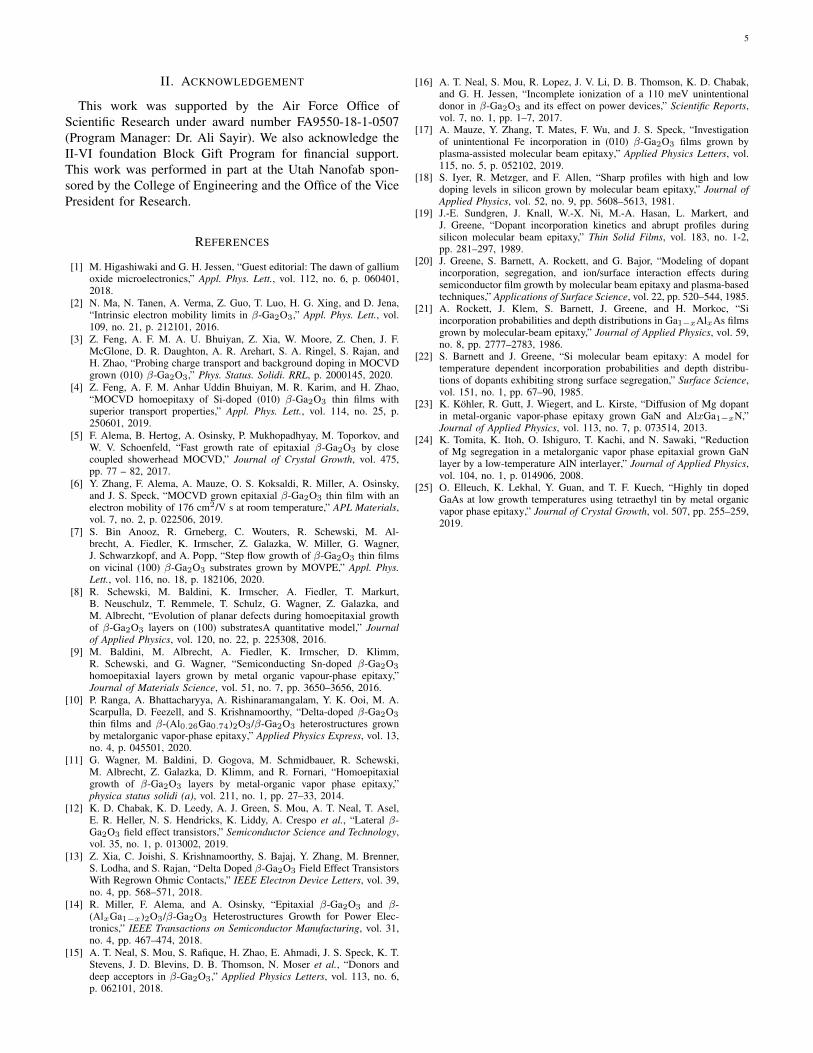
Fig. 4: (a) Temperature dependent Hall mobility of a lightly-doped β-Ga2O3 thin film grown at 600◦C and compared witha film grown at 810◦C having nominally the same growthconditions. (b) Hall carrier density vs 1000/T of these twofilms. (Colored diamonds represent the measured values andthe black dashed lines represent the fitting to the 2 donormodel.)
temperatures. Figure 2 (right Y axis) shows the measuredcarrier densities as a function of the silane flow for the filmsgrown at 600◦C. The carrier density matches closely withthe measured Si density from SIMS which indicates completeactivation of the Si atoms. The doping profiles were furtherextracted by CV profiling (see supplementary) and are foundto be very uniform throughout the film thicknesses. Roomtemperature (RT) Hall mobilities as a function of carrierdensity is shown in Figure 3. The UID film grown at 600◦Cexhibits an impressive room temperature mobility of 186cm2/Vs (for N+
D - N−A ∼ 2×1016 cm−3) which is close to the
highest reported mobility values of high-temperature MOVPE-grown UID films with similar background doping. This clearlyindicates that our LT-grown film is of high crystalline quality(low defects/compensation) equivalent to those grown at hightemperatures.
To further quantify the compensation and the Si donorbehavior for films grown at 600◦C, temperature-dependentHall measurements (80K-340K) were performed and wascompared to films grown at 810◦C. Lightly doped films weregrown at 600◦C and 810◦C by keeping the silane flows andall other growth conditions nominally the same. Figure 4(a)
TABLE I: Summary of free parameters extracted by fittingthe two donor one acceptor charge model to the experimentalvalues. Nd1 and Nd2 are the concentrations of the two donors,Na the concentration of compensating acceptors, Ed1 and Ed2
the donor energies. An effective mass of m∗= 0.28mo wasused to estimate Nc analytically.
Tg Nd1 Ed1 Nd2 Ed2 Na µ (RT)(◦C) (cm−3) (meV) (cm−3) (meV) (cm−3) (cm2/Vs)
600 1.1×10¹⁷ 19 5.5×10¹⁶ 100 2.5×10¹⁵ 133
810 1.3×10¹⁷ 17 7.7×10¹⁶ 65 2.0×10¹⁵ 140
shows the temperature-dependent mobility of the two films.Both films exhibit high RT mobilities of 140 cm2/Vs (810◦C)and 133 cm2/Vs (600◦C) for carrier densities of 1.75×10¹⁷
cm−3 and 1.2×1017 cm−3 respectively. The lower mobilityfor the LT grown film could be due to higher Si contaminantsat the epilayer/substrate interface which forms a low mobilityparasitic channel [3]. For low-doped films the contributionfrom this parasitic channel could be non-trivial [3]. The effectof this is also evident from the lower LT peak mobility of theLT grown film.
A two donor and one acceptor charge model [15], [16] wasused to analyze the temperature-dependent carrier densitiesin the two films as shown in Figure 4(b) and the extractedparameters are summarized in Table I. Both films show ashallow donor state with an activation energy of 17-19 meVthat could be attributed to Si. Two different deep donor statesare also observed in these films. These donor energy levelshave also been observed in films grown by different growthtechniques but their origin still remains to be understood.Deep donor states in β-Ga2O3 could originate from extrinsictraps/defects such as interstitials, antisites and the incorpora-tion of unintentional impurities [16]. Also, the presence ofresidual Si impurities at the epilayer/substrate interface com-plicates the analysis of charge and transport characteristics. Todate, no standard processing technique has been developed thatcould remove the accumulated residual Si impurities whichmakes it an uncontrolled parameter. Nevertheless, the extractedconcentrations of compensating acceptors in both the films arevery low of the order ∼ 2×1015 cm−3. This shows that β-Ga2O3 thin films with high crystalline quality (low defects)can now be grown over a wider growth temperature windowof >200◦C using the MOVPE growth technique.
Next, we studied the effect of the growth temperature onabruptness of the doping profiles in these Si-doped β-Ga2O3
thin films. Stacks with intentionally doped layers sandwichedbetween UID layers (see supplementary information) weregrown at different temperatures and only the silane flowwas switched without any growth interruption between thelayers. Both doping and depth profiles were analyzed by SIMSmeasurements. Figure 5 shows the doping vs depth profiles ofthe representative structures with similar silane flows grownat three different temperatures of Tg = 810◦C, 700◦C and600◦C. It can be seen that the forward Si decay (towardsthe growth direction) is strongly dependent on the growth
4
Fig. 5: Profile of Si, C and H in the films grown at (a) 810◦C, (b) 700◦C and (c) 600◦C analyzed by SIMS measurements.Black dashed lines indicate the silane switching times and the expected ideal doping profile.
temperature and becomes steeper when the growth temperatureis lowered. By reducing the growth temperature from 810◦C to600◦C, the forward Si decay changed from ∼ 50nm/dec to ∼5nm/dec. Note that the decay of the forward Si tail improvedmonotonically as the growth temperature was lowered. Thecorresponding forward Si decays for three different growthtemperatures are found to be consistent over a wide range ofSi densities in the doped layer - 3×1017 cm−3 to 2×10¹⁹
cm−3 (Figure 6).
Fig. 6: Forward Si decay rates for various doping densities infilms grown at different temperatures.
It was observed that the reverse Si decay (towards thesubstrate) was nearly independent of the growth temperature aswell as the Si density in the doped layer. This suggests that theforward Si tail that extends into the undoped layers could notbe explained due to Si diffusion alone [17], [18]. A possibleexplanation could be that at higher growth temperatures, asignificant amount of Si segregates and accumulates at thegrowth surface with lower incorporation in the precedingmonolayers and continues to ”ride” the surface even after thesilane flow is swithced off [17] . This understanding is furtherstrengthened by the observation of a significant increment ofspatial delay in reaching the steady-state doping with highergrowth temperatures after the silane flow is switched on asshown in Figure 5. The characteristic delay length (∆R) is
found to decrease as the growth temperature is reduced. Thiskind of doping profile smearing has been observed in othersemiconductor growths as well and has been attributed tovariation in dopant segregation, desorption, and incorporationrates with growth temperature [19]–[25]. In our case, theeffect of growth temperature on Si segregation at the growthsurface could be more pronounced than Si desorption. Ingeneral, the incorporation probability during semiconductorgrowth not only depends on the dopant desorption rates,dopant surface segregation (surface coverages), the incomingdopant flux but also on the growth rate. Some additionalstrategies such as growth interruption coupled with purgecycles could be useful to achieve even sharper doping profiles.To quantitatively explain the doping profile smearing observedat elevated growth temperatures, modeling and experimentalverification of dopant desorption, incorporation, segregationand bulk diffusion for MOVPE β-Ga2O3 growth are necessary.
In conclusion, we demonstrate the growth of UID and Si-doped β-Ga2O3 thin films on Fe-doped (010) bulk substratesusing the MOVPE technique at a growth temperature of 600◦Cwhich is significantly lower than the conventional MOVPEgrowth temperatures reported. High purity films with excellenttransport properties are achieved evident from the high RTHall mobility of 186 cm2/Vs measured on UID films as wellhigh mobilities in Si-doped film. Extremely smooth films withatomically flat surfaces are achieved at this growth temperaturethat was attributed to higher Ga adatom mobility on a Ga2O3
surface. Si density from SIMS and carrier density from Hallmeasurements matches closely and scales linearly with thesilane flow indicating complete incorporation and activationof Si. Compensating acceptors and other impurities such as Cand H are found to be low and comparable to films grown athigher temperatures. Abrupt doping profiles are achieved withforward Si decay as sharp as 5nm/dec. This was achieved dueto the suppression of Si ”surface riding” by growing at a lowertemperature. This demonstration widens the MOVPE growthtemperature window for β-Ga2O3 homoepitaxy by more than200◦C which could be beneficial for the development of β-Ga2O3 based high-frequency power devices.
5
II. ACKNOWLEDGEMENT
This work was supported by the Air Force Office ofScientific Research under award number FA9550-18-1-0507(Program Manager: Dr. Ali Sayir). We also acknowledge theII-VI foundation Block Gift Program for financial support.This work was performed in part at the Utah Nanofab spon-sored by the College of Engineering and the Office of the VicePresident for Research.
REFERENCES
[1] M. Higashiwaki and G. H. Jessen, “Guest editorial: The dawn of galliumoxide microelectronics,” Appl. Phys. Lett., vol. 112, no. 6, p. 060401,2018.
[2] N. Ma, N. Tanen, A. Verma, Z. Guo, T. Luo, H. G. Xing, and D. Jena,“Intrinsic electron mobility limits in β-Ga2O3,” Appl. Phys. Lett., vol.109, no. 21, p. 212101, 2016.
[3] Z. Feng, A. F. M. A. U. Bhuiyan, Z. Xia, W. Moore, Z. Chen, J. F.McGlone, D. R. Daughton, A. R. Arehart, S. A. Ringel, S. Rajan, andH. Zhao, “Probing charge transport and background doping in MOCVDgrown (010) β-Ga2O3,” Phys. Status. Solidi. RRL, p. 2000145, 2020.
[4] Z. Feng, A. F. M. Anhar Uddin Bhuiyan, M. R. Karim, and H. Zhao,“MOCVD homoepitaxy of Si-doped (010) β-Ga2O3 thin films withsuperior transport properties,” Appl. Phys. Lett., vol. 114, no. 25, p.250601, 2019.
[5] F. Alema, B. Hertog, A. Osinsky, P. Mukhopadhyay, M. Toporkov, andW. V. Schoenfeld, “Fast growth rate of epitaxial β-Ga2O3 by closecoupled showerhead MOCVD,” Journal of Crystal Growth, vol. 475,pp. 77 – 82, 2017.
[6] Y. Zhang, F. Alema, A. Mauze, O. S. Koksaldi, R. Miller, A. Osinsky,and J. S. Speck, “MOCVD grown epitaxial β-Ga2O3 thin film with anelectron mobility of 176 cm2/V s at room temperature,” APL Materials,vol. 7, no. 2, p. 022506, 2019.
[7] S. Bin Anooz, R. Grneberg, C. Wouters, R. Schewski, M. Al-brecht, A. Fiedler, K. Irmscher, Z. Galazka, W. Miller, G. Wagner,J. Schwarzkopf, and A. Popp, “Step flow growth of β-Ga2O3 thin filmson vicinal (100) β-Ga2O3 substrates grown by MOVPE,” Appl. Phys.Lett., vol. 116, no. 18, p. 182106, 2020.
[8] R. Schewski, M. Baldini, K. Irmscher, A. Fiedler, T. Markurt,B. Neuschulz, T. Remmele, T. Schulz, G. Wagner, Z. Galazka, andM. Albrecht, “Evolution of planar defects during homoepitaxial growthof β-Ga2O3 layers on (100) substratesA quantitative model,” Journalof Applied Physics, vol. 120, no. 22, p. 225308, 2016.
[9] M. Baldini, M. Albrecht, A. Fiedler, K. Irmscher, D. Klimm,R. Schewski, and G. Wagner, “Semiconducting Sn-doped β-Ga2O3
homoepitaxial layers grown by metal organic vapour-phase epitaxy,”Journal of Materials Science, vol. 51, no. 7, pp. 3650–3656, 2016.
[10] P. Ranga, A. Bhattacharyya, A. Rishinaramangalam, Y. K. Ooi, M. A.Scarpulla, D. Feezell, and S. Krishnamoorthy, “Delta-doped β-Ga2O3
thin films and β-(Al0.26Ga0.74)2O3/β-Ga2O3 heterostructures grownby metalorganic vapor-phase epitaxy,” Applied Physics Express, vol. 13,no. 4, p. 045501, 2020.
[11] G. Wagner, M. Baldini, D. Gogova, M. Schmidbauer, R. Schewski,M. Albrecht, Z. Galazka, D. Klimm, and R. Fornari, “Homoepitaxialgrowth of β-Ga2O3 layers by metal-organic vapor phase epitaxy,”physica status solidi (a), vol. 211, no. 1, pp. 27–33, 2014.
[12] K. D. Chabak, K. D. Leedy, A. J. Green, S. Mou, A. T. Neal, T. Asel,E. R. Heller, N. S. Hendricks, K. Liddy, A. Crespo et al., “Lateral β-Ga2O3 field effect transistors,” Semiconductor Science and Technology,vol. 35, no. 1, p. 013002, 2019.
[13] Z. Xia, C. Joishi, S. Krishnamoorthy, S. Bajaj, Y. Zhang, M. Brenner,S. Lodha, and S. Rajan, “Delta Doped β-Ga2O3 Field Effect TransistorsWith Regrown Ohmic Contacts,” IEEE Electron Device Letters, vol. 39,no. 4, pp. 568–571, 2018.
[14] R. Miller, F. Alema, and A. Osinsky, “Epitaxial β-Ga2O3 and β-(AlxGa1−x)2O3/β-Ga2O3 Heterostructures Growth for Power Elec-tronics,” IEEE Transactions on Semiconductor Manufacturing, vol. 31,no. 4, pp. 467–474, 2018.
[15] A. T. Neal, S. Mou, S. Rafique, H. Zhao, E. Ahmadi, J. S. Speck, K. T.Stevens, J. D. Blevins, D. B. Thomson, N. Moser et al., “Donors anddeep acceptors in β-Ga2O3,” Applied Physics Letters, vol. 113, no. 6,p. 062101, 2018.
[16] A. T. Neal, S. Mou, R. Lopez, J. V. Li, D. B. Thomson, K. D. Chabak,and G. H. Jessen, “Incomplete ionization of a 110 meV unintentionaldonor in β-Ga2O3 and its effect on power devices,” Scientific Reports,vol. 7, no. 1, pp. 1–7, 2017.
[17] A. Mauze, Y. Zhang, T. Mates, F. Wu, and J. S. Speck, “Investigationof unintentional Fe incorporation in (010) β-Ga2O3 films grown byplasma-assisted molecular beam epitaxy,” Applied Physics Letters, vol.115, no. 5, p. 052102, 2019.
[18] S. Iyer, R. Metzger, and F. Allen, “Sharp profiles with high and lowdoping levels in silicon grown by molecular beam epitaxy,” Journal ofApplied Physics, vol. 52, no. 9, pp. 5608–5613, 1981.
[19] J.-E. Sundgren, J. Knall, W.-X. Ni, M.-A. Hasan, L. Markert, andJ. Greene, “Dopant incorporation kinetics and abrupt profiles duringsilicon molecular beam epitaxy,” Thin Solid Films, vol. 183, no. 1-2,pp. 281–297, 1989.
[20] J. Greene, S. Barnett, A. Rockett, and G. Bajor, “Modeling of dopantincorporation, segregation, and ion/surface interaction effects duringsemiconductor film growth by molecular beam epitaxy and plasma-basedtechniques,” Applications of Surface Science, vol. 22, pp. 520–544, 1985.
[21] A. Rockett, J. Klem, S. Barnett, J. Greene, and H. Morkoc, “Siincorporation probabilities and depth distributions in Ga1−xAlxAs filmsgrown by molecular-beam epitaxy,” Journal of Applied Physics, vol. 59,no. 8, pp. 2777–2783, 1986.
[22] S. Barnett and J. Greene, “Si molecular beam epitaxy: A model fortemperature dependent incorporation probabilities and depth distribu-tions of dopants exhibiting strong surface segregation,” Surface Science,vol. 151, no. 1, pp. 67–90, 1985.
[23] K. Kohler, R. Gutt, J. Wiegert, and L. Kirste, “Diffusion of Mg dopantin metal-organic vapor-phase epitaxy grown GaN and AlxGa1−xN,”Journal of Applied Physics, vol. 113, no. 7, p. 073514, 2013.
[24] K. Tomita, K. Itoh, O. Ishiguro, T. Kachi, and N. Sawaki, “Reductionof Mg segregation in a metalorganic vapor phase epitaxial grown GaNlayer by a low-temperature AlN interlayer,” Journal of Applied Physics,vol. 104, no. 1, p. 014906, 2008.
[25] O. Elleuch, K. Lekhal, Y. Guan, and T. F. Kuech, “Highly tin dopedGaAs at low growth temperatures using tetraethyl tin by metal organicvapor phase epitaxy,” Journal of Crystal Growth, vol. 507, pp. 255–259,2019.