High Speed Optocoupler, 5 MBd, 1 kV/μs dV/dtHigh Speed Optocoupler, 5 MBd, 1 kV/μs dV/dt ......
16
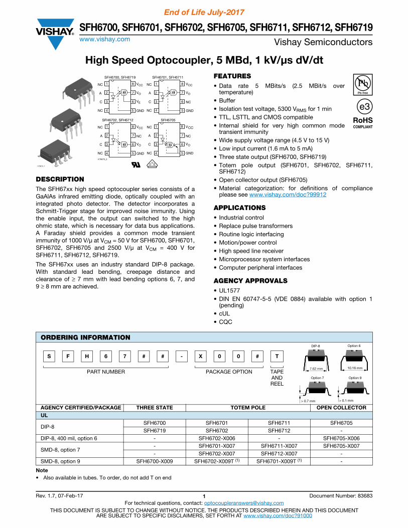
SFH6700, SFH6701, SFH6702, SFH6705, SFH6711, SFH6712, SFH6719 www.vishay.com Vishay Semiconductors End of Life July-2017 Rev. 1.7, 07-Feb-17 1 Document Number: 83683 For technical questions, contact: [email protected] THIS DOCUMENT IS SUBJECT TO CHANGE WITHOUT NOTICE. THE PRODUCTS DESCRIBED HEREIN AND THIS DOCUMENT ARE SUBJECT TO SPECIFIC DISCLAIMERS, SET FORTH AT www.vishay.com/doc?91000 High Speed Optocoupler, 5 MBd, 1 kV/μs dV/dt DESCRIPTION The SFH67xx high speed optocoupler series consists of a GaAlAs infrared emitting diode, optically coupled with an integrated photo detector. The detector incorporates a Schmitt-Trigger stage for improved noise immunity. Using the enable input, the output can switched to the high ohmic state, which is necessary for data bus applications. A Faraday shield provides a common mode transient immunity of 1000 V/μ at V CM = 50 V for SFH6700, SFH6701, SFH6702, SFH6705 and 2500 V/μ at V CM = 400 V for SFH6711, SFH6712, SFH6719. The SFH67xx uses an industry standard DIP-8 package. With standard lead bending, creepage distance and clearance of ≥ 7 mm with lead bending options 6, 7, and 9 ≥ 8 mm are achieved. FEATURES • Data rate 5 MBits/s (2.5 MBit/s over temperature) • Buffer • Isolation test voltage, 5300 V RMS for 1 min • TTL, LSTTL and CMOS compatible • Internal shield for very high common mode transient immunity • Wide supply voltage range (4.5 V to 15 V) • Low input current (1.6 mA to 5 mA) • Three state output (SFH6700, SFH6719) • Totem pole output (SFH6701, SFH6702, SFH6711, SFH6712) • Open collector output (SFH6705) • Material categorization: for definitions of compliance please see www.vishay.com/doc?99912 APPLICATIONS • Industrial control • Replace pulse transformers • Routine logic interfacing • Motion/power control • High speed line receiver • Microprocessor system interfaces • Computer peripheral interfaces AGENCY APPROVALS • UL1577 • DIN EN 60747-5-5 (VDE 0884) available with option 1 (pending) • cUL • CQC Note • Also available in tubes. To order, do not add T on end i179073_2 1 2 3 4 8 7 6 5 V CC V O V E GND NC A C NC SFH6700, SFH6719 1 2 3 4 8 7 6 5 V CC V O NC GND NC A C NC SFH6701, SFH6711 SFH6702, SFH6712 1 2 3 4 8 7 6 5 V CC NC V O GND SFH6705 NC A C NC 1 2 3 4 8 7 6 5 V CC NC V O GND NC A C NC V D E i179073_7 ORDERING INFORMATION S F H 6 7 # # - X 0 0 # T PART NUMBER PACKAGE OPTION TAPE AND REEL AGENCY CERTIFIED/PACKAGE THREE STATE TOTEM POLE OPEN COLLECTOR UL DIP-8 SFH6700 SFH6701 SFH6711 SFH6705 SFH6719 SFH6702 SFH6712 - DIP-8, 400 mil, option 6 - SFH6702-X006 - SFH6705-X006 SMD-8, option 7 - SFH6701-X007 SFH6711-X007 SFH6705-X007 - SFH6702-X007 SFH6712-X007 - SMD-8, option 9 SFH6700-X009 SFH6702-X009T (1) SFH6701-X009T (1) - > 0.1 mm 10.16 mm > 0.7 mm 7.62 mm DIP-8 Option 7 Option 6 Option 9
Transcript of High Speed Optocoupler, 5 MBd, 1 kV/μs dV/dtHigh Speed Optocoupler, 5 MBd, 1 kV/μs dV/dt ......
SFH6700, SFH6701, SFH6702, SFH6705, SFH6711, SFH6712, SFH6719www.vishay.com Vishay Semiconductors
End of Life July-2017
Rev. 1.7, 07-Feb-17 1 Document Number: 83683For technical questions, contact: [email protected]
THIS DOCUMENT IS SUBJECT TO CHANGE WITHOUT NOTICE. THE PRODUCTS DESCRIBED HEREIN AND THIS DOCUMENTARE SUBJECT TO SPECIFIC DISCLAIMERS, SET FORTH AT www.vishay.com/doc?91000
High Speed Optocoupler, 5 MBd, 1 kV/μs dV/dt
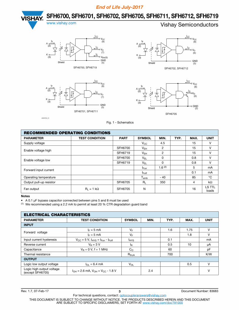
DESCRIPTIONThe SFH67xx high speed optocoupler series consists of a GaAlAs infrared emitting diode, optically coupled with an integrated photo detector. The detector incorporates a Schmitt-Trigger stage for improved noise immunity. Using the enable input, the output can switched to the high ohmic state, which is necessary for data bus applications. A Faraday shield provides a common mode transient immunity of 1000 V/μ at VCM = 50 V for SFH6700, SFH6701, SFH6702, SFH6705 and 2500 V/μ at VCM = 400 V for SFH6711, SFH6712, SFH6719.
The SFH67xx uses an industry standard DIP-8 package. With standard lead bending, creepage distance and clearance of ≥ 7 mm with lead bending options 6, 7, and 9 ≥ 8 mm are achieved.
FEATURES• Data rate 5 MBits/s (2.5 MBit/s over
temperature)• Buffer• Isolation test voltage, 5300 VRMS for 1 min• TTL, LSTTL and CMOS compatible• Internal shield for very high common mode
transient immunity• Wide supply voltage range (4.5 V to 15 V)• Low input current (1.6 mA to 5 mA)• Three state output (SFH6700, SFH6719)• Totem pole output (SFH6701, SFH6702, SFH6711,
SFH6712)• Open collector output (SFH6705)• Material categorization: for definitions of compliance
please see www.vishay.com/doc?99912
APPLICATIONS• Industrial control• Replace pulse transformers• Routine logic interfacing• Motion/power control• High speed line receiver• Microprocessor system interfaces• Computer peripheral interfaces
AGENCY APPROVALS• UL1577• DIN EN 60747-5-5 (VDE 0884) available with option 1
(pending)• cUL• CQC
Note• Also available in tubes. To order, do not add T on end
i179073_2
1
2
3
4
8
7
6
5
VCC
VO
VE
GND
NC
A
C
NC
SFH6700, SFH6719
1
2
3
4
8
7
6
5
VCC
VO
NC
GND
NC
A
C
NC
SFH6701, SFH6711
SFH6702, SFH6712
1
2
3
4
8
7
6
5
VCC
NC
VO
GND
SFH6705
NC
A
C
NC
1
2
3
4
8
7
6
5
VCC
NC
VO
GND
NC
A
C
NC
VD Ei179073_7
ORDERING INFORMATION
S F H 6 7 # # - X 0 0 # T
PART NUMBER PACKAGE OPTION TAPE AND REEL
AGENCY CERTIFIED/PACKAGE THREE STATE TOTEM POLE OPEN COLLECTORUL
DIP-8SFH6700 SFH6701 SFH6711 SFH6705SFH6719 SFH6702 SFH6712 -
DIP-8, 400 mil, option 6 - SFH6702-X006 - SFH6705-X006
SMD-8, option 7- SFH6701-X007 SFH6711-X007 SFH6705-X007- SFH6702-X007 SFH6712-X007 -
SMD-8, option 9 SFH6700-X009 SFH6702-X009T (1) SFH6701-X009T (1) -
> 0.1 mm
10.16 mm
> 0.7 mm
7.62 mm
DIP-8
Option 7
Option 6
Option 9
SFH6700, SFH6701, SFH6702, SFH6705, SFH6711, SFH6712, SFH6719www.vishay.com Vishay Semiconductors
End of Life July-2017
Rev. 1.7, 07-Feb-17 2 Document Number: 83683For technical questions, contact: [email protected]
THIS DOCUMENT IS SUBJECT TO CHANGE WITHOUT NOTICE. THE PRODUCTS DESCRIBED HEREIN AND THIS DOCUMENTARE SUBJECT TO SPECIFIC DISCLAIMERS, SET FORTH AT www.vishay.com/doc?91000
Note• Stresses in excess of the absolute maximum ratings can cause permanent damage to the device. Functional operation of the device is not
implied at these or any other conditions in excess of those given in the operational sections of this document. Exposure to absolute maximum ratings for extended periods of the time can adversely affect reliability
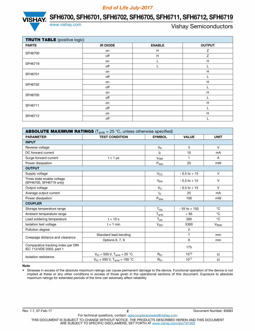
TRUTH TABLE (positive logic)PARTS IR DIODE ENABLE OUTPUT
SFH6700on H Z
off H Z
SFH6719on L H
off L L
SFH6701on H
off L
SFH6702on H
off L
SFH6705on H
off L
SFH6711on H
off L
SFH6712on H
off L
ABSOLUTE MAXIMUM RATINGS (Tamb = 25 °C, unless otherwise specified)PARAMETER TEST CONDITION SYMBOL VALUE UNIT
INPUT
Reverse voltage VR 3 V
DC forward current IF 10 mA
Surge forward current t ≤ 1 μs IFSM 1 A
Power dissipation Pdiss 20 mW
OUTPUT
Supply voltage VCC - 0.5 to + 15 V
Three state enable voltage (SFH6700, SFH6719 only) VEN - 0.5 to + 15 V
Output voltage VO - 0.5 to + 15 V
Average output current IO 25 mA
Power dissipation Pdiss 100 mW
COUPLER
Storage temperature range Tstg - 55 to + 150 °C
Ambient temperature range Tamb + 85 °C
Lead soldering temperature t = 10 s Tsld 260 °C
Isolation test voltage t = 1 min VISO 5300 VRMS
Pollution degree 2
Creepage distance and clearanceStandard lead bending 7 mm
Options 6, 7, 9 8 mm
Comparative tracking index per DIN IEC 112/VDE 0303, part 1 175
Isolation resistanceVIO = 500 V, Tamb = 25 °C RIO 1012 ΩVIO = 500 V, Tamb = 100 °C RIO 1011 Ω
SFH6700, SFH6701, SFH6702, SFH6705, SFH6711, SFH6712, SFH6719www.vishay.com Vishay Semiconductors
End of Life July-2017
Rev. 1.7, 07-Feb-17 3 Document Number: 83683For technical questions, contact: [email protected]
THIS DOCUMENT IS SUBJECT TO CHANGE WITHOUT NOTICE. THE PRODUCTS DESCRIBED HEREIN AND THIS DOCUMENTARE SUBJECT TO SPECIFIC DISCLAIMERS, SET FORTH AT www.vishay.com/doc?91000
Fig. 1 - Schematics
Notes• A 0.1 μF bypass capacitor connected between pins 5 and 8 must be used(1) We recommended using a 2.2 mA to permit at least 20 % CTR degradation guard band
RECOMMENDED OPERATING CONDITIONSPARAMETER TEST CONDITION PART SYMBOL MIN. TYP. MAX. UNIT
Supply voltage VCC 4.5 15 V
Enable voltage highSFH6700 VEH 2 15 V
SFH6719 VEH 2 15 V
Enable voltage lowSFH6700 VEL 0 0.8 V
SFH6719 VEL 0 0.8 V
Forward input currentIFon 1.6 (2) 5 mA
IFoff 0.1 mA
Operating temperature Tamb - 40 85 °C
Output pull-up resistor SFH6705 RL 350 4 kΩ
Fan output RL = 1 kΩ SFH6705 N 16 LS TTLloads
ELECTRICAL CHARACTERISTICSPARAMETER TEST CONDITION SYMBOL MIN. TYP. MAX. UNIT
INPUT
Forward voltageIF = 5 mA VF 1.6 1.75 V
IF = 5 mA VF 1.8 V
Input current hysteresis VCC = 5 V, IHYS = IFon - IFoff IHYS 0.1 mA
Reverse current VR = 3 V IR 0.5 10 μA
Capacitance VR = 0 V, f = 1 MHz CO 60 pF
Thermal resistance RthJA 700 K/W
OUTPUT
Logic low output voltage IOL = 6.4 mA VOL 0.5 V
Logic high output voltage (except SFH6705) IOH = 2.6 mA, VOH = VCC - 1.8 V 2.4 V
isfh6700_01
ICCVCC
VO
IO
IE
IF
VEN(3)
(2)
GNDShield
(8)
(7)
(5)
A
K
SFH6700, SFH6719
(6)
ICCVCC
VO
IO
IF
(3)
(2)
GNDShield
(8)
(6)
(5)
A
K
SFH6702, SFH6712
ICCVCC
VO
IO
IF
(3)
(2)
GNDShield
(8)A
K
(6)
(5)
SFH6705SFH6701, SFH6711
ICCVCC
VO
IO
IF
(3)
(2)
GNDShield
(8)
(7)
(5)
A
K
SFH6700, SFH6701, SFH6702, SFH6705, SFH6711, SFH6712, SFH6719www.vishay.com Vishay Semiconductors
End of Life July-2017
Rev. 1.7, 07-Feb-17 4 Document Number: 83683For technical questions, contact: [email protected]
THIS DOCUMENT IS SUBJECT TO CHANGE WITHOUT NOTICE. THE PRODUCTS DESCRIBED HEREIN AND THIS DOCUMENTARE SUBJECT TO SPECIFIC DISCLAIMERS, SET FORTH AT www.vishay.com/doc?91000
Notes• - 40 °C ≤ Tamb ≤ 85 °C; 4.5 V ≤ VCC ≤ 15 V; 1.6 mA ≤ IFon ≤ 5 mA; 2 ≤ VEH ≤ 15 V; 0 ≤ VEL ≤ 0.8 V; 0 mA ≤ IFoff ≤ 0.1 mA.
Typical values: Tamb = 25 °C; VCC = 5 V; IFon = 3 mA unless otherwise specified. Minimum and maximum values are testing requirements. Typical values are characteristics of the device and are the result of engineering evaluation. Typical values are for information only and are not part of the testing requirements.
(1) Output short circuit time ≤ 10 ms.
OUTPUT
Output leakage current (VOUT > VCC) (except SFH6705)
VO = 5.5 V, VCC = 4.5 V, IF = 5 mA IOHH 0.5 100 μA
VO = 15 V, VCC = 4.5 V, IF = 5 mA IOHH 1 500 μA
Output leakage current (SFH6705 only)
VO = 5.5 V, VCC = 5.5 V, IF = 5 mA IOHH 0.5 100 μA
VO = 15 V, VCC = 15 V, IF = 5 mA IOHH 1 500 μA
Logic high enable voltage (SFH6700/19 only) VEH 2 V
Logic low enable voltage (SFH6700/19 only) VEL 0.8 V
Logic high enable current (SFH6700/19 only)
VEN = 2.7 V IEH 20 μA
VEN = 5.5 V IEH 100 μA
VEN = 15 V IEH 0.001 250 μA
Logic low enable current (SFH6700/19 only) VEN = 0.4 V IEL - 320 - 50 μA
High impedance state output current (SFH6700/19 only)
VO = 0.4 V, VEN = 2 V, IF = 5 mA
IOZL - 20 μA
VO = 2.4 V, VEN = 2 V, IF = 0 mA
IOZH 20 μA
VO = 5.5 V, VEN = 2 V, IF = 0 mA
IOZH 100 μA
IOZH 0.001 500 μA
Logic low supply currentVCC = 5.5 V, IF = 0 ICCL 3.7 6 mA
VCC = 15 V, IF = 0 ICCL 4.1 6.5 mA
Logic high supply currentVCC = 5.5 V, IF = 5 mA ICCH 3.4 4 mA
VCC = 15 V, IF = 5 mA ICCH 3.7 5 mA
Logic low short circuit output current (1)
VO = VCC = 5.5 V, IF = 0 IOSL 25 mA
VO = VCC = 15 V, IF = 0 IOSL 40 mA
Logic high short circuit output current (1)
VCC = 5.5 V, VO = 0 V, IF = 5 IOSL - 10 mA
VCC = 15 V, VO = 0 V, IF = 5 IOSL - 25 mA
Thermal resistance RthJA 300 K/W
COUPLER
Capacitance (input to output) f = 1 MHz, pins 1 to 4 and 5 to 8shorted together CIO 0.6 pF
Isolation resistanceVIO = 500 V, Tamb = 25 °C RIO 1012 Ω
VIO = 500 V, Tamb = 100 °C RIO 1011 Ω
SWITCHING CHARACTERISTICSPARAMETER TEST CONDITION PART SYMBOL MIN. TYP. MAX. UNIT
Propagation delay time to logic low output level, SFH6700, SFH6701, SFH6702, SFH6711, SFH6712, SFH6719 (1)
Without peaking capacitor tPHL 120 ns
With peaking capacitor
tPHL 115 300 ns
tPLH 125 ns
tPLH 90 300 ns
Output enable time to logic high (SFH6700, SFH6719) (1) tPZH 20 ns
Output enable time to logic low (SFH6700, SFH6719) (1) tPZL 25 ns
ELECTRICAL CHARACTERISTICSPARAMETER TEST CONDITION SYMBOL MIN. TYP. MAX. UNIT
SFH6700, SFH6701, SFH6702, SFH6705, SFH6711, SFH6712, SFH6719www.vishay.com Vishay Semiconductors
End of Life July-2017
Rev. 1.7, 07-Feb-17 5 Document Number: 83683For technical questions, contact: [email protected]
THIS DOCUMENT IS SUBJECT TO CHANGE WITHOUT NOTICE. THE PRODUCTS DESCRIBED HEREIN AND THIS DOCUMENTARE SUBJECT TO SPECIFIC DISCLAIMERS, SET FORTH AT www.vishay.com/doc?91000
Notes• 0 °C ≤ Tamb ≤ 85 °C; 4.5 V ≤ VCC ≤ 15 V; 1.6 mA ≤ IFon ≤ 5 mA; 2 ≤ VEH ≤ 15 V (SFH6700/19); 0 ≤ VEL ≤ 0.8 V (SFH6700, SFH6719);
0 mA ≤ IFoff ≤ 0.1 mA(1) Typical values: Tamb = 25 °C; VCC = 5 V; IFon = 3 mA unless otherwise specified (4) (2) Typical values: Tamb = 25 °C, VCC = 5 V; IFon = 3 mA; RL = 390 Ω unless otherwise specified (4) (3) A 0.1 μF bypass capacitor connected between pins 5 and 8 must be used
Notes• Tamb = 25 °C, VCC = 5 V(1) CMH is the maximum slew rate of a common mode voltage VCM at which the output voltage remains at logic high level (VO > 2 V)(2) CML is the maximum slew rate of a common mode voltage VCM at which the output voltage remains at logic high level (VO < 0.8 V)
Output disable time from logic low (SFH6700, SFH6719) (1) tPLZ 50 ns
Output rise time (1) 10 % to 90 % tr 40 ns
Output fall time (1) 90 % to 10 % tf 10 ns
Propagation delay time to logic low output level (3)
Without peaking capacitor SFH6705 tPHL 115 ns
With peaking capacitor SFH6705 tPHL 105 300 ns
Without peaking capacitor SFH6705 tPLH 125 ns
With peaking capacitor SFH6705 tPLH 90 300 ns
Output rise time (3)10 % to 90 % tr 25 ns
90 % to 10 % tr 4 ns
COMMON MODE TRANSIENT IMMUNITYPARAMETER TEST CONDITION PART SYMBOL MIN. TYP. MAX. UNIT
Logic high common mode transient immunity
|VCM| = 50 V, IF = 1.6 mA
SFH6700 |CMH| (1) 1000 V/μs
SFH6701 |CMH| (1) 1000 V/μs
SFH6702 |CMH| (1) 1000 V/μs
SFH6705 |CMH| (1) 1000 V/μs
|VCM| = 400 V, IF = 1.6 mA
SFH6711 |CMH| (1) 2500 V/μs
SFH6712 |CMH| (1) 2500 V/μs
SFH6719 |CMH| (1) 2500 V/μs
Logic Low common mode transient immunity
|VCM| = 50 V, IF = 0 mA SFH6700 |CML| (2) 1000 V/μs
|VCM| = 50 V, IF = 0 mA
SFH6701 |CML| (2) 1000 V/μs
SFH6702 |CML| (2) 1000 V/μs
SFH6705 |CML| (2) 1000 V/μs
|VCM| = 400 V, IF = 0 mA
SFH6711 |CML| (2) 2500 V/μs
SFH6712 |CML| (2) 2500 V/μs
SFH6719 |CML| (2) 2500 V/μs
SWITCHING CHARACTERISTICSPARAMETER TEST CONDITION PART SYMBOL MIN. TYP. MAX. UNIT
SFH6700, SFH6701, SFH6702, SFH6705, SFH6711, SFH6712, SFH6719www.vishay.com Vishay Semiconductors
End of Life July-2017
Rev. 1.7, 07-Feb-17 6 Document Number: 83683For technical questions, contact: [email protected]
THIS DOCUMENT IS SUBJECT TO CHANGE WITHOUT NOTICE. THE PRODUCTS DESCRIBED HEREIN AND THIS DOCUMENTARE SUBJECT TO SPECIFIC DISCLAIMERS, SET FORTH AT www.vishay.com/doc?91000
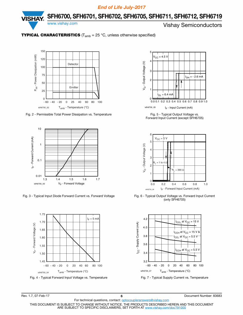
TYPICAL CHARACTERISTICS (Tamb = 25 °C, unless otherwise specified)
Fig. 2 - Permissible Total Power Dissipation vs. Temperature
Fig. 3 - Typical Input Diode Forward Current vs. Forward Voltage
Fig. 4 - Typical Forward Input Voltage vs. Temperature
Fig. 5 - Typical Output Voltage vs.Forward Input Current (except SFH6705)
Fig. 6 - Typical Output Voltage vs. Forward Input Current(only SFH6705)
Fig. 7 - Typical Supply Current vs. Temperature
isfh6700_02 Tamb - Temperature (°C)
Emitter
Detector
150
120
100
75
50
25
0- 60 - 40 - 20 0 25 40 60 80 100
Pto
t - P
ower
Dis
sipa
tion
(mW
)
isfh6700_03 VF - Forward Voltage
I F -
For
war
d C
urre
nt (
mA
)
0.01
0.1
1
10
1.3 1.4 1.5 1.6 1.7
isfh6700_04
- 60 - 40 - 20 0 20 40 60 80 100
1.45
1.50
1.55
1.60
1.65
1.70
1.75
VF -
For
war
d V
olta
ge (
V)
IF = 5 mA
Tamb - Temperature (°C)
isfh6700_05
0
1
2
3
4
5
IF - Input Current (mA)
VO
- O
utpu
t Vol
tage
(V
)
IOL = 6.4 mA
IOH = - 2.6 mA
VCC = 4.5 V
0.0 0.1 0.2 0.3 0.4 0.5 0.6 0.7 0.8 0.9 1.0
isfh6700_06
0
1
2
3
4
5
6
0.0 0.2 0.4 0.6 0.8 1.0
IF - Forward Input Current (mA)
VO
- O
utpu
t Vol
tage
(V
)
RL = 1 to 4 Ω
VCC = 5 V
RL = 390 Ω
isfh6700_07
- 60 - 40 - 20 0 20 40 60 80 100 3.2
3.4
3.6
3.8
4.0
ICCL at VCC = 15 V
ICCH at VCC = 15 V &
ICCL at VCC = 5.5 V
ICCH at VCC = 5.5 V
Tamb - Temperature (°C)
4.2
I CC
- S
uppl
y C
urre
nt (
mA
)
SFH6700, SFH6701, SFH6702, SFH6705, SFH6711, SFH6712, SFH6719www.vishay.com Vishay Semiconductors
End of Life July-2017
Rev. 1.7, 07-Feb-17 7 Document Number: 83683For technical questions, contact: [email protected]
THIS DOCUMENT IS SUBJECT TO CHANGE WITHOUT NOTICE. THE PRODUCTS DESCRIBED HEREIN AND THIS DOCUMENTARE SUBJECT TO SPECIFIC DISCLAIMERS, SET FORTH AT www.vishay.com/doc?91000
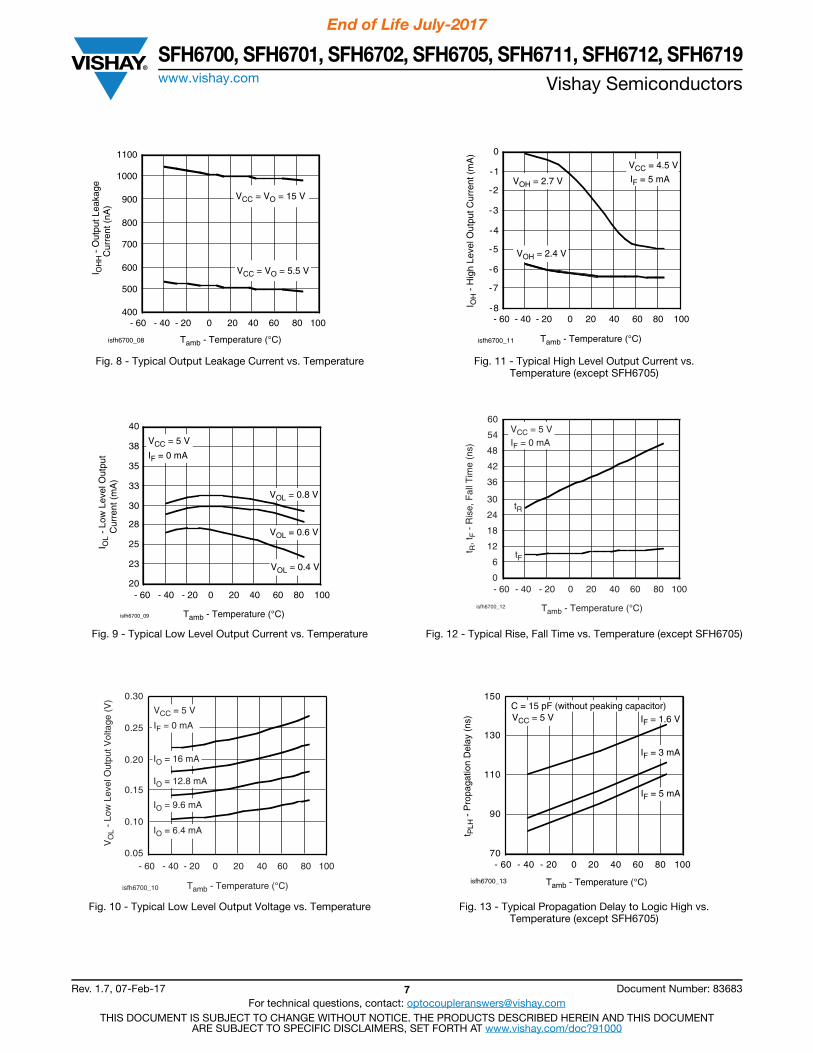
Fig. 8 - Typical Output Leakage Current vs. Temperature
Fig. 9 - Typical Low Level Output Current vs. Temperature
Fig. 10 - Typical Low Level Output Voltage vs. Temperature
Fig. 11 - Typical High Level Output Current vs.Temperature (except SFH6705)
Fig. 12 - Typical Rise, Fall Time vs. Temperature (except SFH6705)
Fig. 13 - Typical Propagation Delay to Logic High vs.Temperature (except SFH6705)
isfh6700_08
400
500
600
700
800
900
1000
1100
- 60 - 40 - 20 0 20 40 60 80 100
I OH
H -
Out
put L
eaka
ge
C
urre
nt (
nA)
VCC = VO = 15 V
VCC = VO = 5.5 V
Tamb - Temperature (°C)
isfh6700_09
20
23
25
28
30
33
35
38
40
- 60 - 40 - 20 0 20 40 60 80 100
I OL
- Lo
w L
evel
Out
put
Cur
rent
(m
A)
VCC = 5 V
IF = 0 mA
VOL = 0.6 V
VOL = 0.4 V
VOL = 0.8 V
Tamb - Temperature (°C)
isfh6700_10
- 60 - 40 - 20 0 20 40 60 80 100 0.05
0.10
0.15
0.20
0.25
0.30
VO
L -
Low
Lev
el O
utpu
t Vol
tage
(V
)
IO = 16 mA
IO = 12.8 mA
IO = 9.6 mA
IO = 6.4 mA
VCC = 5 V
IF = 0 mA
Tamb - Temperature (°C)
isfh6700_11
- 60 - 40 - 20 0 20 40 60 80 100 -8
-7
-6
-5
-4
-3
-2
-1
0
I OH
- H
igh
Leve
l Out
put C
urre
nt (
mA
)
VOH = 2.4 V
VCC = 4.5 V
IF = 5 mAVOH = 2.7 V
Tamb - Temperature (°C)
isfh6700_12
- 60 - 40 - 20 0 20 40 60 80 100 0
6
12
18
24
30
36
42
48
54
60
t R, t
F -
Ris
e, F
all T
ime
(ns)
tR
tF
VCC = 5 VIF = 0 mA
Tamb - Temperature (°C)
isfh6700_13
- 60 - 40 - 20 0 20 40 60 80 100
t PLH
- P
ropa
gatio
n D
elay
(ns
)
70
90
110
130
150
IF = 3 mA
IF = 5 mA
Tamb - Temperature (°C)
C = 15 pF (without peaking capacitor) VCC = 5 V IF = 1.6 V
SFH6700, SFH6701, SFH6702, SFH6705, SFH6711, SFH6712, SFH6719www.vishay.com Vishay Semiconductors
End of Life July-2017
Rev. 1.7, 07-Feb-17 8 Document Number: 83683For technical questions, contact: [email protected]
THIS DOCUMENT IS SUBJECT TO CHANGE WITHOUT NOTICE. THE PRODUCTS DESCRIBED HEREIN AND THIS DOCUMENTARE SUBJECT TO SPECIFIC DISCLAIMERS, SET FORTH AT www.vishay.com/doc?91000
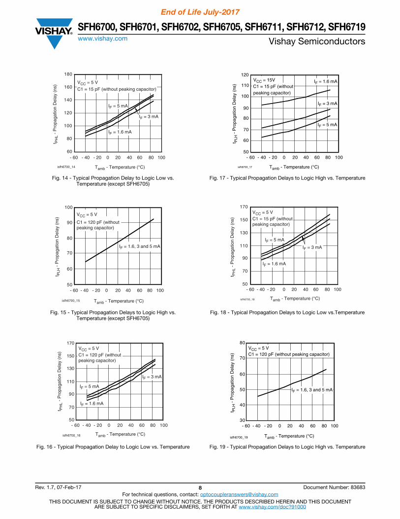
Fig. 14 - Typical Propagation Delay to Logic Low vs.Temperature (except SFH6705)
Fig. 15 - Typical Propagation Delays to Logic High vs.Temperature (except SFH6705)
Fig. 16 - Typical Propagation Delay to Logic Low vs. Temperature
Fig. 17 - Typical Propagation Delays to Logic High vs. Temperature
Fig. 18 - Typical Propagation Delays to Logic Low vs.Temperature
Fig. 19 - Typical Propagation Delays to Logic High vs. Temperature
isfh6700_14
- 60 - 40 - 20 0 20 40 60 80 100
t PH
L -
Pro
paga
tion
Del
ay (
ns)
60
80
100
120
140
160
180
VCC = 5 V
C1 = 15 pF (without peaking capacitor)
IF = 3 mA
IF = 1.6 mA
Tamb - Temperature (°C)
IF = 5 mA
isfh6700_15
- 60 - 40 - 20 0 20 40 60 80 100
t PLH
- P
ropa
gatio
n D
elay
(ns
)
50
60
70
80
90
100
VCC = 5 V
C1 = 120 pF (withoutpeaking capacitor)
IF = 1.6, 3 and 5 mA
Tamb - Temperature (°C)
isfh6700_16
- 60 - 40 - 20 0 20 40 60 80 100
t PH
L -
Pro
paga
tion
Del
ay (
ns)
50
70
90
110
130
150
170VCC = 5 VC1 = 120 pF (withoutpeaking capacitor)
IF = 3 mA
IF = 5 mA
IF = 1.6 mA
Tamb - Temperature (°C)
isfh6700_17
- 60 - 40 - 20 0 20 40 60 80 100
t PLH
- P
ropa
gatio
n D
elay
(ns
)
50
60
70
80
90
VCC = 15VC1 = 15 pF (withoutpeaking capacitor)
IF = 1.6 mA
IF = 3 mA
IF = 5 mA
Tamb - Temperature (°C)
100
110
120
isfh6700_18
- 60 - 40 - 20 0 20 40 60 80 100
t PH
L -
Pro
paga
tion
Del
ay (
ns)
50
70
90
110
130
150
170VCC = 5 VC1 = 15 pF (withoutpeaking capacitor)
IF = 5 mA
IF = 1.6 mA
IF = 3 mA
Tamb - Temperature (°C)
isfh6700_19
- 60 - 40 - 20 0 20 40 60 80 100
t PLH
- P
ropa
gatio
n D
elay
(ns
)
30
40
50
60
70
80VCC = 5 VC1 = 120 pF (without peaking capacitor)
IF = 1.6, 3 and 5 mA
Tamb - Temperature (°C)
SFH6700, SFH6701, SFH6702, SFH6705, SFH6711, SFH6712, SFH6719www.vishay.com Vishay Semiconductors
End of Life July-2017
Rev. 1.7, 07-Feb-17 9 Document Number: 83683For technical questions, contact: [email protected]
THIS DOCUMENT IS SUBJECT TO CHANGE WITHOUT NOTICE. THE PRODUCTS DESCRIBED HEREIN AND THIS DOCUMENTARE SUBJECT TO SPECIFIC DISCLAIMERS, SET FORTH AT www.vishay.com/doc?91000
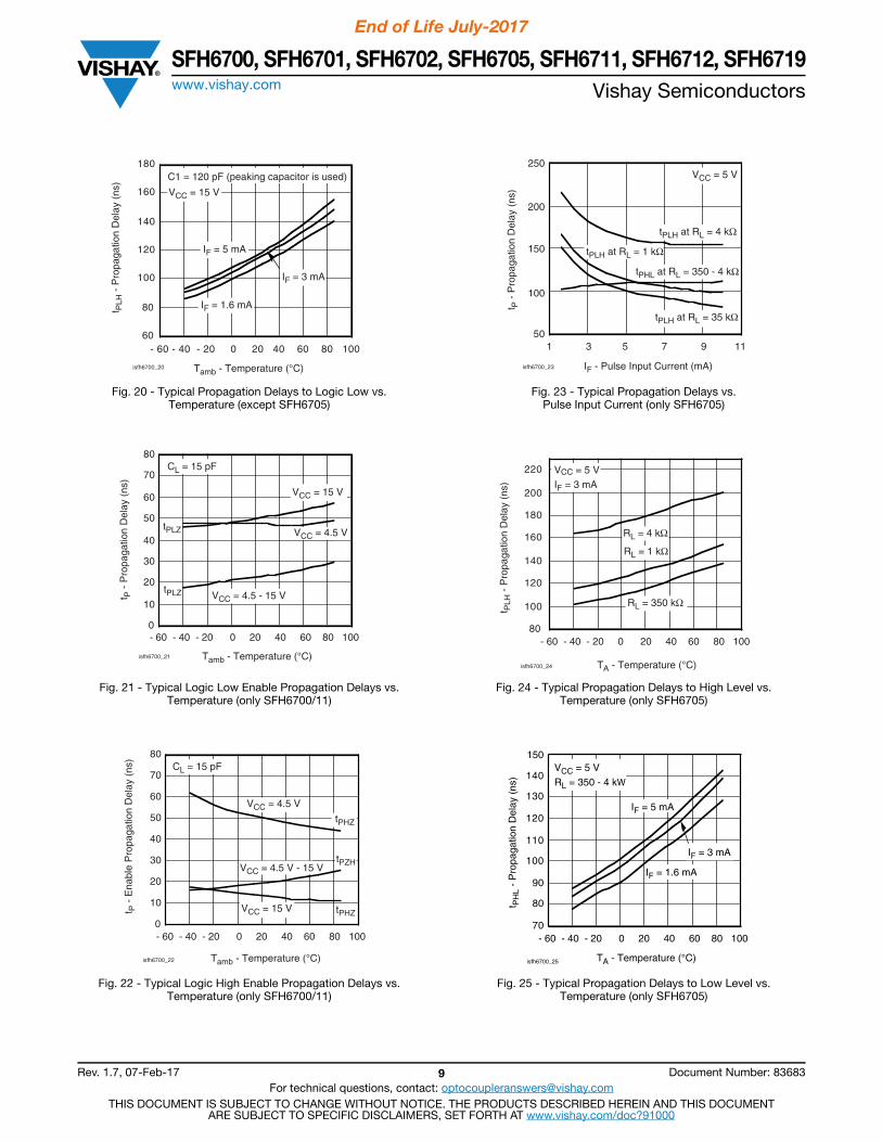
Fig. 20 - Typical Propagation Delays to Logic Low vs.Temperature (except SFH6705)
Fig. 21 - Typical Logic Low Enable Propagation Delays vs.Temperature (only SFH6700/11)
Fig. 22 - Typical Logic High Enable Propagation Delays vs. Temperature (only SFH6700/11)
Fig. 23 - Typical Propagation Delays vs.Pulse Input Current (only SFH6705)
Fig. 24 - Typical Propagation Delays to High Level vs.Temperature (only SFH6705)
Fig. 25 - Typical Propagation Delays to Low Level vs.Temperature (only SFH6705)
isfh6700_20
60
80
100
120
140
160
180
- 60 - 40 - 20 0 20 40 60 80 100
VCC = 15 V
C1 = 120 pF (peaking capacitor is used)
IF = 5 mA
t PLH
- P
ropa
gatio
n D
elay
(ns
)
IF = 3 mA
IF = 1.6 mA
Tamb - Temperature (°C)
isfh6700_21
t P -
Pro
paga
tion
Del
ay (
ns)
0
10
20
30
40
50
60
70
80
- 60 - 40 - 20 0 20 40 60 80 100
CL = 15 pF
VCC = 15 V
VCC = 4.5 - 15 VtPLZ
tPLZ VCC = 4.5 V
Tamb - Temperature (°C)
isfh6700_22
0
10
20
30
40
50
60
70
80
- 60 - 40 - 20 0 20 40 60 80 100
CL = 15 pF
tPHZ
tPZH
tPHZ
VCC = 4.5 V
t P -
Ena
ble
Pro
paga
tion
Del
ay (
ns)
VCC = 4.5 V - 15 V
VCC = 15 V
Tamb - Temperature (°C)
isfh6700_23 IF - Pulse Input Current (mA)
50
100
150
200
250
1 3 5 7 9 11
VCC = 5 V
tPLH at RL = 4 kΩ
t P -
Pro
paga
tion
Del
ay (
ns)
tPHL at RL = 350 - 4 kΩ
tPLH at RL = 35 kΩ
tPLH at RL = 1 kΩ
isfh6700_24
- 60 - 40 - 20 0 20 40 60 80 100
TA - Temperature (°C)
80
100
120
140
160
180
200
220 VCC = 5 VIF = 3 mA
t PLH
- P
ropa
gatio
n D
elay
(ns
)
RL = 4 kΩ
RL = 350 kΩ
RL = 1 kΩ
isfh6700_25
- 60 - 40 - 20 0 20 40 60 80 100
TA - Temperature (°C)
t PH
L -
Pro
paga
tion
Del
ay (
ns)
70
80
90
100
110
120
130
140VCC = 5 VRL = 350 - 4 kW
IF = 5 mA
IF = 3 mA
IF = 1.6 mA
150
SFH6700, SFH6701, SFH6702, SFH6705, SFH6711, SFH6712, SFH6719www.vishay.com Vishay Semiconductors
End of Life July-2017
Rev. 1.7, 07-Feb-17 10 Document Number: 83683For technical questions, contact: [email protected]
THIS DOCUMENT IS SUBJECT TO CHANGE WITHOUT NOTICE. THE PRODUCTS DESCRIBED HEREIN AND THIS DOCUMENTARE SUBJECT TO SPECIFIC DISCLAIMERS, SET FORTH AT www.vishay.com/doc?91000
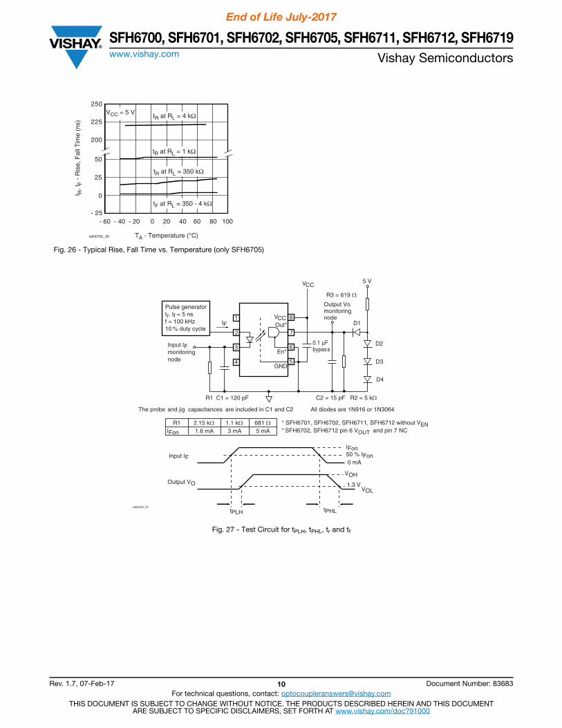
Fig. 26 - Typical Rise, Fall Time vs. Temperature (only SFH6705)
Fig. 27 - Test Circuit for tPLH, tPHL, tr and tf
isfh6700_26
- 25
0
25
50
- 60 - 40 - 20 0 20 40 60 80 100
250
225tR at RL = 4 kΩVCC = 5 V
200
t R, t
F -
Ris
e, F
all T
ime
(ns)
TA - Temperature (°C)
tR at RL = 1 kΩ
tR at RL = 350 kΩ
tF at RL = 350 - 4 kΩ
isfh6700_27
All diodes are 1N916 or 1N3064The probe and jig capacitances are included in C1 and C2
* SFH6701, SFH6702, SFH6711, SFH6712 without VEN* SFH6702, SFH6712 pin 6 VOUT and pin 7 NC
Pulse generatortr, tf = 5 nsf = 100 kHz10 % duty cycle
1
2
3
4
Input IFmonitoringnode
C1 = 120 pF C2 = 15 pF R2 = 5 kΩ
R3 = 619 Ω
VCCOut*
En*
GND
VCC5 V
Output Vomonitoringnode
D1
D2
D3
D4
IF
R1
0.1 µFbypass
8
7
6
5
R1IFon
2.15 kΩ1.6 mA
681 Ω5 mA
1.1 kΩ3 mA
Input IF
Output VO
IFon50 % IFon0 mA
VOH
1.3 V
tPLH tPHL
VOL
SFH6700, SFH6701, SFH6702, SFH6705, SFH6711, SFH6712, SFH6719www.vishay.com Vishay Semiconductors
End of Life July-2017
Rev. 1.7, 07-Feb-17 11 Document Number: 83683For technical questions, contact: [email protected]
THIS DOCUMENT IS SUBJECT TO CHANGE WITHOUT NOTICE. THE PRODUCTS DESCRIBED HEREIN AND THIS DOCUMENTARE SUBJECT TO SPECIFIC DISCLAIMERS, SET FORTH AT www.vishay.com/doc?91000
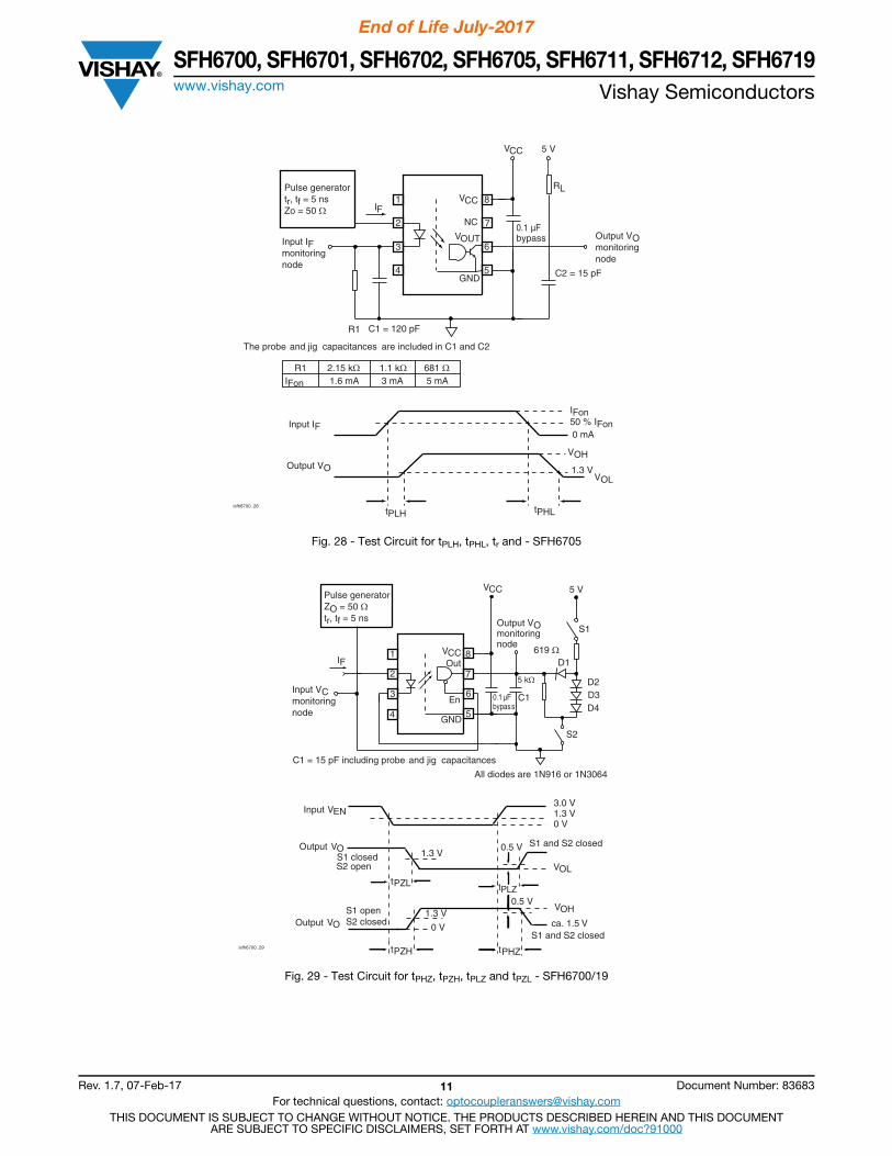
Fig. 28 - Test Circuit for tPLH, tPHL, tr and - SFH6705
Fig. 29 - Test Circuit for tPHZ, tPZH, tPLZ and tPZL - SFH6700/19
isfh6700_28
The probe and jig capacitances are included in C1 and C2
R1IFon
2.15 kΩ1.6 mA
681 Ω5 mA
1.1 kΩ3 mA
Input IF
Output VO
IFon50 % IFon0 mA
VOH
1.3 V
tPLH tPHL
VOL
1
2
3
4 C2 = 15 pFGND
0.1 µFbypass
8
7
6
5
C1 = 120 pF
VCC
VOUT
VCC
IF
R1
RL
5 V
NC
Input IFmonitoringnode
Output VOmonitoringnode
Pulse generatortr, tf = 5 nsZo = 50 Ω
isfh6700_29
Output VO
VOL
Output VO
VOH
tPZL tPLZ
S1 and S2 closed
S1 closedS2 open
1.3 V0.5 V
S1 and S2 closedca. 1.5 V
S1 openS2 closed
tPZH tPHZ
1.3 V
0 V
0.5 V
Input VEN3.0 V1.3 V0 V
1
2
3
4
6
7
8VCCOut
En
GND
VCC 5 V
D1
D2D3D4
All diodes are 1N916 or 1N3064
IF619 Ω
C1
S1
S2
C1 = 15 pF including probe and jig capacitances
5 kΩ
0.1 µFbypass
Pulse generatorZO = 50 Ωtr, tf = 5 ns
Input VCmonitoringnode
Output VOmonitoringnode
5
SFH6700, SFH6701, SFH6702, SFH6705, SFH6711, SFH6712, SFH6719www.vishay.com Vishay Semiconductors
End of Life July-2017
Rev. 1.7, 07-Feb-17 12 Document Number: 83683For technical questions, contact: [email protected]
THIS DOCUMENT IS SUBJECT TO CHANGE WITHOUT NOTICE. THE PRODUCTS DESCRIBED HEREIN AND THIS DOCUMENTARE SUBJECT TO SPECIFIC DISCLAIMERS, SET FORTH AT www.vishay.com/doc?91000
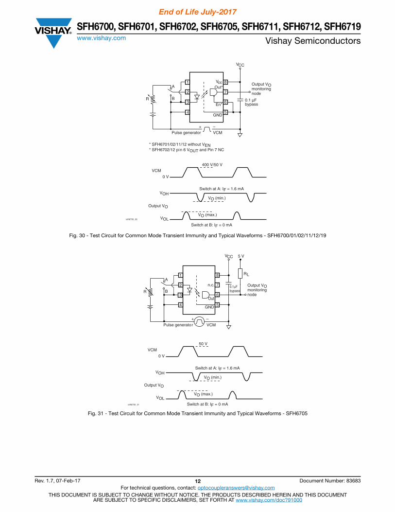
Fig. 30 - Test Circuit for Common Mode Transient Immunity and Typical Waveforms - SFH6700/01/02/11/12/19
Fig. 31 - Test Circuit for Common Mode Transient Immunity and Typical Waveforms - SFH6705
isfh6700_30
0.1 µFbypass
Output VOmonitoringnode
1
2
3
4
6
7
8VccOut*
En*
GND
VCC
A
BR
Pulse generator+ –
VCM
* SFH6701/02/11/12 without VEN* SFH6702/12 pin 6 VOUT and Pin 7 NC
5
Output VO
VCM400 V/50 V
Switch at A: IF = 1.6 mA
0 V
VOHVO (min.)
VOLVO (max.)
Switch at B: IF = 0 mA
isfh6700_31
Output VO
VCM
50 V
Switch at A: IF = 1.6 mA
0 V
VOHVO (min.)
VOLVO (max.)
Switch at B: IF = 0 mA
0.1μFbypass
Output VOmonitoringnode
1
2
3
4
6
7
8
Pulse generator VCM
5
Out
GND
VCC
A
BR
+ –
RL
5 V
n.c.
SFH6700, SFH6701, SFH6702, SFH6705, SFH6711, SFH6712, SFH6719www.vishay.com Vishay Semiconductors
End of Life July-2017
Rev. 1.7, 07-Feb-17 13 Document Number: 83683For technical questions, contact: [email protected]
THIS DOCUMENT IS SUBJECT TO CHANGE WITHOUT NOTICE. THE PRODUCTS DESCRIBED HEREIN AND THIS DOCUMENTARE SUBJECT TO SPECIFIC DISCLAIMERS, SET FORTH AT www.vishay.com/doc?91000
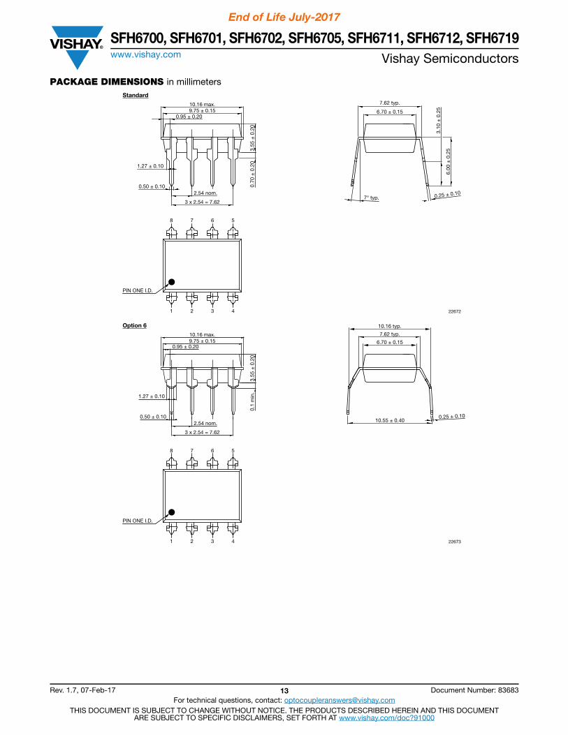
PACKAGE DIMENSIONS in millimeters
22672
10.16 max.9.75 ± 0.15
1.27 ± 0.10
0.50 ± 0.102.54 nom.
3 x 2.54 = 7.62
3.55
± 0
.20
0.70
± 0
.20
0.95 ± 0.20
7.62 typ.
6.70 ± 0.15
7° typ. 0.25 ± 0.10
3.10
± 0
.25
6.00
± 0
.25
Standard
PIN ONE I.D.
8 7 6 5
21 43
PIN ONE I.D.
8 7 6 5
21 43
10.16 max.9.75 ± 0.15
1.27 ± 0.10
0.50 ± 0.102.54 nom.
3 x 2.54 = 7.62
3.55
± 0
.20
0.1
min
.
0.95 ± 0.20
10.16 typ.
7.62 typ.
6.70 ± 0.15
10.55 ± 0.400.25 ± 0.10
22673
Option 6
SFH6700, SFH6701, SFH6702, SFH6705, SFH6711, SFH6712, SFH6719www.vishay.com Vishay Semiconductors
End of Life July-2017
Rev. 1.7, 07-Feb-17 14 Document Number: 83683For technical questions, contact: [email protected]
THIS DOCUMENT IS SUBJECT TO CHANGE WITHOUT NOTICE. THE PRODUCTS DESCRIBED HEREIN AND THIS DOCUMENTARE SUBJECT TO SPECIFIC DISCLAIMERS, SET FORTH AT www.vishay.com/doc?91000
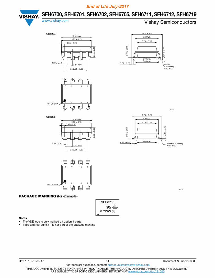
PACKAGE MARKING (for example)
Notes• The VDE logo is only marked on option 1 parts• Tape and reel suffix (T) is not part of the package marking
22674
Option 7
PIN ONE I.D.1 2 3 4
78 6 5
10.16 max.
9.75 ± 0.15
1.27 ± 0.102.54 nom.
3 x 2.54 = 7.62
3.55
± 0
.20
0.95 ± 0.20
LeadsCoplanarity0.10 max.
0.25
± 0
.10
10.05 ± 0.25
7.62 typ.
8.00 min.
6.70 ± 0.15
0.70
± 0
.20
0.75 ± 0.258.40 min.
22675
Option 9
PIN ONE I.D.1 2 3 4
78 6 5
10.16 max.9.75 ± 0.15
1.27 ± 0.102.54 nom.
3 x 2.54 = 7.62
3.55
± 0
.20
0.95 ± 0.20
Leads Coplanarity0.10 max.
7.62 typ.
8.00 min.
6.70 ± 0.15
0.25
± 0
.10
0.75 ± 0.20
9.78 ± 0.25
0.18
± 0
.08
SFH6700
V YWW 68
Footprint and Schematic Informationwww.vishay.com Vishay Semiconductors
Rev. 1.0, 08-May-17 1 Document Number: 84498For technical questions, contact: [email protected]
THIS DOCUMENT IS SUBJECT TO CHANGE WITHOUT NOTICE. THE PRODUCTS DESCRIBED HEREIN AND THIS DOCUMENTARE SUBJECT TO SPECIFIC DISCLAIMERS, SET FORTH AT www.vishay.com/doc?91000
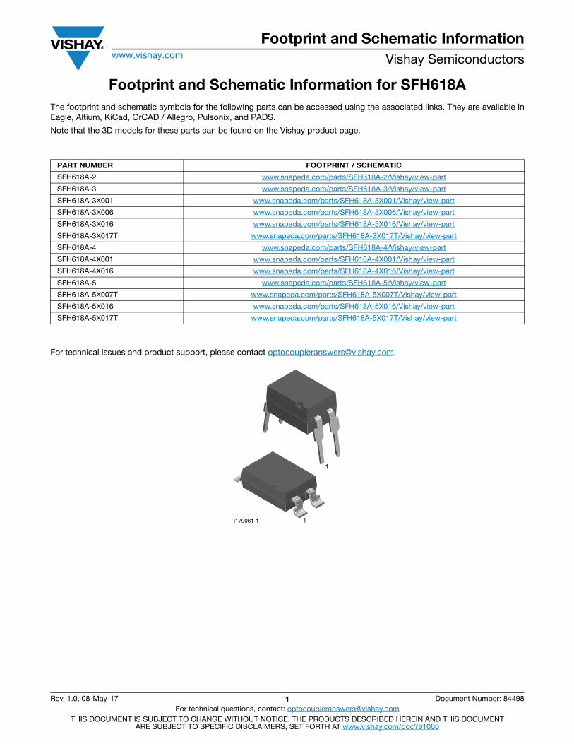
Footprint and Schematic Information for SFH618AThe footprint and schematic symbols for the following parts can be accessed using the associated links. They are available in Eagle, Altium, KiCad, OrCAD / Allegro, Pulsonix, and PADS.
Note that the 3D models for these parts can be found on the Vishay product page.
For technical issues and product support, please contact [email protected].
PART NUMBER FOOTPRINT / SCHEMATIC
SFH618A-2 www.snapeda.com/parts/SFH618A-2/Vishay/view-part
SFH618A-3 www.snapeda.com/parts/SFH618A-3/Vishay/view-part
SFH618A-3X001 www.snapeda.com/parts/SFH618A-3X001/Vishay/view-part
SFH618A-3X006 www.snapeda.com/parts/SFH618A-3X006/Vishay/view-part
SFH618A-3X016 www.snapeda.com/parts/SFH618A-3X016/Vishay/view-part
SFH618A-3X017T www.snapeda.com/parts/SFH618A-3X017T/Vishay/view-part
SFH618A-4 www.snapeda.com/parts/SFH618A-4/Vishay/view-part
SFH618A-4X001 www.snapeda.com/parts/SFH618A-4X001/Vishay/view-part
SFH618A-4X016 www.snapeda.com/parts/SFH618A-4X016/Vishay/view-part
SFH618A-5 www.snapeda.com/parts/SFH618A-5/Vishay/view-part
SFH618A-5X007T www.snapeda.com/parts/SFH618A-5X007T/Vishay/view-part
SFH618A-5X016 www.snapeda.com/parts/SFH618A-5X016/Vishay/view-part
SFH618A-5X017T www.snapeda.com/parts/SFH618A-5X017T/Vishay/view-part
1
1
i179061-1
Legal Disclaimer Noticewww.vishay.com Vishay
Revision: 08-Feb-17 1 Document Number: 91000
DisclaimerALL PRODUCT, PRODUCT SPECIFICATIONS AND DATA ARE SUBJECT TO CHANGE WITHOUT NOTICE TO IMPROVE RELIABILITY, FUNCTION OR DESIGN OR OTHERWISE.
Vishay Intertechnology, Inc., its affiliates, agents, and employees, and all persons acting on its or their behalf (collectively, “Vishay”), disclaim any and all liability for any errors, inaccuracies or incompleteness contained in any datasheet or in any other disclosure relating to any product.
Vishay makes no warranty, representation or guarantee regarding the suitability of the products for any particular purpose or the continuing production of any product. To the maximum extent permitted by applicable law, Vishay disclaims (i) any and all liability arising out of the application or use of any product, (ii) any and all liability, including without limitation special, consequential or incidental damages, and (iii) any and all implied warranties, including warranties of fitness for particular purpose, non-infringement and merchantability.
Statements regarding the suitability of products for certain types of applications are based on Vishay’s knowledge of typical requirements that are often placed on Vishay products in generic applications. Such statements are not binding statements about the suitability of products for a particular application. It is the customer’s responsibility to validate that a particular product with the properties described in the product specification is suitable for use in a particular application. Parameters provided in datasheets and / or specifications may vary in different applications and performance may vary over time. All operating parameters, including typical parameters, must be validated for each customer application by the customer’s technical experts. Product specifications do not expand or otherwise modify Vishay’s terms and conditions of purchase, including but not limited to the warranty expressed therein.
Except as expressly indicated in writing, Vishay products are not designed for use in medical, life-saving, or life-sustaining applications or for any other application in which the failure of the Vishay product could result in personal injury or death. Customers using or selling Vishay products not expressly indicated for use in such applications do so at their own risk. Please contact authorized Vishay personnel to obtain written terms and conditions regarding products designed for such applications.
No license, express or implied, by estoppel or otherwise, to any intellectual property rights is granted by this document or by any conduct of Vishay. Product names and markings noted herein may be trademarks of their respective owners.
© 2017 VISHAY INTERTECHNOLOGY, INC. ALL RIGHTS RESERVED
![Product Specifications - · PDF fileProduct Specifications Physical Characteristics ... the conditions specified in CENELEC standard EN 45502-2-1:2003, ... (124 μs + [4 μs x Rload])](https://static.fdocument.org/doc/165x107/5ab6de537f8b9a86428e2035/product-specifications-product-specifications-physical-characteristics-the.jpg)