EVALUATION KIT AVAILABLE Dual and Combinable … MAX17008.pdf · 1.3mV/μs for SMPS1 at CSL1 and...
36
General Description The MAX17007A/MAX17008 are dual Quick-PWM™ step-down controllers intended for general power gen- eration in battery-powered systems. The two switched- mode power supplies (SMPSs) can also be combined to operate in a two-phase single-output mode. Constant on-time Quick-PWM operation provides fast response to load transients and handles wide input/output (I/O) volt- age ratios with ease, while maintaining a relatively con- stant switching frequency. The switching frequency can be individually adjusted between 200kHz and 600kHz with external resistors. Differential output current sens- ing allows output sense-resistor sensing for an accurate current limit, or lossless inductor direct-current resis- tance (DCR) current sensing for lower power dissipation while maintaining 0.7% output accuracy. Overvoltage (MAX17007A only), undervoltage protection, and accu- rate user-selectable current limits (15mV, 30mV, 45mV, and 60mV) ensure robust operations. The SMPS outputs can operate in skip mode or in ultra- sonic mode for improved light-load efficiency. The ultra- sonic mode eliminates audible noises by maintaining a minimum switching frequency of 25kHz in pulse- skipping mode. The output voltage of SMPS1 can be dynamically adjusted by changing the voltage at the REFIN1 pin. The device includes a 0.5% accurate reference output that can be used to set the REFIN1 voltage. An external 5V bias supply is required to power the internal circuitry and its gate drivers. Independent on/off controls with well-defined logic thresh- olds and independent open-drain power-good outputs provide flexible system configurations. To prevent current surges at startup, the internal voltage target is slowly ramped up from zero to the final target with a slew rate of 1.3mV/μs for SMPS1 at CSL1 and 0.65mV/μs for SMPS2 at FB2. To prevent the output from ringing off below ground in shutdown, the internal voltage target is ramped down from its previous value to zero with the same respective slew rates. Integrated bootstrap switches eliminate the need for external bootstrap diodes. The MAX17007A/MAX17008 are available in a space- saving, 28-pin, 4mm x 4mm, thin QFN package with an exposed backside pad. Applications Features ♦ Dual Quick-PWM with Fast Transient Response ♦ Automatic Dynamic REFIN1 Detection and PGOOD1/Fault Blanking ♦ Fixed and Adjustable Output Voltages ±0.7% Output Accuracy Over Line and Load OUT1: 0 to 2V Dynamic Output or Preset 1.05V OUT2: 0.7V to 2V Range or Preset 1.5V ♦ Resistor-Programmable Switching Frequency ♦ Integrated BST Switches ♦ Differential Current-Sense Inputs Low-Cost DCR Sensing or Accurate Current- Sense Resistors Internally Coupled Current-Sense Compensation ♦ Combinable Mode Supports High-Current Dynamic Output Voltages ♦ Selectable Forced-PWM, Pulse Skip, or Ultrasonic Mode Operation ♦ 26V Maximum Input Voltage Rating ♦ Independent Enable Inputs ♦ Independent Power-Good Outputs ♦ Overvoltage Protection (MAX17007A Only) ♦ Undervoltage/Thermal Protection ♦ Voltage Soft-Start and Soft-Shutdown MAX17007A/MAX17008 Dual and Combinable QPWM Graphics Core Controllers for Notebook Computers ________________________________________________________________ Maxim Integrated Products 1 MAX17007A MAX17008 18 THIN QFN (4mm x 4mm) 4 17 5 16 6 15 14 22 7 19 3 20 2 21 13 23 12 24 11 25 10 26 9 27 8 28 1 LX1 DH1 PGOOD1 EN1 CSH1 TOP VIEW *EP *EP = EXPOSED PAD. CSL1 REFIN1 LX2 DH2 PGOOD2 EN2 CSH2 CSL2 FB2 BST2 PGND DL2 V DD DL1 GND BST1 REF ILIM1 (CCI) ILIM2 V CC SKIP TON1 TON2 + Pin Configuration Ordering Information 19-3200; Rev 2; 10/08 For pricing, delivery, and ordering information, please contact Maxim Direct at 1-888-629-4642, or visit Maxim’s website at www.maxim-ic.com. EVALUATION KIT AVAILABLE +Denotes a lead-free/RoHS-compliant package. *EP = Exposed pad. PART TEMP RANGE PIN-PACKAGE MAX17007AGTI+ -40°C to +105°C 28 Thin QFN-EP* MAX17008GTI+ -40°C to +105°C 28 Thin QFN-EP* Notebook Computers Low-Power I/O Supplies GPU Core Supplies 2 to 4 Li+ Cells Battery- Powered Devices Quick-PWM is a trademark of Maxim Integrated Products, Inc.
Transcript of EVALUATION KIT AVAILABLE Dual and Combinable … MAX17008.pdf · 1.3mV/μs for SMPS1 at CSL1 and...
General DescriptionThe MAX17007A/MAX17008 are dual Quick-PWM™step-down controllers intended for general power gen-eration in battery-powered systems. The two switched-mode power supplies (SMPSs) can also be combined tooperate in a two-phase single-output mode. Constanton-time Quick-PWM operation provides fast response toload transients and handles wide input/output (I/O) volt-age ratios with ease, while maintaining a relatively con-stant switching frequency. The switching frequency canbe individually adjusted between 200kHz and 600kHzwith external resistors. Differential output current sens-ing allows output sense-resistor sensing for an accuratecurrent limit, or lossless inductor direct-current resis-tance (DCR) current sensing for lower power dissipationwhile maintaining 0.7% output accuracy. Overvoltage(MAX17007A only), undervoltage protection, and accu-rate user-selectable current limits (15mV, 30mV, 45mV,and 60mV) ensure robust operations.
The SMPS outputs can operate in skip mode or in ultra-sonic mode for improved light-load efficiency. The ultra-sonic mode eliminates audible noises by maintaining aminimum switching frequency of 25kHz in pulse-skipping mode.
The output voltage of SMPS1 can be dynamicallyadjusted by changing the voltage at the REFIN1 pin.The device includes a 0.5% accurate reference outputthat can be used to set the REFIN1 voltage. An external5V bias supply is required to power the internal circuitryand its gate drivers.
Independent on/off controls with well-defined logic thresh-olds and independent open-drain power-good outputsprovide flexible system configurations. To prevent currentsurges at startup, the internal voltage target is slowlyramped up from zero to the final target with a slew rate of1.3mV/μs for SMPS1 at CSL1 and 0.65mV/μs for SMPS2at FB2. To prevent the output from ringing off belowground in shutdown, the internal voltage target is rampeddown from its previous value to zero with the samerespective slew rates. Integrated bootstrap switcheseliminate the need for external bootstrap diodes.
The MAX17007A/MAX17008 are available in a space-saving, 28-pin, 4mm x 4mm, thin QFN package with anexposed backside pad.
Applications
Features� Dual Quick-PWM with Fast Transient Response� Automatic Dynamic REFIN1 Detection and
PGOOD1/Fault Blanking� Fixed and Adjustable Output Voltages
±0.7% Output Accuracy Over Line and LoadOUT1: 0 to 2V Dynamic Output or Preset 1.05VOUT2: 0.7V to 2V Range or Preset 1.5V
� Resistor-Programmable Switching Frequency� Integrated BST Switches� Differential Current-Sense Inputs
Low-Cost DCR Sensing or Accurate Current-Sense ResistorsInternally Coupled Current-Sense Compensation
� Combinable Mode Supports High-CurrentDynamic Output Voltages
� Selectable Forced-PWM, Pulse Skip, or UltrasonicMode Operation
� 26V Maximum Input Voltage Rating� Independent Enable Inputs� Independent Power-Good Outputs� Overvoltage Protection (MAX17007A Only)� Undervoltage/Thermal Protection� Voltage Soft-Start and Soft-Shutdown
MA
X1
70
07
A/M
AX
17
00
8
Dual and Combinable QPWM GraphicsCore Controllers for Notebook Computers
________________________________________________________________ Maxim Integrated Products 1
MAX17007AMAX17008
18
THIN QFN(4mm x 4mm)
4
17
5
16
6
15
1422
7
19
3
20
2
21
1323
1224
1125
1026
927
828
1
LX1
DH1
PGOOD1
EN1
CSH1
TOP VIEW
*EP
*EP = EXPOSED PAD.
CSL1
REFIN1
LX2
DH2
PGOOD2
EN2
CSH2
CSL2
FB2
BST2
PGND
DL2
V DD
DL1
GND
BST1
REF
ILIM
1
(CCI
) ILI
M2
V CC
SKIP
TON1
TON2
+
Pin Configuration
Ordering Information
19-3200; Rev 2; 10/08
For pricing, delivery, and ordering information, please contact Maxim Direct at 1-888-629-4642,or visit Maxim’s website at www.maxim-ic.com.
EVALUATION KIT
AVAILABLE
+Denotes a lead-free/RoHS-compliant package.*EP = Exposed pad.
PART TEMP RANGE PIN-PACKAGE
MAX17007AGTI+ -40°C to +105°C 28 Thin QFN-EP*
MAX17008GTI+ -40°C to +105°C 28 Thin QFN-EP*
Notebook Computers
Low-Power I/O Supplies
GPU Core Supplies
2 to 4 Li+ Cells Battery-Powered Devices
Quick-PWM is a trademark of Maxim Integrated Products, Inc.
MA
X1
70
07
A/M
AX
17
00
8
Dual and Combinable QPWM GraphicsCore Controllers for Notebook Computers
2 _______________________________________________________________________________________
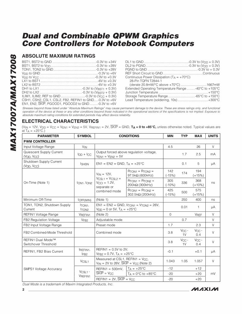
ABSOLUTE MAXIMUM RATINGS
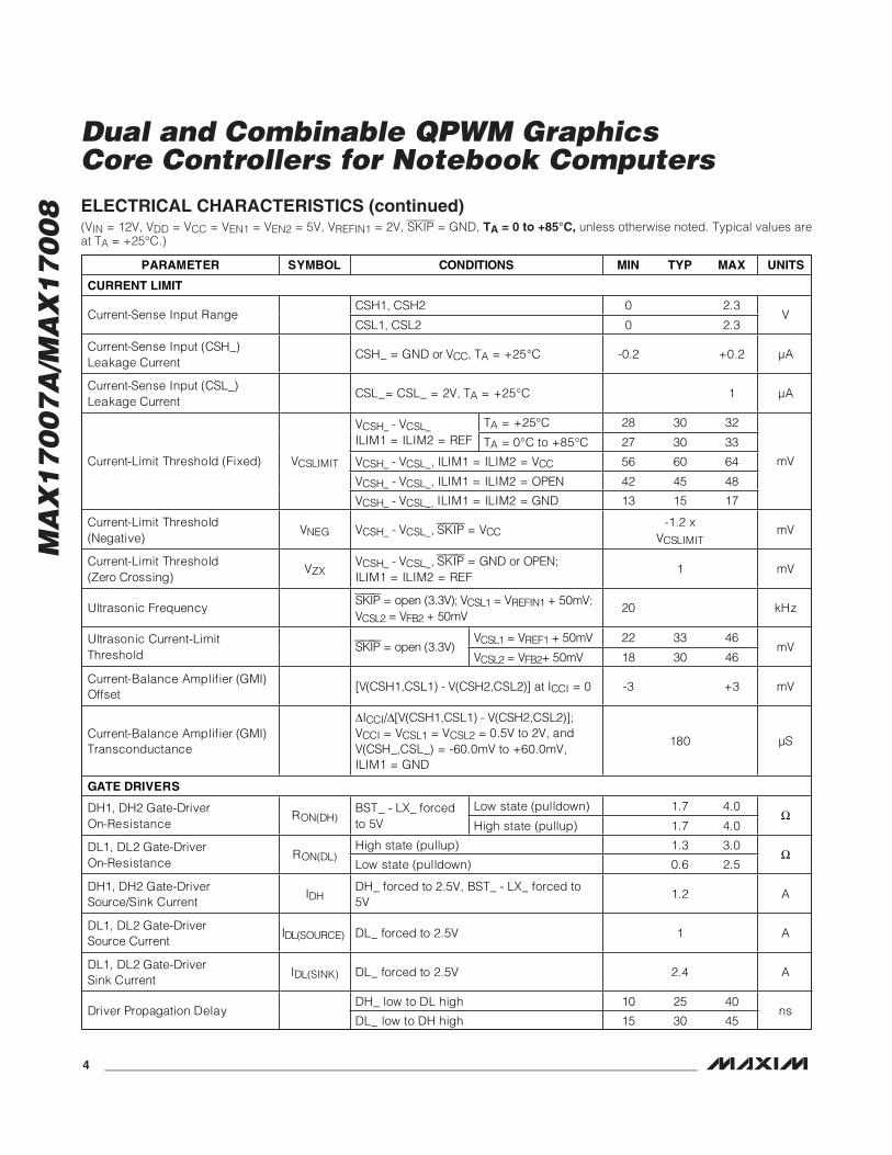
ELECTRICAL CHARACTERISTICS(VIN = 12V, VDD = VCC = VEN1 = VEN2 = 5V, VREFIN1 = 2V, SKIP = GND, TA = 0 to +85°C, unless otherwise noted. Typical values areat TA = +25°C.)
Stresses beyond those listed under “Absolute Maximum Ratings” may cause permanent damage to the device. These are stress ratings only, and functionaloperation of the device at these or any other conditions beyond those indicated in the operational sections of the specifications is not implied. Exposure toabsolute maximum rating conditions for extended periods may affect device reliability.
BST1, BST2 to GND ...............................................-0.3V to +34VBST1, BST2 to VDD.................................................-0.3V to +28VTON1, TON2 to GND..............................................-0.3V to +28VVDD to GND..............................................................-0.3V to +6VVDD to VCC ............................................................-0.3V to +0.3VLX1 to BST1..............................................................-6V to +0.3VLX2 to BST2..............................................................-6V to +0.3VDH1 to LX1 ..............................................-0.3V to (VBST1 + 0.3V)DH2 to LX2 ..............................................-0.3V to (VBST2 + 0.3V)ILIM1, ILIM2, REF to GND ..........................-0.3V to (VCC + 0.3V)CSH1, CSH2, CSL1, CSL2, FB2, REFIN1 to GND....-0.3V to +6VEN1, EN2, SKIP, PGOOD1, PGOOD2 to GND.........-0.3V to +6V
DL1 to GND ................................................-0.3V to (VDD + 0.3V)DL2 to PGND..............................................-0.3V to (VDD + 0.3V)PGND to GND ......................................................-0.3V to + 0.3VREF Short Circuit to GND...........................................ContinuousContinuous Power Dissipation (TA = +70°C)
28-Pin TQFN T2844-1(derate 20.8mW/°C above +70°C) ............................1667mW
Extended Operating Temperature Range .........-40°C to +105°CJunction Temperature ......................................................+150°CStorage Temperature Range .............................-65°C to +150°CLead Temperature (soldering, 10s) .................................+300°C
PARAMETER SYMBOL CONDITIONS MIN TYP MAX UNITS
PWM CONTROLLER
Input Voltage Range VIN 4.5 26 V
Quiescent Supply Current (VDD, VCC)
IDD + ICCOutput forced above regulation voltage, VEN1 = VEN2 = 5V
1.7 2.5 mA
Shutdown Supply Current (VDD, VCC)
ISHDN EN1 = EN2 = GND, TA = +25°C 0.1 5 μA
RTON1 = RTON2 = 97.5k (600kHz)
142 (-15%)
174 194
(+15%)
RTON1 = RTON2 =200k (300kHz)
305 (-10%)
336 368
(+10%) On-Time (Note 1) tON1, tON2
VIN = 12V, VCSL1 = VCSL2 =VCCI = 1.2V, separate or combined mode RTON1 = RTON2 =
302.5k (200kHz) 425
(-15%) 500
575 (+15%)
ns
Minimum Off-Time tOFF(MIN) (Note 1) 250 400 ns
TON1, TON2, Shutdown Supply Current
ITON1,ITON2
EN1 = EN2 = GND, VTON1 = VTON2 = 26V, VDD = 0 or 5V, TA = +25°C
0.01 1 μA
REFIN1 Voltage Range VREFIN1 (Note 2) 0 VREF V
FB2 Regulation Voltage VFB2 Adjustable mode 0.7 V
FB2 Input Voltage Range Preset mode 1.7 2.3 V
FB2 Combined-Mode Threshold Combined mode 3.8 VCC -
1V VCC - 0.4
V
REFIN1 Dual Mode™ Switchover Threshold
3.8 VCC -
1V VCC - 0.4
V
REFIN1, FB2 Bias Current IREFIN1,
IFB2
REFIN1 = 0.5V to 2V; VFB2 = 0.7V, TA = +25°C
-0.1 +0.1 μA
VCSL1 Measured at CSL1, REFIN1 = VCC,VIN = 2V to 26V, SKIP = VCC (Note 2)
1.043 1.05 1.057 V
TA = +25°C -12 +12 REFIN1 = 500mV, SKIP = VCC TA = 0°C to +85°C -20 +20
SMPS1 Voltage Accuracy VCSL1 - VREFIN1
REFIN1 = 2V, SKIP = VCC -20 +20
mV
Dual Mode is a trademark of Maxim Integrated Products, Inc.
MA
X1
70
07
A/M
AX
17
00
8
Dual and Combinable QPWM GraphicsCore Controllers for Notebook Computers
_______________________________________________________________________________________ 3
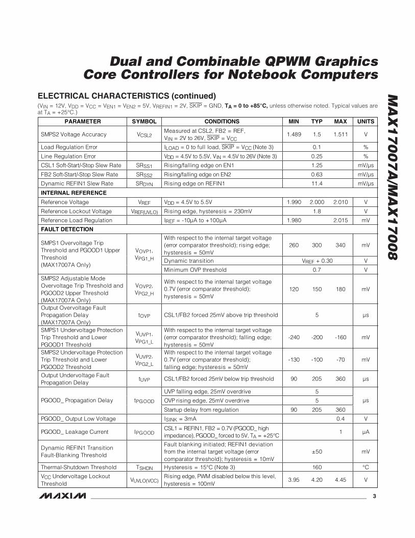
PARAMETER SYMBOL CONDITIONS MIN TYP MAX UNITS
SMPS2 Voltage Accuracy VCSL2 Measured at CSL2, FB2 = REF, VIN = 2V to 26V, SKIP = VCC
1.489 1.5 1.511 V
Load Regulation Error ILOAD = 0 to full load, SKIP = VCC (Note 3) 0.1 %
Line Regulation Error VDD = 4.5V to 5.5V, VIN = 4.5V to 26V (Note 3) 0.25 %
CSL1 Soft-Start/-Stop Slew Rate SRSS1 Rising/falling edge on EN1 1.25 mV/μs
FB2 Soft-Start/-Stop Slew Rate SRSS2 Rising/falling edge on EN2 0.63 mV/μs
Dynamic REFIN1 Slew Rate SRDYN Rising edge on REFIN1 11.4 mV/μs
INTERNAL REFERENCE
Reference Voltage VREF VDD = 4.5V to 5.5V 1.990 2.000 2.010 V
Reference Lockout Voltage VREF(UVLO) Rising edge, hysteresis = 230mV 1.8 V
Reference Load Regulation IREF = -10μA to +100μA 1.980 2.015 mV
FAULT DETECTION
With respect to the internal target voltage (error comparator threshold); rising edge; hysteresis = 50mV
260 300 340 mV
Dynamic transition VREF + 0.30 V
SMPS1 Overvoltage Trip Threshold and PGOOD1 Upper Threshold (MAX17007A Only)
VOVP1,VPG1_H
Minimum OVP threshold 0.7 V
SMPS2 Adjustable Mode Overvoltage Trip Threshold and PGOOD2 Upper Threshold (MAX17007A Only)
VOVP2,VPG2_H
With respect to the internal target voltage 0.7V (error comparator threshold); hysteresis = 50mV
120 150 180 mV
Output Overvoltage Fault Propagation Delay (MAX17007A Only)
tOVP CSL1/FB2 forced 25mV above trip threshold 5 μs
SMPS1 Undervoltage Protection Trip Threshold and Lower PGOOD1 Threshold
VUVP1,VPG1_L
With respect to the internal target voltage (error comparator threshold); falling edge; hysteresis = 50mV
-240 -200 -160 mV
SMPS2 Undervoltage Protection Trip Threshold and Lower PGOOD2 Threshold
VUVP2,VPG2_L
With respect to the internal target voltage 0.7V (error comparator threshold); falling edge; hysteresis = 50mV
-130 -100 -70 mV
Output Undervoltage Fault Propagation Delay
tUVP CSL1/FB2 forced 25mV below trip threshold 90 205 360 μs
UVP falling edge, 25mV overdrive 5
OVP rising edge, 25mV overdrive 5 PGOOD_ Propagation Delay tPGOOD
Startup delay from regulation 90 205 360
μs
PGOOD_ Output Low Voltage ISINK = 3mA 0.4 V
PGOOD_ Leakage Current IPGOOD CSL1 = REFIN1, FB2 = 0.7V (PGOOD_ high impedance), PGOOD_ forced to 5V, TA = +25°C
1 μA
Dynamic REFIN1 Transition Fault-Blanking Threshold
Fault blanking initiated; REFIN1 deviation from the internal target voltage (error comparator threshold); hysteresis = 10mV
±50 mV
Thermal-Shutdown Threshold TSHDN Hysteresis = 15°C (Note 3) 160 °C
VCC Undervoltage Lockout Threshold
VUVLO(VCC) Rising edge, PWM disabled below this level, hysteresis = 100mV
3.95 4.20 4.45 V
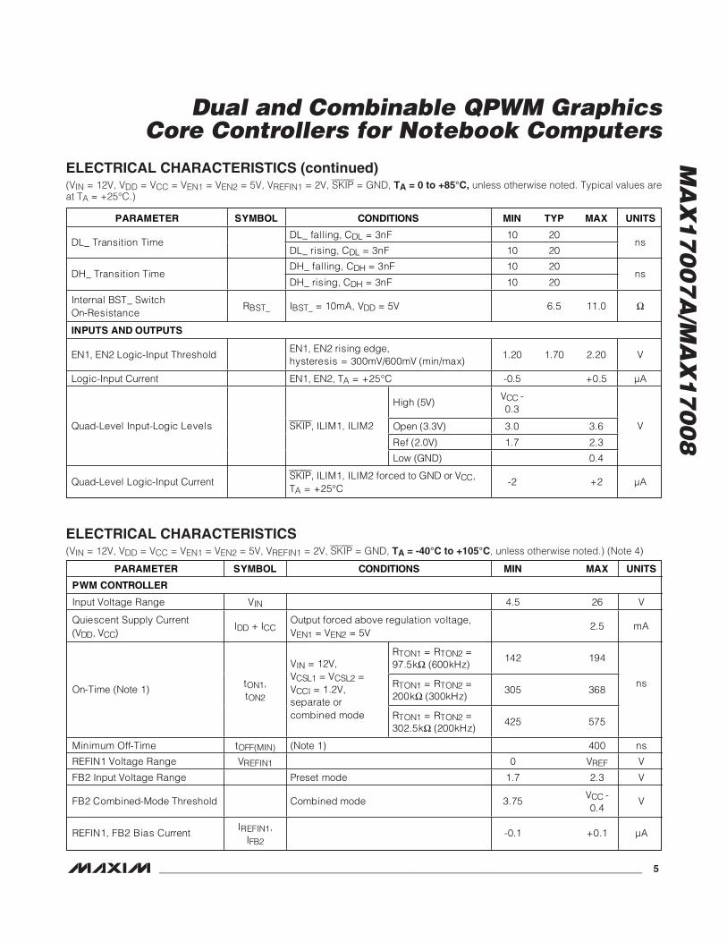
ELECTRICAL CHARACTERISTICS (continued)(VIN = 12V, VDD = VCC = VEN1 = VEN2 = 5V, VREFIN1 = 2V, SKIP = GND, TA = 0 to +85°C, unless otherwise noted. Typical values areat TA = +25°C.)
MA
X1
70
07
A/M
AX
17
00
8
Dual and Combinable QPWM GraphicsCore Controllers for Notebook Computers
4 _______________________________________________________________________________________
ELECTRICAL CHARACTERISTICS (continued)(VIN = 12V, VDD = VCC = VEN1 = VEN2 = 5V, VREFIN1 = 2V, SKIP = GND, TA = 0 to +85°C, unless otherwise noted. Typical values areat TA = +25°C.)
PARAMETER SYMBOL CONDITIONS MIN TYP MAX UNITS
CURRENT LIMIT
CSH1, CSH2 0 2.3 Current-Sense Input Range
CSL1, CSL2 0 2.3 V
Current-Sense Input (CSH_) Leakage Current
CSH_ = GND or VCC, TA = +25°C -0.2 +0.2 μA
Current-Sense Input (CSL_) Leakage Current
CSL_= CSL_ = 2V, TA = +25°C 1 μA
TA = +25°C 28 30 32 VCSH_ - VCSL_ ILIM1 = ILIM2 = REF TA = 0°C to +85°C 27 30 33
VCSH_ - VCSL_, ILIM1 = ILIM2 = VCC 56 60 64
VCSH_ - VCSL_, ILIM1 = ILIM2 = OPEN 42 45 48
Current-Limit Threshold (Fixed) VCSLIMIT
VCSH_ - VCSL_, ILIM1 = ILIM2 = GND 13 15 17
mV
Current-Limit Threshold (Negative)
VNEG VCSH_ - VCSL_, SKIP = VCC-1.2 x
VCSLIMIT mV
Current-Limit Threshold (Zero Crossing)
VZX VCSH_ - VCSL_, SKIP = GND or OPEN; ILIM1 = ILIM2 = REF
1 mV
Ultrasonic Frequency SKIP = open (3.3V); VCSL1 = VREFIN1 + 50mV; VCSL2 = VFB2 + 50mV
20 kHz
VCSL1 = VREF1 + 50mV 22 33 46 Ultrasonic Current-Limit Threshold
SKIP = open (3.3V) VCSL2 = VFB2+ 50mV 18 30 46
mV
Current-Balance Amplifier (GMI) Offset
[V(CSH1,CSL1) - V(CSH2,CSL2)] at ICCI = 0 -3 +3 mV
Current-Balance Amplifier (GMI) Transconductance
ICCI/ [V(CSH1,CSL1) - V(CSH2,CSL2)]; VCCI = VCSL1 = VCSL2 = 0.5V to 2V, and V(CSH_,CSL_) = -60.0mV to +60.0mV, ILIM1 = GND
180 μS
GATE DRIVERS
Low state (pulldown) 1.7 4.0 DH1, DH2 Gate-Driver On-Resistance
RON(DH) BST_ - LX_ forced to 5V High state (pullup) 1.7 4.0
High state (pullup) 1.3 3.0 DL1, DL2 Gate-Driver On-Resistance
RON(DL) Low state (pulldown) 0.6 2.5
DH1, DH2 Gate-Driver Source/Sink Current
IDH DH_ forced to 2.5V, BST_ - LX_ forced to 5V
1.2 A
DL1, DL2 Gate-Driver Source Current
IDL(SOURCE) DL_ forced to 2.5V 1 A
DL1, DL2 Gate-Driver Sink Current
IDL(SINK) DL_ forced to 2.5V 2.4 A
DH_ low to DL high 10 25 40 Driver Propagation Delay
DL_ low to DH high 15 30 45 ns
MA
X1
70
07
A/M
AX
17
00
8
Dual and Combinable QPWM GraphicsCore Controllers for Notebook Computers
_______________________________________________________________________________________ 5
ELECTRICAL CHARACTERISTICS (continued)(VIN = 12V, VDD = VCC = VEN1 = VEN2 = 5V, VREFIN1 = 2V, SKIP = GND, TA = 0 to +85°C, unless otherwise noted. Typical values areat TA = +25°C.)
PARAMETER SYMBOL CONDITIONS MIN TYP MAX UNITS
DL_ falling, CDL = 3nF 10 20 DL_ Transition Time
DL_ rising, CDL = 3nF 10 20 ns
DH_ falling, CDH = 3nF 10 20 DH_ Transition Time
DH_ rising, CDH = 3nF 10 20 ns
Internal BST_ Switch On-Resistance
RBST_ IBST_ = 10mA, VDD = 5V 6.5 11.0
INPUTS AND OUTPUTS
EN1, EN2 Logic-Input Threshold EN1, EN2 rising edge, hysteresis = 300mV/600mV (min/max)
1.20 1.70 2.20 V
Logic-Input Current EN1, EN2, TA = +25°C -0.5 +0.5 μA
High (5V) VCC - 0.3
Open (3.3V) 3.0 3.6
Ref (2.0V) 1.7 2.3
Quad-Level Input-Logic Levels SKIP, ILIM1, ILIM2
Low (GND) 0.4
V
Quad-Level Logic-Input Current SKIP, ILIM1, ILIM2 forced to GND or VCC,TA = +25°C
-2 +2 μA
ELECTRICAL CHARACTERISTICS(VIN = 12V, VDD = VCC = VEN1 = VEN2 = 5V, VREFIN1 = 2V, SKIP = GND, TA = -40°C to +105°C, unless otherwise noted.) (Note 4)
PARAMETER SYMBOL CONDITIONS MIN MAX UNITS
PWM CONTROLLER
Input Voltage Range VIN 4.5 26 V
Quiescent Supply Current (VDD, VCC)
IDD + ICCOutput forced above regulation voltage, VEN1 = VEN2 = 5V
2.5 mA
RTON1 = RTON2 = 97.5k (600kHz)
142 194
RTON1 = RTON2 =200k (300kHz)
305 368 On-Time (Note 1) tON1,tON2
VIN = 12V, VCSL1 = VCSL2 =VCCI = 1.2V, separate or combined mode RTON1 = RTON2 =
302.5k (200kHz) 425 575
ns
Minimum Off-Time tOFF(MIN) (Note 1) 400 ns
REFIN1 Voltage Range VREFIN1 0 VREF V
FB2 Input Voltage Range Preset mode 1.7 2.3 V
FB2 Combined-Mode Threshold Combined mode 3.75 VCC - 0.4
V
REFIN1, FB2 Bias Current IREFIN1,
IFB2 -0.1 +0.1 μA
MA
X1
70
07
A/M
AX
17
00
8
Dual and Combinable QPWM GraphicsCore Controllers for Notebook Computers
6 _______________________________________________________________________________________
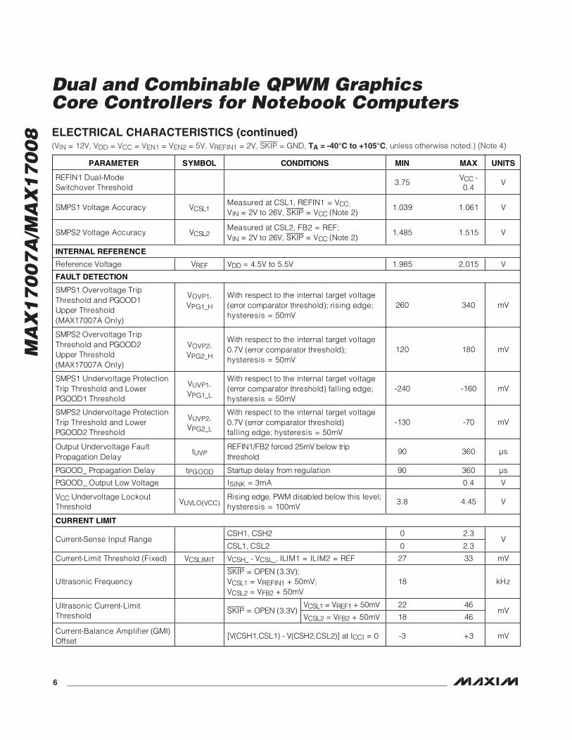
ELECTRICAL CHARACTERISTICS (continued)(VIN = 12V, VDD = VCC = VEN1 = VEN2 = 5V, VREFIN1 = 2V, SKIP = GND, TA = -40°C to +105°C, unless otherwise noted.) (Note 4)
PARAMETER SYMBOL CONDITIONS MIN MAX UNITS
REFIN1 Dual-Mode Switchover Threshold
3.75 VCC - 0.4
V
SMPS1 Voltage Accuracy VCSL1 Measured at CSL1, REFIN1 = VCC; VIN = 2V to 26V, SKIP = VCC (Note 2)
1.039 1.061 V
SMPS2 Voltage Accuracy VCSL2 Measured at CSL2, FB2 = REF; VIN = 2V to 26V, SKIP = VCC (Note 2)
1.485 1.515 V
INTERNAL REFERENCE
Reference Voltage VREF VDD = 4.5V to 5.5V 1.985 2.015 V
FAULT DETECTION
SMPS1 Overvoltage Trip Threshold and PGOOD1 Upper Threshold (MAX17007A Only)
VOVP1,VPG1_H
With respect to the internal target voltage (error comparator threshold); rising edge; hysteresis = 50mV
260 340 mV
SMPS2 Overvoltage Trip Threshold and PGOOD2 Upper Threshold (MAX17007A Only)
VOVP2,VPG2_H
With respect to the internal target voltage 0.7V (error comparator threshold); hysteresis = 50mV
120 180 mV
SMPS1 Undervoltage Protection Trip Threshold and Lower PGOOD1 Threshold
VUVP1,VPG1_L
With respect to the internal target voltage (error comparator threshold) falling edge; hysteresis = 50mV
-240 -160 mV
SMPS2 Undervoltage Protection Trip Threshold and Lower PGOOD2 Threshold
VUVP2,VPG2_L
With respect to the internal target voltage 0.7V (error comparator threshold) falling edge; hysteresis = 50mV
-130 -70 mV
Output Undervoltage Fault Propagation Delay
tUVP REFIN1/FB2 forced 25mV below trip threshold
90 360 μs
PGOOD_ Propagation Delay tPGOOD Startup delay from regulation 90 360 μs
PGOOD_ Output Low Voltage ISINK = 3mA 0.4 V
VCC Undervoltage Lockout Threshold
VUVLO(VCC) Rising edge, PWM disabled below this level; hysteresis = 100mV
3.8 4.45 V
CURRENT LIMIT
CSH1, CSH2 0 2.3 Current-Sense Input Range
CSL1, CSL2 0 2.3 V
Current-Limit Threshold (Fixed) VCSLIMIT VCSH_ - VCSL_, ILIM1 = ILIM2 = REF 27 33 mV
Ultrasonic Frequency SKIP = OPEN (3.3V); VCSL1 = VREFIN1 + 50mV; VCSL2 = VFB2 + 50mV
18 kHz
VCSL1 = VREF1 + 50mV 22 46 Ultrasonic Current-Limit Threshold
SKIP = OPEN (3.3V) VCSL2 = VFB2 + 50mV 18 46
mV
Current-Balance Amplifier (GMI) Offset
[V(CSH1,CSL1) - V(CSH2,CSL2)] at ICCI = 0 -3 +3 mV
MA
X1
70
07
A/M
AX
17
00
8
Dual and Combinable QPWM GraphicsCore Controllers for Notebook Computers
_______________________________________________________________________________________ 7
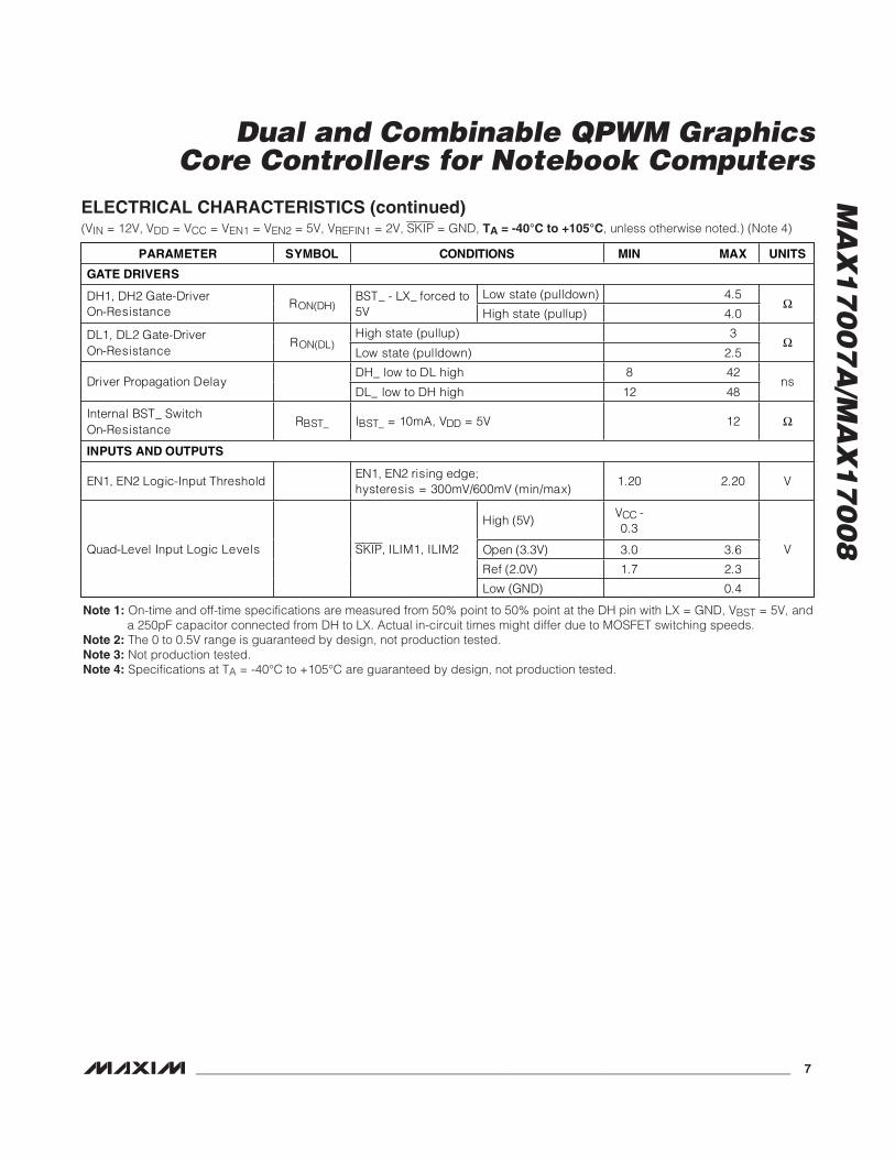
Note 1: On-time and off-time specifications are measured from 50% point to 50% point at the DH pin with LX = GND, VBST = 5V, anda 250pF capacitor connected from DH to LX. Actual in-circuit times might differ due to MOSFET switching speeds.
Note 2: The 0 to 0.5V range is guaranteed by design, not production tested.Note 3: Not production tested.Note 4: Specifications at TA = -40°C to +105°C are guaranteed by design, not production tested.
ELECTRICAL CHARACTERISTICS (continued)(VIN = 12V, VDD = VCC = VEN1 = VEN2 = 5V, VREFIN1 = 2V, SKIP = GND, TA = -40°C to +105°C, unless otherwise noted.) (Note 4)
PARAMETER SYMBOL CONDITIONS MIN MAX UNITS
GATE DRIVERS
Low state (pulldown) 4.5 DH1, DH2 Gate-Driver On-Resistance
RON(DH) BST_ - LX_ forced to 5V High state (pullup) 4.0
High state (pullup) 3 DL1, DL2 Gate-Driver On-Resistance
RON(DL) Low state (pulldown) 2.5
DH_ low to DL high 8 42 Driver Propagation Delay
DL_ low to DH high 12 48 ns
Internal BST_ Switch On-Resistance
RBST_ IBST_ = 10mA, VDD = 5V 12
INPUTS AND OUTPUTS
EN1, EN2 Logic-Input Threshold EN1, EN2 rising edge; hysteresis = 300mV/600mV (min/max)
1.20 2.20 V
High (5V) VCC - 0.3
Open (3.3V) 3.0 3.6
Ref (2.0V) 1.7 2.3
Quad-Level Input Logic Levels SKIP, ILIM1, ILIM2
Low (GND) 0.4
V
MA
X1
70
07
A/M
AX
17
00
8
Dual and Combinable QPWM GraphicsCore Controllers for Notebook Computers
8 _______________________________________________________________________________________
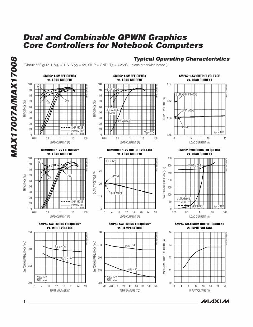
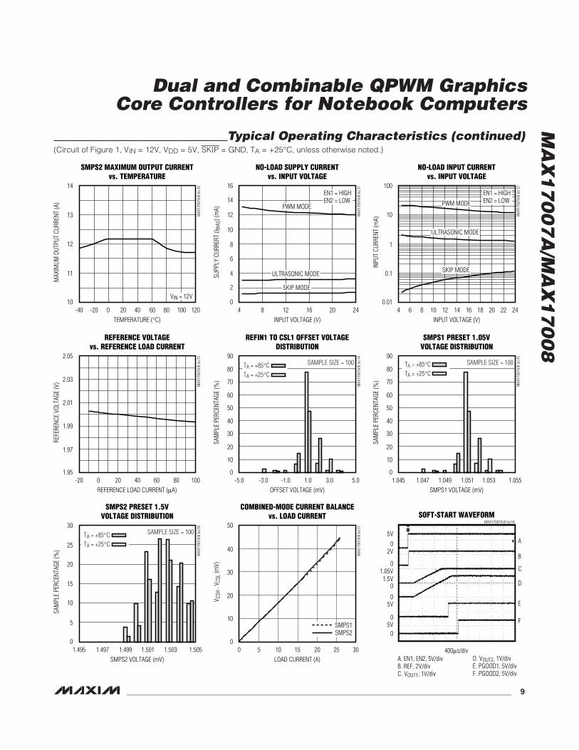
Typical Operating Characteristics(Circuit of Figure 1, VIN = 12V, VDD = 5V, SKIP = GND, TA = +25°C, unless otherwise noted.)
SMPS2 1.5V EFFICIENCYvs. LOAD CURRENT
MAX
1700
7A/8
toc0
1
LOAD CURRENT (A)
EFFI
CIEN
CY (%
)
1010.1
50
60
70
80
90
100
40
20
30
100.01 100
6V
12V20V
SKIP MODEPWM MODE
SMPS2 1.5V EFFICIENCYvs. LOAD CURRENT
MAX
1700
7A/8
toc0
2
LOAD CURRENT (A)
EFFI
CIEN
CY (%
)
1010.1
50
60
70
80
90
100
40
20
30
100.01 100
SKIP MODE
PWM MODE
VIN = 12V
ULTRASONICMODE
SMPS2 1.5V OUTPUT VOLTAGEvs. LOAD CURRENT
MAX
1700
7A/8
toc0
3
LOAD CURRENT (A)
OUTP
UT V
OLTA
GE (V
)
105
1.50
1.52
1.54
1.480 15
SKIP MODE
ULTRASONIC MODE
PWM
VIN = 12V
COMBINED 1.2V EFFICIENCYvs. LOAD CURRENT
MAX
1700
7A/8
toc0
4
LOAD CURRENT (A)
EFFI
CIEN
CY (%
)
1010.1
50
60
70
80
90
100
40
20
30
100.01 100
SKIP MODEPWM MODE
6V
12V 20V
COMBINED 1.2V OUTPUT VOLTAGEvs. LOAD CURRENT
MAX
1700
7A/8
toc0
5
LOAD CURRENT (A)
OUTP
UT V
OLTA
GE (V
)
16 2084 2412
1.19
1.20
1.21
1.22
1.180 28
SKIP MODE
PWM
VIN = 12V
SMPS2 SWITCHING FREQUENCYvs. LOAD CURRENT
MAX
1700
7A/8
toc0
6
LOAD CURRENT (A)
SWIT
CHIN
G FR
EQUE
NCY
(kHz
)
1010.1
200
250
300
350
150
50
100
00.01 100
SKIP MODE
PWM MODE
VIN = 12V
ULTRASONICMODE
SMPS2 SWITCHING FREQUENCYvs. INPUT VOLTAGE
MAX
1700
7A/8
toc0
7
INPUT VOLTAGE (V)
SWIT
CHIN
G FR
EQUE
NCY
(kHz
)
204 24
250
300
350
2000 288 12 16
VIN = 12VSKIP = 5V
IOUT2 = 5A
IOUT2 = 0A
SMPS2 SWITCHING FREQUENCYvs. TEMPERATURE
MAX
1700
7A/8
toc0
8
TEMPERATURE (°C)
SWIT
CHIN
G FR
EQUE
NCY
(kHz
)
0 40-20 60
290
270
310
330
250-40 1201008020
VIN = 12VSKIP = 5V
IOUT2 = 5A
IOUT2 = 0A
SMPS2 MAXIMUM OUTPUT CURRENTvs. INPUT VOLTAGE
MAX
1700
7A/8
toc0
9
INPUT VOLTAGE (V)
MAX
IMUM
OUT
PUT
CURR
ENT
(A)
204 24
12
11
13
14
100 288 12 16
MA
X1
70
07
A/M
AX
17
00
8
Dual and Combinable QPWM GraphicsCore Controllers for Notebook Computers
_______________________________________________________________________________________ 9
SMPS2 MAXIMUM OUTPUT CURRENTvs. TEMPERATURE
MAX
1700
7A/8
toc1
0
TEMPERATURE (°C)
MAX
IMUM
OUT
PUT
CURR
ENT
(A)
80400
11
12
13
14
10-40 1206020-20 100
VIN = 12V
NO-LOAD SUPPLY CURRENTvs. INPUT VOLTAGE
MAX
1700
7A/8
toc1
1
INPUT VOLTAGE (V)
SUPP
LY C
URRE
RT (I
BIAS
) (m
A)
2016
4
8
12
16
0
6
10
14
2
4 248 12
SKIP MODE
PWM MODE
ULTRASONIC MODE
EN1 = HIGHEN2 = LOW
NO-LOAD INPUT CURRENTvs. INPUT VOLTAGE
MAX
1700
7A/8
toc1
2
INPUT VOLTAGE (V)
INPU
T CU
RREN
T (m
A)
2016
0.1
1
10
100
0.014 248 12 1814 226 10
SKIP MODE
PWM MODE
ULTRASONIC MODE
EN1 = HIGHEN2 = LOW
REFERENCE VOLTAGEvs. REFERENCE LOAD CURRENT
MAX
1700
7A/8
toc1
3
REFERENCE LOAD CURRENT (μA)
REFE
RENC
E VO
LTAG
E (V
)
8060
1.99
1.97
2.01
2.03
2.05
1.95-20 10020 400
REFIN1 TO CSL1 OFFSET VOLTAGEDISTRIBUTION
MAX
1700
7A/8
toc1
4
OFFSET VOLTAGE (mV)
SAM
PLE
PERC
ENTA
GE (%
)
3.0
60
50
70
80
20
10
30
40
90
0-5.0 5.0-1.0 1.0-3.0
SAMPLE SIZE = 100TA = +85°CTA = +25°C
SMPS1 PRESET 1.05VVOLTAGE DISTRIBUTION
MAX
1700
7A/8
toc1
5
SMPS1 VOLTAGE (mV)
SAM
PLE
PERC
ENTA
GE (%
)
1.053
60
50
70
80
20
10
30
40
90
01.045 1.0551.049 1.0511.047
SAMPLE SIZE = 100TA = +85°CTA = +25°C
SMPS2 PRESET 1.5VVOLTAGE DISTRIBUTION
MAX
1700
7A/8
toc1
6
SMPS2 VOLTAGE (mV)
SAM
PLE
PERC
ENTA
GE (%
)
1.503
15
10
20
25
5
30
01.495 1.5051.499 1.5011.497
SAMPLE SIZE = 100TA = +85°CTA = +25°C
COMBINED-MODE CURRENT BALANCEvs. LOAD CURRENT
MAX
1700
7A/8
toc1
7
LOAD CURRENT (A)
V CSH
- V C
SL (m
V)
20155 2510
50
40
20
10
30
00 30
SMPS1SMPS2
SOFT-START WAVEFORMMAX17007A/8 toc18
400μs/div
A
B
E
F
C
D
5V
A. EN1, EN2, 5V/divB. REF, 2V/divC. VOUT1, 1V/div
D. VOUT2, 1V/divE. PGOOD1, 5V/divF. PGOOD2, 5V/div
02V
05V
0
05V
01.05V1.5V
0
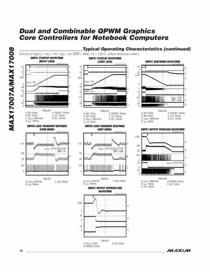
Typical Operating Characteristics (continued)(Circuit of Figure 1, VIN = 12V, VDD = 5V, SKIP = GND, TA = +25°C, unless otherwise noted.)
MA
X1
70
07
A/M
AX
17
00
8
Dual and Combinable QPWM GraphicsCore Controllers for Notebook Computers
10 ______________________________________________________________________________________
Typical Operating Characteristics (continued)(Circuit of Figure 1, VIN = 12V, VDD = 5V, SKIP = GND, TA = +25°C, unless otherwise noted.)
SMPS1 STARTUP WAVEFORM(HEAVY LOAD)
MAX17007A/8 toc19
200μs/div
A
B
E
F
G
C
D
5V
A. EN1, 5V/divB. REF, 2V/divC. VOUT1, 500mV/divD. ILX1, 10A/div
E. PGOOD1, 10V/divF. LX1, 10V/divG. DL1, 10V/div
02V
5V0
12V
05V
0
01.05V
08A
IOUT1 = 8A
SMPS1 STARTUP WAVEFORM(LIGHT LOAD)
MAX17007A/8 toc20
200μs/div
A
B
E
F
G
C
D
5V
A. EN1, 5V/divB. REF, 2V/divC. VOUT1, 500mV/divD. ILX1, 5A/div
SKIP = 5V
IOUT1 = 2A
E. PGOOD1, 10V/divF. LX1, 10V/divG. DL1, 10V/div
02V
01.05V
02A
05V
05V
0
012V
SMPS1 SHUTDOWN WAVEFORMMAX17007A/8 toc21
200μs/div
A
B
E
F
G
C
D
5V
A. EN1, 5V/divB. REF, 5V/divC. VOUT1, 500mV/divD. ILX1, 5A/div
E. PGOOD1, 10V/divF. LX1, 10V/divG. DL1, 10V/div
IOUT1 = 0.5ASKIP = GND
02V
1.05V
0
0
05V
0
5V0
12V
SMPS2 LOAD-TRANSIENT RESPONSE(PWM MODE)
MAX17007A/8 toc22
20μs/div
A
B
C
A. VOUT2, 50mV/divB. ILX2, 10A/div
C. LX2, 10V/div
1.5V
10A
2A
12V
0
IOUT2 = 2A TO 10A TO 2ASKIP = 5V
SMPS2 LOAD-TRANSIENT RESPONSE(SKIP MODE)
MAX17007A/8 toc23
20μs/div
A
B
C
A. VOUT2, 50mV/divB. ILX2, 10A/div
C. LX2, 10V/div
1.5V
8A
0A
12V
0
IOUT2 = 0.5A TO 8.5A TO 0.5ASKIP = GND
SMPS1 OUTPUT OVERLOAD WAVEFORMMAX17007A/8 toc24
200μs/div
A
B
E
C
DIOUT1 = 2A TO 15A
A. VOUT1, 500mV/divB. ILX1, 10A/divC. LX1, 10V/div
1.05V
10A
2A
5V
05V
12V
0
0
D. PGOOD1, 5V/divE. DL1, 5V/div
SMPS1 OUTPUT OVERVOLTAGEWAVEFORM
MAX17007A/8 toc25
40μs/div
A
B
C
A. VOUT1, 1V/divB. PGOOD1, 5V/div
C. DL1, 5V/div
1.05V
0
5V
0
5V
0
MA
X1
70
07
A/M
AX
17
00
8
Dual and Combinable QPWM GraphicsCore Controllers for Notebook Computers
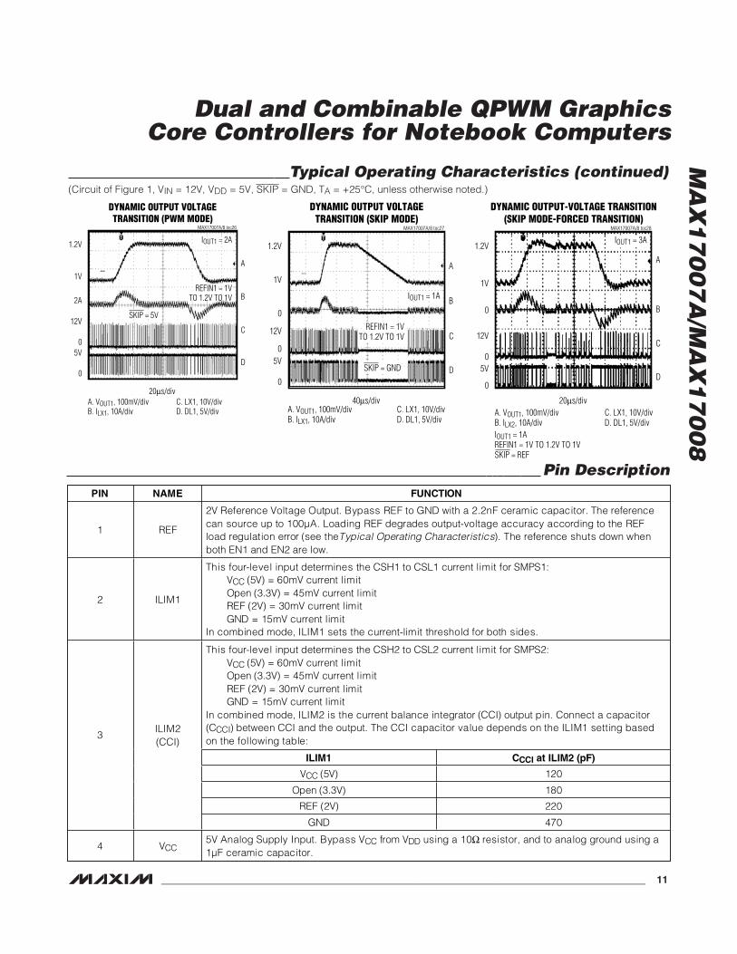
______________________________________________________________________________________ 11
DYNAMIC OUTPUT VOLTAGETRANSITION (PWM MODE)
MAX17007A/8 toc26
20μs/div
A
B
C
D
IOUT1 = 2A
REFIN1 = 1VTO 1.2V TO 1V
1.2V
1V
0
2A
12V
0
5V
A. VOUT1, 100mV/divB. ILX1, 10A/div
C. LX1, 10V/divD. DL1, 5V/div
SKIP = 5V
DYNAMIC OUTPUT VOLTAGETRANSITION (SKIP MODE)
MAX17007A/8 toc27
40μs/div
A
B
C
D
IOUT1 = 1A
1.2V
1V
0
0
12V
0
5V
A. VOUT1, 100mV/divB. ILX1, 10A/div
C. LX1, 10V/divD. DL1, 5V/div
REFIN1 = 1VTO 1.2V TO 1V
SKIP = GND
DYNAMIC OUTPUT-VOLTAGE TRANSITION(SKIP MODE-FORCED TRANSITION)
MAX17007A/8 toc28
20μs/div
A
B
C
D
1.2V
1V
0
0
12V
0
5V
A. VOUT1, 100mV/divB. ILX2, 10A/divIOUT1 = 1AREFIN1 = 1V TO 1.2V TO 1VSKIP = REF
C. LX1, 10V/divD. DL1, 5V/div
IOUT1 = 3A
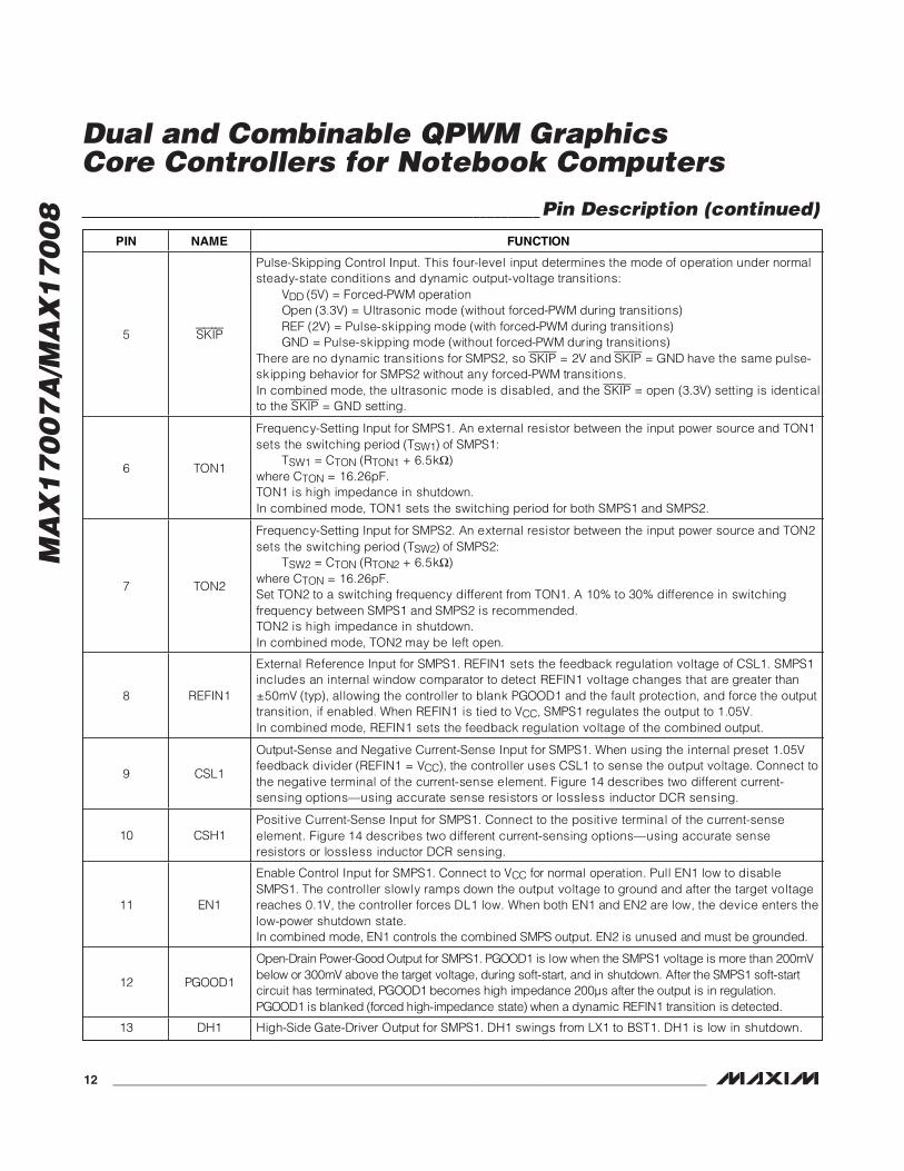
Pin Description
Typical Operating Characteristics (continued)(Circuit of Figure 1, VIN = 12V, VDD = 5V, SKIP = GND, TA = +25°C, unless otherwise noted.)
PIN NAME FUNCTION
1 REF
2V Reference Voltage Output. Bypass REF to GND with a 2.2nF ceramic capacitor. The reference can source up to 100μA. Loading REF degrades output-voltage accuracy according to the REF load regulation error (see theTypical Operating Characteristics). The reference shuts down when both EN1 and EN2 are low.
2 ILIM1
This four-level input determines the CSH1 to CSL1 current limit for SMPS1: VCC (5V) = 60mV current limit Open (3.3V) = 45mV current limit REF (2V) = 30mV current limit GND = 15mV current limit
In combined mode, ILIM1 sets the current-limit threshold for both sides.
This four-level input determines the CSH2 to CSL2 current limit for SMPS2: VCC (5V) = 60mV current limit Open (3.3V) = 45mV current limit REF (2V) = 30mV current limit GND = 15mV current limit
In combined mode, ILIM2 is the current balance integrator (CCI) output pin. Connect a capacitor (CCCI) between CCI and the output. The CCI capacitor value depends on the ILIM1 setting based on the following table:
ILIM1 CCCI at ILIM2 (pF)
VCC (5V) 120
Open (3.3V) 180
REF (2V) 220
3ILIM2 (CCI)
GND 470
4 VCC5V Analog Supply Input. Bypass VCC from VDD using a 10 resistor, and to analog ground using a 1μF ceramic capacitor.
MA
X1
70
07
A/M
AX
17
00
8
Dual and Combinable QPWM GraphicsCore Controllers for Notebook Computers
12 ______________________________________________________________________________________
Pin Description (continued)
PIN NAME FUNCTION
5 SKIP
Pulse-Skipping Control Input. This four-level input determines the mode of operation under normal steady-state conditions and dynamic output-voltage transitions:
VDD (5V) = Forced-PWM operation Open (3.3V) = Ultrasonic mode (without forced-PWM during transitions) REF (2V) = Pulse-skipping mode (with forced-PWM during transitions) GND = Pulse-skipping mode (without forced-PWM during transitions)
There are no dynamic transitions for SMPS2, so SKIP = 2V and SKIP = GND have the same pulse-skipping behavior for SMPS2 without any forced-PWM transitions. In combined mode, the ultrasonic mode is disabled, and the SKIP = open (3.3V) setting is identical to the SKIP = GND setting.
6 TON1
Frequency-Setting Input for SMPS1. An external resistor between the input power source and TON1 sets the switching period (TSW1) of SMPS1:
TSW1 = CTON (RTON1 + 6.5k )where CTON = 16.26pF. TON1 is high impedance in shutdown. In combined mode, TON1 sets the switching period for both SMPS1 and SMPS2.
7 TON2
Frequency-Setting Input for SMPS2. An external resistor between the input power source and TON2 sets the switching period (TSW2) of SMPS2:
TSW2 = CTON (RTON2 + 6.5k )where CTON = 16.26pF. Set TON2 to a switching frequency different from TON1. A 10% to 30% difference in switching frequency between SMPS1 and SMPS2 is recommended. TON2 is high impedance in shutdown. In combined mode, TON2 may be left open.
8 REFIN1
External Reference Input for SMPS1. REFIN1 sets the feedback regulation voltage of CSL1. SMPS1 includes an internal window comparator to detect REFIN1 voltage changes that are greater than ±50mV (typ), allowing the controller to blank PGOOD1 and the fault protection, and force the output transition, if enabled. When REFIN1 is tied to VCC, SMPS1 regulates the output to 1.05V. In combined mode, REFIN1 sets the feedback regulation voltage of the combined output.
9 CSL1
Output-Sense and Negative Current-Sense Input for SMPS1. When using the internal preset 1.05V feedback divider (REFIN1 = VCC), the controller uses CSL1 to sense the output voltage. Connect to the negative terminal of the current-sense element. Figure 14 describes two different current-sensing options—using accurate sense resistors or lossless inductor DCR sensing.
10 CSH1 Positive Current-Sense Input for SMPS1. Connect to the positive terminal of the current-sense element. Figure 14 describes two different current-sensing options—using accurate sense resistors or lossless inductor DCR sensing.
11 EN1
Enable Control Input for SMPS1. Connect to VCC for normal operation. Pull EN1 low to disable SMPS1. The controller slowly ramps down the output voltage to ground and after the target voltage reaches 0.1V, the controller forces DL1 low. When both EN1 and EN2 are low, the device enters the low-power shutdown state. In combined mode, EN1 controls the combined SMPS output. EN2 is unused and must be grounded.
12 PGOOD1
Open-Drain Power-Good Output for SMPS1. PGOOD1 is low when the SMPS1 voltage is more than 200mV below or 300mV above the target voltage, during soft-start, and in shutdown. After the SMPS1 soft-start circuit has terminated, PGOOD1 becomes high impedance 200μs after the output is in regulation. PGOOD1 is blanked (forced high-impedance state) when a dynamic REFIN1 transition is detected.
13 DH1 High-Side Gate-Driver Output for SMPS1. DH1 swings from LX1 to BST1. DH1 is low in shutdown.
MA
X1
70
07
A/M
AX
17
00
8
Dual and Combinable QPWM GraphicsCore Controllers for Notebook Computers
______________________________________________________________________________________ 13
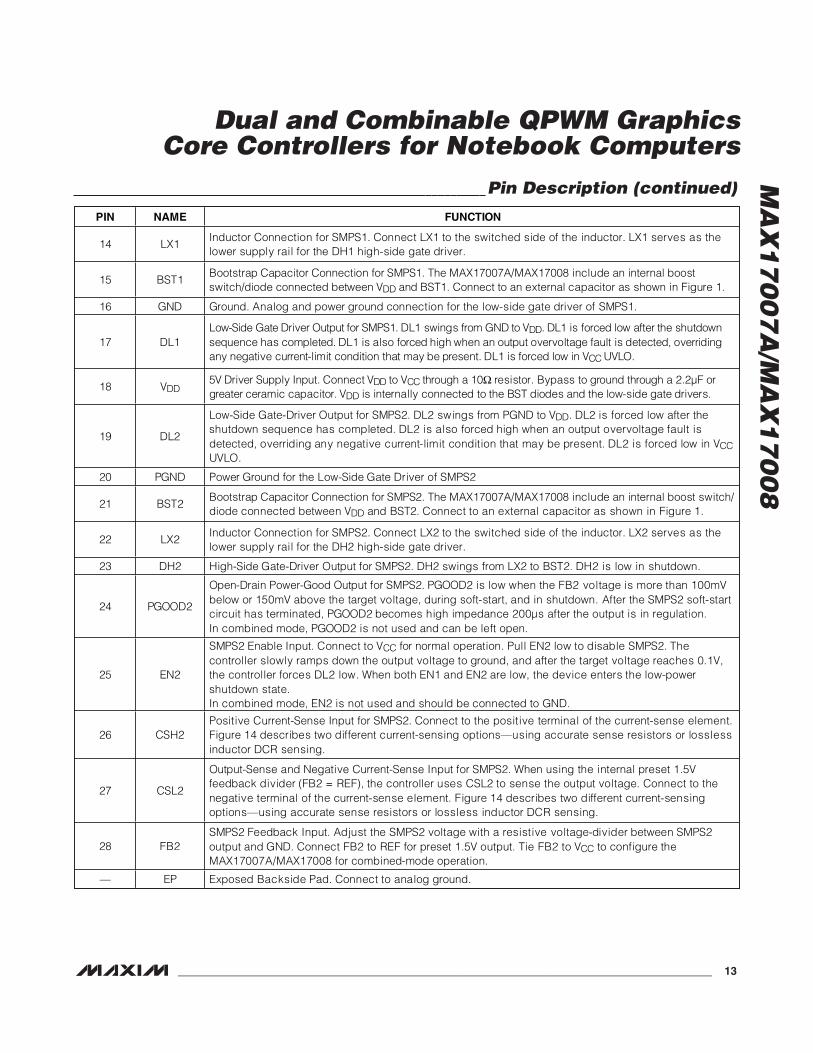
Pin Description (continued)
PIN NAME FUNCTION
14 LX1 Inductor Connection for SMPS1. Connect LX1 to the switched side of the inductor. LX1 serves as the lower supply rail for the DH1 high-side gate driver.
15 BST1 Bootstrap Capacitor Connection for SMPS1. The MAX17007A/MAX17008 include an internal boost switch/diode connected between VDD and BST1. Connect to an external capacitor as shown in Figure 1.
16 GND Ground. Analog and power ground connection for the low-side gate driver of SMPS1.
17 DL1 Low-Side Gate Driver Output for SMPS1. DL1 swings from GND to VDD. DL1 is forced low after the shutdown sequence has completed. DL1 is also forced high when an output overvoltage fault is detected, overriding any negative current-limit condition that may be present. DL1 is forced low in VCC UVLO.
18 VDD5V Driver Supply Input. Connect VDD to VCC through a 10 resistor. Bypass to ground through a 2.2μF or greater ceramic capacitor. VDD is internally connected to the BST diodes and the low-side gate drivers.
19 DL2
Low-Side Gate-Driver Output for SMPS2. DL2 swings from PGND to VDD. DL2 is forced low after the shutdown sequence has completed. DL2 is also forced high when an output overvoltage fault is detected, overriding any negative current-limit condition that may be present. DL2 is forced low in VCCUVLO.
20 PGND Power Ground for the Low-Side Gate Driver of SMPS2
21 BST2 Bootstrap Capacitor Connection for SMPS2. The MAX17007A/MAX17008 include an internal boost switch/ diode connected between VDD and BST2. Connect to an external capacitor as shown in Figure 1.
22 LX2 Inductor Connection for SMPS2. Connect LX2 to the switched side of the inductor. LX2 serves as the lower supply rail for the DH2 high-side gate driver.
23 DH2 High-Side Gate-Driver Output for SMPS2. DH2 swings from LX2 to BST2. DH2 is low in shutdown.
24 PGOOD2
Open-Drain Power-Good Output for SMPS2. PGOOD2 is low when the FB2 voltage is more than 100mV below or 150mV above the target voltage, during soft-start, and in shutdown. After the SMPS2 soft-start circuit has terminated, PGOOD2 becomes high impedance 200μs after the output is in regulation. In combined mode, PGOOD2 is not used and can be left open.
25 EN2
SMPS2 Enable Input. Connect to VCC for normal operation. Pull EN2 low to disable SMPS2. The controller slowly ramps down the output voltage to ground, and after the target voltage reaches 0.1V, the controller forces DL2 low. When both EN1 and EN2 are low, the device enters the low-power shutdown state. In combined mode, EN2 is not used and should be connected to GND.
26 CSH2 Positive Current-Sense Input for SMPS2. Connect to the positive terminal of the current-sense element. Figure 14 describes two different current-sensing options—using accurate sense resistors or lossless inductor DCR sensing.
27 CSL2
Output-Sense and Negative Current-Sense Input for SMPS2. When using the internal preset 1.5V feedback divider (FB2 = REF), the controller uses CSL2 to sense the output voltage. Connect to the negative terminal of the current-sense element. Figure 14 describes two different current-sensing options—using accurate sense resistors or lossless inductor DCR sensing.
28 FB2 SMPS2 Feedback Input. Adjust the SMPS2 voltage with a resistive voltage-divider between SMPS2 output and GND. Connect FB2 to REF for preset 1.5V output. Tie FB2 to VCC to configure the MAX17007A/MAX17008 for combined-mode operation.
— EP Exposed Backside Pad. Connect to analog ground.
MA
X1
70
07
A/M
AX
17
00
8
Dual and Combinable QPWM GraphicsCore Controllers for Notebook Computers
14 ______________________________________________________________________________________
MAX17007AMAX17008
6TON1
AGND
RREFIN1
RREFIN2
16
CVCC1μF
R2100kΩ
TO SYSTEMPOWER-GOOD
R910Ω
RTON1220kΩ
RNTC110kΩ
R43.01kΩ
RTON2180kΩ
CREF2.2nF
RREFIN3
GND
PWR
PWR
PWR
AGND
PWR
AGND
2ILIM1
3ILIM2(CCI)
5SKIP
11EN1
25EN2
1REF
RREFIN1 = 80.6kΩRREFIN2 = 121kΩRREFIN3 = 249kΩ 8
REFIN1
12PGOOD1
24PGOOD2
7TON2
15BST1
13DH1
14LX1
17DL1
NH1
NL120PGND
10CSH1
9CSL1
28FB2
4VCC
18VDD
REF
REF
+3.3V
H = 1.0VL = 1.2V
4-LEVEL SKIP PIN
REF
+5V
CONNECT TO REF FORFIXED 1.5V OUTPUT
*LOWER INPUT VOLTAGES REQUIREADDITIONAL INPUT CAPACITANCE.
VIN7V TO 20V
EP
POWER GROUND
ANALOG GROUND
R1100kΩ
CVDD2.2μF
C10.22μF
CBST10.1μF
PWR
DL1
CIN1
R31.5kΩ
COUT12 x 330μF12mΩ
L11μH, 16A, 3mΩ
VOUT11.2V/1.0V, 12A
ILIM1ILIM2
VCCOPENREFGND
R710Ω
C21nF
PWR
COUT1-CER5 x 10μFCERAMIC
VOUT21.5V, 12A
RNTC210kΩ
R63.01kΩ
PWR
AGND
PWR
21BST2
23DH2
22LX2
19DL2
NH2
NL2
26CSH2
27CSL2
VIN7V TO 20V
C30.22μF
CBST20.1μF
PWR
DL2
CIN2
R51.5kΩ
COUT22 x 330μF12mΩ
L21μH, 16A, 3mΩ
R810Ω
C41nF
PWR
COUT2-CER5 x 10μFCERAMIC
CURRENTLIMIT
60mV45mV30mV15mV
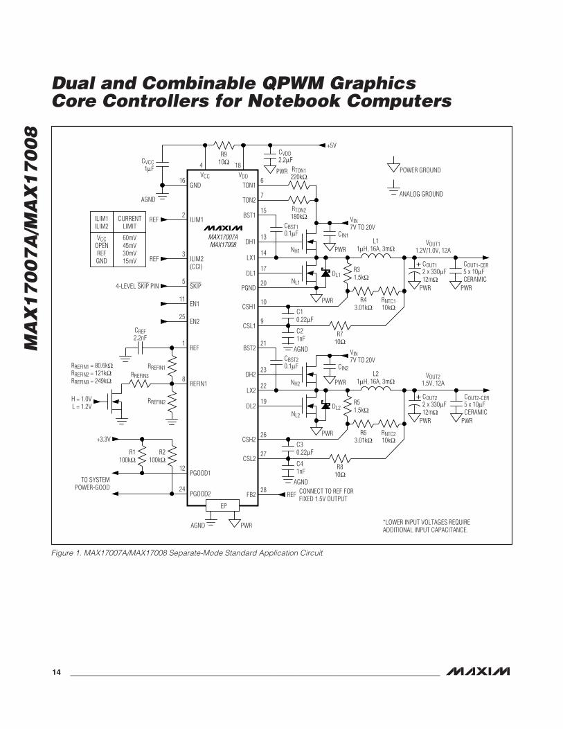
Figure 1. MAX17007A/MAX17008 Separate-Mode Standard Application Circuit
MA
X1
70
07
A/M
AX
17
00
8
Dual and Combinable QPWM GraphicsCore Controllers for Notebook Computers
______________________________________________________________________________________ 15
VOUT1 = 1.0V/1.2V AT 12A (FIGURE 1)
VOUT = 1.5V AT 12A (FIGURE 1)
COMPONENTVIN = 7V to 20V TON1 = 220k (270kHz)
VIN = 7V to 20V TON2 = 180k (330kHz)
Input Capacitor (per Phase)
(2x) 10μF, 25V Taiyo Yuden TMK432BJ106KM
(2x) 10μF, 25V Taiyo Yuden TMK432BJ106KM
Output Capacitor (2x) 330μF, 2.5V, 12m , C case SANYO 2R5TPE330MCC2
(2x) 330μF, 2.5V, 12m , C case SANYO 2R5TPE330MCC2
Inductor 1μH, 3.25m , 16A Würth Electronics 7443552100
1μH, 3.25m , 16A Würth Electronics 7443552100
Schottky Diode
2A, 30V Schottky diode (SMA) Nihon EC21QS03L Central Semiconductor CMSH2-40M
2A, 30V Schottky diode (SMA) Nihon EC21QS03L Central Semiconductor CMSH2-40M
High-Side MOSFET Fairchild Semiconductor (1x) FDS8690 8.6m /11.4m (typ/max)
Fairchild Semiconductor (1x) FDS8690 8.6m /11.4m (typ/max)
Low-Side MOSFET Fairchild Semiconductor (1x) FDS8670 4.2m /5m (typ/max)
Fairchild Semiconductor (1x) FDS8670 4.2m /5m (typ/max)
Table 1. Component Selection for Standard Applications
MANUFACTURER WEBSITE MANUFACTURER WEBSITE
AVX Corp. www.avxcorp.com Pulse Engineering www.pulseeng.com
BI Technologies www.bitechnologies.com Renesas Technology Corp. www.renesas.com
Central Semiconductor Corp. www.centralsemi.com SANYO Electric Company, Ltd. www.sanyodevice.com
Fairchild Semiconductor www.fairchildsemi.com Siliconix (Vishay) www.vishay.com
International Rectifier www.irf.com Sumida Corp. www.sumida.com
KEMET Corp. www.kemet.com Taiyo Yuden www.t-yuden.com
NEC TOKIN America, Inc. www.nec-tokinamerica.com TDK Corp. www.component.tdk.com
Panasonic Corp. www.panasonic.com TOKO America, Inc. www.tokoam.com
Table 2. Component Suppliers
Detailed DescriptionThe MAX17007A/MAX17008 standard application circuit(Figure 1) generates the 1V to 1.2V/12A and 1.5V/12Achipset voltages in a notebook computer. The input sup-ply range is 7V to 20V for the specific application. Table 1lists component selections, while Table 2 lists the com-ponent manufacturers. Figure 2 shows the combined-mode standard application circuit and Figure 3 is theMAX17007A/MAX17008 functional diagram.
The MAX17007A/MAX17008 contain two constant on-time step-down controllers designed for low-voltagepower supplies. The two SMPSs can also be combinedto operate as a two-phase high-current single-outputregulator. Constant on-time Quick-PWM operation pro-vides fast response to load transients and handles wide
I/O voltage ratios with ease, while maintaining a relativelyconstant switching frequency. The switching frequencycan be adjusted between 200kHz and 600kHz withexternal resistors. Differential output current sensingallows output sense-resistor sensing for an accurate cur-rent-limit, lossless inductor DCR current sensing for lowerpower dissipation while maintaining 0.7% output accura-cy. Overvoltage (MAX17007A) and undervoltage protec-tion and accurate user-selectable current limits (fourdifferent levels) ensure robust operations.
The MAX17007A/MAX17008 feature a special com-bined-mode configuration that allows higher currentoutputs to be supported. A current-balance integratormaintains equal currents in the two phases, improvingefficiency and power distribution.
MA
X1
70
07
A/M
AX
17
00
8
Dual and Combinable QPWM GraphicsCore Controllers for Notebook Computers
16 ______________________________________________________________________________________
MAX17007AMAX17008
6
X
TON1
AGND
RREFIN1
RREFIN2
16
CVCC1μF
PGOOD2 NOT USEDIIN COMBINED MODE
ILIM2 FUNCTIONS ASCCI OUTPUT IN
COMBINED MODE
EN2 MUST BEGROUNDED
R910Ω
RTON1220kΩ
RNTC110kΩ
R43.01kΩ
CREF2.2nF
CCCI220pF
RREFIN3
GND
PWR
PWR
PWR
AGND
PWR
AGND
2ILIM1
3ILIM2(CCI)
5SKIP
11EN1
25EN2
1REF
RREFIN1 = 80.6kΩRREFIN2 = 121kΩRREFIN3 = 249kΩ 8
REFIN1
12PGOOD1
24PGOOD2
7TON2
15BST1
13DH1
14LX1
17DL1
NH1
NL120PGND
10CSH1
9CSL1
28FB2
4VCC
18VDD
REF
VOUT
+3.3V
H = 1.0VL = 1.2V
+5V
+5V
CONNECT TO 5V FORCOMBINED MODE OPERATION
*LOWER INPUT VOLTAGES REQUIREADDITIONAL INPUT CAPACITANCE.
VIN7V TO 20V
EP
POWER GROUND
ANALOG GROUND
R1100kΩ
CVDD2.2μF
C10.22μF
CBST10.1μF
PWR
DL1
CIN1
R31.5kΩ
COUT14 x 330μF12mΩ
L11μH, 16A, 3mΩ
VOUT11.2V/1.0V, 24A
ILIMPIN
VCCOPENREFGND
R710Ω
C21nF
PWR
COUT1-CER10 x 10μFCERAMIC
RNTC210kΩ
R63.01kΩ
PWR
AGND
21BST2
23DH2
22LX2
19DL2
NH2
NL2
26CSH2
27CSL2
VIN7V TO 20V
C30.22μF
CBST20.1μF
PWR
DL2
CIN2
R51.5kΩ
L21μH, 16A, 3mΩ
R810Ω
C41nF
CURRENTLIMIT
CCCI(pF)
60mV45mV30mV15mV
120180220470
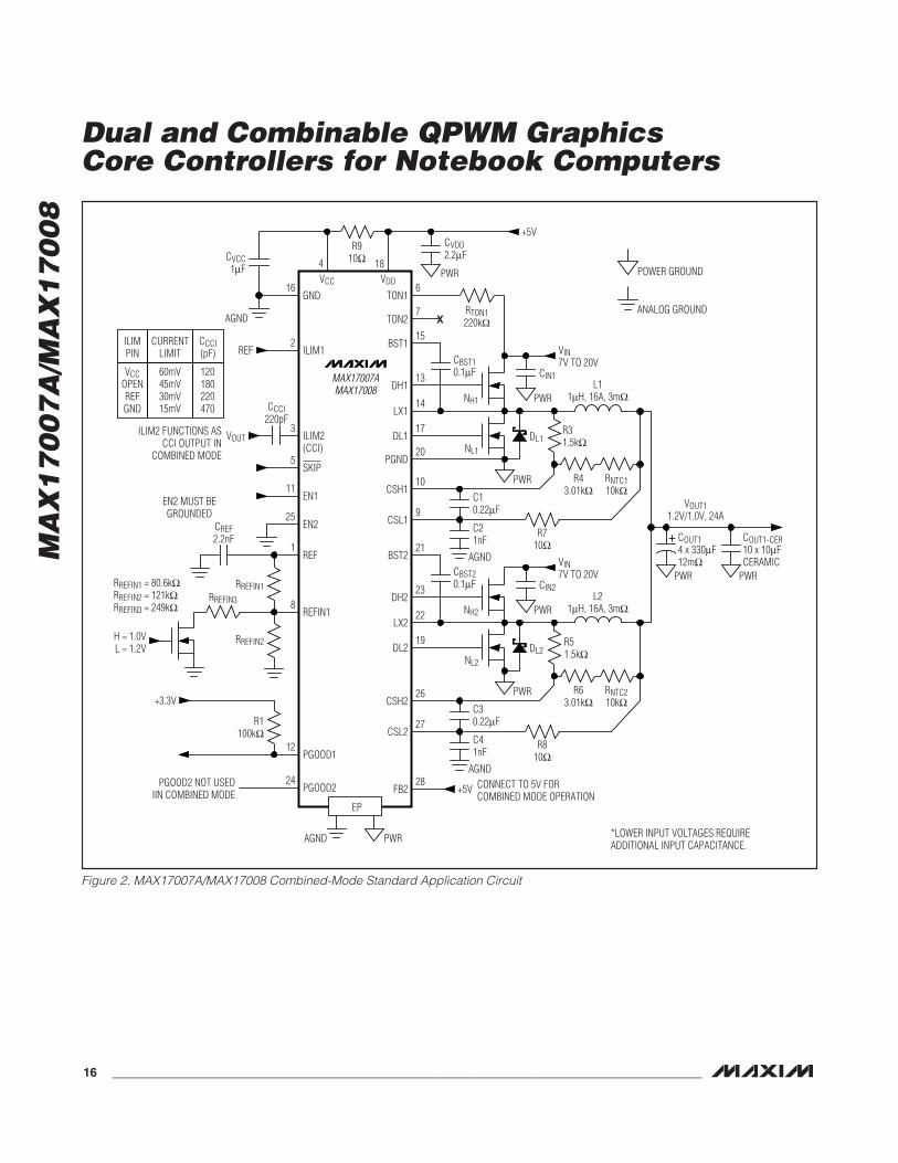
Figure 2. MAX17007A/MAX17008 Combined-Mode Standard Application Circuit
MA
X1
70
07
A/M
AX
17
00
8
Dual and Combinable QPWM GraphicsCore Controllers for Notebook Computers
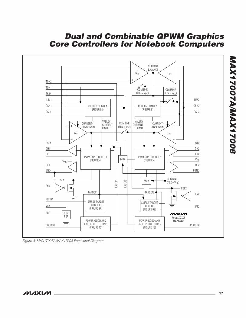
______________________________________________________________________________________ 17
MAX17007AMAX17008POWER-GOOD AND
FAULT PROTECTION 2(FIGURE 13)
PWM CONTROLLER 2(FIGURE 4)
CURRENT LIMIT 2(FIGURE 8)
SMPS2 TARGETDECODE
(FIGURE 9B)
MUX
2.0VREF
PGOOD2
COMBINE(FB2 = VCC)
FB2
CSH2
CSL2
ILIM2
EN2
LX2
CURRENT-SENSE GAIN
VALLEYCURRENT
LIMIT
DH2
BST2
PGND
DL2
VDD
CSL2TARGET2
Gm
Gm
POWER-GOOD ANDFAULT PROTECTION 1
(FIGURE 13)
PWM CONTROLLER 1(FIGURE 4)
CURRENT LIMIT 1(FIGURE 8)
SMPS1 TARGETDECODE
(FIGURE 9A)
MUX
PGOOD1
REF
VCC
REFIN1
CSH1
CSL1
ILIM1
SKIP
TON1
TON2
EN1
LX1
CURRENT-SENSE GAIN
VALLEYCURRENTLIMIT
DH1
BST1
GND
DL1
CSL1
Gm
Gm
TARGET1
FAUL
T1
FAUL
T2
VDD
CURRENTBALANCE
COMBINE(FB2 = VCC)
COMBINE(FB2 = VCC)
COMBINE(FB2 = VCC)
Figure 3. MAX17007A/MAX17008 Functional Diagram
+5V Bias Supply (VCC, VDD)The MAX17007A/MAX17008 require an external 5V biassupply in addition to the battery. Typically, this 5V biassupply is the notebook’s 95%-efficient 5V system sup-ply. Keeping the bias supply external to the IC improvesefficiency and eliminates the cost associated with the 5Vlinear regulator that would otherwise be needed to sup-ply the PWM circuit and gate drivers. If stand-alonecapability is needed, the 5V supply can be generatedwith an external linear regulator such as the MAX1615.
The 5V bias supply powers both the PWM controllersand internal gate-drive power, so the maximum currentdrawn depends on the external MOSFET’s gate capaci-tance, and the selected switching frequency:
IBIAS = IQ + fSW1QG(SMPS1) + fSW2QG(SMPS2)
= 4mA to 40mA (typ)
Bypass VCC with a 1μF or greater ceramic capacitor tothe analog ground. Bypass VDD with a 2.2μF or greaterceramic capacitor to the power ground. VCC and VDDshould be separated with a 10Ω resistor (Figure 1).
2V ReferenceThe 2V reference is accurate to ±1% over temperatureand load, making REF useful as a precision system ref-erence. Bypass REF to GND with a 2.2nF. The refer-ence sources up to 100μA and sinks 10μA to supportexternal loads.
Combined-Mode Operation (FB2 = VCC)Combined-mode operation allows the MAX17007A/MAX17008 to support even higher output currents bysharing the load current between two phases, distribut-ing the power dissipation over several power compo-nents to improve the efficiency. The MAX17007A/MAX17008 are configured in combined mode by con-necting FB2 to VCC. See Figure 2 for the combined-mode standard application circuit.
Table 3 lists the pin function differences between com-bined mode and separate mode. See the Pin Descriptionfor additional details.
MA
X1
70
07
A/M
AX
17
00
8
Dual and Combinable QPWM GraphicsCore Controllers for Notebook Computers
18 ______________________________________________________________________________________
PIN COMBINED MODE SEPARATE MODE
FB2 Connect to VCC to configure MAX17007A/MAX17008 for combined-mode operation
Connect to REF for preset 1.5V, or use a resistor-divider to set the SMPS2 output voltage
REFIN1 Sets the combined output voltage—dynamic, fixed, and preset voltages supported
Sets the SMPS1 output voltage—dynamic, fixed, and preset voltages supported
EN1 Enables/disables combined output Enables/disables SMPS1
EN2 Not used; connect to GND Enables/disables SMPS2
PGOOD1 Power-good indicator for combined output voltage Power-good indicator for SMPS1
PGOOD2 Not used; can be left open Power-good indicator for SMPS2
TON1 Sets the per-phase switching frequency for both SMPSs Sets the switching frequency for SMPS1
TON2 Not used; leave open Sets the switching frequency for SMPS2
ILIM1 Sets the per-phase current limit for both SMPSs Sets SMPS1 current limit
ILIM2 (CCI) Current-balance integrator output; connect a capacitor from CCI to the output
Sets SMPS2 current limit
SKIPOnly three distinct modes of operation; ultrasonic mode not supported
Supports all four modes of operation
Table 3. Pin Function in Combined and Separate Modes
MA
X1
70
07
A/M
AX
17
00
8
Dual and Combinable QPWM GraphicsCore Controllers for Notebook Computers
______________________________________________________________________________________ 19
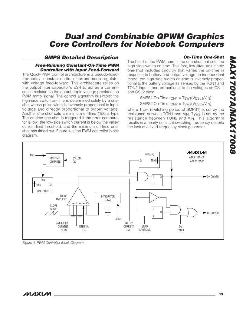
SMPS Detailed DescriptionFree-Running Constant-On-Time PWM
Controller with Input Feed-ForwardThe Quick-PWM control architecture is a pseudo-fixed-frequency, constant-on-time, current-mode regulatorwith voltage feed-forward. This architecture relies onthe output filter capacitor’s ESR to act as a current-sense resistor, so the output ripple voltage provides thePWM ramp signal. The control algorithm is simple: thehigh-side switch on-time is determined solely by a one-shot whose pulse width is inversely proportional to inputvoltage and directly proportional to output voltage.Another one-shot sets a minimum off-time (150ns typ).The on-time one-shot is triggered if the error compara-tor is low, the low-side switch current is below the valleycurrent-limit threshold, and the minimum off-time one-shot has timed out. Figure 4 is the PWM controller blockdiagram.
On-Time One-ShotThe heart of the PWM core is the one-shot that sets thehigh-side switch on-time. This fast, low-jitter, adjustableone-shot includes circuitry that varies the on-time inresponse to battery and output voltage. In independentmode, the high-side switch on-time is inversely propor-tional to the battery voltage as sensed by the TON1 andTON2 inputs, and proportional to the voltages on CSL1and CSL2 pins:
SMPS1 On-Time tON1 = TSW1(VCSL1/VIN)
SMPS2 On-Time tON2 = TSW2(VCSL2/VIN)
where TSW1 (switching period of SMPS1) is set by theresistance between TON1 and VIN, TSW2 is set by theresistance between TON2 and VIN. This algorithmresults in a nearly constant switching frequency despitethe lack of a fixed-frequency clock generator.
MAX17007AMAX17008
CSL ORCCI
DH DRIVER
DL DRIVER
ON-TIMECOMPUTE
INTEGRATOR(CCV)
TON
TRIG
ONE-SHOT
Q
ERRORAMPLIFIER
INTERNALFB
ZEROCROSSING
VALLEYCURRENT
LIMITOV
FAULT
AMPLIFIEDCURRENT
SENSE
SLOPECOMP
tON
R
S Q
R
SQ
TARGET
tOFF(MIN)
TRIGQ
Figure 4. PWM Controller Block Diagram
MA
X1
70
07
A/M
AX
17
00
8 Switching FrequencyThe MAX17007A/MAX17008 feature independent resis-tor-programmable switching frequencies for eachSMPS, providing flexibility for applications where oneSMPS operates at a lower switching frequency whenconnected to a high-voltage input rail while the otherSMPS operates at a higher switching frequency whenconnected to a lower voltage rail as a second-stageregulator. Connect a resistor (RTON) between TON andVIN to set the switching period TSW = 1/fSW:
TSW1 = CTON(RTON1 + 6.5kΩ)
TSW2 = CTON(RTON2 + 6.5kΩ)
where CTON = 16.26pF. A 97.5kΩ to 302.5kΩ corre-sponds to switching periods of 1.67μs (600kHz) to 5μs(200kHz) for SMPS1 and SMPS2. High-frequency(600kHz) operation optimizes the application for thesmallest component size, trading off efficiency due tohigher switching losses. This may be acceptable inultra-portable devices where the load currents arelower and the controller is powered from a lower volt-age supply. Low-frequency (200kHz) operation offersthe best overall efficiency at the expense of componentsize and board space.
For continuous conduction operation, the actual switchingfrequency can be estimated by:
where VDIS is the sum of the parasitic voltage drops inthe inductor discharge path, including synchronousrectifier, inductor, and printed-circuit board (PCB) resis-tances; VCHG is the sum of the resistances in thecharging path, including the high-side switch, inductor,and PCB resistances; and tON is the on-time calculatedby the on-time block.
When operating in separate mode, it is recommendedthat both SMPS switching frequencies be set apart by10% to 30% to prevent the two sides from beatingagainst each other.
Combined-Mode On-Time One-ShotIn combined mode (FB2 = VCC), TON1 sets the on-time, and hence the switching frequency, for both SMPS.The on-time is programmed using the TON1 equation,which sets the switching frequency per phase. The effec-tive switching frequency as seen on the input and outputcapacitors is twice the per-phase frequency.
Combined-Mode Current BalanceIn combined mode, the one-shot for SMPS2 varies theon-time in response to the input voltage and the differ-ence between the SMPS1 and SMPS2 inductor cur-rents. The SMPS1 one-shot in combined mode behavesthe same way as it does in separate mode. As such,SMPS2 regulates the current balance, while SMPS1regulates the voltage.
Two identical transconductance amplifiers integrate thedifference between SMPS1 and SMPS2 current-sensesignals. The summed output is internally connected toCCI, allowing adjustment of the integration time con-stant with a compensation network (usually a capacitor)connected between CCI and the output.
The resulting compensation current and voltage aredetermined by the following equations:
ICCI = Gm[(VCSH1 - VCSL1) - (VCSH2 - VCSL2)]
VCCI = VOUT + ICCIZCCI
where ZCCI is the impedance at the CCI output. TheSMPS2 on-time one-shot uses this integrated signal(VCCI) to set the SMPS2 high-side MOSFETs on-time.When SMPS1 and SMPS2 current-sense signals (VCSH1- VCSL1 and VCSH2 - VCSL2) become unbalanced, thetransconductance amplifiers adjust the SMPS2 on-time,which increases or decreases the SMPS2 inductor cur-rent until the current-sense signals are properly bal-anced. In combined mode, the SMPS2 on-time is givenby:
SMPS2 On-Time tON2 = TSW2(VCCI/VIN)
SMPS Enable Controls (EN1, EN2)EN1 and EN2 provide independent control of outputsoft-start and soft-shutdown. This allows flexible controlof startup and shutdown sequencing. The outputs canbe started simultaneously, sequentially, or indepen-dently. To provide sequential startup, connect EN ofone regulator to PGOOD of the other. For example, withEN1 connected to PGOOD2, OUT1 soft-starts afterOUT2 is in regulation.
When configured in separate mode, the two outputs areindependent. A fault at one output does not triggershutdown of the other.
When configured in combined mode (FB2 = VCC), EN1is the master control input that enables/disables thecombined output, while EN2 has no function and mustbe connected to GND. The startup slew rate followsthat of SMPS1.
Toggle EN low to clear the overvoltage, undervoltage,and thermal-fault latches.
fV V
t V VSWOUT DIS
ON IN CHG= +
+( )
Dual and Combinable QPWM GraphicsCore Controllers for Notebook Computers
20 ______________________________________________________________________________________
Soft-StartSoft-start begins when EN is driven high and REF is inregulation. During soft-start, the output is ramped upfrom 0V to the final set voltage at 1.3mV/μs slew rate forSMPS1, and 0.65mV/μs for SMPS2, reducing the inrushcurrent and providing a predictable ramp-up time forpower sequencing:
The soft-start circuitry does not use a variable currentlimit, so full output current is available immediately. Therespective PGOOD becomes high impedance approxi-mately 200μs after the target voltage has beenreached. The MAX17007A/MAX17008 automaticallyuse pulse-skipping mode during soft-start and useforced-PWM mode during soft-shutdown, regardless ofthe SKIP configuration.
For automatic startup, the battery voltage should bepresent before VCC. If the controller attempts to bringthe output into regulation without the battery voltagepresent, the fault latch trips. The controller remains shutdown until the fault latch is cleared by toggling EN orcycling the VCC power supply below 0.5V.
Soft-ShutdownSoft-shutdown begins when the system pulls EN low, anoutput undervoltage fault, or a thermal fault. Duringsoft-shutdown, the respective PGOOD is pulled lowimmediately and the output voltage ramps down withthe same startup slew rate for the respective outputs.After the controller reaches the 0V target, the driversare disabled (DL_ and DH_ pulled low) and the internal10Ω discharge on CSL_ activated. The MAX17007A/MAX17008 shut down completely when both EN arelow—the reference turns off after both SMPSs havereached the 0V target, and the supply current drops toabout 1μA (max).
Slowly discharging the output capacitors by slewing theoutput over a long period of time (typically 0.5ms to2ms) keeps the average negative inductor current low(damped response), thereby preventing the negativeoutput-voltage excursion that occurs when the con-troller discharges the output quickly by permanentlyturning on the low-side MOSFET (underdamped
response). This eliminates the need for the Schottkydiode normally connected between the output andground to clamp the negative output-voltage excursion.
Modes of OperationForced-PWM Mode (SSKKIIPP = 5V)
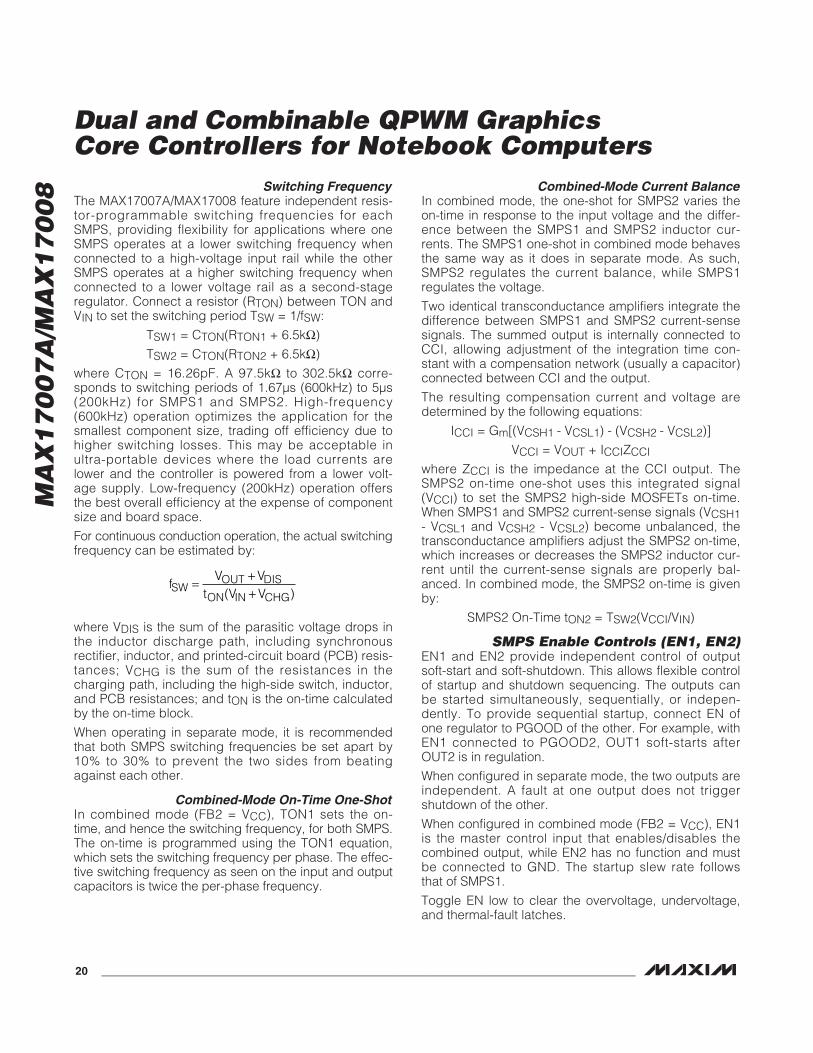
The low-noise forced-PWM mode (SKIP = 5V) disablesthe zero-crossing comparator, which controls the low-side switch on-time. This forces the low-side gate-drivewaveform to constantly be the complement of the high-side gate-drive waveform, so the inductor currentreverses at light loads while DH maintains a duty factorof VOUT/VIN. The benefit of forced-PWM mode is tokeep the switching frequency fairly constant. However,forced-PWM operation comes at a cost: the no-load 5Vbias current remains between 2mA to 5mA, dependingon the switching frequency.
The MAX17007A/MAX17008 automatically use forced-PWM operation during shutdown, regardless of theSKIP configuration.
Automatic Pulse-Skipping Mode(SSKKIIPP = GND or 2V)
In skip mode (SKIP = GND or 2V), an inherent automaticswitchover to PFM takes place at light loads. Thisswitchover is affected by a comparator that truncatesthe low-side switch on-time at the inductor current’szero crossing. The zero-crossing comparator thresholdis set by the differential across CSL_ and CSH_.
DC output-accuracy specifications refer to the threshold ofthe error comparator. When the inductor is in continuousconduction, the MAX17007A/MAX17008 regulate thevalley of the output ripple, so the actual DC output volt-age is higher than the trip level by 50% of the output rip-ple voltage. In discontinuous conduction (SKIP = GNDor 2V and IOUT < ILOAD(SKIP)), the output voltage has aDC regulation level higher than the error-comparatorthreshold by approximately 1.5% due to slope compen-sation. However, the internal integrator corrects for mostof it, resulting in very little load regulation.
When SKIP = 2V, the MAX17007A/MAX17008 use forced-PWM operation during all dynamic output-voltage transi-tions until 100μs after the transition has beencompleted—REFIN1 and the internal target are within±50mV (typ) and an error-amplifier transition is detected.Since SMPS2 does not support dynamic transitions, SKIP= 2V and SKIP = GND have the same pulse-skippingbehavior without any forced-PWM transitions.
t tV
SRV
mV μsSTART SHDNFB
SS
FB2 2
2
2
20 65
= = =.
t tVSR
VmV μsSTART SHDN
REFIN
SS
REFIN1 1
1
1
11 3
= = =.
MA
X1
70
07
A/M
AX
17
00
8
Dual and Combinable QPWM GraphicsCore Controllers for Notebook Computers
______________________________________________________________________________________ 21
MA
X1
70
07
A/M
AX
17
00
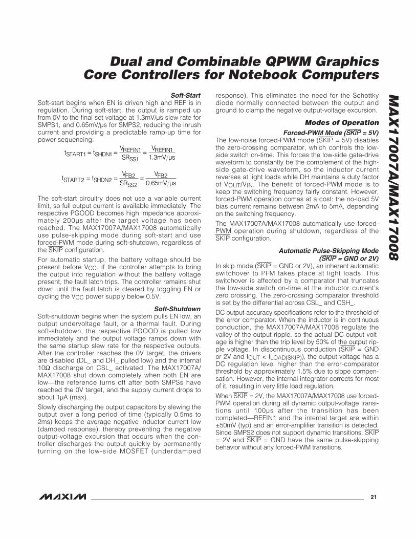
8 When SKIP is pulled to GND, the MAX17007A/MAX17008remain in pulse-skipping mode. Since the output is notable to sink current, the timing for negative dynamic out-put-voltage transitions depends on the load current andoutput capacitance. Letting the output voltage drift downis typically recommended in order to reduce the potentialfor audible noise since this eliminates the input currentsurge during negative output-voltage transitions. Figure 5shows the pulse-skipping/discontinuous crossover point.
Ultrasonic Mode (SSKKIIPP = Open = 3.3V)Leaving SKIP unconnected or connecting SKIP to 3.3Vactivates a unique pulse-skipping mode with a mini-mum switching frequency of 25kHz. This ultrasonicpulse-skipping mode eliminates audio-frequency mod-ulation that would otherwise be present when a lightlyloaded controller automatically skips pulses. In ultra-sonic mode, the controller automatically transitions tofixed-frequency PWM operation when the load reachesthe same critical conduction point (ILOAD(SKIP)) thatoccurs when normally pulse skipping.
An ultrasonic pulse occurs when the controller detectsthat no switching has occurred within the last 30μs.Once triggered, the ultrasonic controller pulls DL high,turning on the low-side MOSFET to induce a negativeinductor current (Figure 6). After the inductor currentreaches the negative ultrasonic current threshold, thecontroller turns off the low-side MOSFET (DL pulledlow) and triggers a constant on-time (DH driven high).When the on-time has expired, the controller reenablesthe low-side MOSFET until the controller detects thatthe inductor current dropped below the zero-crossingthreshold. Starting with a DL pulse greatly reduces thepeak output voltage when compared to starting with aDH pulse.
The output voltage at the beginning of the ultrasonicpulse determines the negative ultrasonic current thresh-old, resulting in the following equations for SMPS1:
(SMPS1 adjustable mode)
(SMPS1 preset mode)
where VCSL1 > VREFIN1 in adjustable mode, VCSL1 >1.05V in preset mode, and RCS1 is the current-senseresistance seen across CSH1 to CSL1.
Similarly for SMPS2:
(SMPS2 adjustable mode)
(SMPS2 preset mode)
where VCSL2 > 0.7V in adjustable mode, VCSL2 > 1.5Vin preset mode, and RCS2 is the current-sense resis-tance seen across CSH2 to CSL2.
In combined mode, ultrasonic mode setting is disabled,and the SKIP = open (3.3V) setting is identical to theSKIP = GND setting.
V I R V VISONIC L CS CSL2 2 2 21 5 0 65. .= = ( ) ×-
V I R V VISONIC L CS FB2 2 2 20 7 0 65. .= = ( ) ×-
V I R V VISONIC L CS CSL1 1 1 11 05 0 65. .= = ( ) ×-
V I R V VISONIC L CS REFIN CSL1 1 1 1 1 0 65.= = ( ) ×-
Dual and Combinable QPWM GraphicsCore Controllers for Notebook Computers
22 ______________________________________________________________________________________
INDU
CTOR
CUR
RENT
ILOAD = IPEAK/2
ON-TIME0 TIME
IPEAK
LVIN - VOUTΔI
Δt=
Figure 5. Pulse-Skipping/Discontinuous Crossover Point
ON-TIME (tON)ISONIC
0
ZERO-CROSSINGDETECTION
INDUCTORCURRENT
40μs (MAX)
Figure 6. Ultrasonic Waveform
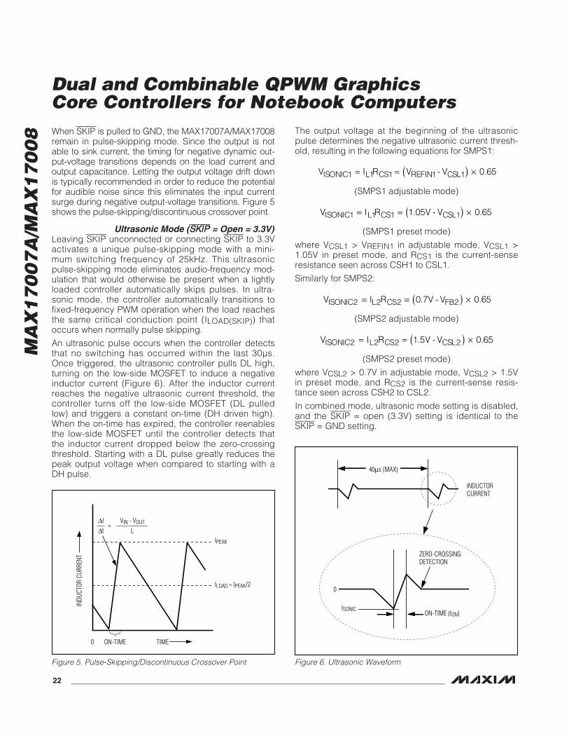
Valley Current-Limit ProtectionThe current-limit circuit employs a unique “valley” cur-rent-sensing algorithm that senses the inductor currentacross the output current-sense element—inductorDCR or current-sense resistor, which generates a volt-age between CSH_ and CSL_. If the current exceedsthe valley current-limit threshold during the low-sideMOSFET conduction time, the PWM controller is notallowed to initiate a new cycle. The valley current-limitthreshold is set by the four-level ILIM_ pin, with selec-table limits of 15mV, 30mV, 45mV, and 60mV.
The actual peak current is greater than the valley cur-rent-limit threshold by an amount equal to the inductorripple current (Figure 7). Therefore, the exact current-limit characteristic and maximum load capability are afunction of the inductor value and battery voltage.When combined with the undervoltage protection cir-cuit, this current-limit method is effective in almostevery circumstance. See Figure 8.
In forced-PWM mode, the MAX17007A/MAX17008 alsoimplement a negative current limit to prevent excessivereverse inductor currents when VOUT is sinking current.The negative current-limit threshold is set to approxi-mately 120% of the positive current limit.
In combined mode, ILIM1 sets the per-phase currentlimit for both phases.
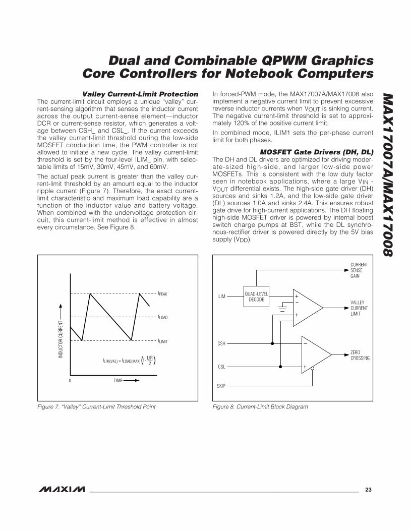
MOSFET Gate Drivers (DH, DL)The DH and DL drivers are optimized for driving moder-ate-sized high-side, and larger low-side powerMOSFETs. This is consistent with the low duty factorseen in notebook applications, where a large VIN -VOUT differential exists. The high-side gate driver (DH)sources and sinks 1.2A, and the low-side gate driver(DL) sources 1.0A and sinks 2.4A. This ensures robustgate drive for high-current applications. The DH floatinghigh-side MOSFET driver is powered by internal boostswitch charge pumps at BST, while the DL synchro-nous-rectifier driver is powered directly by the 5V biassupply (VDD).
MA
X1
70
07
A/M
AX
17
00
8
Dual and Combinable QPWM GraphicsCore Controllers for Notebook Computers
______________________________________________________________________________________ 23
INDU
CTOR
CUR
RENT
ILIMIT
ILOAD
0 TIME
IPEAK
ILIM(VAL) = ILOAD(MAX) 1- LIR2( )
Figure 7. “Valley” Current-Limit Threshold Point
CSH
ILIM
CSL
SKIP
ZEROCROSSING
VALLEYCURRENTLIMIT
QUAD-LEVELDECODE
CURRENT-SENSEGAIN
Figure 8. Current-Limit Block Diagram
MA
X1
70
07
A/M
AX
17
00
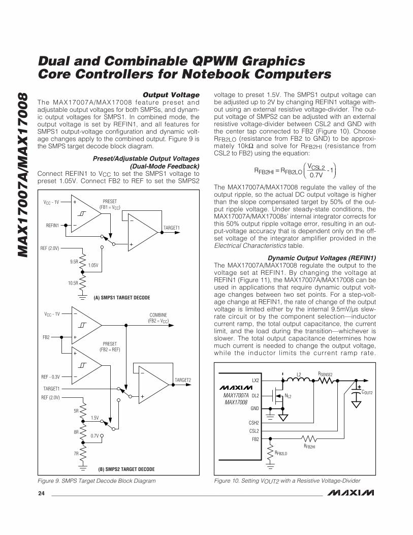
8 Output VoltageThe MAX17007A/MAX17008 feature preset andadjustable output voltages for both SMPSs, and dynam-ic output voltages for SMPS1. In combined mode, theoutput voltage is set by REFIN1, and all features forSMPS1 output-voltage configuration and dynamic volt-age changes apply to the combined output. Figure 9 isthe SMPS target decode block diagram.
Preset/Adjustable Output Voltages(Dual-Mode Feedback)
Connect REFIN1 to VCC to set the SMPS1 voltage topreset 1.05V. Connect FB2 to REF to set the SMPS2
voltage to preset 1.5V. The SMPS1 output voltage canbe adjusted up to 2V by changing REFIN1 voltage with-out using an external resistive voltage-divider. The out-put voltage of SMPS2 can be adjusted with an externalresistive voltage-divider between CSL2 and GND withthe center tap connected to FB2 (Figure 10). ChooseRFB2LO (resistance from FB2 to GND) to be approxi-mately 10kΩ and solve for RFB2HI (resistance fromCSL2 to FB2) using the equation:
The MAX17007A/MAX17008 regulate the valley of theoutput ripple, so the actual DC output voltage is higherthan the slope compensated target by 50% of the out-put ripple voltage. Under steady-state conditions, theMAX17007A/MAX17008s’ internal integrator corrects forthis 50% output ripple voltage error, resulting in an out-put-voltage accuracy that is dependent only on the off-set voltage of the integrator amplifier provided in theElectrical Characteristics table.
Dynamic Output Voltages (REFIN1)The MAX17007A/MAX17008 regulate the output to thevoltage set at REFIN1. By changing the voltage atREFIN1 (Figure 11), the MAX17007A/MAX17008 can beused in applications that require dynamic output volt-age changes between two set points. For a step-volt-age change at REFIN1, the rate of change of the outputvoltage is limited either by the internal 9.5mV/μs slew-rate circuit or by the component selection—inductorcurrent ramp, the total output capacitance, the currentlimit, and the load during the transition—whichever isslower. The total output capacitance determines howmuch current is needed to change the output voltage,while the inductor l imits the current ramp rate.
R RV
VFB HI FB LOCSL
2 22
0 71= ⎛
⎝⎜⎞⎠⎟.
-
Dual and Combinable QPWM GraphicsCore Controllers for Notebook Computers
24 ______________________________________________________________________________________
VCC - 1V
FB2
REF - 0.3V
TARGET1
COMBINE(FB2 = VCC)
PRESET(FB1 = VCC)
PRESET(FB2 = REF)
(B) SMPS2 TARGET DECODE
TARGET2
REF (2.0V)
0.7V
1.5V5R
8R
7R
REFIN1
(A) SMPS1 TARGET DECODE
TARGET1
REF (2.0V)
1.05V9.5R
10.5R
VCC - 1V
Figure 9. SMPS Target Decode Block Diagram
MAX17007AMAX17008
DL2
GND
LX2L2
FB2
CSL2
CSH2
RFB2LO
COUT2
RSENSE2
RFB2HI
NL2
Figure 10. Setting VOUT2 with a Resistive Voltage-Divider
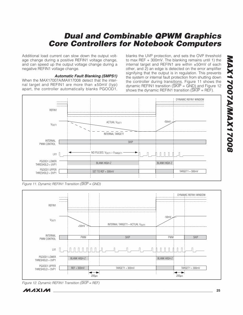
Additional load current can slow down the output volt-age change during a positive REFIN1 voltage change,and can speed up the output voltage change during anegative REFIN1 voltage change.
Automatic Fault Blanking (SMPS1)When the MAX17007A/MAX17008 detect that the inter-nal target and REFIN1 are more than ±50mV (typ)apart, the controller automatically blanks PGOOD1,
blanks the UVP protection, and sets the OVP thresholdto max REF + 300mV. The blanking remains until 1) theinternal target and REFIN1 are within ±50mV of eachother, and 2) an edge is detected on the error amplifiersignifying that the output is in regulation. This preventsthe system or internal fault protection from shutting downthe controller during transitions. Figure 11 shows thedynamic REFIN1 transition (SKIP = GND) and Figure 12shows the dynamic REFIN1 transition (SKIP = REF).
MA
X1
70
07
A/M
AX
17
00
8
Dual and Combinable QPWM GraphicsCore Controllers for Notebook Computers
______________________________________________________________________________________ 25
INTERNALPWM CONTROL
REFIN1
BLANK HIGH-Z
SKIP
LX1
SET TO REF + 300mV
VOUT1
INTERNAL TARGET1
ACTUAL VOUT1
BLANK HIGH-Z
DYNAMIC REFIN1 WINDOW
TARGET1 + 300mV
-50mV
PGOOD1 LOWERTHRESHOLD + UVP1
PGOOD1 UPPERTHRESHOLD + OVP1
NO PULSES: VOUT1 > VTARGET1
Figure 11. Dynamic REFIN1 Transition (SKIP = GND)
INTERNALPWM CONTROL
VOUT1
REFIN1
BLANK HIGH-Z
SKIP
LX1
REF + 300mV
INTERNAL TARGET1 = ACTUAL VOUT1
BLANK HIGH-Z
SKIP
200μs 200μs
+50mV
-50mV
PGOOD1 LOWERTHRESHOLD + UVP1
PGOOD1 UPPERTHRESHOLD + OVP1
PWM PWM
TARGET1 + 300mVTARGET1 + 300mV
DYNAMIC REFIN1 WINDOW
Figure 12. Dynamic REFIN1 Transition (SKIP = REF)
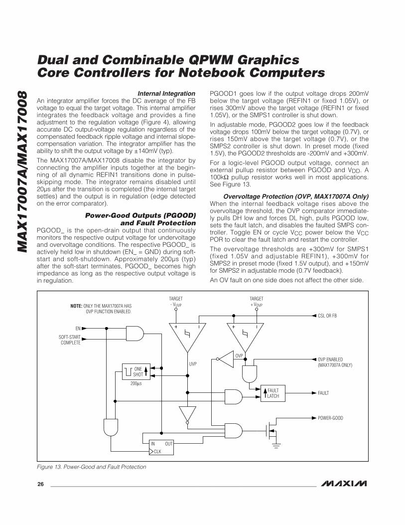
MA
X1
70
07
A/M
AX
17
00
8 Internal IntegrationAn integrator amplifier forces the DC average of the FBvoltage to equal the target voltage. This internal amplifierintegrates the feedback voltage and provides a fineadjustment to the regulation voltage (Figure 4), allowingaccurate DC output-voltage regulation regardless of thecompensated feedback ripple voltage and internal slope-compensation variation. The integrator amplifier has theability to shift the output voltage by ±140mV (typ).
The MAX17007A/MAX17008 disable the integrator byconnecting the amplifier inputs together at the begin-ning of all dynamic REFIN1 transitions done in pulse-skipping mode. The integrator remains disabled until20μs after the transition is completed (the internal targetsettles) and the output is in regulation (edge detectedon the error comparator).
Power-Good Outputs (PGOOD)and Fault Protection
PGOOD_ is the open-drain output that continuouslymonitors the respective output voltage for undervoltageand overvoltage conditions. The respective PGOOD_ isactively held low in shutdown (EN_ = GND) during soft-start and soft-shutdown. Approximately 200μs (typ)after the soft-start terminates, PGOOD_ becomes highimpedance as long as the respective output voltage isin regulation.
PGOOD1 goes low if the output voltage drops 200mVbelow the target voltage (REFIN1 or fixed 1.05V), orrises 300mV above the target voltage (REFIN1 or fixed1.05V), or the SMPS1 controller is shut down.
In adjustable mode, PGOOD2 goes low if the feedbackvoltage drops 100mV below the target voltage (0.7V), orrises 150mV above the target voltage (0.7V), or theSMPS2 controller is shut down. In preset mode (fixed1.5V), the PGOOD2 thresholds are -200mV and +300mV.
For a logic-level PGOOD output voltage, connect anexternal pullup resistor between PGOOD and VDD. A100kΩ pullup resistor works well in most applications.See Figure 13.
Overvoltage Protection (OVP, MAX17007A Only)When the internal feedback voltage rises above theovervoltage threshold, the OVP comparator immediate-ly pulls DH low and forces DL high, pulls PGOOD low,sets the fault latch, and disables the faulted SMPS con-troller. Toggle EN or cycle VCC power below the VCCPOR to clear the fault latch and restart the controller.
The overvoltage thresholds are +300mV for SMPS1(fixed 1.05V and adjustable REFIN1), +300mV forSMPS2 in preset mode (fixed 1.5V output), and +150mVfor SMPS2 in adjustable mode (0.7V feedback).
An OV fault on one side does not affect the other side.
Dual and Combinable QPWM GraphicsCore Controllers for Notebook Computers
26 ______________________________________________________________________________________
TARGET+ VOVP
TARGET- VUVP
CSL OR FB
FAULT
OVP ENABLED(MAX17007A ONLY)
FAULTLATCH
ONESHOT
200μs
POWER-GOOD
IN
CLK
OUT
OVP
UVP
EN
SOFT-STARTCOMPLETE
NOTE: ONLY THE MAX17007A HASOVP FUNCTION ENABLED.
Figure 13. Power-Good and Fault Protection
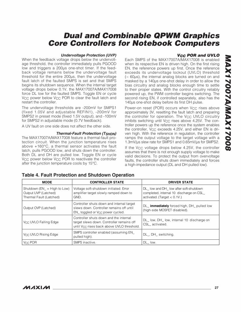
Undervoltage Protection (UVP)When the feedback voltage drops below the undervolt-age threshold, the controller immediately pulls PGOODlow and triggers a 200μs one-shot timer. If the feed-back voltage remains below the undervoltage faultthreshold for the entire 200μs, then the undervoltagefault latch of the faulted SMPS is set and that SMPSbegins its shutdown sequence. When the internal targetvoltage drops below 0.1V, the MAX17007A/MAX17008force DL low for the faulted SMPS. Toggle EN or cycleVCC power below VCC POR to clear the fault latch andrestart the controller.
The undervoltage thresholds are -200mV for SMPS1(fixed 1.05V and adjustable REFIN1), -200mV forSMPS2 in preset mode (fixed 1.5V output), and -100mVfor SMPS2 in adjustable mode (0.7V feedback).
A UV fault on one side does not affect the other side.
Thermal-Fault Protection (TSHDN)The MAX17007A/MAX17008 feature a thermal-fault pro-tection circuit. When the junction temperature risesabove +160°C, a thermal sensor activates the faultlatch, pulls PGOOD low, and shuts down the controller.Both DL and DH are pulled low. Toggle EN or cycleVCC power below VCC POR to reactivate the controllerafter the junction temperature cools by 15°C.
VCC POR and UVLOEach SMPS of the MAX17007A/MAX17008 is enabledwhen its respective EN is driven high. On the first risingEN, the reference powers up first. Once the referenceexceeds its undervoltage lockout (UVLO) threshold (~ 60μs), the internal analog blocks are turned on andmasked by a 140μs one-shot delay in order to allow thebias circuitry and analog blocks enough time to settleto their proper states. With the control circuitry reliablypowered up, the PWM controller begins switching. Thesecond rising EN, if controlled separately, also has the140μs one-shot delay before its first DH pulse.
Power-on reset (POR) occurs when VCC rises aboveapproximately 3V, resetting the fault latch and preparingthe controller for operation. The VCC UVLO circuitryinhibits switching until VCC rises above 4.25V. The con-troller powers up the reference once the system enablesthe controller, VCC exceeds 4.25V, and either EN is dri-ven high. With the reference in regulation, the controllerramps the output voltage to the target voltage with a1.3mV/μs slew rate for SMPS1 and 0.65mV/μs for SMPS2.
If the VCC voltage drops below 4.25V, the controllerassumes that there is not enough supply voltage to makevalid decisions. To protect the output from overvoltagefaults, the controller shuts down immediately and forcesa high-impedance output (DL and DH pulled low).
MA
X1
70
07
A/M
AX
17
00
8
Dual and Combinable QPWM GraphicsCore Controllers for Notebook Computers
______________________________________________________________________________________ 27
MODE CONTROLLER STATE DRIVER STATE
Shutdown (EN_ = High to Low) Output UVP (Latched) Thermal Fault (Latched)
Voltage soft-shutdown initiated. Error amplifier target slowly ramped down to GND.
DL_ low and DH_ low after soft-shutdown completed, internal 10 discharge on CSL_ activated. (Target < 0.1V.)
Output OVP (Latched) Controller shuts down and internal target slews down. Controller remains off until EN_ toggled or VCC power cycled.
DL_ immediately forced high, DH_ pulled low (high-side MOSFET disabled).
VCC UVLO Falling Edge Controller shuts down and the internal target slews down. Controller remains off until VCC rises back above UVLO threshold.
DL_ low, DH_ low, internal 10 discharge on CSL_ activated.
VCC UVLO Rising Edge SMPS controller enabled (assuming EN_ pulled high).
DL_, DH_ switching.
VCC POR SMPS inactive. DL_ low.
Table 4. Fault Protection and Shutdown Operation
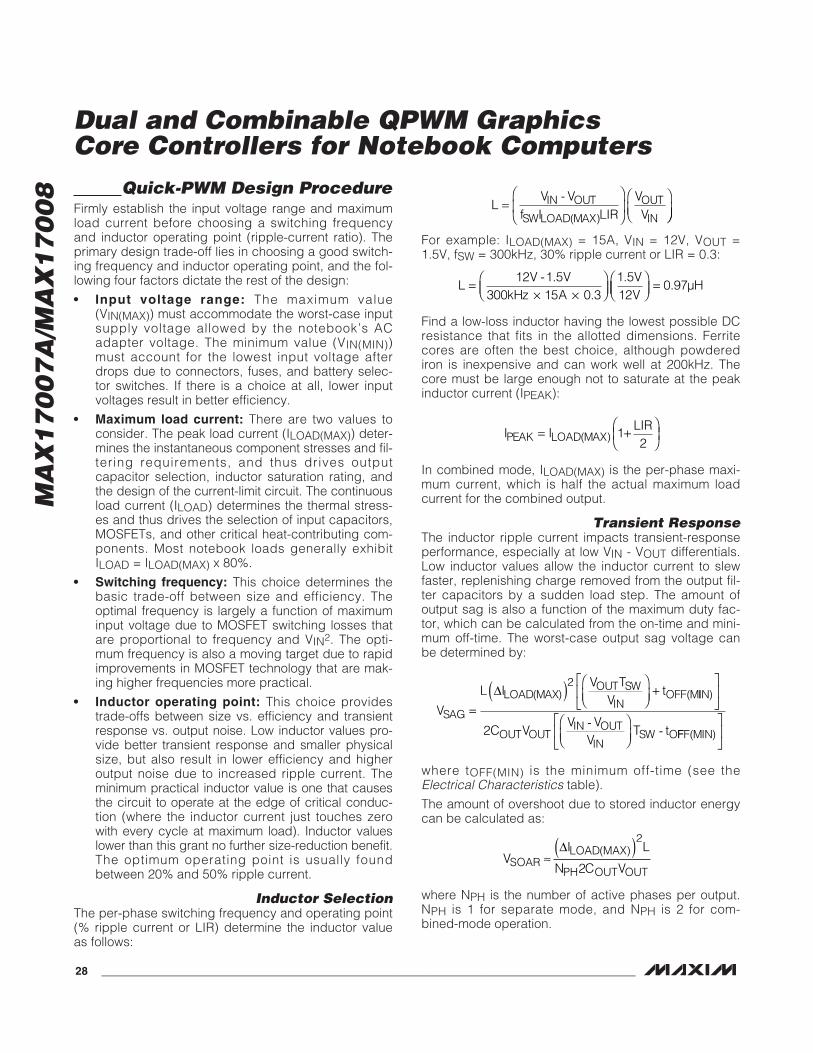
MA
X1
70
07
A/M
AX
17
00
8 Quick-PWM Design ProcedureFirmly establish the input voltage range and maximumload current before choosing a switching frequencyand inductor operating point (ripple-current ratio). Theprimary design trade-off lies in choosing a good switch-ing frequency and inductor operating point, and the fol-lowing four factors dictate the rest of the design:
• Input voltage range: The maximum value(VIN(MAX)) must accommodate the worst-case inputsupply voltage allowed by the notebook’s ACadapter voltage. The minimum value (VIN(MIN))must account for the lowest input voltage afterdrops due to connectors, fuses, and battery selec-tor switches. If there is a choice at all, lower inputvoltages result in better efficiency.
• Maximum load current: There are two values toconsider. The peak load current (ILOAD(MAX)) deter-mines the instantaneous component stresses and fil-tering requirements, and thus drives outputcapacitor selection, inductor saturation rating, andthe design of the current-limit circuit. The continuousload current (ILOAD) determines the thermal stress-es and thus drives the selection of input capacitors,MOSFETs, and other critical heat-contributing com-ponents. Most notebook loads generally exhibitILOAD = ILOAD(MAX) x 80%.
• Switching frequency: This choice determines thebasic trade-off between size and efficiency. Theoptimal frequency is largely a function of maximuminput voltage due to MOSFET switching losses thatare proportional to frequency and VIN2. The opti-mum frequency is also a moving target due to rapidimprovements in MOSFET technology that are mak-ing higher frequencies more practical.
• Inductor operating point: This choice providestrade-offs between size vs. efficiency and transientresponse vs. output noise. Low inductor values pro-vide better transient response and smaller physicalsize, but also result in lower efficiency and higheroutput noise due to increased ripple current. Theminimum practical inductor value is one that causesthe circuit to operate at the edge of critical conduc-tion (where the inductor current just touches zerowith every cycle at maximum load). Inductor valueslower than this grant no further size-reduction benefit.The optimum operating point is usually foundbetween 20% and 50% ripple current.
Inductor SelectionThe per-phase switching frequency and operating point(% ripple current or LIR) determine the inductor valueas follows:
For example: ILOAD(MAX) = 15A, VIN = 12V, VOUT =1.5V, fSW = 300kHz, 30% ripple current or LIR = 0.3:
Find a low-loss inductor having the lowest possible DCresistance that fits in the allotted dimensions. Ferritecores are often the best choice, although powderediron is inexpensive and can work well at 200kHz. Thecore must be large enough not to saturate at the peakinductor current (IPEAK):
In combined mode, ILOAD(MAX) is the per-phase maxi-mum current, which is half the actual maximum loadcurrent for the combined output.
Transient ResponseThe inductor ripple current impacts transient-responseperformance, especially at low VIN - VOUT differentials.Low inductor values allow the inductor current to slewfaster, replenishing charge removed from the output fil-ter capacitors by a sudden load step. The amount ofoutput sag is also a function of the maximum duty fac-tor, which can be calculated from the on-time and mini-mum off-time. The worst-case output sag voltage canbe determined by:
where tOFF(MIN) is the minimum off-time (see theElectrical Characteristics table).
The amount of overshoot due to stored inductor energycan be calculated as:
where NPH is the number of active phases per output.NPH is 1 for separate mode, and NPH is 2 for com-bined-mode operation.
VI L
N C VSOARLOAD MAX
PH OUT OUT≈
( )Δ ( )2
2
V
V TV
t
SAG
OUT SW
INOFF M
=( ) ⎛
⎝⎜⎞⎠⎟
+L ILOAD(MAX)2
Δ ( IIN
OUT OUTIN OUT
INSW OC V
V VV
T t
)⎡
⎣⎢
⎤
⎦⎥
⎛⎝⎜
⎞⎠⎟
2-
- FFF MIN( )⎡
⎣⎢
⎤
⎦⎥
I ILIR
PEAK LOAD MAX= +⎛⎝⎜
⎞⎠⎟( ) 1
2
LV V
kHz AVV
=× ×
⎛⎝⎜
⎞⎠⎟
⎛⎝
12 1 5300 15 0 3
1 512
- ..
.⎜⎜
⎞⎠⎟
= 0 97. μH
LV V
f I LIRVV
IN OUT
SW LOAD MAX
OUT
IN=
⎛
⎝⎜
⎞
⎠⎟
⎛⎝⎜
⎞-
( ) ⎠⎠⎟
Dual and Combinable QPWM GraphicsCore Controllers for Notebook Computers
28 ______________________________________________________________________________________
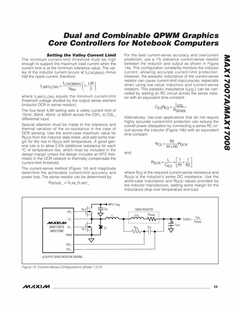
Setting the Valley Current LimitThe minimum current-limit threshold must be highenough to support the maximum load current when thecurrent limit is at the minimum tolerance value. The val-ley of the inductor current occurs at ILOAD(MAX) minushalf the ripple current; therefore:
where ILIMIT(LOW) equals the minimum current-limitthreshold voltage divided by the output sense element(inductor DCR or sense resistor).
The four-level ILIM setting sets a valley current limit of15mV, 30mV, 45mV, or 60mV across the CSH_ to CSL_differential input.
Special attention must be made to the tolerance andthermal variation of the on-resistance in the case ofDCR sensing. Use the worst-case maximum value forRDCR from the inductor data sheet, and add some mar-gin for the rise in RDCR with temperature. A good gen-eral rule is to allow 0.5% additional resistance for each°C of temperature rise, which must be included in thedesign margin unless the design includes an NTC ther-mistor in the DCR network to thermally compensate thecurrent-limit threshold.
The current-sense method (Figure 14) and magnitudedetermine the achievable current-limit accuracy andpower loss. The sense resistor can be determined by:
RSENSE_ = VLIM_/ILIMIT_
For the best current-sense accuracy and overcurrentprotection, use a 1% tolerance current-sense resistorbetween the inductor and output as shown in Figure14a. This configuration constantly monitors the inductorcurrent, allowing accurate current-limit protection.However, the parasitic inductance of the current-senseresistor can cause current-limit inaccuracies, especiallywhen using low-value inductors and current-senseresistors. This parasitic inductance (LESL) can be can-celled by adding an RC circuit across the sense resis-tor with an equivalent time constant:
Alternatively, low-cost applications that do not requirehighly accurate current-limit protection can reduce theoverall power dissipation by connecting a series RC cir-cuit across the inductor (Figure 14b) with an equivalenttime constant:
and:
where RCS is the required current-sense resistance andRDCR is the inductor’s series DC resistance. Use theworst-case inductance and RDCR values provided bythe inductor manufacturer, adding some margin for theinductance drop over temperature and load.
RL
C R RDCREQ
= × +⎡⎣⎢
⎤⎦⎥
11
12
RR
R RRCS DCR=
+2
1 2
C RL
REQ EQESL
SENSE=
II
NLIR
LIMIT LOWLOAD MAX
PH( )
( )> ⎛⎝⎜
⎞⎠⎟
12
-
MA
X1
70
07
A/M
AX
17
00
8
Dual and Combinable QPWM GraphicsCore Controllers for Notebook Computers
______________________________________________________________________________________ 29
SENSE RESISTOR
L
MAX17007AMAX17008
COUT
INPUT (VIN)
CIN
CSL_
CSH_
PGND
DL_
DH_
LX_
CEQREQ
NH
NLDL
LESL RSENSE
CEQREQ = LESL
RSENSE
a) OUTPUT SERIES RESISTOR SENSING
Figure 14. Current-Sense Configurations (Sheet 1 of 2)
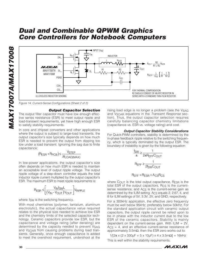
MA
X1
70
07
A/M
AX
17
00
8
Output Capacitor SelectionThe output filter capacitor must have low enough effec-tive series resistance (ESR) to meet output ripple andload-transient requirements, yet have high enough ESRto satisfy stability requirements.
In core and chipset converters and other applicationswhere the output is subject to large-load transients, theoutput capacitor’s size typically depends on how muchESR is needed to prevent the output from dipping toolow under a load transient. Ignoring the sag due to finitecapacitance:
In low-power applications, the output capacitor’s sizeoften depends on how much ESR is needed to maintainan acceptable level of output ripple voltage. The outputripple voltage of a step-down controller equals the totalinductor ripple current multiplied by the output capacitor’sESR. The maximum ESR to meet ripple requirements is:
where fSW is the switching frequency.
With most chemistries (polymer, tantalum, aluminumelectrolytic), the actual capacitance value requiredrelates to the physical size needed to achieve low ESRand the chemistry limits of the selected capacitor tech-nology. Ceramic capacitors provide low ESR, but thecapacitance and voltage rating (after derating) aredetermined by the capacity needed to prevent VSAGand VSOAR from causing problems during load tran-sients. Generally, once enough capacitance is addedto meet the overshoot requirement, undershoot at the
rising load edge is no longer a problem (see the VSAGand VSOAR equations in the Transient Response sec-tion). Thus, the output capacitor selection requirescarefully balancing capacitor chemistry limitations(capacitance vs. ESR vs. voltage rating) and cost.
Output Capacitor Stability ConsiderationsFor Quick-PWM controllers, stability is determined by thein-phase feedback ripple relative to the switching frequen-cy, which is typically dominated by the output ESR. Theboundary of instability is given by the following equation:
where COUT is the total output capacitance, RESR is thetotal ESR of the output capacitors, RCS is the current-sense resistance, and ACS is the current-sense gain asdetermined by the ILIM setting. ACS equals 2, 2.67, 4, and8 for ILIM settings of 5V, 3.3V, 2V, and GND, respectively.
For a 300kHz application, the effective zero frequencymust be well below 95kHz, preferably below 50kHz. Forthe standard application circuit with ceramic outputcapacitors, the output ripple cannot be relied upon tobe in phase with the inductor current due to the lowESR of the ceramic capacitors. Stability is mainlydependent on the current-sense gain. With ILIM = 2V,ACS = 4, and an effective current-sense resistance ofapproximately 3.5mΩ, then the ESR zero works out to:
1/[2π x (2 x 330μF + 5 x 10μF) x 4 x 3.5mΩ] = 16kHz
This is well within the stability requirements.
R R A REFF ESR CS CS= +
Rf CEFFSW OUT
≥ 12
fR C
SW
EFF OUTπ π≥ 1
2
RV f L
V V VVESR
IN SW
IN OUT OUTRIPPLE≤ ( )
⎡
⎣⎢⎢
⎤
⎦⎥⎥-
R RV
IESR PCBSTEP
LOAD MAX+( ) ≤
Δ ( )
Dual and Combinable QPWM GraphicsCore Controllers for Notebook Computers
30 ______________________________________________________________________________________
MAX17007AMAX17008
COUT
INPUT (VIN)
CIN
b) LOSSLESS INDUCTOR SENSING
FOR THERMAL COMPENSATION:R2 SHOULD CONSIST OF AN NTC RESISTOR INSERIES WITH A STANDARD THIN-FILM RESISTOR.
CSL_
CSH_
PGND
DL_
DH_
LX_
CEQ
R1 R2
NH
NLDL
L
INDUCTOR
RDCRRCS = R2 RDCR R1 + R2
RDCR = L [ 1 + 1 ]
CEQ R1 R2
Figure 14. Current-Sense Configurations (Sheet 2 of 2)
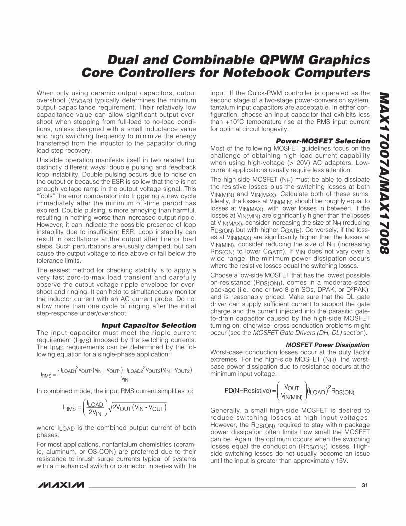
When only using ceramic output capacitors, outputovershoot (VSOAR) typically determines the minimumoutput capacitance requirement. Their relatively lowcapacitance value can allow significant output over-shoot when stepping from full-load to no-load condi-tions, unless designed with a small inductance valueand high switching frequency to minimize the energytransferred from the inductor to the capacitor duringload-step recovery.
Unstable operation manifests itself in two related butdistinctly different ways: double pulsing and feedbackloop instability. Double pulsing occurs due to noise onthe output or because the ESR is so low that there is notenough voltage ramp in the output voltage signal. This“fools” the error comparator into triggering a new cycleimmediately after the minimum off-time period hasexpired. Double pulsing is more annoying than harmful,resulting in nothing worse than increased output ripple.However, it can indicate the possible presence of loopinstability due to insufficient ESR. Loop instability canresult in oscillations at the output after line or loadsteps. Such perturbations are usually damped, but cancause the output voltage to rise above or fall below thetolerance limits.
The easiest method for checking stability is to apply avery fast zero-to-max load transient and carefullyobserve the output voltage ripple envelope for over-shoot and ringing. It can help to simultaneously monitorthe inductor current with an AC current probe. Do notallow more than one cycle of ringing after the initialstep-response under/overshoot.
Input Capacitor SelectionThe input capacitor must meet the ripple currentrequirement (IRMS) imposed by the switching currents.The IRMS requirements can be determined by the fol-lowing equation for a single-phase application:
In combined mode, the input RMS current simplifies to:
where ILOAD is the combined output current of bothphases.
For most applications, nontantalum chemistries (ceram-ic, aluminum, or OS-CON) are preferred due to theirresistance to inrush surge currents typical of systemswith a mechanical switch or connector in series with the
input. If the Quick-PWM controller is operated as thesecond stage of a two-stage power-conversion system,tantalum input capacitors are acceptable. In either con-figuration, choose an input capacitor that exhibits lessthan +10°C temperature rise at the RMS input currentfor optimal circuit longevity.
Power-MOSFET SelectionMost of the following MOSFET guidelines focus on thechallenge of obtaining high load-current capabilitywhen using high-voltage (> 20V) AC adapters. Low-current applications usually require less attention.
The high-side MOSFET (NH) must be able to dissipatethe resistive losses plus the switching losses at bothVIN(MIN) and VIN(MAX). Calculate both of these sums.Ideally, the losses at VIN(MIN) should be roughly equal tolosses at VIN(MAX), with lower losses in between. If thelosses at VIN(MIN) are significantly higher than the lossesat VIN(MAX), consider increasing the size of NH (reducingRDS(ON) but with higher CGATE). Conversely, if the loss-es at VIN(MAX) are significantly higher than the losses atVIN(MIN), consider reducing the size of NH (increasingRDS(ON) to lower CGATE). If VIN does not vary over awide range, the minimum power dissipation occurswhere the resistive losses equal the switching losses.
Choose a low-side MOSFET that has the lowest possibleon-resistance (RDS(ON)), comes in a moderate-sizedpackage (i.e., one or two 8-pin SOs, DPAK, or D2PAK),and is reasonably priced. Make sure that the DL gatedriver can supply sufficient current to support the gatecharge and the current injected into the parasitic gate-to-drain capacitor caused by the high-side MOSFETturning on; otherwise, cross-conduction problems mightoccur (see the MOSFET Gate Drivers (DH, DL) section).
MOSFET Power DissipationWorst-case conduction losses occur at the duty factorextremes. For the high-side MOSFET (NH), the worst-case power dissipation due to resistance occurs at theminimum input voltage:
Generally, a small high-side MOSFET is desired toreduce switching losses at high input voltages.However, the RDS(ON) required to stay within packagepower dissipation often limits how small the MOSFETcan be. Again, the optimum occurs when the switchinglosses equal the conduction (RDS(ON)) losses. High-side switching losses do not usually become an issueuntil the input is greater than approximately 15V.
PD NH sistiveV
VI ROUT
IN MINLOAD DS ON( Re )
( )( )=
⎛
⎝⎜
⎞
⎠⎟ ( )2
II
VVRMS
LOAD
INOUT=
⎛⎝⎜
⎞⎠⎟
( )2
2 V - VIN OUT
II V V V I V V V
VRMSLOAD OUT IN OUT LOAD OUT IN OUT
IN=
−( ) + −( )12
1 1 22
2 2
MA
X1
70
07
A/M
AX
17
00
8
Dual and Combinable QPWM GraphicsCore Controllers for Notebook Computers
______________________________________________________________________________________ 31
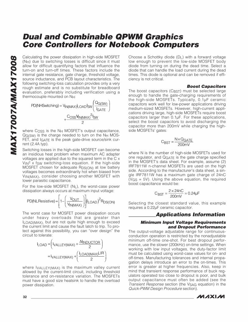
MA
X1
70
07
A/M
AX
17
00
8
Dual and Combinable QPWM GraphicsCore Controllers for Notebook Computers
32 ______________________________________________________________________________________
Calculating the power dissipation in high-side MOSFET(NH) due to switching losses is difficult since it mustallow for difficult quantifying factors that influence theturn-on and turn-off times. These factors include theinternal gate resistance, gate charge, threshold voltage,source inductance, and PCB layout characteristics. Thefollowing switching-loss calculation provides only a veryrough estimate and is no substitute for breadboardevaluation, preferably including verification using athermocouple mounted on NH:
where COSS is the NH MOSFET’s output capacitance,QG(SW) is the charge needed to turn on the NH MOS-FET, and IGATE is the peak gate-drive source/sink cur-rent (2.4A typ).
Switching losses in the high-side MOSFET can becomean insidious heat problem when maximum AC adaptervoltages are applied due to the squared term in the C xVIN2 x fSW switching-loss equation. If the high-sideMOSFET chosen for adequate RDS(ON) at low batteryvoltages becomes extraordinarily hot when biased fromVIN(MAX), consider choosing another MOSFET withlower parasitic capacitance.
For the low-side MOSFET (NL), the worst-case powerdissipation always occurs at maximum input voltage:
The worst case for MOSFET power dissipation occursunder heavy overloads that are greater thanILOAD(MAX), but are not quite high enough to exceedthe current limit and cause the fault latch to trip. To pro-tect against this possibility, you can “over design” thecircuit to tolerate:
where IVALLEY(MAX) is the maximum valley currentallowed by the current-limit circuit, including thresholdtolerance and on-resistance variation. The MOSFETsmust have a good size heatsink to handle the overloadpower dissipation.
Choose a Schottky diode (DL) with a forward voltagelow enough to prevent the low-side MOSFET bodydiode from turning on during the dead time. Select adiode that can handle the load current during the deadtimes. This diode is optional and can be removed if effi-ciency is not critical.
Boost CapacitorsThe boost capacitors (CBST) must be selected largeenough to handle the gate-charging requirements ofthe high-side MOSFETs. Typically, 0.1μF ceramiccapacitors work well for low-power applications drivingmedium-sized MOSFETs. However, high-current appli-cations driving large, high-side MOSFETs require boostcapacitors larger than 0.1μF. For these applications,select the boost capacitors to avoid discharging thecapacitor more than 200mV while charging the high-side MOSFETs’ gates:
where N is the number of high-side MOSFETs used forone regulator, and QGATE is the gate charge specifiedin the MOSFET’s data sheet. For example, assume (2)IRF7811W n-channel MOSFETs are used on the highside. According to the manufacturer’s data sheet, a sin-gle IRF7811W has a maximum gate charge of 24nC(VGS = 5V). Using the above equation, the requiredboost capacitance would be:
Selecting the closest standard value, this examplerequires a 0.22μF ceramic capacitor.
Applications InformationMinimum Input Voltage Requirements
and Dropout PerformanceThe output-voltage adjustable range for continuous-conduction operation is restricted by the nonadjustableminimum off-time one-shot. For best dropout perfor-mance, use the slower (200kHz) on-time settings. Whenworking with low input voltages, the duty-factor limitmust be calculated using worst-case values for on- andoff-times. Manufacturing tolerances and internal propa-gation delays introduce an error to the on-times. Thiserror is greater at higher frequencies. Also, keep inmind that transient response performance of buck reg-ulators operated too close to dropout is poor, and bulkoutput capacitance must often be added (see theTransient Response section (the VSAG equation) in theQuick-PWM Design Procedure section).
CnC
mVμFBST = × =2 24
2000 24.
CN Q
mVBSTGATE= ×
200
I II
II LIR
LOAD VALLEY MAXINDUCTOR
VALLEY MAXLOAD MAX
= +⎛⎝⎜
⎞⎠⎟
= +⎛
⎝⎜⎞
⎠⎟
( )
( )( )
Δ2
2
PD NL sistiveV
VI ROUT
IN MAXLOAD DS ON( Re )
( )( )= −
⎛
⎝⎜
⎞
⎠⎟
⎡
⎣⎢⎢
⎤
⎦⎥⎥
( )1 2
PD NHSwitching V I fQ
IIN MAX LOAD SWG SW
GATE( ) ( )
( )=⎛⎛
⎝⎜
⎞
⎠⎟
+COSSVV fIN MAX SW( )
2
2
In a single-phase configuration, the absolute point ofdropout is when the inductor current ramps down dur-ing the minimum off-time (ΔIDOWN) as much as it rampsup during the on-time (ΔIUP). The ratio h = ΔIUP/ΔIDOWN is an indicator of the ability to slew the inductorcurrent higher in response to increased load and mustalways be greater than 1. As h approaches 1—theabsolute minimum dropout point—the inductor currentcannot increase as much during each switching cycle,and VSAG greatly increases unless additional outputcapacitance is used. A reasonable minimum value for his 1.5, but adjusting this up or down allows trade-offsbetween VSAG, output capacitance, and minimumoperating voltage. For a given value of h, the minimumoperating voltage can be calculated as:
where VCHG is the parasitic voltage drop in the chargepath (see the On-Time One-Shot section), and tOFF(MIN)is from the Electrical Characteristics table. The absoluteminimum input voltage is calculated with h = 1.
If the calculated VIN(MIN) is greater than the required min-imum input voltage, then reduce the operating frequencyor add output capacitance to obtain an acceptable VSAG.If operation near dropout is anticipated, calculate VSAG tobe sure of adequate transient response.
Dropout Design Example:
VOUT = 1.5V
fSW = 300kHz
tOFF(MIN) = 250ns
VCHG = 150mV (10A load)
h = 1.5:
Calculating again with h = 1 gives the absolute limit ofdropout:
Therefore, VIN must be greater than 1.78V, even withvery large output capacitance, and a practical input volt-age with reasonable output capacitance would be 2.0V.
PCB Layout GuidelinesCareful PCB layout is critical to achieve low switchinglosses and clean, stable operation. The switchingpower stage requires particular attention. If possible,mount all the power components on the top side of theboard with their ground terminals flush against oneanother. Follow these guidelines for good PCB layout:
• Keep the high-current paths short, especially at theground terminals. This is essential for stable, jitter-free operation.
• Connect all analog grounds to a separate solid cop-per plane, which connects to the GND pin of theQuick-PWM controller. This includes the VCCbypass capacitor, REF bypass capacitors, REFIN1components, and feedback compensation/dividers.
• Keep the power traces and load connections short.This is essential for high efficiency. The use of thickcopper PCBs (2oz vs. 1oz) can enhance full-loadefficiency by 1% or more. Correctly routing PCBtraces is a difficult task that must be approached interms of fractions of centimeters, where a single mil-liohm of excess trace resistance causes a measur-able efficiency penalty.
• Keep the high current, gate-driver traces (DL, DH,LX, and BST) short and wide to minimize traceresistance and inductance. This is essential forhigh-power MOSFETs that require low-impedancegate drivers to avoid shoot-through currents.
• When trade-offs in trace lengths must be made, it ispreferable to allow the inductor charging path to bemade longer than the discharge path. For example,it is better to allow some extra distance between theinput capacitors and the high-side MOSFET than toallow distance between the inductor and the low-side MOSFET or between the inductor and the out-put filter capacitor.
• Route high-speed switching nodes away from sensi-tive analog areas (REF, REFIN1, FB2, CSH, and CSL).
Layout Procedure1) Place the power components first, with ground ter-
minals adjacent (low-side MOSFET source, CIN,COUT, and anode of the low-side Schottky). If possi-ble, make all these connections on the top layerwith wide, copper-filled areas.
2) Mount the controller IC adjacent to the low-sideMOSFET. The DL gate traces must be short andwide (50 mils to 100 mils wide if the MOSFET is 1infrom the controller IC).
VV mV
μs kHzIN MIN( ).
( . . )= +
× ×⎡⎣⎢
1 5 1501 0 25 1 0 300-
⎤⎤⎦⎥ = 1 78. V
VV mV
μs kHzIN MIN( ).
( . . )= +
× ×⎡⎣⎢
1 5 1501 0 25 1 5 300-
⎤⎤⎦⎥ = 1 86. V
VV V
h t fIN MIN
OUT CHG
OFF MIN SW( )
( )=
×( )⎛
⎝⎜⎜
⎞
⎠⎟
+
-1 ⎟⎟
MA
X1
70
07
A/M
AX
17
00
8
Dual and Combinable QPWM GraphicsCore Controllers for Notebook Computers
______________________________________________________________________________________ 33
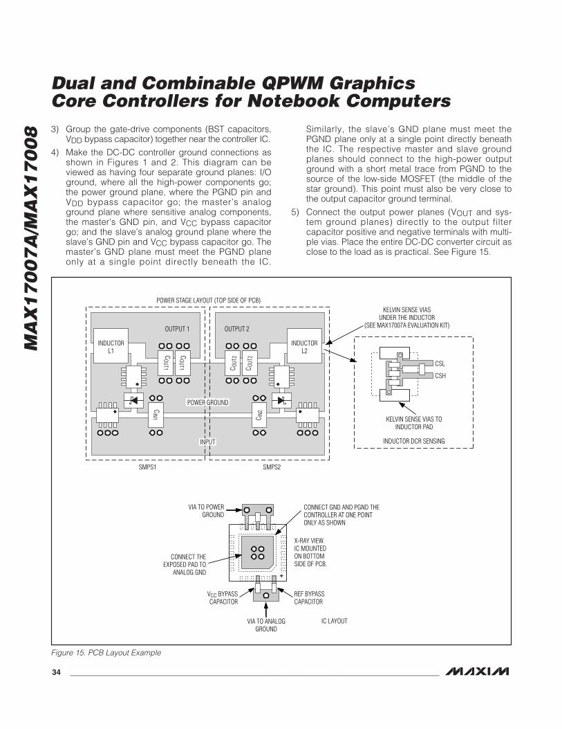
MA
X1
70
07
A/M
AX
17
00
8 3) Group the gate-drive components (BST capacitors,VDD bypass capacitor) together near the controller IC.
4) Make the DC-DC controller ground connections asshown in Figures 1 and 2. This diagram can beviewed as having four separate ground planes: I/Oground, where all the high-power components go;the power ground plane, where the PGND pin andVDD bypass capacitor go; the master’s analogground plane where sensitive analog components,the master’s GND pin, and VCC bypass capacitorgo; and the slave’s analog ground plane where theslave’s GND pin and VCC bypass capacitor go. Themaster’s GND plane must meet the PGND planeonly at a single point directly beneath the IC.
Similarly, the slave’s GND plane must meet thePGND plane only at a single point directly beneaththe IC. The respective master and slave groundplanes should connect to the high-power outputground with a short metal trace from PGND to thesource of the low-side MOSFET (the middle of thestar ground). This point must also be very close tothe output capacitor ground terminal.
5) Connect the output power planes (VOUT and sys-tem ground planes) directly to the output filtercapacitor positive and negative terminals with multi-ple vias. Place the entire DC-DC converter circuit asclose to the load as is practical. See Figure 15.
Dual and Combinable QPWM GraphicsCore Controllers for Notebook Computers
34 ______________________________________________________________________________________
OUTPUT 1
SMPS1
COUT1
COUT1 C O
UT2
C OUT
2
CIN1 C I
N2
SMPS2
OUTPUT 2
KELVIN SENSE VIASUNDER THE INDUCTOR
(SEE MAX17007A EVALUATION KIT)
VIA TO POWERGROUND
VCC BYPASSCAPACITOR
REF BYPASSCAPACITOR
X-RAY VIEW.IC MOUNTEDON BOTTOMSIDE OF PCB.
IC LAYOUT
CONNECT GND AND PGND THECONTROLLER AT ONE POINTONLY AS SHOWN
CONNECT THEEXPOSED PAD TO
ANALOG GND
VIA TO ANALOGGROUND
POWER STAGE LAYOUT (TOP SIDE OF PCB)
INDUCTORL1
INDUCTORL2
INPUT
POWER GROUND
+
INDUCTOR DCR SENSING
KELVIN SENSE VIAS TOINDUCTOR PAD
CSL
CSH
Figure 15. PCB Layout Example
MA
X1
70
07
A/M
AX
17
00
8
Dual and Combinable QPWM GraphicsCore Controllers for Notebook Computers
______________________________________________________________________________________ 35
PACKAGE TYPE PACKAGE CODE DOCUMENT NO.
28 TQFN T2844-1 21-0139
Chip InformationTRANSISTOR COUNT: 13,103
PROCESS: BiCMOS
Package InformationFor the latest package outline information and land patterns, goto www.maxim-ic.com/packages.
MA
X1
70
07
A/M
AX
17
00
8
Dual and Combinable QPWM GraphicsCore Controllers for Notebook Computers
Maxim cannot assume responsibility for use of any circuitry other than circuitry entirely embodied in a Maxim product. No circuit patent licenses areimplied. Maxim reserves the right to change the circuitry and specifications without notice at any time.
36 ____________________Maxim Integrated Products, 120 San Gabriel Drive, Sunnyvale, CA 94086 408-737-7600
© 2008 Maxim Integrated Products is a registered trademark of Maxim Integrated Products, Inc.
Revision History
REVISION NUMBER
REVISION DATE
DESCRIPTIONPAGES
CHANGED
0 2/08 Initial release —
1 9/08 Changed MAX17007 to MAX17007A, changed EC table, and corrected typos 1–8, 11, 12, 13, 16,
18, 24, 25
2 10/08 Released the MAX17008. Updated the EC table. 1, 3, 6