Dual current limited overvoltage protected digital termination · PCLT-2A Description Doc ID 11821...
20
This is information on a product in full production. March 2012 Doc ID 11821 Rev 2 1/20 20 PCLT-2A Dual current limited overvoltage protected digital termination Datasheet − production data Features ■ 2 channel topology: low side input with common ground ■ Wide range input DC voltage: – V I = - 0.3 to 30 V with R I = 0 Ω – V I = - 30 to 35 V with R I = 750 Ω ■ Current limiter: – 3 to 7.5 mA programmable reference – I LIM = 6.1 mA to 8.8 mA with R REF = 10 kΩ – I LIM = 2.8 mA to 4.3 mA with R REF = 22 kΩ – Narrow limiter spread: < 17% – Temperature compensated operation ■ Output drive: – No output activation below 2 mA input – 1.5 mA minimum output activating current in opto-coupler mode – Programmable CMOS output mode option (V MOD > 2.9 V) ■ LED drive for sensor status: 4.4 mA typical with R REF = 10 kΩ ■ Input protection (R I = 750 Ω C IN = 22 nF) ■ IEC 61000-4-2 ESD, Level 4 – In contact, ± 8 kV; in air, ± 15 kV – Criteria B: temporary disruption ■ IEC 61000-4-5 voltage surge, Level 3 – ± 500 V with 42 Ω series resistor in differential mode – Criteria B: temporary disruption ■ IEC 61000-4-4 transient burst immunity – ± 4 kV peak voltage; 5 kHz repetitive rate – Criteria A: fully functional ■ IEC 61000-4-6 conducted RFI – 10 V RMS – Criteria A: fully functional ■ Input protection against -30 V reverse polarity ■ Ambient temperature: -25 to 85 °C Benefits ■ Enable input to meet type1, 2 and 3 characteristics of IEC 61131-2 standard ■ Compatible operation with 2 and 3 wires proximity sensor according EN60947-5-2 standard ■ Flexible configuration driving either opto- coupler, or CMOS bus controller input, or 12 V AS-Interface network ■ Reduced overall dissipation ■ Enhanced functional reliability ■ Compact with high integration ■ Surface mount package for highly automated assembly ■ Insensitive to the on-state sensor impedance Applications ■ Type 1, 2 and 3 logic input termination for industrial automation ■ AS-Interface bus input termination ■ I/O termination in programmable logic controller ■ Proximity detector interface ■ Decentralized input / output modules TSSOP14 Exposed pad www.st.com
Transcript of Dual current limited overvoltage protected digital termination · PCLT-2A Description Doc ID 11821...
This is information on a product in full production.
March 2012 Doc ID 11821 Rev 2 1/20
20
PCLT-2A
Dual current limited overvoltage protected digital termination
Datasheet − production data
Features■ 2 channel topology: low side input with
common ground
■ Wide range input DC voltage:– VI = - 0.3 to 30 V with RI = 0 Ω– VI = - 30 to 35 V with RI = 750 Ω
■ Current limiter:– 3 to 7.5 mA programmable reference– ILIM = 6.1 mA to 8.8 mA with RREF = 10 kΩ– ILIM = 2.8 mA to 4.3 mA with RREF = 22 kΩ– Narrow limiter spread: < 17%– Temperature compensated operation
■ Output drive:– No output activation below 2 mA input – 1.5 mA minimum output activating current
in opto-coupler mode– Programmable CMOS output mode option
(VMOD > 2.9 V)
■ LED drive for sensor status: 4.4 mA typical with RREF = 10 kΩ
■ Input protection (RI = 750 Ω CIN = 22 nF)
■ IEC 61000-4-2 ESD, Level 4– In contact, ± 8 kV; in air, ± 15 kV– Criteria B: temporary disruption
■ IEC 61000-4-5 voltage surge, Level 3– ± 500 V with 42 Ω series resistor in
differential mode– Criteria B: temporary disruption
■ IEC 61000-4-4 transient burst immunity– ± 4 kV peak voltage; 5 kHz repetitive rate– Criteria A: fully functional
■ IEC 61000-4-6 conducted RFI– 10 VRMS– Criteria A: fully functional
■ Input protection against -30 V reverse polarity
■ Ambient temperature: -25 to 85 °C
Benefits
■ Enable input to meet type1, 2 and 3 characteristics of IEC 61131-2 standard
■ Compatible operation with 2 and 3 wires proximity sensor according EN60947-5-2 standard
■ Flexible configuration driving either opto- coupler, or CMOS bus controller input, or 12 V AS-Interface network
■ Reduced overall dissipation
■ Enhanced functional reliability
■ Compact with high integration
■ Surface mount package for highly automated assembly
■ Insensitive to the on-state sensor impedance
Applications■ Type 1, 2 and 3 logic input termination for
industrial automation
■ AS-Interface bus input termination
■ I/O termination in programmable logic controller
■ Proximity detector interface
■ Decentralized input / output modules
TSSOP14Exposed pad
www.st.com
Contents PCLT-2A
2/20 Doc ID 11821 Rev 2
Contents
1 Description . . . . . . . . . . . . . . . . . . . . . . . . . . . . . . . . . . . . . . . . . . . . . . . . . 3
2 Characteristics . . . . . . . . . . . . . . . . . . . . . . . . . . . . . . . . . . . . . . . . . . . . . 3
2.1 IEC61000-4 standard compliance application diagrams . . . . . . . . . . . . . . 3
2.2 Functional characteristics . . . . . . . . . . . . . . . . . . . . . . . . . . . . . . . . . . . . . . 9
2.3 Functional description . . . . . . . . . . . . . . . . . . . . . . . . . . . . . . . . . . . . . . . 11
2.3.1 The VMOD pin . . . . . . . . . . . . . . . . . . . . . . . . . . . . . . . . . . . . . . . . . . . . 11
2.3.2 OFF state . . . . . . . . . . . . . . . . . . . . . . . . . . . . . . . . . . . . . . . . . . . . . . . . 11
2.3.3 ON state . . . . . . . . . . . . . . . . . . . . . . . . . . . . . . . . . . . . . . . . . . . . . . . . . 12
3 Surge voltage test circuit . . . . . . . . . . . . . . . . . . . . . . . . . . . . . . . . . . . . 13
4 Input reverse polarity robustness . . . . . . . . . . . . . . . . . . . . . . . . . . . . . 14
5 Programming of the PCLT-2A according to input type requirement . 15
6 Unisolated AS-Interface bus application diagram . . . . . . . . . . . . . . . . 16
6.1 AS-Interface bus application overview . . . . . . . . . . . . . . . . . . . . . . . . . . . 16
6.2 Isolation of the sensor section and the supply from data/supply bus . . . . 16
6.3 Unisolated connection of the PCLT with AS-Interface controller . . . . . . . 17
7 Package information . . . . . . . . . . . . . . . . . . . . . . . . . . . . . . . . . . . . . . . . 18
8 Ordering information scheme . . . . . . . . . . . . . . . . . . . . . . . . . . . . . . . . 19
9 Ordering information . . . . . . . . . . . . . . . . . . . . . . . . . . . . . . . . . . . . . . . 19
10 Revision history . . . . . . . . . . . . . . . . . . . . . . . . . . . . . . . . . . . . . . . . . . . 19
PCLT-2A Description
Doc ID 11821 Rev 2 3/20
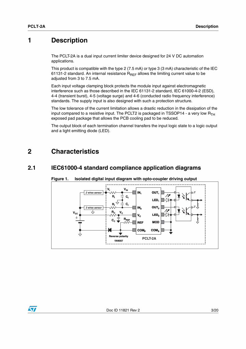
1 Description
The PCLT-2A is a dual input current limiter device designed for 24 V DC automation applications.
This product is compatible with the type 2 (7.5 mA) or type 3 (3 mA) characteristic of the IEC 61131-2 standard. An internal resistance RREF allows the limiting current value to be adjusted from 3 to 7.5 mA.
Each input voltage clamping block protects the module input against electromagnetic interference such as those described in the IEC 61131-2 standard, IEC 61000-4-2 (ESD), 4-4 (transient burst), 4-5 (voltage surge) and 4-6 (conducted radio frequency interference) standards. The supply input is also designed with such a protection structure.
The low tolerance of the current limitation allows a drastic reduction in the dissipation of the input compared to a resistive input. The PCLT2 is packaged in TSSOP14 - a very low RTH exposed pad package that allows the PCB cooling pad to be reduced.
The output block of each termination channel transfers the input logic state to a logic output and a light emitting diode (LED).
2 Characteristics
2.1 IEC61000-4 standard compliance application diagrams
Figure 1. Isolated digital input diagram with opto-coupler driving output
3 wires sensor
2 wires sensor
RI
RI
RC
VINVI
VCC VC
RREF
Reverse polarity
1N4007
CI
CI
CC
IN1
COMP
IN2
VC
REF
OUT1
OUT2
COMS
LED2
LED1
MOD
PCLT-2A
3 wires sensor
2 wires sensor
RI
RI
RC
VINVI
VCC VC
RREF
Reverse polarity
1N4007
CI
CI
CC
IN1
COMP
IN2
VC
REF
OUT1
OUT2
COMS
LED2
LED1
MOD
IN1
COMP
IN2
VC
REF
OUT1
OUT2
COMS
LED2
LED1
MOD
Characteristics PCLT-2A
4/20 Doc ID 11821 Rev 2
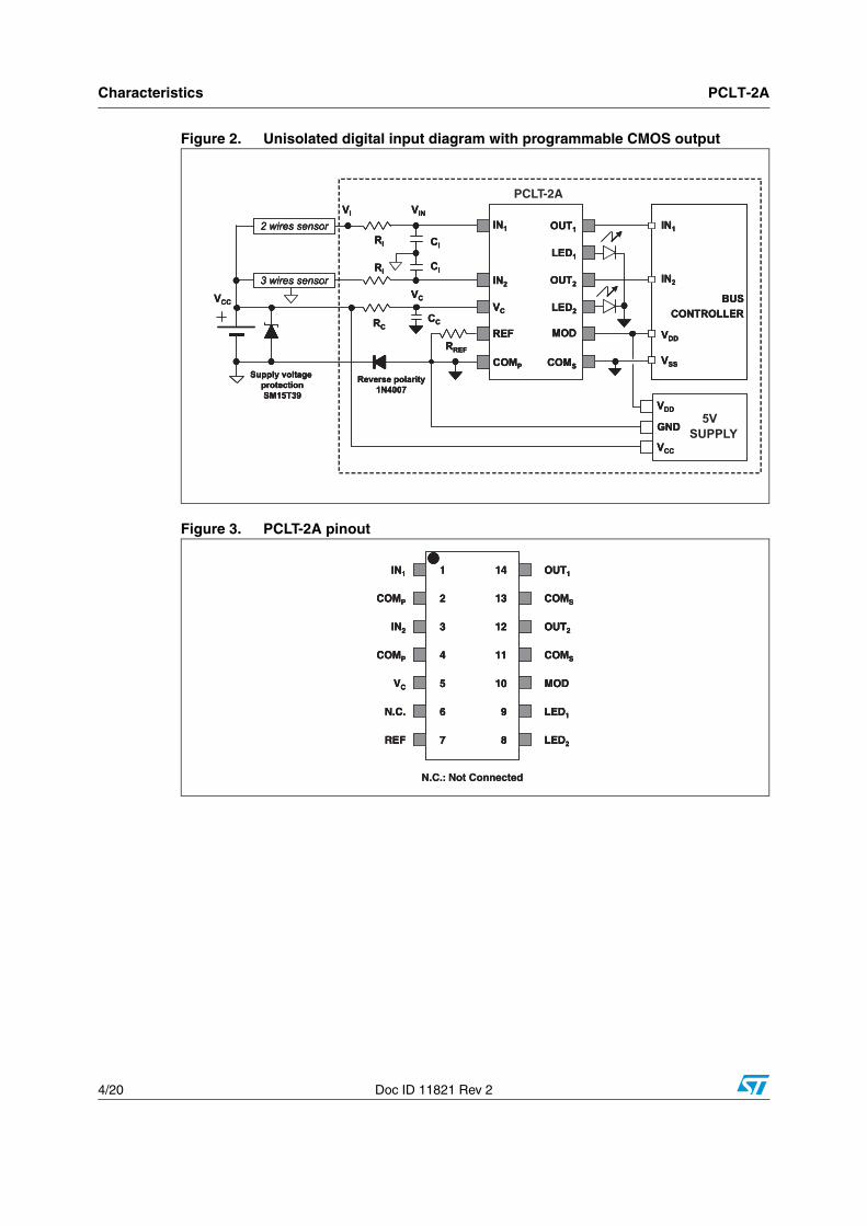
Figure 2. Unisolated digital input diagram with programmable CMOS output
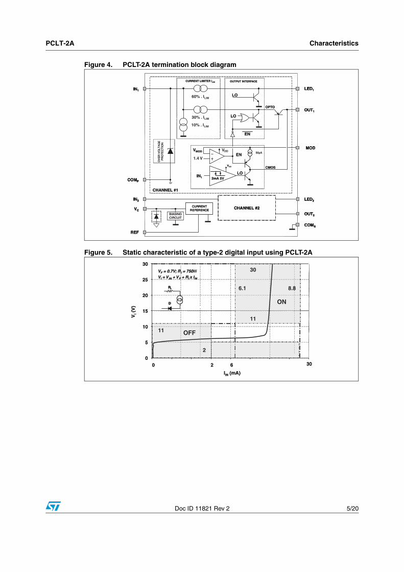
Figure 3. PCLT-2A pinout
VSS
VDD
IN2
IN1
BUS
CONTROLLER
VDD
GND
VCC
Supply voltage
protection
SM15T39
3 wires sensor
2 wires sensor
RI
RI
RC
VIN
VI
VCC
VC
RREF
CI
CI
CC
Reverse polarity
1N4007
IN1
COMP
IN2
OUT1
OUT2
COMS
LED2
LED1
VC
REF MOD
VSS
VDD
IN2
IN1
BUS
CONTROLLER
VDD
GND
VCC
VSS
VDD
IN2
IN1
BUS
CONTROLLER
VDD
GND
VCC
5V
SUPPLY
Supply voltage
protection
SM15T39
3 wires sensor
2 wires sensor
RI
RI
RC
VIN
VI
VCC
VC
RREF
CI
CI
CC
Reverse polarity
1N4007
Supply voltage
protection
SM15T39
3 wires sensor
2 wires sensor
RI
RI
RC
VIN
VI
VCC
VC
RREF
CI
CI
CC
Reverse polarity
1N4007
IN1
COMP
IN2
OUT1
OUT2
COMS
LED2
LED1
VC
REF MOD
IN1
COMP
IN2
OUT1
OUT2
COMS
LED2
LED1
VC
REF MOD
PCLT-2A
OUT1
OUT2
MOD
LED1
COMS
COMS
LED2
1
2
3
4
5
6
7 8
9
10
11
12
13
14IN1
IN2
REF
VC
COMP
COMP
N.C.
N.C.: Not Connected
OUT1
OUT2
MOD
LED1
COMS
COMS
LED2
OUT1
OUT2
MOD
LED1
COMS
COMS
LED2
1
2
3
4
5
6
7 8
9
10
11
12
13
141
2
3
4
5
6
7 8
9
10
11
12
13
14IN1
IN2
REF
VC
COMP
COMP
N.C.
IN1
IN2
REF
VC
COMP
COMP
N.C.
N.C.: Not Connected
PCLT-2A Characteristics
Doc ID 11821 Rev 2 5/20
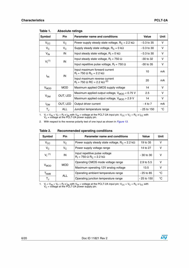
Figure 4. PCLT-2A termination block diagram
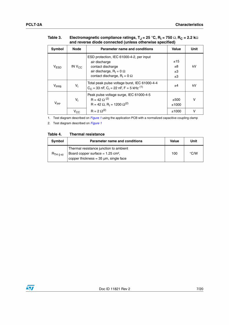
Figure 5. Static characteristic of a type-2 digital input using PCLT-2A
COMS
OUT1
LED1
OUT2
LED2
MOD
COMP
IN1
IN2
VC
REF
CURRENTREFERENCE
CHANNEL #2
CHANNEL #1
BIASINGCIRCUIT
CURRENT LIMITER ILIM
60% . ILIM
10% . ILIM
30% . ILIM
OV
ER
VO
LTA
GE
PR
OT
EC
TIO
N
OUTPUT INTERFACE
LO
OPTO
CMOS
IN1LO
VMODEN
LO
EN
50µA
VCC
2mA 5V
COMS
OUT1
LED1
OUT2
LED2
MOD
COMS
OUT1
LED1
OUT2
LED2
MOD
COMP
IN1
IN2
VC
REF
COMP
IN1
IN2
VC
REF
CURRENTREFERENCE
CURRENTREFERENCE
CHANNEL #2CHANNEL #2
CHANNEL #1
BIASINGCIRCUIT
CURRENT LIMITER ILIM
OV
ER
VO
LTA
GE
PR
OT
EC
TIO
N
OUTPUT INTERFACE
LO
OPTO
CMOS
IN1LO
VMOD
1.4 V
VDDEN
LO
EN
50µA
VCC
2mA 5V
VF = 0.7V; RI = 750WVI = VIN + VF + RI x IIN
VI(V
)
0
5
10
15
20
25
30
0 2 6
IIN (mA)
6.1 8.5
30
ON
OFF
11
RI
D
2
11
30
VF = 0.7V; RI = 750WVI = VIN + VF + RI x IIN
VI(V
)
0
5
10
15
20
25
30
0 2 6
IIN (mA)
6.1 8.8
30
ON
OFF
11
RI
D
RI
D
2
11
30
Characteristics PCLT-2A
6/20 Doc ID 11821 Rev 2
Table 1. Absolute ratings
Symbol Pin Parameter name and conditions Value Unit
VCC VC Power supply steady state voltage, RC = 2.2 kΩ - 0.3 to 35 V
VC VC Supply steady state voltage, RC = 0 kΩ - 0.3 to 30 V
VIN IN Input steady state voltage, RI = 0 kΩ - 0.3 to 30 V
VI(1)
1. VI = VIN + VF + RI x IIN with VIN = voltage at the PCLT-2A input pin; VCC = VC + RC x ICC with VC = voltage at the PCLT-2A power supply pin.
INInput steady state voltage, RI = 750 Ω -30 to 32 V
Input repetitive pulse voltage, RI = 750 Ω -30 to 35 V
IIN IN
Input maximum forward currentRI = 750 Ω RC = 2.2 kΩ
10 mA
Input maximum reverse currentRI = 750 Ω RC = 2.2 kΩ (2)
2. With respect to the reverse polarity test of one input as shown in Figure 13.
20 mA
VMOD MOD Maximum applied CMOS supply voltage 14 V
VOM OUT, LEDMaximum applied output voltage, VMOD < 0.75 V 2.5 V
Maximum applied output voltage, VMOD > 2.9 V 14 V
IOM OUT, LED Output driver current - 4 to 7 mA
TJ ALL Junction temperature range - 25 to 150 °C
Table 2. Recommended operating conditions
Symbol Pin Parameter name and conditions Value Unit
VCC VC Power supply steady state voltage, RC = 2.2 kΩ 19 to 35 V
VC VC Power supply voltage range 14 to 27 V
VI (1)
1. VI = VIN + VF + RI x IIN with VIN = voltage at the PCLT-2A input pin; VCC = VC + RC x ICC with VC = voltage at the PCLT-2A power supply pin.
INInput repetitive pulse voltage RI = 750 Ω RC = 2.2 kΩ - 30 to 30 V
VMOD MODOperating CMOS mode voltage range 2.9 to 5.5 V
Maximum operating 12V analog voltage 13.5 V
TAMBALL
Operating ambient temperature range - 25 to 85 °C
TJ Operating junction temperature range - 25 to 150 °C
PCLT-2A Characteristics
Doc ID 11821 Rev 2 7/20
)
Table 3. Electromagnetic compliance ratings, TJ = 25 °C, RI = 750 Ω, RC = 2.2 kΩ and reverse diode connected (unless otherwise specified)
Symbol Node Parameter name and conditions Value Unit
VESD IN VCC
ESD protection, IEC 61000-4-2, per inputair dischargecontact dischargeair discharge, RI = 0 Ωcontact discharge, RI = 0 Ω
±15
±8
±3±3
kV
VPPB VITotal peak pulse voltage burst, IEC 61000-4-4CC = 33 nF, CI = 22 nF, F = 5 kHz (1)
1. Test diagram described on Figure 1 using the application PCB with a normalized capacitive coupling clamp
±4 kV
VPP
VI
Peak pulse voltage surge, IEC 61000-4-5
R = 42 Ω (2)
R = 42 Ω, RI = 1200 Ω(2)
2. Test diagram described on Figure 1
±500
±1000
V
VCC R = 2 Ω(2) ±1000 V
Table 4. Thermal resistance
Symbol Parameter name and conditions Value Unit
RTH (j-a)
Thermal resistance junction to ambient
Board copper surface = 1.25 cm²,
copper thickness = 35 µm, single face
100 °C/W
Characteristics PCLT-2A
8/20 Doc ID 11821 Rev 2
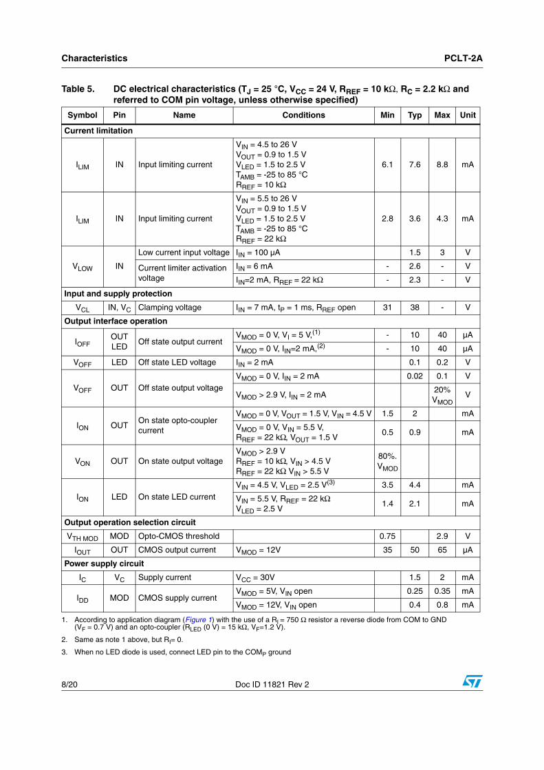
Table 5. DC electrical characteristics (TJ = 25 °C, VCC = 24 V, RREF = 10 kΩ, RC = 2.2 kΩ and referred to COM pin voltage, unless otherwise specified)
Symbol Pin Name Conditions Min Typ Max Unit
Current limitation
ILIM IN Input limiting current
VIN = 4.5 to 26 V VOUT = 0.9 to 1.5 V VLED = 1.5 to 2.5 V TAMB = -25 to 85 °CRREF = 10 kΩ
6.1 7.6 8.8 mA
ILIM IN Input limiting current
VIN = 5.5 to 26 V VOUT = 0.9 to 1.5 V VLED = 1.5 to 2.5 V TAMB = -25 to 85 °CRREF = 22 kΩ
2.8 3.6 4.3 mA
VLOW IN
Low current input voltage IIN = 100 µA 1.5 3 V
Current limiter activation voltage
IIN = 6 mA - 2.6 - V
IIN=2 mA, RREF = 22 kΩ - 2.3 - V
Input and supply protection
VCL IN, VC Clamping voltage IIN = 7 mA, tP = 1 ms, RREF open 31 38 - V
Output interface operation
IOFFOUT LED
Off state output currentVMOD = 0 V, VI = 5 V,(1) - 10 40 µA
VMOD = 0 V, IIN=2 mA,(2) - 10 40 µA
VOFF LED Off state LED voltage IIN = 2 mA 0.1 0.2 V
VOFF OUT Off state output voltageVMOD = 0 V, IIN = 2 mA 0.02 0.1 V
VMOD > 2.9 V, IIN = 2 mA20%VMOD
V
ION OUTOn state opto-coupler current
VMOD = 0 V, VOUT = 1.5 V, VIN = 4.5 V 1.5 2 mA
VMOD = 0 V, VIN = 5.5 V,RREF = 22 kΩ, VOUT = 1.5 V
0.5 0.9 mA
VON OUT On state output voltageVMOD > 2.9 V RREF = 10 kΩ, VIN > 4.5 V RREF = 22 kΩ VIN > 5.5 V
80%. VMOD
ION LED On state LED current
VIN = 4.5 V, VLED = 2.5 V(3) 3.5 4.4 mA
VIN = 5.5 V, RREF = 22 kΩ VLED = 2.5 V
1.4 2.1 mA
Output operation selection circuit
VTH MOD MOD Opto-CMOS threshold 0.75 2.9 V
IOUT OUT CMOS output current VMOD = 12V 35 50 65 µA
Power supply circuit
IC VC Supply current VCC = 30V 1.5 2 mA
IDD MOD CMOS supply currentVMOD = 5V, VIN open 0.25 0.35 mA
VMOD = 12V, VIN open 0.4 0.8 mA
1. According to application diagram (Figure 1) with the use of a RI = 750 Ω resistor a reverse diode from COM to GND(VF = 0.7 V) and an opto-coupler (RLED (0 V) = 15 kΩ, VF=1.2 V).
2. Same as note 1 above, but RI= 0.
3. When no LED diode is used, connect LED pin to the COMP ground
PCLT-2A Characteristics
Doc ID 11821 Rev 2 9/20
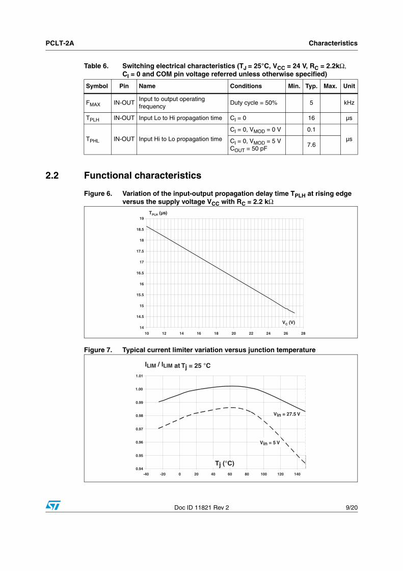
2.2 Functional characteristics
Figure 6. Variation of the input-output propagation delay time TPLH at rising edge versus the supply voltage VCC with RC = 2.2 kΩ
Figure 7. Typical current limiter variation versus junction temperature
Table 6. Switching electrical characteristics (TJ = 25°C, VCC = 24 V, RC = 2.2kΩ, CI = 0 and COM pin voltage referred unless otherwise specified)
Symbol Pin Name Conditions Min. Typ. Max. Unit
FMAX IN-OUTInput to output operating frequency
Duty cycle = 50% 5 kHz
TPLH IN-OUT Input Lo to Hi propagation time CI = 0 16 µs
TPHL IN-OUT Input Hi to Lo propagation time
CI = 0, VMOD = 0 V 0.1
µsCI = 0, VMOD = 5 VCOUT = 50 pF
7.6
14
14.5
15
15.5
16
16.5
17
17.5
18
18.5
19
10 12 14 16 18 20 22 24 26 28
TPLH (µs)
VC (V)
0.94
0.95
0.96
0.97
0.98
0.99
1.00
1.01
-40 -20 0 20 40 60 80 100 120 140
Tj (°C)
I / I at Tj = 25 °CLIM LIM
Vin = 5 V
Vin = 27.5 V
Characteristics PCLT-2A
10/20 Doc ID 11821 Rev 2
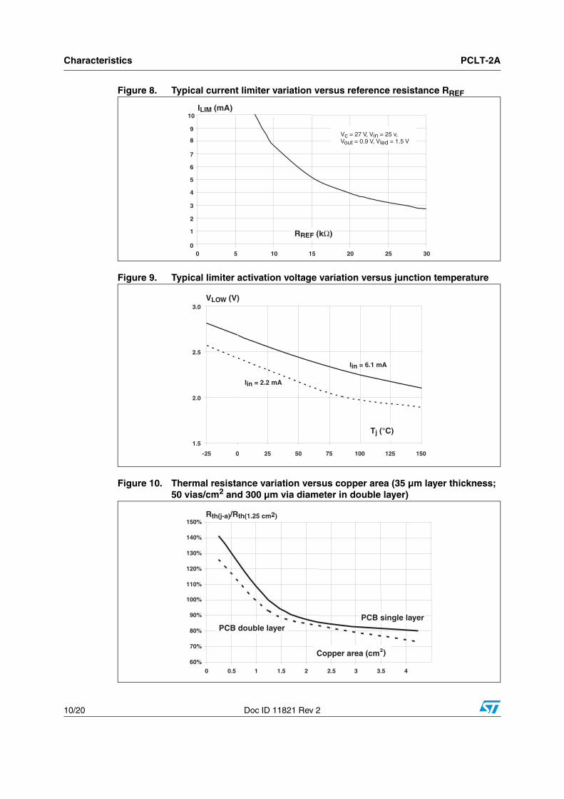
Figure 8. Typical current limiter variation versus reference resistance RREF
Figure 9. Typical limiter activation voltage variation versus junction temperature
Figure 10. Thermal resistance variation versus copper area (35 µm layer thickness; 50 vias/cm2 and 300 µm via diameter in double layer)
0
1
2
3
4
5
6
7
8
9
10
0 5 10 15 20 25 30
R (k )REF Ω
I (mA)LIM
Vc = 27 V, Vi = 25 v,Vout = 0.9 V, Vled = 1.5 V
n
1.5
2.0
2.5
3.0
-25 0 25 50 75 100
T (°C)j
V (V)LOW
125
Iin = 6.1 mA
Iin = 2.2 mA
150
60%
70%
80%
90%
100%
110%
120%
130%
140%
150%
0 0.5 1 1.5 2 2.5 3 3.5 4
Copper area (cm
PCB single layerPCB double layer
R /Rth(j-a) th(1.25 cm2)
²)
PCLT-2A Characteristics
Doc ID 11821 Rev 2 11/20
2.3 Functional descriptionThe PCLT-2A is a dual input termination device designed for 24 V DC automation applications. It implements the front-end circuitry of a digital input module (I/O) in industrial automation.
Available in a two channels configuration, it offers a high-density termination by minimizing the conducting dissipation and the external component count. It is housed in a surface mount package to reduce the printed board size.
Made of an input voltage protection, a serial current limiting circuit and an output interface, each channel circuit terminates the connection between the logic input and its associated high side sensor or switch.
The PCLT-2A is a current limited dual channel circuit compatible with the type 2 (7.5 mA) or type 3 (3 mA) characteristic of the IEC 61131-2 standard. An external resistance RREF allows the limiting current value to be adjusted from 3 to 7.5 mA.
The unique structure of the PCLT limiter allows its activation threshold to be low and insensitive to the output voltage up to 2.5 V.
Each input voltage clamping block protects the module input against electromagnetic interferences such as those described in the IEC 61131-2 standard and IEC 61000-4-2 (ESD), 4-4 (transient burst), 4-5 (voltage surge) and 4-6 (conducted radio frequency interferences) standards. The supply input is also designed with such a protection structure.
The current limiting circuit connected between the input and the output pins is compensated throughout the temperature range. The low tolerance of the current limitation provides a drastic reduction in the dissipation of the input compared to a resistive input.The PCLT2 is housed into a very low RTH exposed pad TSSOP14 package that allows the PCB cooling pad to be reduced: the overall module becomes smaller and the hot spot effect is reduced.
The output block of each termination channel transfers the input logic state to a logic output and a light emitting diode (LED) that allows this state to be checked visually.
2.3.1 The VMOD pin
The voltage VMOD applied to the selector pin MOD allows the output OUT to be configured either in an opto-coupler driver for VMOD less than 0.75 V or in a CMOS output able to interface directly a bus controller circuit for VMOD higher than 2.9 V.
In CMOS mode, the VMOD pin activates a CMOS compatible buffer output, able to source up to a 50 µA current powered by the MOD pin (see Figure 2).
2.3.2 OFF state
In accordance with IEC 61131-2 standard, for both opto-coupler and CMOS configuration modes, when the input current is less than 2 mA (type 2) or 1.5 mA (type 3) the output circuits divert all the input current and maintain both LED and output in OFF state.

Characteristics PCLT-2A
12/20 Doc ID 11821 Rev 2
2.3.3 ON state
When the module input voltage VI, including the 750 Ω input resistor and the reverse diode, is higher than 11V corresponding to a PCLT input voltage VIN of 5 V, both LED and output circuits are in ON state. The input current is then shared between the internal circuitry, the LED (about 60%), and the driver output (about 30%) in case of opto-coupler mode.
In CMOS mode, the CMOS level is defined by the VMOD voltage that is equal to the supply voltage VDD of the bus controller - it can be 3.3 V or 5 V. The output voltage delivers 80% of VDD for high state and 20% VDD for low state.
When no LED diode is used, the LED output
pin must be connected to the ground COMP of the circuit to allow the current to flow back to the power supply.
PCLT-2A Surge voltage test circuit
Doc ID 11821 Rev 2 13/20
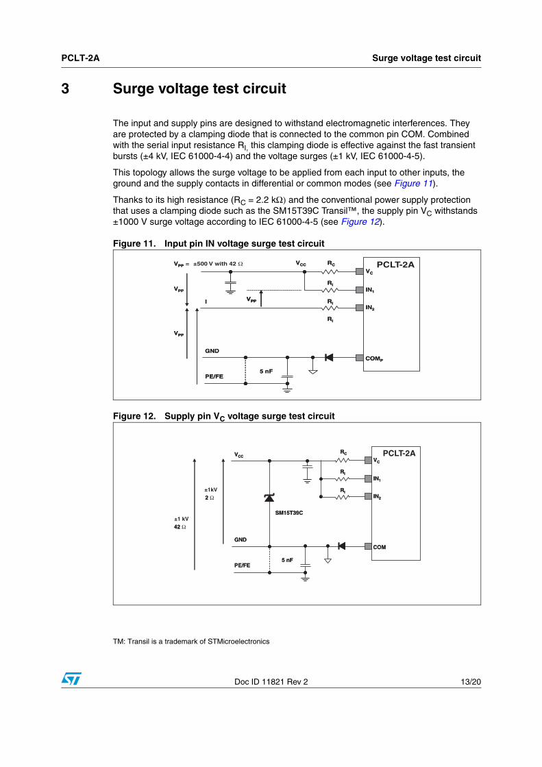
3 Surge voltage test circuit
The input and supply pins are designed to withstand electromagnetic interferences. They are protected by a clamping diode that is connected to the common pin COM. Combined with the serial input resistance RI, this clamping diode is effective against the fast transient bursts (±4 kV, IEC 61000-4-4) and the voltage surges (±1 kV, IEC 61000-4-5).
This topology allows the surge voltage to be applied from each input to other inputs, the ground and the supply contacts in differential or common modes (see Figure 11).
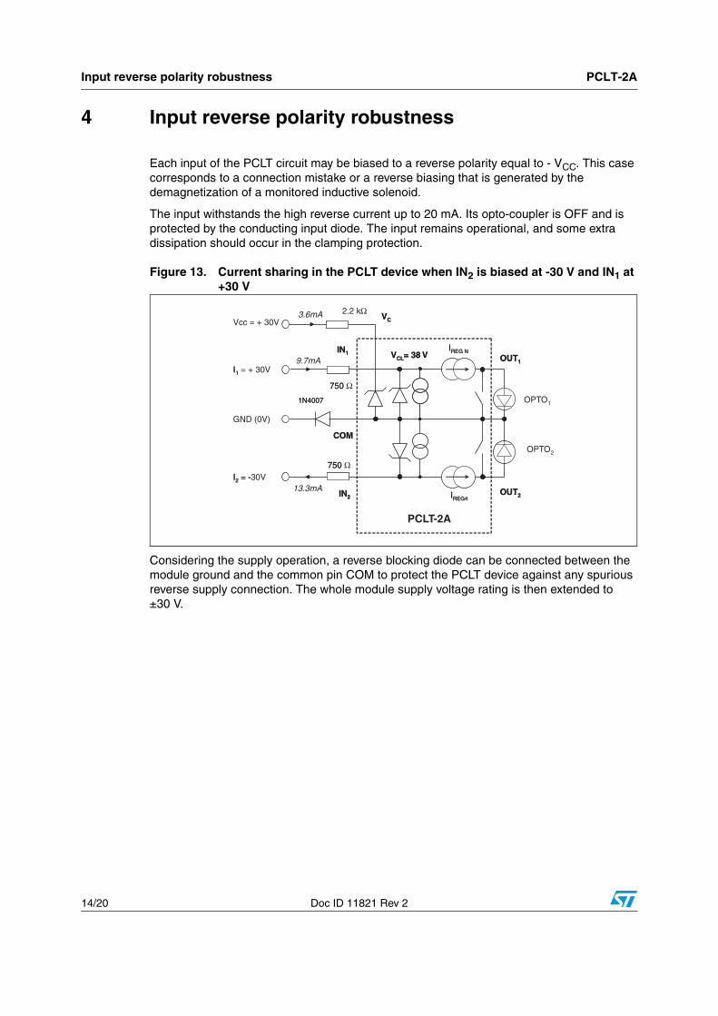
Thanks to its high resistance (RC = 2.2 kΩ) and the conventional power supply protection that uses a clamping diode such as the SM15T39C Transil™, the supply pin VC withstands ±1000 V surge voltage according to IEC 61000-4-5 (see Figure 12).
Figure 11. Input pin IN voltage surge test circuit
Figure 12. Supply pin VC voltage surge test circuit
TM: Transil is a trademark of STMicroelectronics
RIIN1
RIIN2
RI
RC
VC
COMP
VCC
GND
PE/FE
I
VPP
VPP
5 nF
VPP
VPP
RIIN1
RIIN2
RI
RC
VC
COMP
VCC
GND
PE/FE
PCLT-2A
I
VPP
VPP
5 nF
VPP = ±500 V with 42 Ω
VPPVPP
±1 kV42 Ω
RIIN1
RIIN2
RC
VC
COM
VCC
GND
PE/FE5 nF
SM15T39C
±1kV2 Ω
42
RIIN1
RIIN2
RC
VC
COM
VCC
GND
PE/FE
PCLT-2A
5 nF
SM15T39C
2
Input reverse polarity robustness PCLT-2A
14/20 Doc ID 11821 Rev 2
4 Input reverse polarity robustness
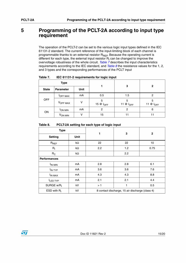
Each input of the PCLT circuit may be biased to a reverse polarity equal to - VCC. This case corresponds to a connection mistake or a reverse biasing that is generated by the demagnetization of a monitored inductive solenoid.
The input withstands the high reverse current up to 20 mA. Its opto-coupler is OFF and is protected by the conducting input diode. The input remains operational, and some extra dissipation should occur in the clamping protection.
Figure 13. Current sharing in the PCLT device when IN2 is biased at -30 V and IN1 at +30 V
Considering the supply operation, a reverse blocking diode can be connected between the module ground and the common pin COM to protect the PCLT device against any spurious reverse supply connection. The whole module supply voltage rating is then extended to ±30 V.
OPTO1
OPTO2
Ω
750
750 Ω
I1 = + 30V
I2 = -30V
GND (0V)
Vcc = + 30V
COM
OUT1
OUT2IREG4
1N4007
VC
PCLT-2A
IN2
IN1IREG NVCL= 38 V
2.2 k
750 Ω
750
I1
I2 = -
3.6mA
9.7mA
13.3mA
COM
OUT1
OUT2IREG4
1N4007
VC
IN2
IN1IREG NVCL= 38 V
PCLT-2A Programming of the PCLT-2A according to input type requirement
Doc ID 11821 Rev 2 15/20
5 Programming of the PCLT-2A according to input type requirement
The operation of the PCLT-2 can be set to the various logic input types defined in the IEC 61131-2 standard. The current reference of the input-limiting block of each channel is programmable thanks to an external resistor RREF. Because the operating current is different for each type, the external input resistor RI can be changed to improve the overvoltage robustness of the whole circuit. Table 7 describes the input characteristics requirements according to the IEC standard, and Table 8 the resistance values for the 1, 2, and 3 types and the corresponding performances of the PCLT input
.
.
Table 7. IEC 61131-2 requirements for logic input
Type1 3 2
State Parameter Unit
OFF
IOFF MAX mA 0.5 1.5 2
VOFF MAX V5
15 @ IOFF
511 @ IOFF
511 @ IOFF
ONION MIN mA 2 2 6
VON MIN V 15 11 11
Table 8. PCLT-2A setting for each type of logic input
Type1 3 2
Setting Unit
RREF kΩ 22 22 10
RI kΩ 2.2 1.2 0.75
RC kΩ 2.2
Performances
IIN MIN mA 2.8 2.8 6.1
IIN TYP mA 3.6 3.6 7.6
IIN MAX mA 4.3 4.3 8.8
ILED TYP mA 2.1 2.1 4.4
SURGE w/RI kV > 1 1 0.5
ESD with RI kV 8 contact discharge, 15 air discharge (class 4)
Unisolated AS-Interface bus application diagram PCLT-2A
16/20 Doc ID 11821 Rev 2
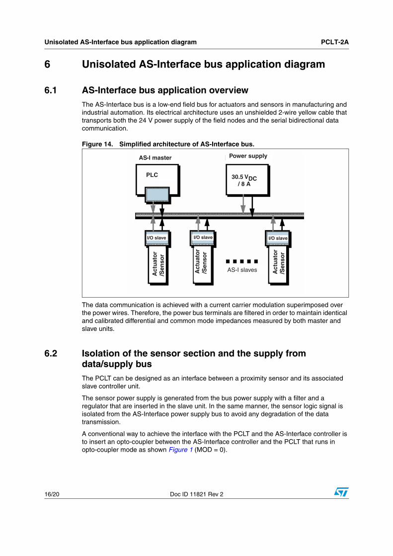
6 Unisolated AS-Interface bus application diagram
6.1 AS-Interface bus application overviewThe AS-Interface bus is a low-end field bus for actuators and sensors in manufacturing and industrial automation. Its electrical architecture uses an unshielded 2-wire yellow cable that transports both the 24 V power supply of the field nodes and the serial bidirectional data communication.
Figure 14. Simplified architecture of AS-Interface bus.
The data communication is achieved with a current carrier modulation superimposed over the power wires. Therefore, the power bus terminals are filtered in order to maintain identical and calibrated differential and common mode impedances measured by both master and slave units.
6.2 Isolation of the sensor section and the supply from data/supply busThe PCLT can be designed as an interface between a proximity sensor and its associated slave controller unit.
The sensor power supply is generated from the bus power supply with a filter and a regulator that are inserted in the slave unit. In the same manner, the sensor logic signal is isolated from the AS-Interface power supply bus to avoid any degradation of the data transmission.
A conventional way to achieve the interface with the PCLT and the AS-Interface controller is to insert an opto-coupler between the AS-Interface controller and the PCLT that runs in opto-coupler mode as shown Figure 1 (MOD = 0).
I/O SLAVE
AS-i SLAVES
AS-i MASTER
I/O SLAVE I/O SLAVEI/O SLAVE
AS-I slaves
AS-I master
I/O SLAVE I/O SLAVE
Power supply
I/O slave I/O slave I/O slave
Act
uat
or
/Sen
sor
Act
uat
or
/Sen
sor
Act
uat
or
/Sen
sor
PLC 30.5 VDC/ 8 A
PCLT-2A Unisolated AS-Interface bus application diagram
Doc ID 11821 Rev 2 17/20
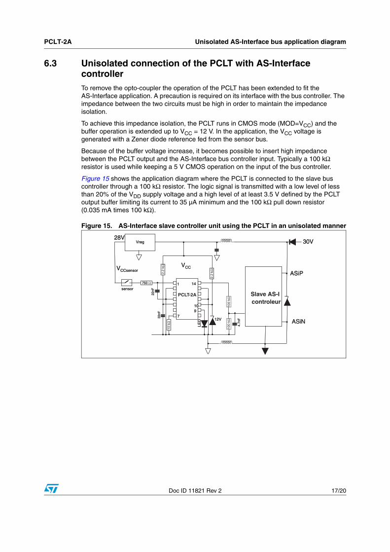
6.3 Unisolated connection of the PCLT with AS-Interface controllerTo remove the opto-coupler the operation of the PCLT has been extended to fit the AS-Interface application. A precaution is required on its interface with the bus controller. The impedance between the two circuits must be high in order to maintain the impedance isolation.
To achieve this impedance isolation, the PCLT runs in CMOS mode (MOD=VCC) and the buffer operation is extended up to VCC = 12 V. In the application, the VCC voltage is generated with a Zener diode reference fed from the sensor bus.
Because of the buffer voltage increase, it becomes possible to insert high impedance between the PCLT output and the AS-Interface bus controller input. Typically a 100 kΩ resistor is used while keeping a 5 V CMOS operation on the input of the bus controller.
Figure 15 shows the application diagram where the PCLT is connected to the slave bus controller through a 100 kΩ resistor. The logic signal is transmitted with a low level of less than 20% of the VDD supply voltage and a high level of at least 3.5 V defined by the PCLT output buffer limiting its current to 35 µA minimum and the 100 kΩ pull down resistor(0.035 mA times 100 kΩ).
Figure 15. AS-Interface slave controller unit using the PCLT in an unisolated manner
10
12V
VCC
28V
1
4.7n
F
750
7
14
9
LED
22nF
VCCsensor
33nF
sensor
Vreg
ASiP
ASiN
30V
10
12V
Slave AS-Icontroleur
VCC
28V
1
PCLT-2A
4.7n
F
750 Ω
7
14
9
LED
22nF
VCCsensor
33nF
sensor
Vreg
ASiP
ASiN
30V
100
kΩ10
0 kΩ
10 k
Ω
2.2
kΩ2.2
kΩ
Package information PCLT-2A
18/20 Doc ID 11821 Rev 2
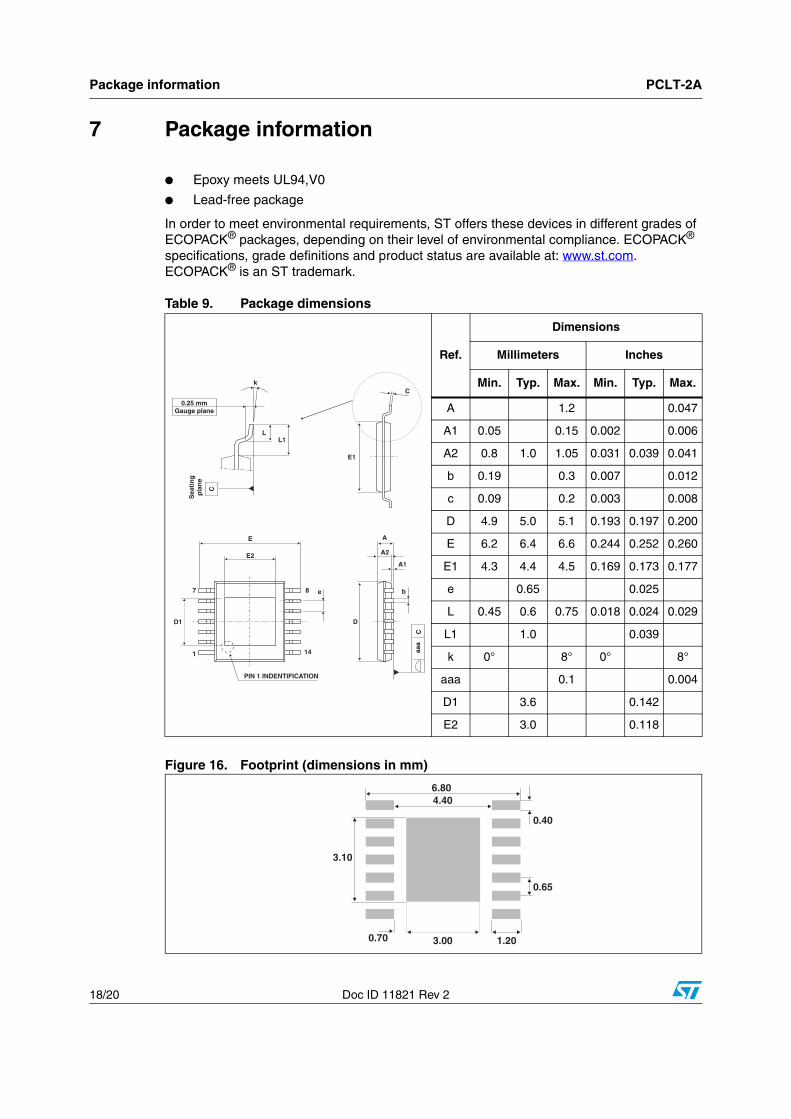
7 Package information
● Epoxy meets UL94,V0
● Lead-free package
In order to meet environmental requirements, ST offers these devices in different grades of ECOPACK® packages, depending on their level of environmental compliance. ECOPACK® specifications, grade definitions and product status are available at: www.st.com. ECOPACK® is an ST trademark.
Figure 16. Footprint (dimensions in mm)
Table 9. Package dimensions
Ref.
Dimensions
Millimeters Inches
Min. Typ. Max. Min. Typ. Max.
A 1.2 0.047
A1 0.05 0.15 0.002 0.006
A2 0.8 1.0 1.05 0.031 0.039 0.041
b 0.19 0.3 0.007 0.012
c 0.09 0.2 0.003 0.008
D 4.9 5.0 5.1 0.193 0.197 0.200
E 6.2 6.4 6.6 0.244 0.252 0.260
E1 4.3 4.4 4.5 0.169 0.173 0.177
e 0.65 0.025
L 0.45 0.6 0.75 0.018 0.024 0.029
L1 1.0 0.039
k 0° 8° 0° 8°
aaa 0.1 0.004
D1 3.6 0.142
E2 3.0 0.118
C
E1
E
E2
D1
A
A2
A1
b
D
aaa
C
C
Sea
tin
gp
lan
e
0.25 mmGauge plane
k
LL1
87
1 14
PIN 1 INDENTIFICATION
e
4.40
0.65
1.203.00
3.10
0.40
0.70
6.80

PCLT-2A Ordering information scheme
Doc ID 11821 Rev 2 19/20
8 Ordering information scheme
Figure 17. Ordering information scheme
9 Ordering information
10 Revision history
PCLT - 2 A T4
Programmable current limiting termination
Number of integrated channels2 = 2 channels
EMC levelA = 500 V according to IEC 61000-4-5 for type 2and 1000 V for type 3
Package
T4 = TSSOP14
Table 10. Ordering information
Ordering code Marking Package Weight Base qty Delivery mode
PCLT-2AT4PCLT-2AT4 TSSOP14(1)
1. Exposed pad version
0.057 g96 Tube
PCLT-2AT4-TR 2500 Tape and reel
Table 11. Document revision history
Date Revision Changes
16-Nov-2005 1 Initial release.
29-Mar-2012 2 Added ECOPACK statement.

PCLT-2A
20/20 Doc ID 11821 Rev 2
Please Read Carefully:
Information in this document is provided solely in connection with ST products. STMicroelectronics NV and its subsidiaries (“ST”) reserve theright to make changes, corrections, modifications or improvements, to this document, and the products and services described herein at anytime, without notice.
All ST products are sold pursuant to ST’s terms and conditions of sale.
Purchasers are solely responsible for the choice, selection and use of the ST products and services described herein, and ST assumes noliability whatsoever relating to the choice, selection or use of the ST products and services described herein.
No license, express or implied, by estoppel or otherwise, to any intellectual property rights is granted under this document. If any part of thisdocument refers to any third party products or services it shall not be deemed a license grant by ST for the use of such third party productsor services, or any intellectual property contained therein or considered as a warranty covering the use in any manner whatsoever of suchthird party products or services or any intellectual property contained therein.
UNLESS OTHERWISE SET FORTH IN ST’S TERMS AND CONDITIONS OF SALE ST DISCLAIMS ANY EXPRESS OR IMPLIEDWARRANTY WITH RESPECT TO THE USE AND/OR SALE OF ST PRODUCTS INCLUDING WITHOUT LIMITATION IMPLIEDWARRANTIES OF MERCHANTABILITY, FITNESS FOR A PARTICULAR PURPOSE (AND THEIR EQUIVALENTS UNDER THE LAWSOF ANY JURISDICTION), OR INFRINGEMENT OF ANY PATENT, COPYRIGHT OR OTHER INTELLECTUAL PROPERTY RIGHT.
UNLESS EXPRESSLY APPROVED IN WRITING BY TWO AUTHORIZED ST REPRESENTATIVES, ST PRODUCTS ARE NOTRECOMMENDED, AUTHORIZED OR WARRANTED FOR USE IN MILITARY, AIR CRAFT, SPACE, LIFE SAVING, OR LIFE SUSTAININGAPPLICATIONS, NOR IN PRODUCTS OR SYSTEMS WHERE FAILURE OR MALFUNCTION MAY RESULT IN PERSONAL INJURY,DEATH, OR SEVERE PROPERTY OR ENVIRONMENTAL DAMAGE. ST PRODUCTS WHICH ARE NOT SPECIFIED AS "AUTOMOTIVEGRADE" MAY ONLY BE USED IN AUTOMOTIVE APPLICATIONS AT USER’S OWN RISK.
Resale of ST products with provisions different from the statements and/or technical features set forth in this document shall immediately voidany warranty granted by ST for the ST product or service described herein and shall not create or extend in any manner whatsoever, anyliability of ST.
ST and the ST logo are trademarks or registered trademarks of ST in various countries.
Information in this document supersedes and replaces all information previously supplied.
The ST logo is a registered trademark of STMicroelectronics. All other names are the property of their respective owners.
© 2012 STMicroelectronics - All rights reserved
STMicroelectronics group of companies
Australia - Belgium - Brazil - Canada - China - Czech Republic - Finland - France - Germany - Hong Kong - India - Israel - Italy - Japan - Malaysia - Malta - Morocco - Philippines - Singapore - Spain - Sweden - Switzerland - United Kingdom - United States of America
www.st.com