LM2717 Dual Step-DownDC/DC Converter - Texas … Dual Step-DownDC/DC Converter Check for Samples:...
17
LM2717 www.ti.com SNVS253D – MAY 2005 – REVISED MARCH 2013 LM2717 Dual Step-Down DC/DC Converter Check for Samples: LM2717 1FEATURES DESCRIPTION The LM2717 is composed of two PWM DC/DC buck 2• Fixed 3.3V Output Buck Converter with a 2.2A, (step-down) converters. The first converter is used to 0.16Ω, Internal Switch generate a fixed output voltage of 3.3V. The second • Adjustable Buck Converter with a 3.2A, 0.16Ω, converter is used to generate an adjustable output Internal Switch voltage. Both converters feature low R DSON (0.16Ω) internal switches for maximum efficiency. Operating • Operating Input Voltage Range of 4V to 20V frequency can be adjusted anywhere between • Input Undervoltage Protection 300kHz and 600kHz allowing the use of small • 300kHz to 600kHz Pin Adjustable Operating external components. External soft-start pins for each Frequency enables the user to tailor the soft-start times to a specific application. Each converter may also be shut • Over Temperature Protection down independently with its own shutdown pin. The • Small 24-Lead TSSOP Package LM2717 is available in a low profile 24-lead TSSOP package ensuring a low profile overall solution. APPLICATIONS • TFT-LCD Displays • Handheld Devices • Portable Applications • Laptop Computers Typical Application Circuit 1 Please be aware that an important notice concerning availability, standard warranty, and use in critical applications of Texas Instruments semiconductor products and disclaimers thereto appears at the end of this data sheet. 2All trademarks are the property of their respective owners. PRODUCTION DATA information is current as of publication date. Copyright © 2005–2013, Texas Instruments Incorporated Products conform to specifications per the terms of the Texas Instruments standard warranty. Production processing does not necessarily include testing of all parameters.
Transcript of LM2717 Dual Step-DownDC/DC Converter - Texas … Dual Step-DownDC/DC Converter Check for Samples:...
LM2717
www.ti.com SNVS253D –MAY 2005–REVISED MARCH 2013
LM2717 Dual Step-Down DC/DC ConverterCheck for Samples: LM2717
1FEATURES DESCRIPTIONThe LM2717 is composed of two PWM DC/DC buck
2• Fixed 3.3V Output Buck Converter with a 2.2A,(step-down) converters. The first converter is used to0.16Ω, Internal Switchgenerate a fixed output voltage of 3.3V. The second
• Adjustable Buck Converter with a 3.2A, 0.16Ω, converter is used to generate an adjustable outputInternal Switch voltage. Both converters feature low RDSON (0.16Ω)
internal switches for maximum efficiency. Operating• Operating Input Voltage Range of 4V to 20Vfrequency can be adjusted anywhere between• Input Undervoltage Protection300kHz and 600kHz allowing the use of small
• 300kHz to 600kHz Pin Adjustable Operating external components. External soft-start pins for eachFrequency enables the user to tailor the soft-start times to a
specific application. Each converter may also be shut• Over Temperature Protectiondown independently with its own shutdown pin. The• Small 24-Lead TSSOP PackageLM2717 is available in a low profile 24-lead TSSOPpackage ensuring a low profile overall solution.APPLICATIONS
• TFT-LCD Displays• Handheld Devices• Portable Applications• Laptop Computers
Typical Application Circuit
1
Please be aware that an important notice concerning availability, standard warranty, and use in critical applications ofTexas Instruments semiconductor products and disclaimers thereto appears at the end of this data sheet.
2All trademarks are the property of their respective owners.
PRODUCTION DATA information is current as of publication date. Copyright © 2005–2013, Texas Instruments IncorporatedProducts conform to specifications per the terms of the TexasInstruments standard warranty. Production processing does notnecessarily include testing of all parameters.
LM2717
SNVS253D –MAY 2005–REVISED MARCH 2013 www.ti.com
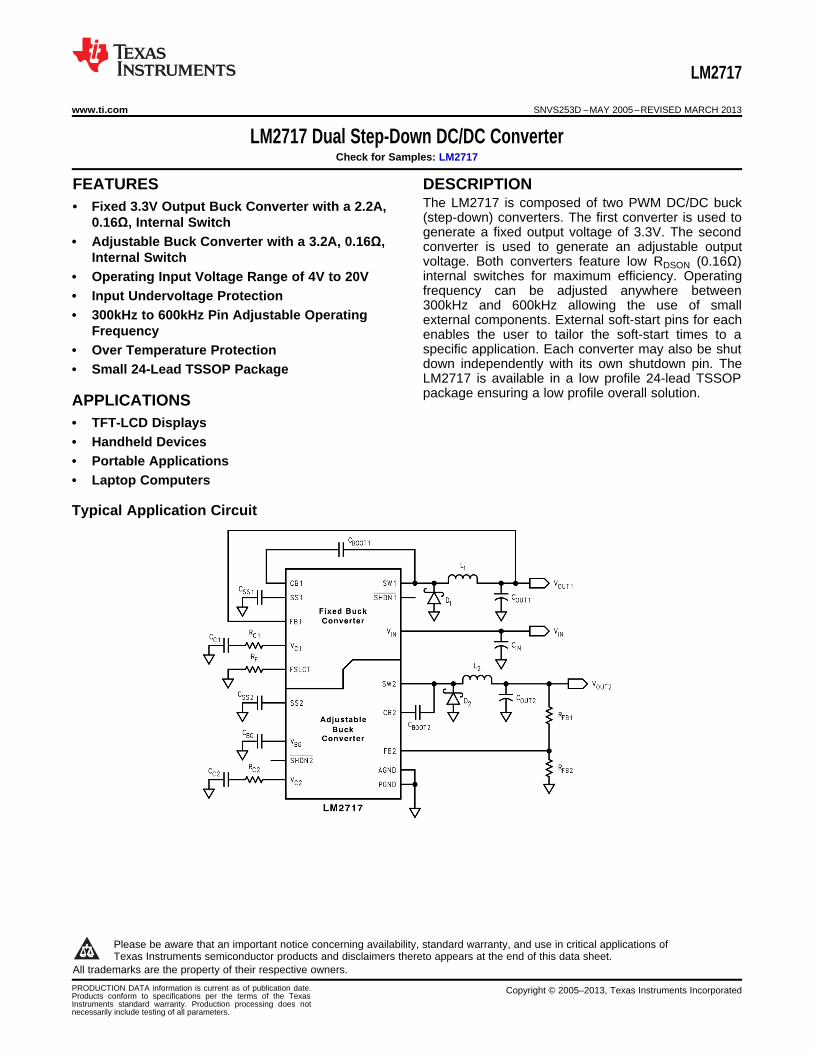
Connection Diagram
Top View
Figure 1. 24-Lead TSSOPSee Package Number PW0024A
PIN DESCRIPTIONSPin Name Function
1 PGND Power ground. PGND and AGND pins must be connected together directly at the part.
2 PGND Power ground. PGND and AGND pins must be connected together directly at the part.
3 AGND Analog ground. PGND and AGND pins must be connected together directly at the part.
4 FB1 Fixed buck output voltage feedback input.
5 VC1 Fixed buck compensation network connection. Connected to the output of the voltage error amplifier.
6 VBG Bandgap connection.
7 VC2 Adjustable buck compensation network connection. Connected to the output of the voltage erroramplifier.
8 FB2 Adjustable buck output voltage feedback input.
9 AGND Analog ground. PGND and AGND pins must be connected together directly at the part.
10 AGND Analog ground. PGND and AGND pins must be connected together directly at the part.
11 PGND Power ground. PGND and AGND pins must be connected together directly at the part.
12 PGND Power ground. PGND and AGND pins must be connected together directly at the part.
13 SW2 Adjustable buck power switch input. Switch connected between VIN pins and SW2 pin.
14 VIN Analog power input. VIN pins should be connected together directly at the part.
15 VIN Analog power input. VIN pins should be connected together directly at the part.
16 CB2 Adjustable buck converter bootstrap capacitor connection.
17 SHDN2 Shutdown pin for adjustable buck converter. Active low.
18 SS2 Adjustable buck soft start pin.
19 FSLCT Switching frequency select input. Use a resistor to set the frequency anywhere between 300kHz and600kHz.
20 SS1 Fixed buck soft start pin.
21 SHDN1 Shutdown pin for fixed buck converter. Active low.
22 CB1 Fixed buck converter bootstrap capacitor connection.
23 VIN Analog power input. VIN pins should be connected together directly at the part.
24 SW1 Fixed buck power switch input. Switch connected between VIN pins and SW1 pin.
2 Submit Documentation Feedback Copyright © 2005–2013, Texas Instruments Incorporated
Product Folder Links: LM2717
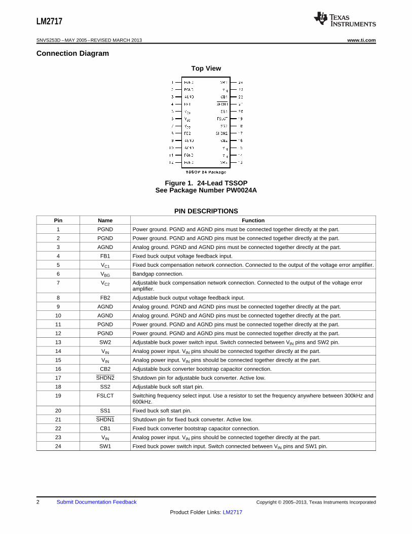
95% DutyCycle Limit
OSC
FSLCT
DCLIMIT
SET
++
-
+PWMComp RESET
-
+OVPComp
BuckDriver
BUCKDRIVE
+
-ErrorAmp
BG
FB1
Bandgap
SoftStart
ThermalShutdown
VBG VC1
OVP
TSH
SHDN1
SD
Buck LoadCurrent
Measurement
Fixed Buck Converter
CB1
SS1
SW1
VIN
PGND
95% DutyCycle Limit
OSC
FSLCT
DCLIMIT
SET
++
-
+PWMComp RESET
-
+OVPComp
BuckDriver
BUCKDRIVE
+
-ErrorAmp
BG
FB2
Bandgap
SoftStart
ThermalShutdown
VBG VC2
OVP
TSH
SHDN2
SD
Buck LoadCurrent
Measurement
Adjustable Buck Converter
CB2
SS2
SW2
VIN
PGND
36.5k
20.38k
LM2717
www.ti.com SNVS253D –MAY 2005–REVISED MARCH 2013
Block Diagram
These devices have limited built-in ESD protection. The leads should be shorted together or the device placed in conductive foamduring storage or handling to prevent electrostatic damage to the MOS gates.
Copyright © 2005–2013, Texas Instruments Incorporated Submit Documentation Feedback 3
Product Folder Links: LM2717
LM2717
SNVS253D –MAY 2005–REVISED MARCH 2013 www.ti.com
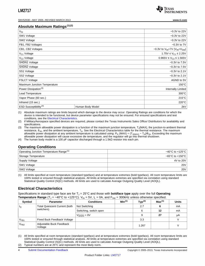
Absolute Maximum Ratings (1) (2)
VIN −0.3V to 22V
SW1 Voltage −0.3V to 22V
SW2 Voltage −0.3V to 22V
FB1, FB2 Voltages −0.3V to 7V
CB1, CB2 Voltages −0.3V to VIN+7V (VIN=VSW)
VC1 Voltage 1.75V ≤ VC1 ≤ 2.25V
VC2 Voltage 0.965V ≤ VC2 ≤ 1.565V
SHDN1 Voltage −0.3V to 7.5V
SHDN2 Voltage −0.3V to 7.5V
SS1 Voltage −0.3V to 2.1V
SS2 Voltage −0.3V to 2.1V
FSLCT Voltage AGND to 5V
Maximum Junction Temperature 150°C
Power Dissipation (3) Internally Limited
Lead Temperature 300°C
Vapor Phase (60 sec.) 215°C
Infrared (15 sec.) 220°C
ESD Susceptibility (4) Human Body Model 2kV
(1) Absolute maximum ratings are limits beyond which damage to the device may occur. Operating Ratings are conditions for which thedevice is intended to be functional, but device parameter specifications may not be ensured. For ensured specifications and testconditions, see the Electrical Characteristics.
(2) If Military/Aerospace specified devices are required, please contact the Texas Instruments Sales Office/ Distributors for availability andspecifications.
(3) The maximum allowable power dissipation is a function of the maximum junction temperature, TJ(MAX), the junction-to-ambient thermalresistance, θJA, and the ambient temperature, TA. See the Electrical Characteristics table for the thermal resistance. The maximumallowable power dissipation at any ambient temperature is calculated using: PD (MAX) = (TJ(MAX) − TA)/θJA. Exceeding the maximumallowable power dissipation will cause excessive die temperature, and the regulator will go into thermal shutdown.
(4) The human body model is a 100 pF capacitor discharged through a 1.5kΩ resistor into each pin.
Operating ConditionsOperating Junction Temperature Range (1) −40°C to +125°C
Storage Temperature −65°C to +150°C
Supply Voltage 4V to 20V
SW1 Voltage 20V
SW2 Voltage 20V
(1) All limits specified at room temperature (standard typeface) and at temperature extremes (bold typeface). All room temperature limits are100% tested or ensured through statistical analysis. All limits at temperature extremes are specified via correlation using standardStatistical Quality Control (SQC) methods. All limits are used to calculate Average Outgoing Quality Level (AOQL).
Electrical CharacteristicsSpecifications in standard type face are for TJ = 25°C and those with boldface type apply over the full OperatingTemperature Range (TJ = −40°C to +125°C). VIN = 5V, IL = 0A, and FSW = 300kHz unless otherwise specified.
Symbol Parameter Conditions Min (1) Typ (2) Max (1) Units
IQ Total Quiescent Current (both Not Switching 2.7 6 mAswitchers) Switching, switch open 6 12 mA
VSHDN = 0V 9 27 µA
VFB1 Fixed Buck Feedback Voltage 3.3 V
VFB2 Adjustable Buck Feedback 1.267 VVoltage
(1) All limits specified at room temperature (standard typeface) and at temperature extremes (bold typeface). All room temperature limits are100% tested or ensured through statistical analysis. All limits at temperature extremes are specified via correlation using standardStatistical Quality Control (SQC) methods. All limits are used to calculate Average Outgoing Quality Level (AOQL).
(2) Typical numbers are at 25°C and represent the most likely norm.
4 Submit Documentation Feedback Copyright © 2005–2013, Texas Instruments Incorporated
Product Folder Links: LM2717
LM2717
www.ti.com SNVS253D –MAY 2005–REVISED MARCH 2013
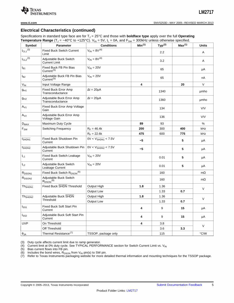
Electrical Characteristics (continued)Specifications in standard type face are for TJ = 25°C and those with boldface type apply over the full OperatingTemperature Range (TJ = −40°C to +125°C). VIN = 5V, IL = 0A, and FSW = 300kHz unless otherwise specified.
Symbol Parameter Conditions Min (1) Typ (2) Max (1) Units
ICL1(3) Fixed Buck Switch Current VIN = 8V (4)
2.2 ALimit
ICL2(3) Adjustable Buck Switch VIN = 8V (4)
3.2 ACurrent Limit
IB1 Fixed Buck FB Pin Bias VIN = 20V 65 µACurrent (5)
IB2 Adjustable Buck FB Pin Bias VIN = 20V 65 nACurrent (5)
VIN Input Voltage Range 4 20 V
gm1 Fixed Buck Error Amp ΔI = 20µA 1340 µmhoTransconductance
gm2 Adjustable Buck Error Amp ΔI = 20µA 1360 µmhoTransconductance
AV1 Fixed Buck Error Amp Voltage 134 V/VGain
AV2 Adjustable Buck Error Amp 136 V/VVoltage Gain
DMAX Maximum Duty Cycle 89 93 %
FSW Switching Frequency RF = 46.4k 200 300 400 kHz
RF = 22.6k 475 600 775 kHz
ISHDN1 Fixed Buck Shutdown Pin 0V < VSHDN1 < 7.5V −5 5 µACurrent
ISHDN2 Adjustable Buck Shutdown Pin 0V < VSHDN2 < 7.5V −5 5 µACurrent
IL1 Fixed Buck Switch Leakage VIN = 20V 0.01 5 µACurrent
IL2 Adjustable Buck Switch VIN = 20V 0.01 5 µALeakage Current
RDSON1 Fixed Buck Switch RDSON(6) 160 mΩ
RDSON2 Adjustable Buck Switch 160 mΩRDSON(6)
ThSHDN1 Fixed Buck SHDN Threshold Output High 1.8 1.36V
Output Low 1.33 0.7
ThSHDN2 Adjustable Buck SHDN Output High 1.8 1.36VThreshold Output Low 1.33 0.7
ISS1 Fixed Buck Soft Start Pin 4 9 15 µACurrent
ISS2 Adjustable Buck Soft Start Pin 4 9 15 µACurrent
UVP On Threshold 4 3.8V
Off Threshold 3.6 3.3
θJA Thermal Resistance (7) TSSOP, package only 115 °C/W
(3) Duty cycle affects current limit due to ramp generator.(4) Current limit at 0% duty cycle. See TYPICAL PERFORMANCE section for Switch Current Limit vs. VIN(5) Bias current flows into FB pin.(6) Includes the bond wires, RDSON from VIN pin(s) to SW pin.(7) Refer to Texas Instruments packaging website for more detailed thermal information and mounting techniques for the TSSOP package.
Copyright © 2005–2013, Texas Instruments Incorporated Submit Documentation Feedback 5
Product Folder Links: LM2717
4 6 8 10 12 14 16 18 20
INPUT VOLTAGE (V)
100
110
120
130
140
150
160
170
180
190
200
SW
ITC
H R
DS
(ON
) (m:
0 0.2 0.4 0.6 0.8 1 1.2 1.4 1.6
LOAD CURRENT (A)
0
10
20
30
40
50
60
70
80
90
100V IN = 5V
V IN = 12V
V IN = 18V
EF
FIC
IEN
CY
(%
)
4 6 8 10 12 14 16 18 20
INPUT VOLTAGE (V)
100
110
120
130
140
150
160
170
180
190
200
SW
ITC
H R
DS
(ON
) (m:
4 6 8 10 12 14 16 18 20
INPUT VOLTAGE (V)
290
295
300
305
310
315
320
R F = 46.4k
SW
ITC
HIN
G F
RE
QU
EN
CY
(k
Hz)
4 6 8 10 12 14 16 18 20
INPUT VOLTAGE (V)
0
1
2
3
4
5
6
7
8
9
QU
IES
CE
NT
CU
RR
EN
T (
mA
)
4 6 8 10 12 14 16 18 20
INPUT VOLTAGE (V)
QU
IES
CE
NT
CU
RR
EN
T (P
A)
0
2
4
6
8
10
12
14
16
LM2717
SNVS253D –MAY 2005–REVISED MARCH 2013 www.ti.com
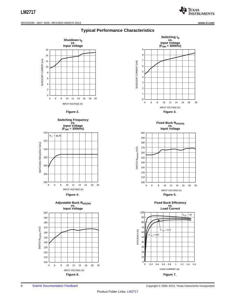
Typical Performance Characteristics
Switching IQShutdown IQ vs.
vs. Input VoltageInput Voltage (FSW = 300kHz)
Figure 2. Figure 3.
Switching Frequencyvs. Fixed Buck RDS(ON)
Input Voltage vs.(FSW = 300kHz) Input Voltage
Figure 4. Figure 5.
Adjustable Buck RDS(ON) Fixed Buck Efficiencyvs. vs.
Input Voltage Load Current
Figure 6. Figure 7.
6 Submit Documentation Feedback Copyright © 2005–2013, Texas Instruments Incorporated
Product Folder Links: LM2717
4 6 8 10 12 14 16 18 20
INPUT VOLTAGE (V)
1
1.2
1.4
1.6
1.8
2
2.2
2.4
SW
ITC
H C
UR
RE
NT
LIM
IT (
A)
8 10 12 14 16 18 20
INPUT VOLTAGE (V)
SW
ITC
H C
UR
RE
NT
LIM
IT (
A)
2
2.2
2.4
2.6
2.8
3
3.2
3.4
0 0.5 1 1.5 2 2.5
LOAD CURRENT (A)
0
10
20
30
40
50
60
70
80
90
100
EF
FIC
IEN
CY
(%
)
V IN = 18V
0 0.5 1 1.5 2 2.5
LOAD CURRENT (A)
0
10
20
30
40
50
60
70
80
90
100
EF
FIC
IEN
CY
(%
)
V IN = 18V
LM2717
www.ti.com SNVS253D –MAY 2005–REVISED MARCH 2013
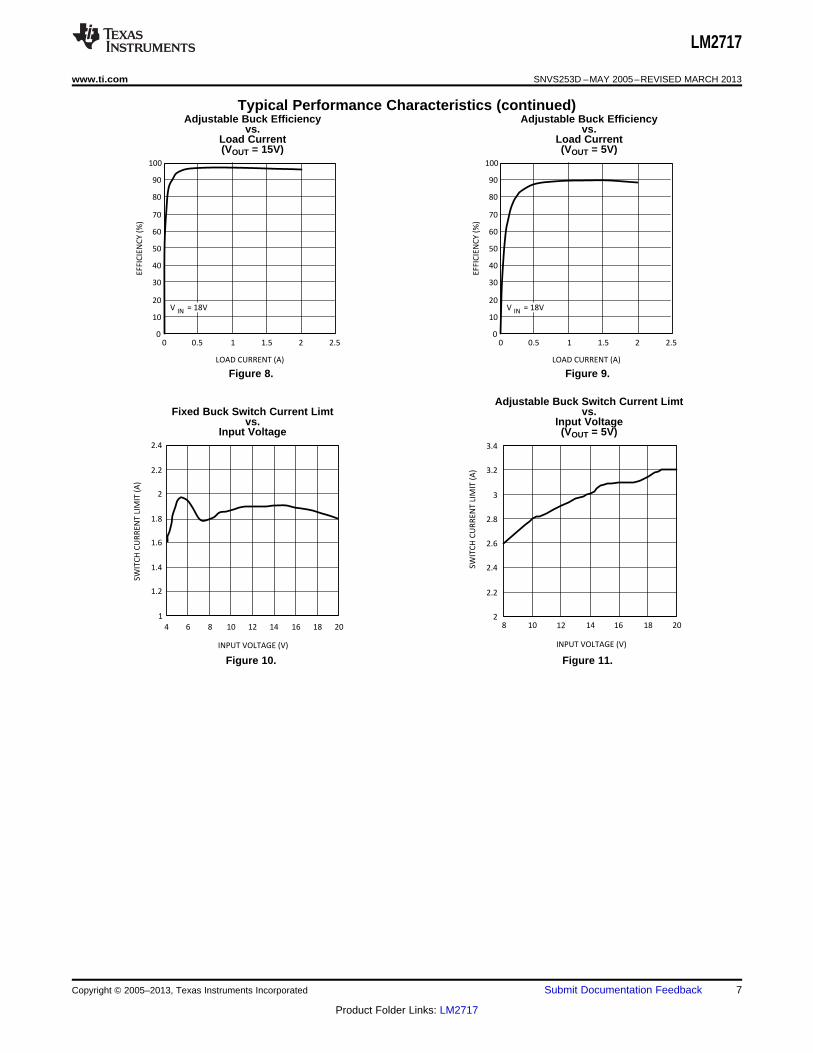
Typical Performance Characteristics (continued)Adjustable Buck Efficiency Adjustable Buck Efficiency
vs. vs.Load Current Load Current(VOUT = 15V) (VOUT = 5V)
Figure 8. Figure 9.
Adjustable Buck Switch Current LimtFixed Buck Switch Current Limt vs.
vs. Input VoltageInput Voltage (VOUT = 5V)
Figure 10. Figure 11.
Copyright © 2005–2013, Texas Instruments Incorporated Submit Documentation Feedback 7
Product Folder Links: LM2717
:RFB1 = RFB2 xVOUT - 1.267
1.267
VOUT VIN
, D' = (1-D) D =
LM2717
SNVS253D –MAY 2005–REVISED MARCH 2013 www.ti.com
BUCK OPERATION
PROTECTION (BOTH REGULATORS)
The LM2717 has dedicated protection circuitry running during normal operation to protect the IC. The ThermalShutdown circuitry turns off the power devices when the die temperature reaches excessive levels. The UVPcomparator protects the power devices during supply power startup and shutdown to prevent operation atvoltages less than the minimum input voltage. The OVP comparator is used to prevent the output voltage fromrising at no loads allowing full PWM operation over all load conditions. The LM2717 also features a shutdownmode for each converter decreasing the supply current to approximately 10µA (both in shutdown mode).
CONTINUOUS CONDUCTION MODE
The LM2717 contains current-mode, PWM buck regulators. A buck regulator steps the input voltage down to alower output voltage. In continuous conduction mode (when the inductor current never reaches zero at steadystate), the buck regulator operates in two cycles. The power switch is connected between VIN and SW1 andSW2.
In the first cycle of operation the transistor is closed and the diode is reverse biased. Energy is collected in theinductor and the load current is supplied by COUT and the rising current through the inductor.
During the second cycle the transistor is open and the diode is forward biased due to the fact that the inductorcurrent cannot instantaneously change direction. The energy stored in the inductor is transferred to the load andoutput capacitor.
The ratio of these two cycles determines the output voltage. The output voltage is defined approximately as:
(1)
where D is the duty cycle of the switch, D and D′ will be required for design calculations.
DESIGN PROCEDURE
This section presents guidelines for selecting external components.
SETTING THE OUTPUT VOLTAGE (ADJUSTABLE REGULATOR)
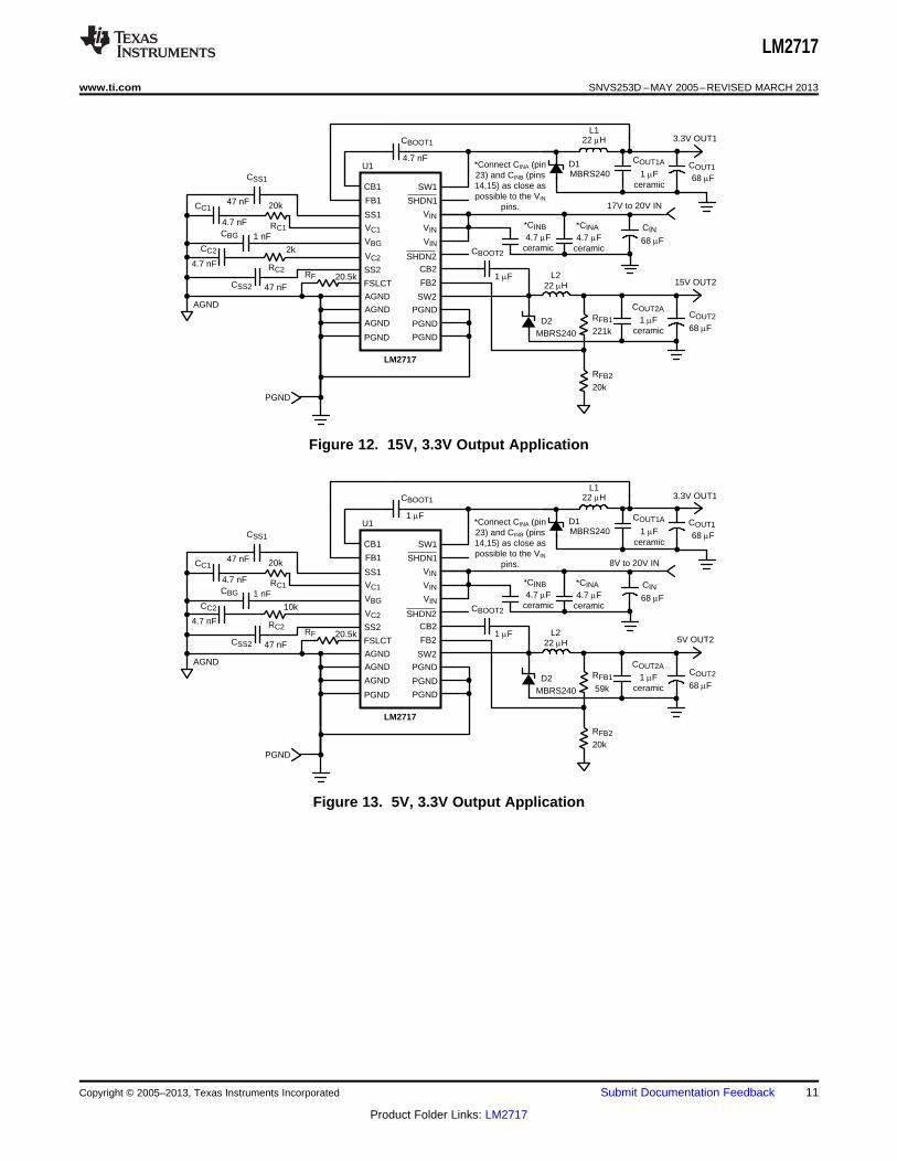
The output voltage is set using the feedback pin and a resistor divider connected to the output as shown inFigure 12. The feedback pin voltage is 1.26V, so the ratio of the feedback resistors sets the output voltageaccording to the following equation:
(2)
INPUT CAPACITOR
A low ESR aluminum, tantalum, or ceramic capacitor is needed betwen the input pin and power ground. Thiscapacitor prevents large voltage transients from appearing at the input. The capacitor is selected based on theRMS current and voltage requirements. The RMS current is given by:
(3)
The RMS current reaches its maximum (IOUT/2) when VIN equals 2VOUT. This value should be calculated for bothregulators and added to give a total RMS current rating. For an aluminum or ceramic capacitor, the voltage ratingshould be at least 25% higher than the maximum input voltage. If a tantalum capacitor is used, the voltage ratingrequired is about twice the maximum input voltage. The tantalum capacitor should be surge current tested by themanufacturer to prevent being shorted by the inrush current. The minimum capacitor value should be 47µF forlower output load current applications and less dynamic (quickly changing) load conditions. For higher outputcurrent applications or dynamic load conditions a 68µF to 100µF low ESR capacitor is recommended. It is alsorecommended to put a small ceramic capacitor (0.1µF to 4.7µF) between the input pins and ground to reducehigh frequency spikes.
8 Submit Documentation Feedback Copyright © 2005–2013, Texas Instruments Incorporated
Product Folder Links: LM2717
LM2717
www.ti.com SNVS253D –MAY 2005–REVISED MARCH 2013
INDUCTOR SELECTION
The most critical parameters for the inductor are the inductance, peak current and the DC resistance. Theinductance is related to the peak-to-peak inductor ripple current, the input and the output voltages (for 300kHzoperation):
(4)
A higher value of ripple current reduces inductance, but increases the conductance loss, core loss, and currentstress for the inductor and switch devices. It also requires a bigger output capacitor for the same output voltageripple requirement. A reasonable value is setting the ripple current to be 30% of the DC output current. Since theripple current increases with the input voltage, the maximum input voltage is always used to determine theinductance. The DC resistance of the inductor is a key parameter for the efficiency. Lower DC resistance isavailable with a bigger winding area. A good tradeoff between the efficiency and the core size is letting theinductor copper loss equal 2% of the output power.
OUTPUT CAPACITOR
The selection of COUT is driven by the maximum allowable output voltage ripple. The output ripple in the constantfrequency, PWM mode is approximated by:
(5)
The ESR term usually plays the dominant role in determining the voltage ripple. Low ESR ceramic, aluminumelectrolytic, or tantalum capacitors (such as Taiyo Yuden MLCC, Nichicon PL series, Sanyo OS-CON, Sprague593D, 594D, AVX TPS, and CDE polymer aluminum) is recommended. An electrolytic capacitor is notrecommended for temperatures below −25°C since its ESR rises dramatically at cold temperature. Ceramic ortantalum capacitors have much better ESR specifications at cold temperature and is preferred for lowtemperature applications.
BOOTSTRAP CAPACITOR
A 4.7nF ceramic capacitor or larger is recommended for the bootstrap capacitor. For applications where the inputvoltage is less than twice the output voltage a larger capacitor is recommended, generally 0.1µF to 1µF toensure plenty of gate drive for the internal switches and a consistently low RDS(ON).
SOFT-START CAPACITOR (BOTH REGULATORS)
The LM2717 does not contain internal soft-start which allows for fast startup time but also causes high inrushcurrent. Therefore for applications that need reduced inrush current the LM2717 has circuitry that is used to limitthe inrush current on start-up of the DC/DC switching regulators. This inrush current limiting circuitry serves as asoft-start. The external SS pins are used to tailor the soft-start for a specific application. A current (ISS) chargesthe external soft-start capacitor, CSS. The soft-start time can be estimated as:
TSS = CSS*0.6V/ISS (6)
When programming the softstart time simply use the equation given in the Soft-Start Capacitor section above.
SHUTDOWN OPERATION (BOTH REGULATORS)
The shutdown pins of the LM2717 are designed so that they may be controlled using 1.8V or higher logic signals.If the shutdown function is not to be used the pin may be left open. The maximum voltage to the shutdown pinshould not exceed 7.5V. If the use of a higher voltage is desired due to system or other constraints it may beused, however a 100k or larger resistor is recommended between the applied voltage and the shutdown pin toprotect the device.
SCHOTTKY DIODE
The breakdown voltage rating of D1 and D2 is preferred to be 25% higher than the maximum input voltage. Thecurrent rating for the diode should be equal to the maximum output current for best reliability in mostapplications. In cases where the input voltage is much greater than the output voltage the average diode currentis lower. In this case it is possible to use a diode with a lower average current rating, approximately (1-D)*IOUThowever the peak current rating should be higher than the maximum load current.
Copyright © 2005–2013, Texas Instruments Incorporated Submit Documentation Feedback 9
Product Folder Links: LM2717
LM2717
SNVS253D –MAY 2005–REVISED MARCH 2013 www.ti.com
LAYOUT CONSIDERATIONS
The LM2717 uses two separate ground connections, PGND for the drivers and boost NMOS power device andAGND for the sensitive analog control circuitry. The AGND and PGND pins should be tied directly together at thepackage. The feedback and compensation networks should be connected directly to a dedicated analog groundplane and this ground plane must connect to the AGND pin. If no analog ground plane is available then theground connections of the feedback and compensation networks must tie directly to the AGND pin. Connectingthese networks to the PGND can inject noise into the system and effect performance.
The input bypass capacitor CIN, as shown in Figure 12, must be placed close to the IC. This will reduce coppertrace resistance which effects input voltage ripple of the IC. For additional input voltage filtering, a 0.1µF to 4.7µFbypass capacitors can be placed in parallel with CIN, close to the VIN pins to shunt any high frequency noise toground. The output capacitors, COUT1 and COUT2, should also be placed close to the IC. Any copper traceconnections for the COUTX capacitors can increase the series resistance, which directly effects output voltageripple. The feedback network, resistors RFB1 and RFB2, should be kept close to the FB pin, and away from theinductor to minimize copper trace connections that can inject noise into the system. Trace connections made tothe inductors and schottky diodes should be minimized to reduce power dissipation and increase overallefficiency. For more detail on switching power supply layout considerations see Application Note AN-1149:Layout Guidelines for Switching Power Supplies (SNVA021).
Application Information
Table 1. Some Recommended Inductors (Others May Be Used)
Manufacturer Inductor Contact Information
Coilcraft DO3316 and DO5022 series www.coilcraft.com
Coiltronics DRQ73 and CD1 series www.cooperet.com
Pulse P0751 and P0762 series www.pulseeng.com
Sumida CDRH8D28 and CDRH8D43 series www.sumida.com
Table 2. Some Recommended Input And Output Capacitors (Others May Be Used)
Manufacturer Capacitor Contact Information
Vishay Sprague 293D, 592D, and 595D series tantalum www.vishay.com
Taiyo Yuden High capacitance MLCC ceramic www.t-yuden.com
ESRD seriec Polymer Aluminum ElectrolyticCornell Dubilier www.cde.comSPV and AFK series V-chip series
High capacitance MLCC ceramicPanasonic www.panasonic.comEEJ-L series tantalum
10 Submit Documentation Feedback Copyright © 2005–2013, Texas Instruments Incorporated
Product Folder Links: LM2717
PGND
FB1
VC1
VBG
SS2
VC2
FB2
AGND
AGND
PGND
PGND
PGND
SW1
VIN
CB1
SHDN1
SS1
FSLCT
SHDN2
SW2
LM2717
L222 PH
D2MBRS240
COUT2
68 PF
COUT1
3.3V OUT1
8V to 20V IN
5V OUT2
PGND
RFB1
59k
RFB2
20k
RF
*Connect CINA (pin 23) and CINB (pins 14,15) as close as possible to the VIN
pins.
68 PF
COUT1A
1 PF ceramic
L122 PH
D1MBRS240
1 PF
CBOOT1
*CINA CIN
68 PF
U1CSS1
CC1
CBG
CC2
CSS2
AGND
RC2
RC1
20k
10k
4.7 nF
1 nF
47 nF
4.7 nF
47 nF
VIN
VIN
CB2
AGND
*CINB4.7 PF
ceramic4.7 PF
ceramic
1 PF
CBOOT2
COUT2A
1 PF ceramic
20.5k
PGND
FB1
VC1
VBG
SS2
VC2
FB2
AGND
AGND
PGND
PGND
PGND
SW1
VIN
CB1
SHDN1
SS1
FSLCT
SHDN2
SW2
LM2717
L222 PH
D2MBRS240
COUT2
68 PF
COUT1
3.3V OUT1
17V to 20V IN
15V OUT2
PGND
RFB1
221k
RFB2
20k
RF
*Connect CINA (pin 23) and CINB (pins 14,15) as close as possible to the VIN
pins.
68 PF
COUT1A
1 PF ceramic
L122 PH
D1MBRS240
4.7 nF
CBOOT1
*CINA CIN
68 PF
U1CSS1
CC1
CBG
CC2
CSS2
AGND
RC2
RC1
20k
2k
4.7 nF
1 nF
47 nF
4.7 nF
47 nF
VIN
VIN
CB2
AGND
*CINB4.7 PF
ceramic4.7 PF
ceramic
1 PF
CBOOT2
COUT2A
1 PF ceramic
20.5k
LM2717
www.ti.com SNVS253D –MAY 2005–REVISED MARCH 2013
Figure 12. 15V, 3.3V Output Application
Figure 13. 5V, 3.3V Output Application
Copyright © 2005–2013, Texas Instruments Incorporated Submit Documentation Feedback 11
Product Folder Links: LM2717
LM2717
SNVS253D –MAY 2005–REVISED MARCH 2013 www.ti.com
REVISION HISTORY
Changes from Revision C (March 2013) to Revision D Page
• Changed layout of National Data Sheet to TI format .......................................................................................................... 11
12 Submit Documentation Feedback Copyright © 2005–2013, Texas Instruments Incorporated
Product Folder Links: LM2717
PACKAGE OPTION ADDENDUM
www.ti.com 7-Oct-2013
Addendum-Page 1
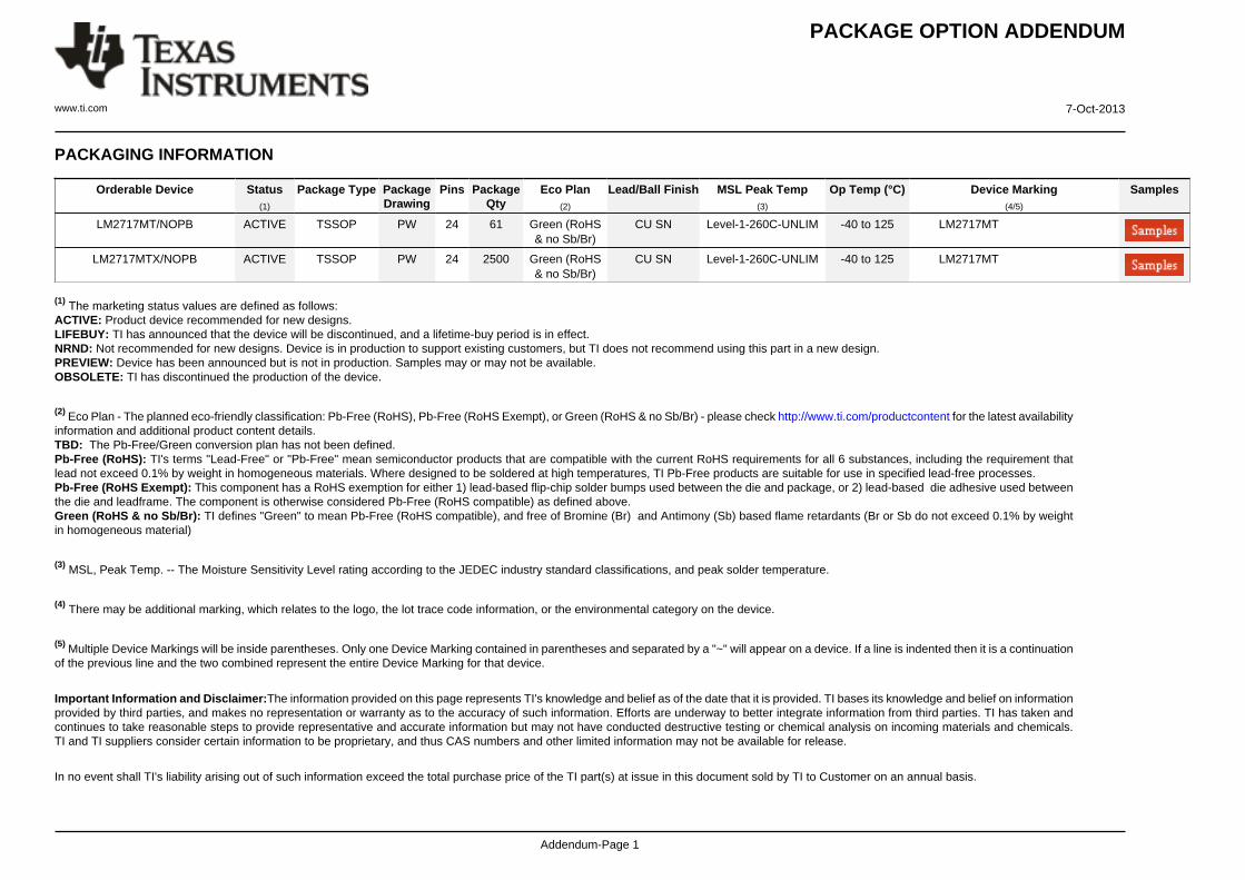
PACKAGING INFORMATION
Orderable Device Status(1)
Package Type PackageDrawing
Pins PackageQty
Eco Plan(2)
Lead/Ball Finish MSL Peak Temp(3)
Op Temp (°C) Device Marking(4/5)
Samples
LM2717MT/NOPB ACTIVE TSSOP PW 24 61 Green (RoHS& no Sb/Br)
CU SN Level-1-260C-UNLIM -40 to 125 LM2717MT
LM2717MTX/NOPB ACTIVE TSSOP PW 24 2500 Green (RoHS& no Sb/Br)
CU SN Level-1-260C-UNLIM -40 to 125 LM2717MT
(1) The marketing status values are defined as follows:ACTIVE: Product device recommended for new designs.LIFEBUY: TI has announced that the device will be discontinued, and a lifetime-buy period is in effect.NRND: Not recommended for new designs. Device is in production to support existing customers, but TI does not recommend using this part in a new design.PREVIEW: Device has been announced but is not in production. Samples may or may not be available.OBSOLETE: TI has discontinued the production of the device.
(2) Eco Plan - The planned eco-friendly classification: Pb-Free (RoHS), Pb-Free (RoHS Exempt), or Green (RoHS & no Sb/Br) - please check http://www.ti.com/productcontent for the latest availabilityinformation and additional product content details.TBD: The Pb-Free/Green conversion plan has not been defined.Pb-Free (RoHS): TI's terms "Lead-Free" or "Pb-Free" mean semiconductor products that are compatible with the current RoHS requirements for all 6 substances, including the requirement thatlead not exceed 0.1% by weight in homogeneous materials. Where designed to be soldered at high temperatures, TI Pb-Free products are suitable for use in specified lead-free processes.Pb-Free (RoHS Exempt): This component has a RoHS exemption for either 1) lead-based flip-chip solder bumps used between the die and package, or 2) lead-based die adhesive used betweenthe die and leadframe. The component is otherwise considered Pb-Free (RoHS compatible) as defined above.Green (RoHS & no Sb/Br): TI defines "Green" to mean Pb-Free (RoHS compatible), and free of Bromine (Br) and Antimony (Sb) based flame retardants (Br or Sb do not exceed 0.1% by weightin homogeneous material)
(3) MSL, Peak Temp. -- The Moisture Sensitivity Level rating according to the JEDEC industry standard classifications, and peak solder temperature.
(4) There may be additional marking, which relates to the logo, the lot trace code information, or the environmental category on the device.
(5) Multiple Device Markings will be inside parentheses. Only one Device Marking contained in parentheses and separated by a "~" will appear on a device. If a line is indented then it is a continuationof the previous line and the two combined represent the entire Device Marking for that device.
Important Information and Disclaimer:The information provided on this page represents TI's knowledge and belief as of the date that it is provided. TI bases its knowledge and belief on informationprovided by third parties, and makes no representation or warranty as to the accuracy of such information. Efforts are underway to better integrate information from third parties. TI has taken andcontinues to take reasonable steps to provide representative and accurate information but may not have conducted destructive testing or chemical analysis on incoming materials and chemicals.TI and TI suppliers consider certain information to be proprietary, and thus CAS numbers and other limited information may not be available for release.
In no event shall TI's liability arising out of such information exceed the total purchase price of the TI part(s) at issue in this document sold by TI to Customer on an annual basis.
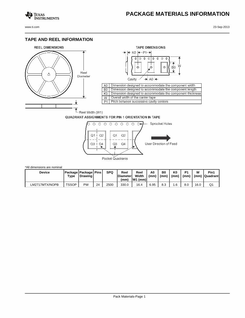
TAPE AND REEL INFORMATION
*All dimensions are nominal
Device PackageType
PackageDrawing
Pins SPQ ReelDiameter
(mm)
ReelWidth
W1 (mm)
A0(mm)
B0(mm)
K0(mm)
P1(mm)
W(mm)
Pin1Quadrant
LM2717MTX/NOPB TSSOP PW 24 2500 330.0 16.4 6.95 8.3 1.6 8.0 16.0 Q1
PACKAGE MATERIALS INFORMATION
www.ti.com 23-Sep-2013
Pack Materials-Page 1
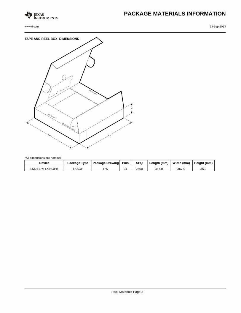
*All dimensions are nominal
Device Package Type Package Drawing Pins SPQ Length (mm) Width (mm) Height (mm)
LM2717MTX/NOPB TSSOP PW 24 2500 367.0 367.0 35.0
PACKAGE MATERIALS INFORMATION
www.ti.com 23-Sep-2013
Pack Materials-Page 2
IMPORTANT NOTICE
Texas Instruments Incorporated and its subsidiaries (TI) reserve the right to make corrections, enhancements, improvements and otherchanges to its semiconductor products and services per JESD46, latest issue, and to discontinue any product or service per JESD48, latestissue. Buyers should obtain the latest relevant information before placing orders and should verify that such information is current andcomplete. All semiconductor products (also referred to herein as “components”) are sold subject to TI’s terms and conditions of salesupplied at the time of order acknowledgment.TI warrants performance of its components to the specifications applicable at the time of sale, in accordance with the warranty in TI’s termsand conditions of sale of semiconductor products. Testing and other quality control techniques are used to the extent TI deems necessaryto support this warranty. Except where mandated by applicable law, testing of all parameters of each component is not necessarilyperformed.TI assumes no liability for applications assistance or the design of Buyers’ products. Buyers are responsible for their products andapplications using TI components. To minimize the risks associated with Buyers’ products and applications, Buyers should provideadequate design and operating safeguards.TI does not warrant or represent that any license, either express or implied, is granted under any patent right, copyright, mask work right, orother intellectual property right relating to any combination, machine, or process in which TI components or services are used. Informationpublished by TI regarding third-party products or services does not constitute a license to use such products or services or a warranty orendorsement thereof. Use of such information may require a license from a third party under the patents or other intellectual property of thethird party, or a license from TI under the patents or other intellectual property of TI.Reproduction of significant portions of TI information in TI data books or data sheets is permissible only if reproduction is without alterationand is accompanied by all associated warranties, conditions, limitations, and notices. TI is not responsible or liable for such altereddocumentation. Information of third parties may be subject to additional restrictions.Resale of TI components or services with statements different from or beyond the parameters stated by TI for that component or servicevoids all express and any implied warranties for the associated TI component or service and is an unfair and deceptive business practice.TI is not responsible or liable for any such statements.Buyer acknowledges and agrees that it is solely responsible for compliance with all legal, regulatory and safety-related requirementsconcerning its products, and any use of TI components in its applications, notwithstanding any applications-related information or supportthat may be provided by TI. Buyer represents and agrees that it has all the necessary expertise to create and implement safeguards whichanticipate dangerous consequences of failures, monitor failures and their consequences, lessen the likelihood of failures that might causeharm and take appropriate remedial actions. Buyer will fully indemnify TI and its representatives against any damages arising out of the useof any TI components in safety-critical applications.In some cases, TI components may be promoted specifically to facilitate safety-related applications. With such components, TI’s goal is tohelp enable customers to design and create their own end-product solutions that meet applicable functional safety standards andrequirements. Nonetheless, such components are subject to these terms.No TI components are authorized for use in FDA Class III (or similar life-critical medical equipment) unless authorized officers of the partieshave executed a special agreement specifically governing such use.Only those TI components which TI has specifically designated as military grade or “enhanced plastic” are designed and intended for use inmilitary/aerospace applications or environments. Buyer acknowledges and agrees that any military or aerospace use of TI componentswhich have not been so designated is solely at the Buyer's risk, and that Buyer is solely responsible for compliance with all legal andregulatory requirements in connection with such use.TI has specifically designated certain components as meeting ISO/TS16949 requirements, mainly for automotive use. In any case of use ofnon-designated products, TI will not be responsible for any failure to meet ISO/TS16949.
Products ApplicationsAudio www.ti.com/audio Automotive and Transportation www.ti.com/automotiveAmplifiers amplifier.ti.com Communications and Telecom www.ti.com/communicationsData Converters dataconverter.ti.com Computers and Peripherals www.ti.com/computersDLP® Products www.dlp.com Consumer Electronics www.ti.com/consumer-appsDSP dsp.ti.com Energy and Lighting www.ti.com/energyClocks and Timers www.ti.com/clocks Industrial www.ti.com/industrialInterface interface.ti.com Medical www.ti.com/medicalLogic logic.ti.com Security www.ti.com/securityPower Mgmt power.ti.com Space, Avionics and Defense www.ti.com/space-avionics-defenseMicrocontrollers microcontroller.ti.com Video and Imaging www.ti.com/videoRFID www.ti-rfid.comOMAP Applications Processors www.ti.com/omap TI E2E Community e2e.ti.comWireless Connectivity www.ti.com/wirelessconnectivity
Mailing Address: Texas Instruments, Post Office Box 655303, Dallas, Texas 75265Copyright © 2016, Texas Instruments Incorporated