R1243x Series - Mouser Electronics · R1243x Series 30 V Input 2 A Buck DC/DC Converter...
47
R1243x Series 30 V Input 2 A Buck DC/DC Converter NO.EA-206-180129 1 OUTLINE The R1243x is a CMOS-based step-down DC/DC converter with internal Nch high-side Tr. (0.175 Ω), which can provide the maximum 2 A output current. Internally, the R1243x consists of an oscillator, a PWM control circuit, a reference voltage unit, an error amplifier, phase compensation circuits, a slope circuit, a soft-start circuit, protection circuits, internal voltage regulators and a switch for bootstrap circuit. A step-down DC/DC converter can be configured by only adding an inductor, resistors, a diode and capacitors to the R1243x. The R1243x is a current mode operating type DC/DC converter that does not require external current sense resistor. It has high-speed response time and is high efficiency and compatible with ceramic capacitors. The oscillator frequency of the R1243x001A/B/E is fixed to 1000 kHz. The oscillator frequency of the R1243x001C/D is fixed 330 kHz. The R1243x has a cycle-by-cycle peak current limit function, a short protection function, a thermal shutdown function and an UVLO as protection features. The R1243x001A/C/E has a latch protection with 2 ms delay time, the R1243x001B/D has a fold-back protection that keep operating during short condition with lower operating frequency and limiting the LX current. The R1243x has a built-in soft-start time (Typ. 0.4 ms). In addition to this, the soft-start time is adjustable by adding an external capacitor. The R1243x has the FLG pin, which mainly monitors the FB pin voltage and gives a flag output by the Nch open drain if the abnormal condition is detected. The R1243x is offered in 8-pin HSOP-8E and 10-pin DFN(PLP)2527-10 packages that can achieve high density mounting. FEATURES • Operating Voltage Range ...................................... 4.5 V to 30 V • Standby Current..................................................... Max. 10 μA (VIN = 30 V, CE = L) • Supply Current ....................................................... Typ. 0.7 mA (VIN = 30 V, VFB = 1.0 V) • Output Voltage Range ........................................... 0.8 V to 18 V, Adjustable with external resistors • Feedback Voltage .................................................. 0.5 V with 1.4% accuracy • Output Current ....................................................... Max. 2 A (1) • Peak Current Limiting ............................................ Typ. 3.8 A • Internal Nch MOSFET Driver ................................. Typ. 175 mΩ • Maximum Duty Cycle ............................................. Min. 85% • Oscillator Frequency .............................................. R1243x001A/B/E: 1000 kHz, R1243x001C/D: 330 kHz • Latch Type Protection ............................................ R1243x001A/C: Typ. 2 ms, R1243x001E: 0.08 ms • Fold-back Type Protection ..................................... R1243x001B: 250 kHz, R1243x001D: 82.5 kH • Internal Soft-start Time .......................................... Typ. 0.4 ms, TSS = Open • External Soft-start Time ......................................... Typ. 12 ms, CSS = 0.1 μF • Flag Output ............................................................ Typ. 0.25 ms, FLG “OFF” delay time • UVLO Released Voltage ........................................ Typ. 4.0 V • Thermal Shutdown................................................. Typ. 160°C, Hysteresis = 35°C • Package ............................................................... HSOP-8E, DFN(PLP)2527-10 (1) This is an approximate value, because output current depends on conditions and external parts.
Transcript of R1243x Series - Mouser Electronics · R1243x Series 30 V Input 2 A Buck DC/DC Converter...
R1243x Series
30 V Input 2 A Buck DC/DC Converter
NO.EA-206-180129
1
OUTLINE The R1243x is a CMOS-based step-down DC/DC converter with internal Nch high-side Tr. (0.175 Ω), which can provide the maximum 2 A output current. Internally, the R1243x consists of an oscillator, a PWM control circuit, a reference voltage unit, an error amplifier, phase compensation circuits, a slope circuit, a soft-start circuit, protection circuits, internal voltage regulators and a switch for bootstrap circuit. A step-down DC/DC converter can be configured by only adding an inductor, resistors, a diode and capacitors to the R1243x. The R1243x is a current mode operating type DC/DC converter that does not require external current sense resistor. It has high-speed response time and is high efficiency and compatible with ceramic capacitors. The oscillator frequency of the R1243x001A/B/E is fixed to 1000 kHz. The oscillator frequency of the R1243x001C/D is fixed 330 kHz. The R1243x has a cycle-by-cycle peak current limit function, a short protection function, a thermal shutdown function and an UVLO as protection features. The R1243x001A/C/E has a latch protection with 2 ms delay time, the R1243x001B/D has a fold-back protection that keep operating during short condition with lower operating frequency and limiting the LX current. The R1243x has a built-in soft-start time (Typ. 0.4 ms). In addition to this, the soft-start time is adjustable by adding an external capacitor. The R1243x has the FLG pin, which mainly monitors the FB pin voltage and gives a flag output by the Nch open drain if the abnormal condition is detected. The R1243x is offered in 8-pin HSOP-8E and 10-pin DFN(PLP)2527-10 packages that can achieve high density mounting.
FEATURES • Operating Voltage Range ...................................... 4.5 V to 30 V • Standby Current..................................................... Max. 10 µA (VIN = 30 V, CE = L) • Supply Current ....................................................... Typ. 0.7 mA (VIN = 30 V, VFB = 1.0 V) • Output Voltage Range ........................................... 0.8 V to 18 V, Adjustable with external resistors • Feedback Voltage .................................................. 0.5 V with 1.4% accuracy • Output Current ....................................................... Max. 2 A(1) • Peak Current Limiting ............................................ Typ. 3.8 A • Internal Nch MOSFET Driver ................................. Typ. 175 mΩ • Maximum Duty Cycle ............................................. Min. 85% • Oscillator Frequency .............................................. R1243x001A/B/E: 1000 kHz, R1243x001C/D: 330 kHz • Latch Type Protection ............................................ R1243x001A/C: Typ. 2 ms, R1243x001E: 0.08 ms • Fold-back Type Protection ..................................... R1243x001B: 250 kHz, R1243x001D: 82.5 kH • Internal Soft-start Time .......................................... Typ. 0.4 ms, TSS = Open • External Soft-start Time ......................................... Typ. 12 ms, CSS = 0.1 µF • Flag Output ............................................................ Typ. 0.25 ms, FLG “OFF” delay time • UVLO Released Voltage ........................................ Typ. 4.0 V • Thermal Shutdown................................................. Typ. 160°C, Hysteresis = 35°C • Package ............................................................... HSOP-8E, DFN(PLP)2527-10 (1) This is an approximate value, because output current depends on conditions and external parts.
R1243x NO.EA-206-180129
2
APPLICATIONS • Digital Home Appliances • Hand-held Communication Equipment: Cameras, VCRs, Camcorders • Battery-powered Equipment • Battery Charger
SELECTION GUIDE The package type, the oscillator frequency (Fixed: 1000 kHz, 330 kHz) and the short-circuit protection type (Latch, Fold-back) are user-selectable options. Selection Guide
Product Name Package Quantity per Reel Pb Free Halogen Free R1243S001∗-E2-FE HSOP-8E 1,000 pcs Yes Yes R1243K001∗-TR DFN(PLP)2527-10 5,000 pcs Yes Yes ∗: Specify the oscillator frequency and the short-circuit protection type.
(A) Fixed Frequency: 1000 kHz, Latch Type (2 ms) (B) Fixed Frequency: 1000 kHz, Fold-back Type (C) Fixed Frequency: 330 kHz, Latch Type (2 ms) (D) Fixed Frequency: 330 kHz, Fold-back Type (E) Fixed Frequency: 1000 kHz, Latch Type (2 ms), only for HSOP-8E
R1243x NO.EA-206-180129
3
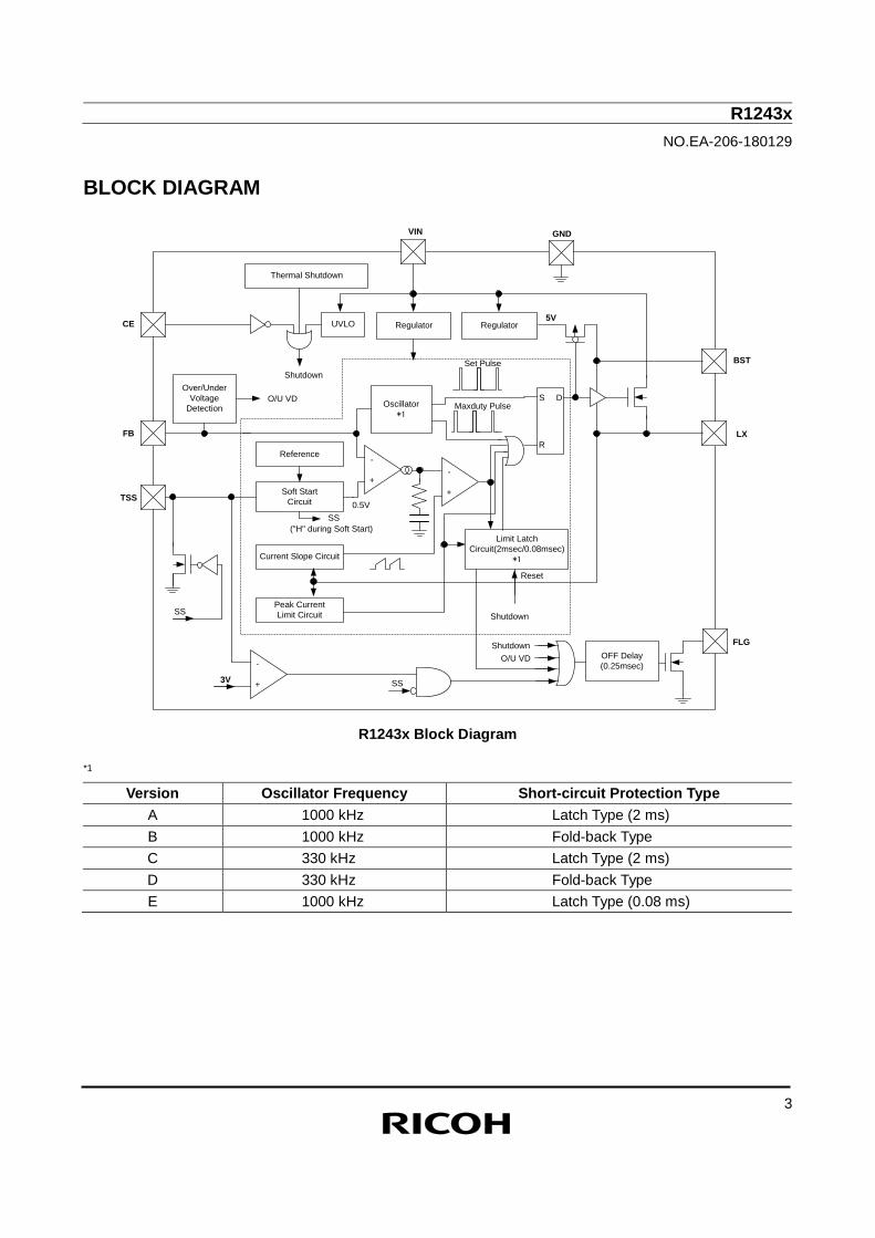
BLOCK DIAGRAM
FB
CE
-
+
Oscillator*1
Regulator5V
R
S D
Current Slope Circuit
Reference
Soft StartCircuit
-
+
UVLO
0.5V
Regulator
Thermal Shutdown
Peak Current Limit Circuit
VIN
Limit LatchCircuit(2msec/0.08msec)
*1
Shutdown
GND
FLG
BST
Over/Under Voltage
Detection
O/U VDShutdown
O/U VD
TSS
OFF Delay(0.25msec)-
+3V SS
Set Pulse
Maxduty Pulse
SS
LX
Reset
Shutdown
SS("H" during Soft Start)
R1243x Block Diagram *1
Version Oscillator Frequency Short-circuit Protection Type A 1000 kHz Latch Type (2 ms) B 1000 kHz Fold-back Type C 330 kHz Latch Type (2 ms) D 330 kHz Fold-back Type E 1000 kHz Latch Type (0.08 ms)
R1243x NO.EA-206-180129
4
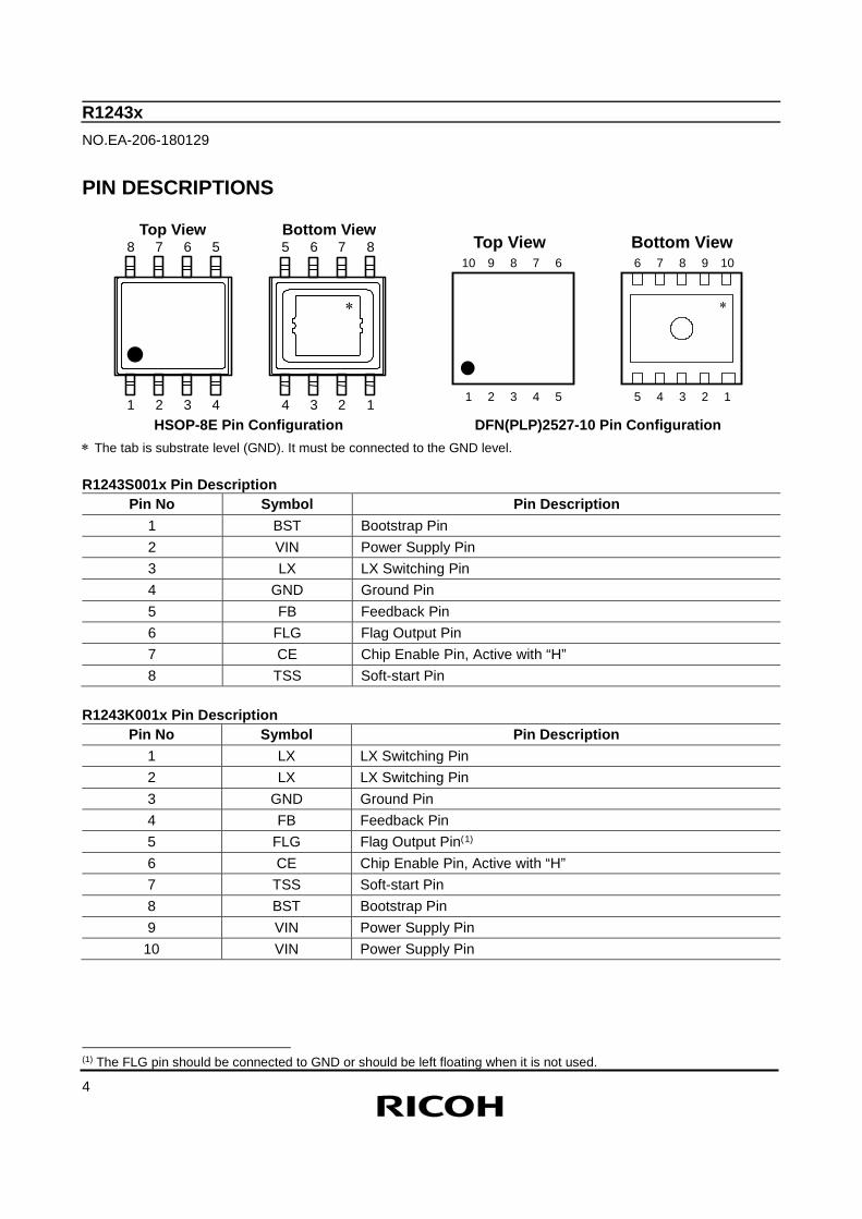
PIN DESCRIPTIONS
Top View Bottom View 5 8 6
4 2 1 3
8 6 5 7
1 3 4 2
7
∗
Bottom View Top View 6 10 7 8 9
5 1 4 3 2
10 6 9 8 7
1 5 2 3 4
∗
HSOP-8E Pin Configuration DFN(PLP)2527-10 Pin Configuration
∗ The tab is substrate level (GND). It must be connected to the GND level. R1243S001x Pin Description
Pin No Symbol Pin Description 1 BST Bootstrap Pin 2 VIN Power Supply Pin 3 LX LX Switching Pin 4 GND Ground Pin 5 FB Feedback Pin 6 FLG Flag Output Pin 7 CE Chip Enable Pin, Active with “H” 8 TSS Soft-start Pin
R1243K001x Pin Description
Pin No Symbol Pin Description 1 LX LX Switching Pin 2 LX LX Switching Pin 3 GND Ground Pin 4 FB Feedback Pin 5 FLG Flag Output Pin(1) 6 CE Chip Enable Pin, Active with “H” 7 TSS Soft-start Pin 8 BST Bootstrap Pin 9 VIN Power Supply Pin
10 VIN Power Supply Pin
(1) The FLG pin should be connected to GND or should be left floating when it is not used.
R1243x NO.EA-206-180129
5
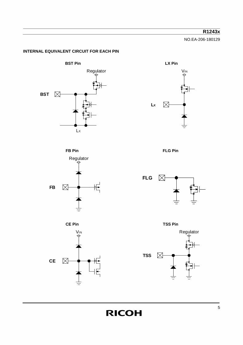
INTERNAL EQUIVALENT CIRCUIT FOR EACH PIN
BST Pin LX Pin
FB Pin FLG Pin
CE Pin TSS Pin
BST
LX
Regulator
LX
VIN
FB
Regulator
FLG
CE
VIN
TSS
Regulator
R1243x NO.EA-206-180129
6
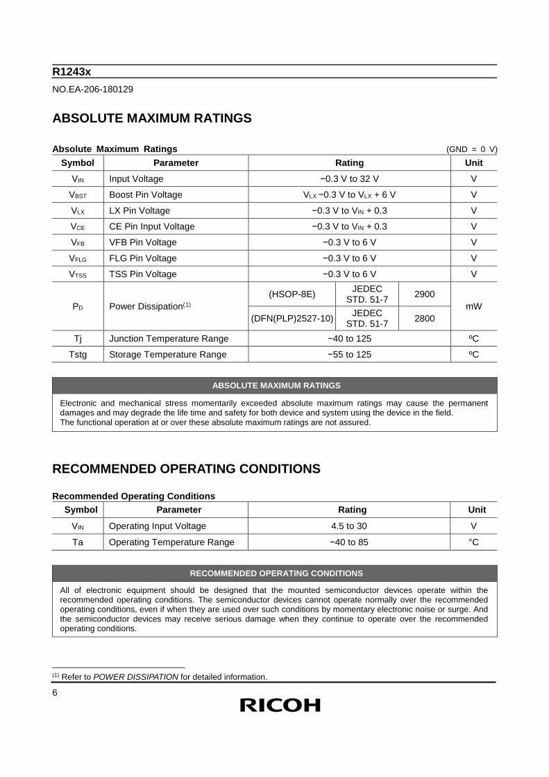
ABSOLUTE MAXIMUM RATINGS Absolute Maximum Ratings (GND = 0 V)
Symbol Parameter Rating Unit VIN Input Voltage −0.3 V to 32 V V
VBST Boost Pin Voltage VLX −0.3 V to VLX + 6 V V
VLX LX Pin Voltage −0.3 V to VIN + 0.3 V
VCE CE Pin Input Voltage −0.3 V to VIN + 0.3 V
VFB VFB Pin Voltage −0.3 V to 6 V V
VFLG FLG Pin Voltage −0.3 V to 6 V V
VTSS TSS Pin Voltage −0.3 V to 6 V V
PD Power Dissipation(1) (HSOP-8E) JEDEC
STD. 51-7 2900 mW
(DFN(PLP)2527-10) JEDEC STD. 51-7 2800
Tj Junction Temperature Range −40 to 125 ºC
Tstg Storage Temperature Range −55 to 125 ºC
ABSOLUTE MAXIMUM RATINGS
Electronic and mechanical stress momentarily exceeded absolute maximum ratings may cause the permanent damages and may degrade the life time and safety for both device and system using the device in the field. The functional operation at or over these absolute maximum ratings are not assured.
RECOMMENDED OPERATING CONDITIONS Recommended Operating Conditions
Symbol Parameter Rating Unit
VIN Operating Input Voltage 4.5 to 30 V
Ta Operating Temperature Range −40 to 85 °C
RECOMMENDED OPERATING CONDITIONS
All of electronic equipment should be designed that the mounted semiconductor devices operate within the recommended operating conditions. The semiconductor devices cannot operate normally over the recommended operating conditions, even if when they are used over such conditions by momentary electronic noise or surge. And the semiconductor devices may receive serious damage when they continue to operate over the recommended operating conditions.
(1) Refer to POWER DISSIPATION for detailed information.
R1243x NO.EA-206-180129
7
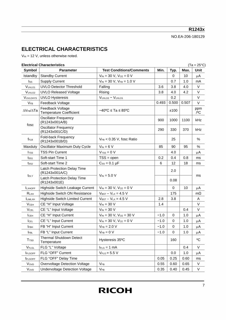
ELECTRICAL CHARACTERISTICS VIN = 12 V, unless otherwise noted. Electrical Characteristics (Ta = 25°C)
Symbol Parameter Test Conditions/Comments Min. Typ. Max. Unit Istandby Standby Current VIN = 30 V, VCE = 0 V 0 10 µA
ISS Supply Current VIN = 30 V, VFB = 1.0 V 0.7 1.0 mA VUVLO1 UVLO Detector Threshold Falling 3.6 3.8 4.0 V VUVLO2 UVLO Released Voltage Rising 3.8 4.0 4.2 V
VUVLOHYS UVLO Hysteresis VUVLO2 − VUVLO1 0.2 V VFB Feedback Voltage 0.493 0.500 0.507 V
∆VFB/∆Ta Feedback Voltage Temperature Coefficient −40ºC ≤ Ta ≤ 85ºC ±100 ppm
/ºC
fosc
Oscillator Frequency (R1243x001A/B) 900 1000 1100 kHz
Oscillator Frequency (R1243x001C/D) 290 330 370 kHz
fFLB Fold-back Frequency (R1243x001B/D) VFB < 0.35 V, fosc Ratio 25 %
Maxduty Oscillator Maximum Duty Cycle VIN = 6 V 85 90 95 % ITSS TSS Pin Current VTSS = 0 V 4.0 µA tSS1 Soft-start Time 1 TSS = open 0.2 0.4 0.8 ms tSS2 Soft-start Time 2 CSS = 0.1 µF 6 12 18 ms
tDLY
Latch Protection Delay Time (R1243x001A/C)
VIN = 5.0 V 2.0
ms Latch Protection Delay Time (R1243x001E) 0.08
ILXHOFF Highside Switch Leakage Current VIN = 30 V, VCE = 0 V 0 10 µA RLXH Highside Switch ON Resistance VBST – VLX = 4.5 V 175 mΩ
ILIMLXH Highside Switch Limited Current VBST – VLX = 4.5 V 2.8 3.8 A VCEH CE “H” Input Voltage VIN = 30 V 1.4 V VCEL CE “L” Input Voltage VIN = 30 V 0.4 V ICEH CE “H” Input Current VIN = 30 V, VCE = 30 V −1.0 0 1.0 µA ICEL CE “L” Input Current VIN = 30 V, VCE = 0 V −1.0 0 1.0 µA IFBH FB “H” Input Current VFB = 2.0 V −1.0 0 1.0 µA IFBL FB “L” Input Current VFB = 0 V −1.0 0 1.0 µA
TTSD Thermal Shutdown Detect Temperature Hysteresis 35ºC 160 ºC
VFLGL FLG “L” Voltage IFLG = 1 mA 0.4 V IFLGOFF FLG “OFF” Current VFLG = 5.5 V 0.0 1.0 µA tFLGOFF FLG “OFF” Delay Time 0.05 0.25 0.60 ms VOVD Overvoltage Detection Voltage VFB 0.55 0.60 0.65 V VUVD Undervoltage Detection Voltage VFB 0.35 0.40 0.45 V
R1243x NO.EA-206-180129
8
OPERATING DESCRIPTIONS
SOFT-START TIME ADJUSTMENT FUNCTION AND FLAG FUNCTION
Soft-Start Time Adjustment Function
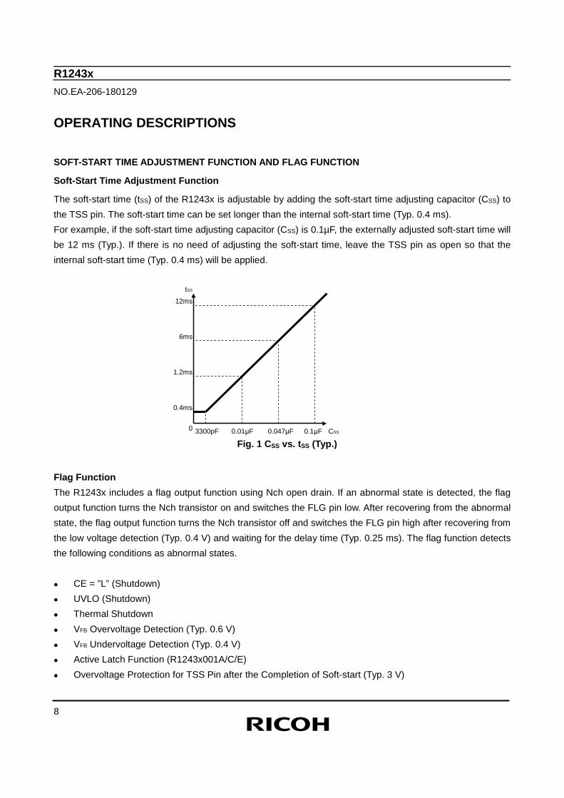
The soft-start time (tSS) of the R1243x is adjustable by adding the soft-start time adjusting capacitor (CSS) to the TSS pin. The soft-start time can be set longer than the internal soft-start time (Typ. 0.4 ms). For example, if the soft-start time adjusting capacitor (CSS) is 0.1µF, the externally adjusted soft-start time will be 12 ms (Typ.). If there is no need of adjusting the soft-start time, leave the TSS pin as open so that the internal soft-start time (Typ. 0.4 ms) will be applied.
Fig. 1 CSS vs. tSS (Typ.)
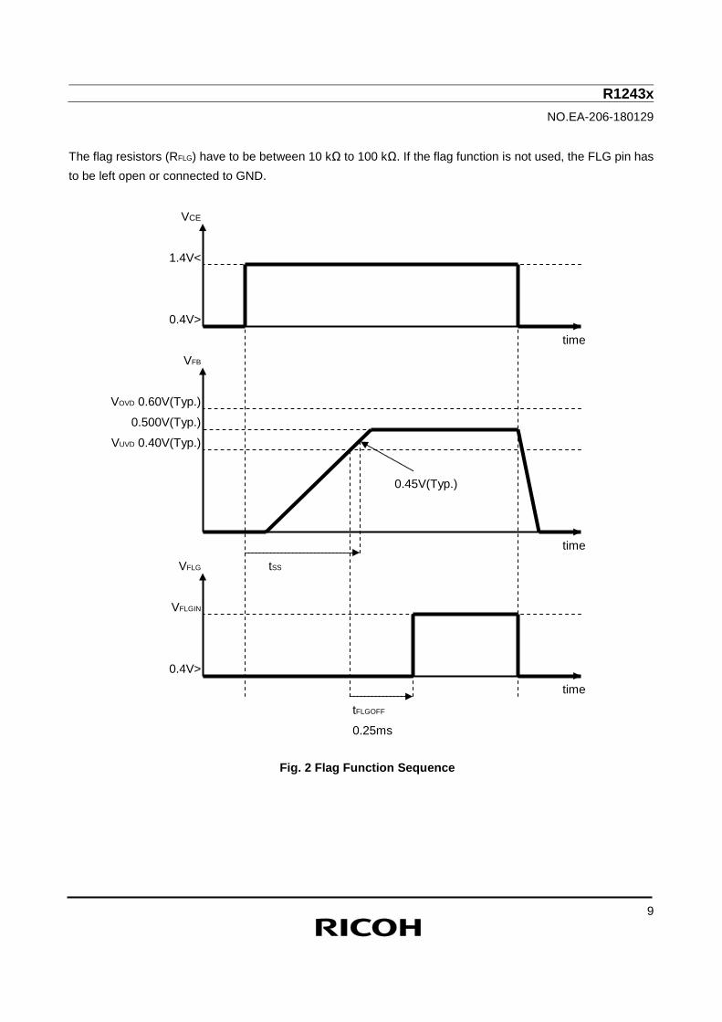
Flag Function The R1243x includes a flag output function using Nch open drain. If an abnormal state is detected, the flag output function turns the Nch transistor on and switches the FLG pin low. After recovering from the abnormal state, the flag output function turns the Nch transistor off and switches the FLG pin high after recovering from the low voltage detection (Typ. 0.4 V) and waiting for the delay time (Typ. 0.25 ms). The flag function detects the following conditions as abnormal states. CE = ”L” (Shutdown) UVLO (Shutdown) Thermal Shutdown VFB Overvoltage Detection (Typ. 0.6 V) VFB Undervoltage Detection (Typ. 0.4 V) Active Latch Function (R1243x001A/C/E) Overvoltage Protection for TSS Pin after the Completion of Soft-start (Typ. 3 V)
tSS
12ms
6ms
1.2ms
0.4ms
0 3300pF 0.01μF 0.047μF 0.1μF CSS
R1243x NO.EA-206-180129
9
The flag resistors (RFLG) have to be between 10 kΩ to 100 kΩ. If the flag function is not used, the FLG pin has to be left open or connected to GND.
Fig. 2 Flag Function Sequence
VCE
1.4V<
0.4V>
time
VFB
VOVD 0.60V(Typ.)
0.500V(Typ.)
VUVD 0.40V(Typ.)
0.45V(Typ.)
time
VFLG tSS
VFLGIN
0.4V>
time
tFLGOFF
0.25ms
R1243x NO.EA-206-180129
10
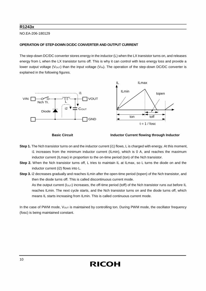
OPERATION OF STEP-DOWN DC/DC CONVERTER AND OUTPUT CURRENT The step-down DC/DC converter stores energy in the inductor (L) when the LX transistor turns on, and releases energy from L when the LX transistor turns off. This is why it can control with less energy loss and provide a lower output voltage (VOUT) than the input voltage (VIN). The operation of the step-down DC/DC converter is explained in the following figures.
Nch Tr. L
Diode
VIN
i1
VOUT
COUT i2
GND
Basic Circuit Inductor Current flowing through Inductor Step 1. The Nch transistor turns on and the inductor current (i1) flows, L is charged with energy. At this moment,
i1 increases from the minimum inductor current (ILmin), which is 0 A, and reaches the maximum inductor current (ILmax) in proportion to the on-time period (ton) of the Nch transistor.
Step 2. When the Nch transistor turns off, L tries to maintain IL at ILmax, so L turns the diode on and the inductor current (i2) flows into L.
Step 3. i2 decreases gradually and reaches ILmin after the open-time period (topen) of the Nch transistor, and then the diode turns off. This is called discontinuous current mode. As the output current (IOUT) increases, the off-time period (toff) of the Nch transistor runs out before IL reaches ILmin. The next cycle starts, and the Nch transistor turns on and the diode turns off, which means IL starts increasing from ILmin. This is called continuous current mode.
In the case of PWM mode, VOUT is maintained by controlling ton. During PWM mode, the oscillator frequency (fosc) is being maintained constant.
t = 1 / fosc
toff
topen ILmin
ILmax
ton
IL
R1243x NO.EA-206-180129
11
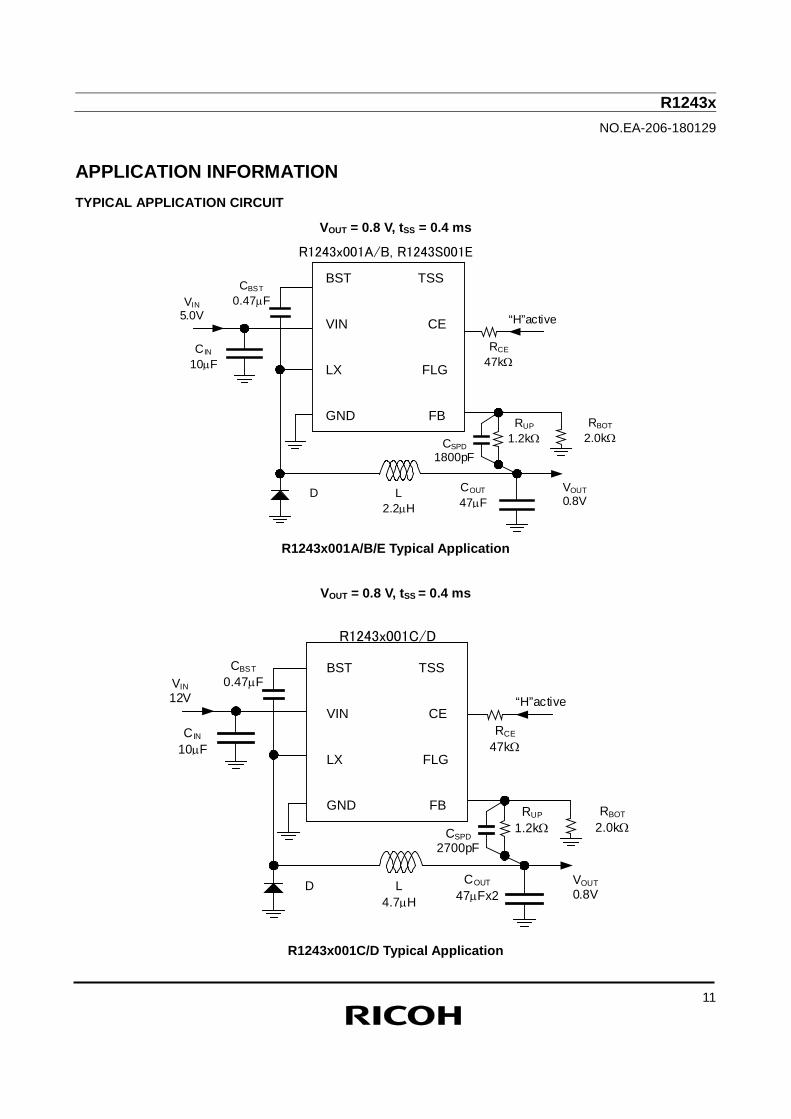
APPLICATION INFORMATION TYPICAL APPLICATION CIRCUIT
VOUT = 0.8 V, tSS = 0.4 ms
R1243x001A/B/E Typical Application
VOUT = 0.8 V, tSS = 0.4 ms
R1243x001C/D Typical Application
CBST 0.47µF
CIN 10µF
VIN 5.0V
RCE 47kΩ
“H”active
L 2.2µH
COUT 47µF
VOUT 0.8V
RUP 1.2kΩ
RBOT 2.0kΩ
D
CSPD 1800pF
GND
Lx
VIN
BST
FB
FLG
CE
TSS
R1243x001A/B, R1243S001E
CBST 0.47µF
CIN 10µF
VIN 12V
RCE 47kΩ
“H”active
L 4.7µH
COUT 47µFx2
VOUT 0.8V
RUP 1.2kΩ
RBOT 2.0kΩ
D
CSPD 2700pF
GND
Lx
VIN
BST
FB
FLG
CE
TSS
R1243x001C/D
BST TSS VIN CE LX FLG GND FB
BST TSS VIN CE LX FLG GND FB
R1243x NO.EA-206-180129
12
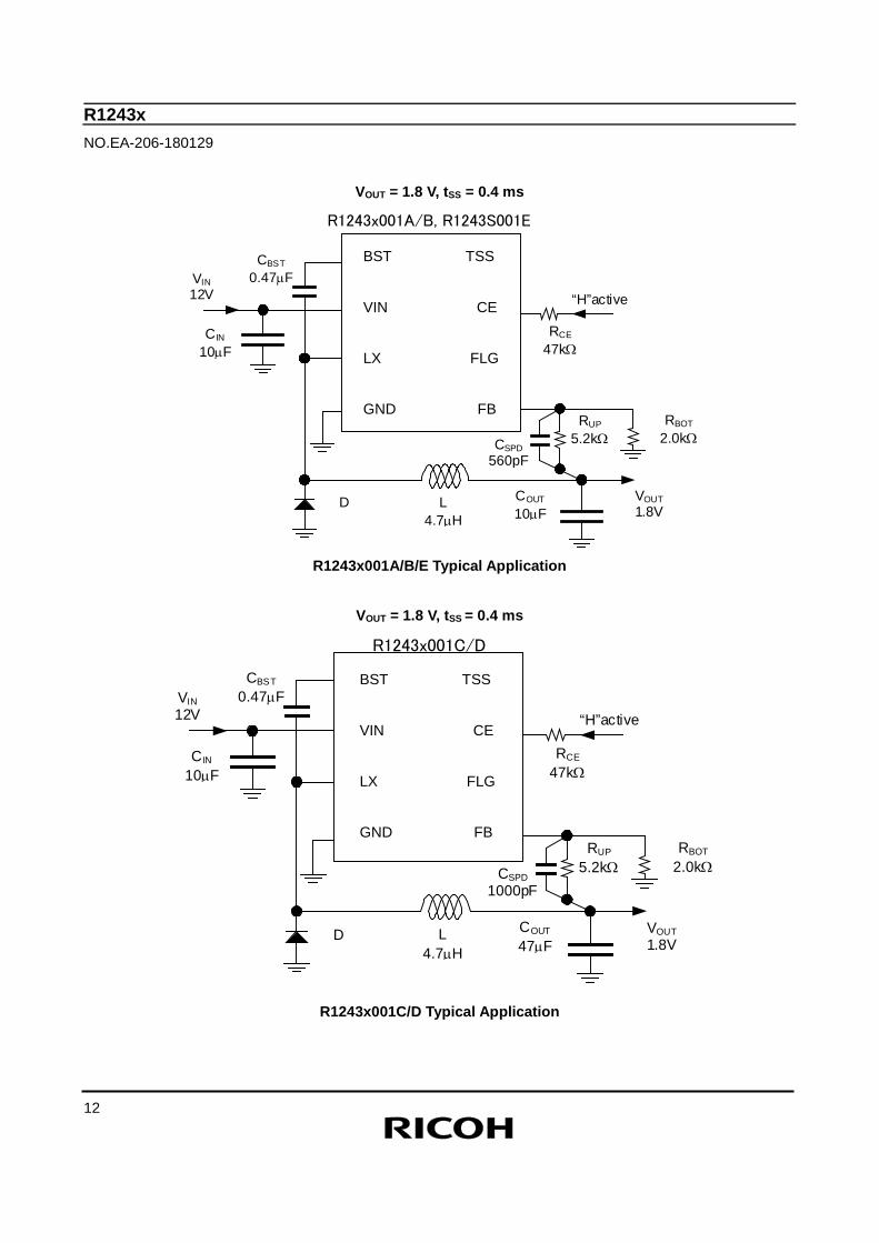
VOUT = 1.8 V, tSS = 0.4 ms
R1243x001A/B/E Typical Application
VOUT = 1.8 V, tSS = 0.4 ms
R1243x001C/D Typical Application
CBST 0.47µF
CIN 10µF
VIN 12V
RCE 47kΩ
“H”active
L 4.7µH
COUT 10µF
VOUT 1.8V
RUP 5.2kΩ
RBOT 2.0kΩ
D
CSPD 560pF
GND
Lx
VIN
BST
FB
FLG
CE
TSS
R1243x001A/B, R1243S001E
CBST 0.47µF
CIN 10µF
VIN 12V
RCE 47kΩ
“H”active
L 4.7µH
COUT 47µF
VOUT 1.8V
RUP 5.2kΩ
RBOT 2.0kΩ
D
CSPD 1000pF
GND
Lx
VIN
BST
FB
FLG
CE
TSS
R1243x001C/D
BST TSS VIN CE LX FLG GND FB
BST TSS VIN CE LX FLG GND FB
R1243x NO.EA-206-180129
13
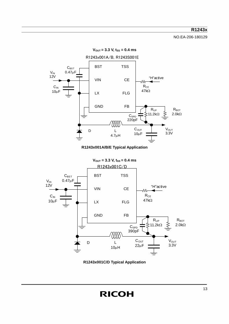
VOUT = 3.3 V, tSS = 0.4 ms
R1243x001A/B/E Typical Application
VOUT = 3.3 V, tSS = 0.4 ms
R1243x001C/D Typical Application
CBST 0.47µF
CIN 10µF
VIN 12V
RCE 47kΩ
“H”active
L 4.7µH
COUT 10µF
VOUT 3.3V
RUP 11.2kΩ
RBOT 2.0kΩ
D
CSPD 220pF
GND
Lx
VIN
BST
FB
FLG
CE
TSS
R1243x001A/B, R1243S001E
CBST 0.47µF
CIN 10µF
VIN 12V
RCE 47kΩ
“H”active
L 10µH
COUT 22µF
VOUT 3.3V
RUP 11.2kΩ
RBOT 2.0kΩ
D
CSPD 390pF
GND
Lx
VIN
BST
FB
FLG
CE
TSS
R1243x001C/D
BST TSS VIN CE LX FLG GND FB
BST TSS VIN CE LX FLG GND FB
R1243x NO.EA-206-180129
14
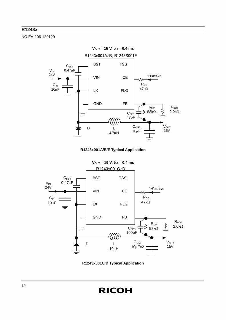
VOUT = 15 V, tSS = 0.4 ms
R1243x001A/B/E Typical Application
VOUT = 15 V, tSS = 0.4 ms
R1243x001C/D Typical Application
CBST 0.47µF
CIN 10µF
VIN 24V
RCE 47kΩ
“H”active
L 4.7µH
COUT 10µF
VOUT 15V
RUP 58kΩ
RBOT 2.0kΩ
D
CSPD 47pF
GND
Lx
VIN
BST
FB
FLG
CE
TSS
R1243x001A/B, R1243S001E
CBST 0.47µF
CIN 10µF
VIN 24V
RCE 47kΩ
“H”active
L 10µH
COUT 10µFx2
VOUT 15V
RUP 58kΩ
RBOT 2.0kΩ
D
CSPD 100pF
GND
Lx
VIN
BST
FB
FLG
CE
TSS
R1243x001C/D
BST TSS VIN CE LX FLG GND FB
BST TSS VIN CE LX FLG GND FB
R1243x NO.EA-206-180129
15
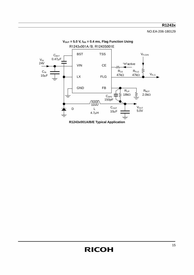
VOUT = 5.0 V, tSS = 0.4 ms, Flag Function Using
R1243x001A/B/E Typical Application
CBST 0.47µF
CIN 10µF
VIN 24V
RCE 47kΩ
“H”active
L 4.7µH
COUT 10µF
VOUT 5.0V
RUP 18kΩ
RBOT 2.0kΩ
D
RFLG 47kΩ VFLG
VFLGIN
CSPD 150pF
GND
Lx
VIN
BST
FB
FLG
CE
TSS
R1243x001A/B, R1243S001E
BST TSS VIN CE LX FLG GND FB
R1243x NO.EA-206-180129
16
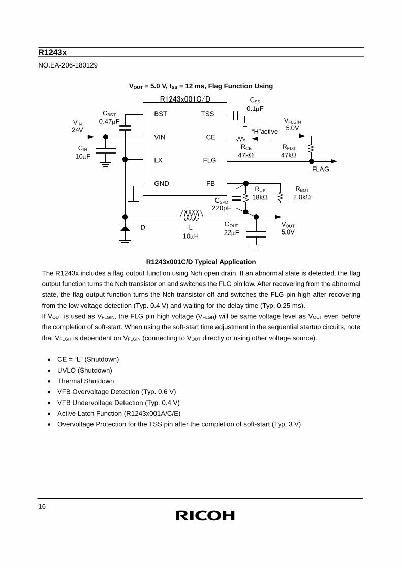
VOUT = 5.0 V, tSS = 12 ms, Flag Function Using
R1243x001C/D Typical Application
The R1243x includes a flag output function using Nch open drain. If an abnormal state is detected, the flag output function turns the Nch transistor on and switches the FLG pin low. After recovering from the abnormal state, the flag output function turns the Nch transistor off and switches the FLG pin high after recovering from the low voltage detection (Typ. 0.4 V) and waiting for the delay time (Typ. 0.25 ms). If VOUT is used as VFLGIN, the FLG pin high voltage (VFLGH) will be same voltage level as VOUT even before the completion of soft-start. When using the soft-start time adjustment in the sequential startup circuits, note that VFLGH is dependent on VFLGIN (connecting to VOUT directly or using other voltage source).
• CE = “L” (Shutdown) • UVLO (Shutdown) • Thermal Shutdown • VFB Overvoltage Detection (Typ. 0.6 V) • VFB Undervoltage Detection (Typ. 0.4 V) • Active Latch Function (R1243x001A/C/E) • Overvoltage Protection for the TSS pin after the completion of soft-start (Typ. 3 V)
CBST 0.47µF
CIN 10µF
VIN 24V
CSS 0.1µF
VFLGIN 5.0V
RCE 47kΩ
“H”active
RFLG 47kΩ
FLAG
L 10µH
COUT 22µF
VOUT 5.0V
RUP 18kΩ
RBOT 2.0kΩ
GND
Lx
VIN
BST
FB
FLG
CE
TSS
R1243x001C/D
D
CSPD 220pF
BST TSS VIN CE LX FLG GND FB
R1243x NO.EA-206-180129
17
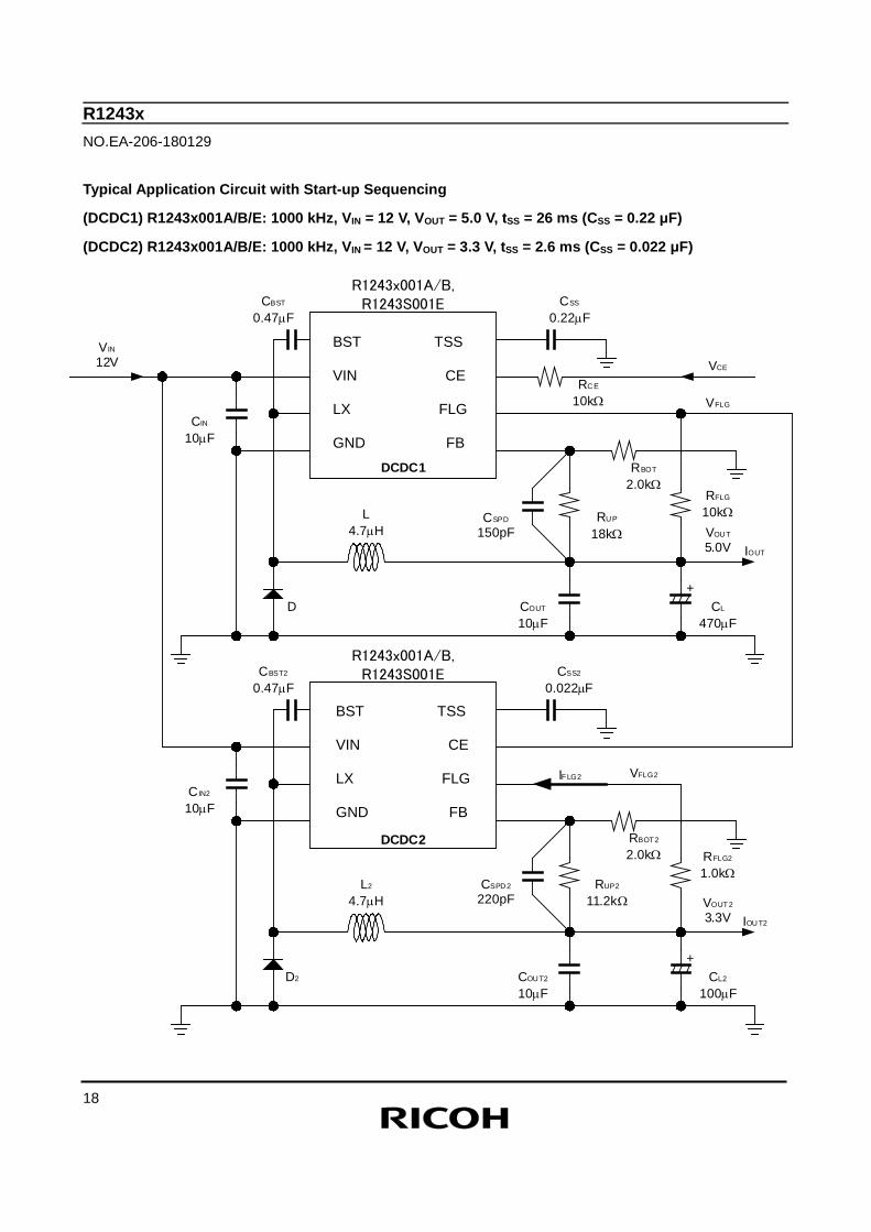
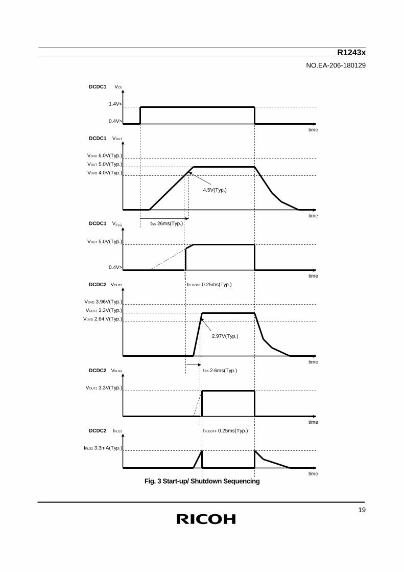
SEQUENTIAL START-UP The figure below shows the example of sequential startup circuits using soft-start time adjustment and flag functions. Where: the input voltage is 12 V, the output voltage of the R1243x001A/B/E (DCDC1) is 5.0 V, the output voltage of the R1243x001A/B/E (DCDC2) is 3.3 V, the electrolytic capacitor for the 5.0 V output is 470 µF and the electrolytic capacitor for the 3.3 V output is 100 µF. The DCDC1 circuit starts up first followed by the DCDC2 circuit, so that the output voltage of DCDC1 will not drop below the output voltage of the DCDC2. Soft-start Time and Charging Current During the soft-start, the R1243x generates a charging current (ICHRG) for a capacitor connected to VOUT in addition to the output current (IOUT) for supplying the output load. Therefore, IOUT is given by: IOUT’ = IOUT + ICHRG = IOUT + VOUT x (COUT + CL) / tSS IOUT2’ (DCDC1) and IOUT2’ (DCDC2) are given by: DCDC1: IOUT’ = IOUT + VOUT / (COUT + CL) / tSS = IOUT + 5.0 V x (10 μF + 470 μF) / 26 ms = IOUT + 92 mA DCDC2: IOUT2’ = IOUT2 + VOUT2 / (COUT2 + CL2) / tSS = IOUT + 3.3 V x (10 μF + 100 μF) / 2.6 ms = IOUT2 + 140 mA The output current should not exceed 2.0 A even during soft-start. Using the Output Voltage of DCDC1 as the FLG Pin Voltage of DCDC1 The R1243x includes a flag output function using Nch open drain. If an abnormal condition is detected, the flag output function turns the Nch transistor on and switches the FLG pin low. If an abnormal condition is not detected, the flag output function turns the Nch transistor off and switches the FLG pin high after recovering from the low voltage detection (Min. 0.35 V) and waiting for the delay time (Min. 0.05 ms). If VOUT is used as VFLGIN, the FLG pin high voltage (VFLGH) will be same voltage level as VOUT even before finishing the soft-start. After recovering from the low voltage detection, the lowest VFLGH will be 70% of the set output voltage (VSET). Using the FLG Pin Voltage of DCDC1 as the CE Pin Input Voltage of DCDC2 The lowest CE pin low voltage (VCEL) is 0.4 V, and the highest CE pin high voltage (VCEH) is 1.4 V. The highest flag pin low voltage (VFLGL) is 0.4 V and the lowest VFLGH of DCDC1 is approximately 3.5 V, so the flag pin voltage (VFLG) can be used as the CE pin input voltage (VCE) of DCDC2. Auto-discharge using the FLG Pin The R1243x turns the Nch transistor on and switches the FLG pin low during shutdown. If the FLG pin is switched low, a FLG pin current (IFLG) flows from VFLGIN to the FLG pin resistor (RFLG) and the Nch transistor. Therefore, using VOUT as VFLGIN can discharge the electric charges of a capacitor connected to VOUT during shutdown. The highest IFLG will be VFLGIN divided by RFLG. When determining the RFLG value, ensure that the highest IFLG
will be 5 mA or less. Do not directly connect VOUT to the FLG pin. IFLG may become excessive and damage the device. VFLGL is regulated as IFLG = 1 mA. If RFLG is set higher than IFLG = 1 mA, the highest VFLGL of 0.4 V is not guaranteed, hence the flag function itself may be spoiled.
R1243x NO.EA-206-180129
18
Typical Application Circuit with Start-up Sequencing
(DCDC1) R1243x001A/B/E: 1000 kHz, VIN = 12 V, VOUT = 5.0 V, tSS = 26 ms (CSS = 0.22 μF)
(DCDC2) R1243x001A/B/E: 1000 kHz, VIN = 12 V, VOUT = 3.3 V, tSS = 2.6 ms (CSS = 0.022 μF)
CBST 0.47µF
CIN 10µF
VIN 12V
CSS 0.22µF
L 4.7µH
COUT 10µF
VOU T 5.0V
RUP 18kΩ
RBOT 2.0kΩ
D
CSPD 150pF
GND
Lx
VIN
BST
FB
FLG
CE
TSS
R1243x001A/B,R1243S001E
RFLG 10kΩ
RC E 10kΩ
CBST2 0.47µF
CIN2 10µF
CSS2 0.022µF
L2 4.7µH
COU T2 10µF
VOUT2 3.3V
RUP2 11.2kΩ
RBOT2 2.0kΩ
D2
CSPD 2 220pF
GND
Lx
VIN
BST
FB
FLG
CE
TSS
R1243x001A/B,R1243S001E
RFLG2 1.0kΩ
CL 470µF
CL2 100µF
VCE
VFLG
VFLG2 IFLG2
DCDC1
DCDC2
+
+
IOUT
IOU T2
BST TSS VIN CE LX FLG GND FB
BST TSS VIN CE LX FLG GND FB
R1243x NO.EA-206-180129
19
Fig. 3 Start-up/ Shutdown Sequencing
DCDC1 VCE
1.4V<
0.4V>
time
DCDC1 VOUT
VOVD 6.0V(Typ.)
VOUT 5.0V(Typ.)
VUVD 4.0V(Typ.)
4.5V(Typ.)
timeDCDC1 VFLG tSS 26ms(Typ.)
VOUT 5.0V(Typ.)
0.4V>
time
DCDC2 VOUT2 tFLGOFF 0.25ms(Typ.)
VOVD 3.96V(Typ.)
VOUT2 3.3V(Typ.)
VUVD 2.64.V(Typ.)
2.97V(Typ.)
time
DCDC2 VFLG2 tSS 2.6ms(Typ.)
VOUT2 3.3V(Typ.)
time
DCDC2 IFLG2 tFLGOFF 0.25ms(Typ.)
IFLG2 3.3mA(Typ.)
time
R1243x NO.EA-206-180129
20
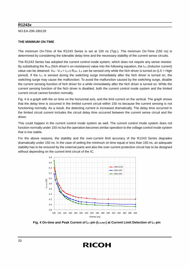
THE MINIMUM ON-TIME The minimum On-Time of the R1243 Series is set at 150 ns (Typ.). The minimum On-Time (150 ns) is determined by considering the tolerable delay time and the necessary stability of the current sense circuits.
The R1243 Series has adopted the current control mode system, which does not require any sense resistor. By substituting the RON (Nch driver's on-resistance) value into the following equation, the ILX (Inductor current) value can be obtained: VIN - VLX = ILX x RON. ILX can be sensed only while the Nch driver is turned on (LX = High period). If the ILX is sensed during the switching surge immediately after the Nch driver is turned on, the switching surge may cause the malfunction. To avoid the malfunction caused by the switching surge, disable the current sensing function of Nch driver for a while immediately after the Nch driver is turned on. While the current sensing function of the Nch driver is disabled, both the current control mode system and the limited current circuit cannot function normally.
Fig. 4 is a graph with the on time on the horizontal axis, and the limit current on the vertical. The graph shows that the delay time is occurred in the limited current circuit within 150 ns because the current sensing is not functioning normally. As a result, the detecting current is increased dramatically. The delay time occurred in the limited circuit current includes the circuit delay time occurred between the current sense circuit and the driver.
This could happen in the current control mode system as well. The current control mode system does not function normally under 150 ns but the operation becomes similar operation to the voltage control mode system that is low stable.
For the above reasons, the stability and the over-current limit accuracy of the R1243 Series degrades dramatically under 150 ns. In the case of setting the minimum on time equal or less than 150 ns, an adequate stability has to be ensured by the external parts and also the over current protection circuit has to be designed without depending on the current limit circuit of the IC.
Fig. 4 On-time and Peak Current of LX pin (ILXLIMIT) at Current Limit Detection of LX pin
3.8
4.0
4.2
4.4
4.6
4.8
5.0
5.2
5.4
5.6
5.8
100 120 140 160 180 200 220 240 260 280 300 320 340 360 380 400
Ontime [ns]
I LXLI
MIT
[A]
VIN=5.0VVIN=12VVIN=24V
R1243x NO.EA-206-180129
21
OUTPUT CURRENT AND SELECTION OF EXTERNAL COMPONENTS The following equations explain the relationship between output current and peripheral components. IRP is the ripple current P-P value, RONH is the ON resistance of Highside Tr., RL is the DC resistance of inductor. First, when Highside Tr. is “ON”, the following equation is satisfied. VIN = VOUT + (RONH + RL) × IOUT + L × IRP / ton ................................................................................ Equation 1 Second, when Highside Tr. is "OFF" (Diode is "ON"), the following equation is satisfied. L × IRP / toff = VF + VOUT + RL × IOUT ............................................................................................... Equation 2 Put Equation 2 to Equation 1 to solve ON duty of Highside Tr. (DON = ton / (toff + ton): DON = (VOUT + VF + RL × IOUT) / (VIN + VF - RONH × IOUT) .................................................................. Equation 3 Ripple Current is given by: IRP = (VIN - VOUT - RONH × IOUT - RL × IOUT) × DON / fosc / L .............................................................. Equation 4 Peak current (ILmax) that flows through L, and LX Tr. is given by: ILmax = IOUT + IRP / 2 ...................................................................................................................... Equation 5 The valley current (ILmin) is given by: ILmin = IOUT - IRP / 2 ....................................................................................................................... Equation 6 If ILmin is smaller than 0 (ILmin < 0), the step-down DC/DC converter operate in discontinuous mode. The step--down DC/DC converter operates in discontinuous mode when: IOUT < IRP / 2 .................................................................................................................................... Equation 7 It is important to consider ILmax and ILmin when making the input/output conditions or selecting the external components. The above explanation is based on the ideal operation of continuous mode.
R1243x NO.EA-206-180129
22
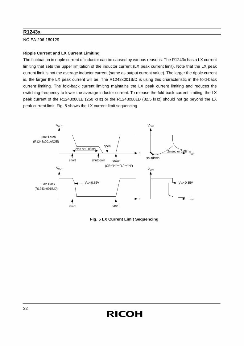
Ripple Current and LX Current Limiting The fluctuation in ripple current of inductor can be caused by various reasons. The R1243x has a LX current limiting that sets the upper limitation of the inductor current (LX peak current limit). Note that the LX peak current limit is not the average inductor current (same as output current value). The larger the ripple current is, the larger the LX peak current will be. The R1243x001B/D is using this characteristic in the fold-back current limiting. The fold-back current limiting maintains the LX peak current limiting and reduces the switching frequency to lower the average inductor current. To release the fold-back current limiting, the LX peak current of the R1243x001B (250 kHz) or the R1243x001D (82.5 kHz) should not go beyond the LX peak current limit. Fig. 5 shows the LX current limit sequencing.
Fig. 5 LX Current Limit Sequencing
t
t
VOUT
VOUT
short
2ms or 0.08ms
shutdown restart(CE="H"→"L"→"H")
short
open
open
VFB<0.35V
VOUT
IOUT
VOUT
IOUT
VFB<0.35V
Limit Latch(R1243x001A/C/E)
Fold Back(R1243x001B/D)
shutdown
2msec or 0.08ms
R1243x NO.EA-206-180129
23
Latch Protection for the R1243x001A/C/E After current limit detection, if a voltage drop continues more than a specified time, the R1243x001A/C/E enables a latch protection to turn off output. Note that if a power voltage rising is slow and the output voltage after soft-start is less than a set output voltage for more than a latch timer period. Refer to TECHNICAL NOTES for details. Fold-back Protection for the R1243x001B/D The R1243x00B/D enables a fold-back protection after soft-start. The fold-back protection reduces the oscillator frequency to 1/4 if the output voltage drops to 70% (Typ.) or less of a set output voltage, which means the FB pin voltage is typically 0.35 V or less. If an oscillator frequency decreases, a ripple current increases. As shown in Equation 8, with LX current limiting, the average current decreases as the ripple current increases. IOUT = ILmax − IRP / 2………………………………………………………………………………………Equation 8 Once the fold-back protection is enabled during heavy load, the R1243x may not be able to return to normal operation due to the increased ripple current. Note that if a power voltage rising is slow and the output voltage drops 70% (typ.) or less of a set output voltage after soft-start. Refer to TECHNICAL NOTES for details.
R1243x NO.EA-206-180129
24
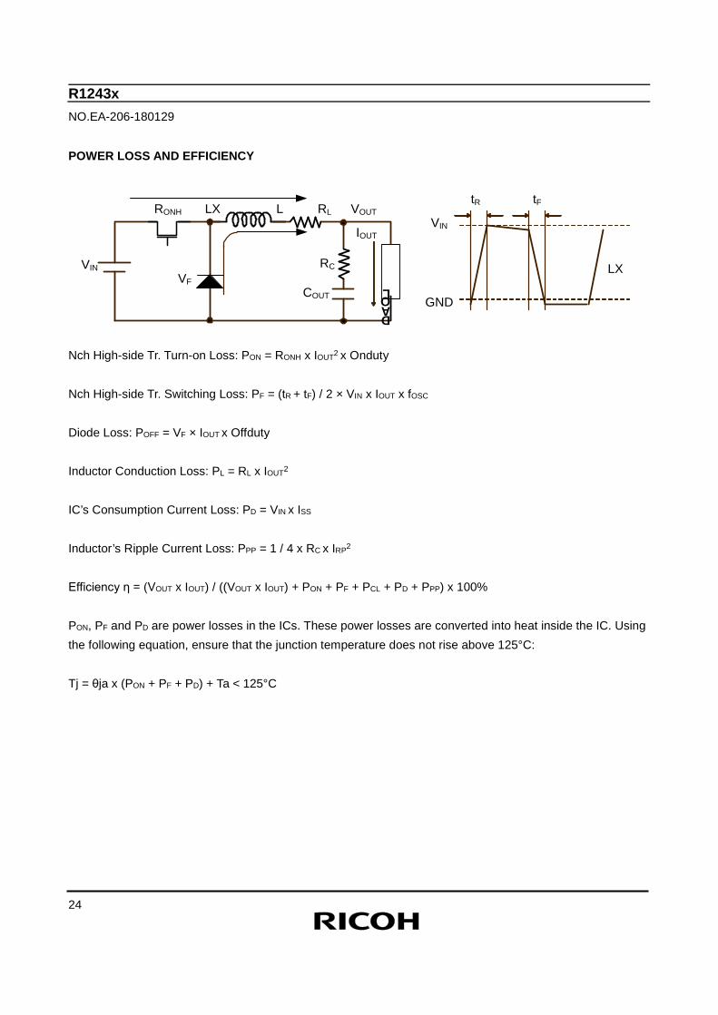
POWER LOSS AND EFFICIENCY
Nch High-side Tr. Turn-on Loss: PON = RONH x IOUT2 x Onduty Nch High-side Tr. Switching Loss: PF = (tR + tF) / 2 × VIN x IOUT x fOSC Diode Loss: POFF = VF × IOUT x Offduty Inductor Conduction Loss: PL = RL x IOUT2 IC’s Consumption Current Loss: PD = VIN x ISS Inductor’s Ripple Current Loss: PPP = 1 / 4 x RC x IRP2 Efficiency η = (VOUT x IOUT) / ((VOUT x IOUT) + PON + PF + PCL + PD + PPP) x 100% PON, PF and PD are power losses in the ICs. These power losses are converted into heat inside the IC. Using the following equation, ensure that the junction temperature does not rise above 125°C: Tj = θja x (PON + PF + PD) + Ta < 125°C
LOAD
RONH LX L
VFCOUT
RL VOUT
IOUT
RCVIN
VIN
GND
tR tF
LX
R1243x NO.EA-206-180129
25
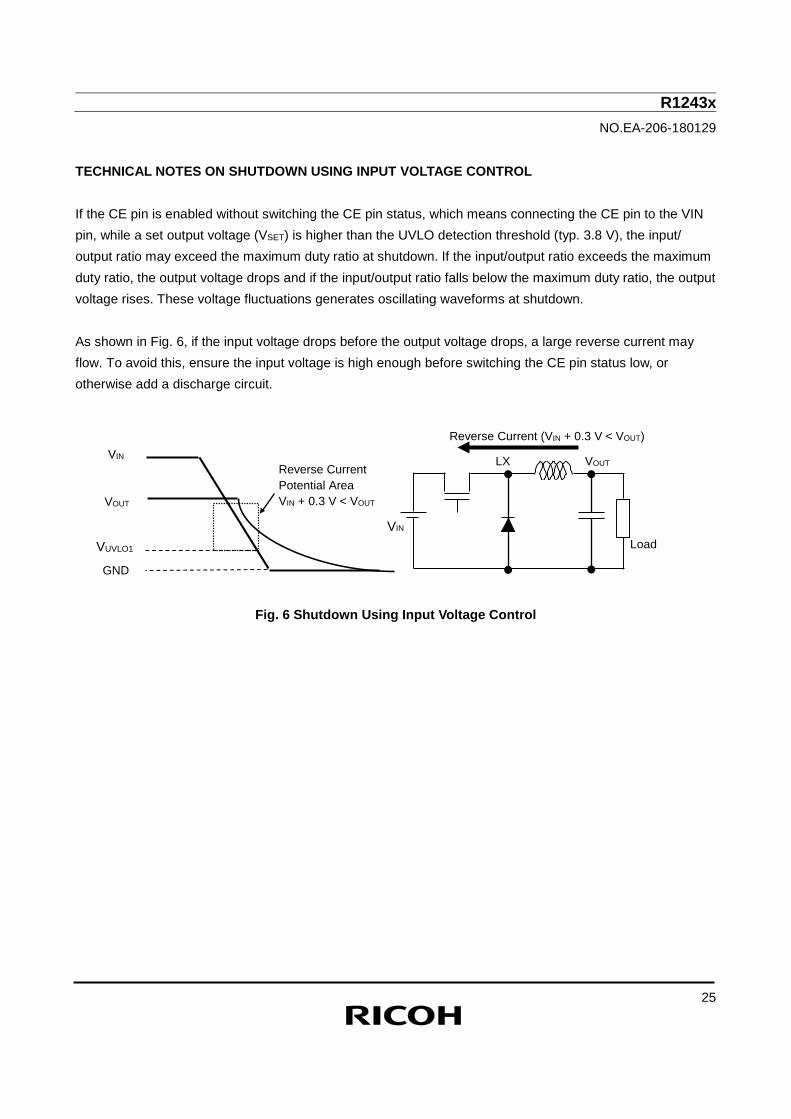
TECHNICAL NOTES ON SHUTDOWN USING INPUT VOLTAGE CONTROL If the CE pin is enabled without switching the CE pin status, which means connecting the CE pin to the VIN pin, while a set output voltage (VSET) is higher than the UVLO detection threshold (typ. 3.8 V), the input/ output ratio may exceed the maximum duty ratio at shutdown. If the input/output ratio exceeds the maximum duty ratio, the output voltage drops and if the input/output ratio falls below the maximum duty ratio, the output voltage rises. These voltage fluctuations generates oscillating waveforms at shutdown. As shown in Fig. 6, if the input voltage drops before the output voltage drops, a large reverse current may flow. To avoid this, ensure the input voltage is high enough before switching the CE pin status low, or otherwise add a discharge circuit.
Fig. 6 Shutdown Using Input Voltage Control
Load
VOUT
GND
LX VOUT
VIN
Reverse Current (VIN + 0.3 V < VOUT)
VUVLO1
VIN Reverse Current Potential Area VIN + 0.3 V < VOUT
R1243x NO.EA-206-180129
26
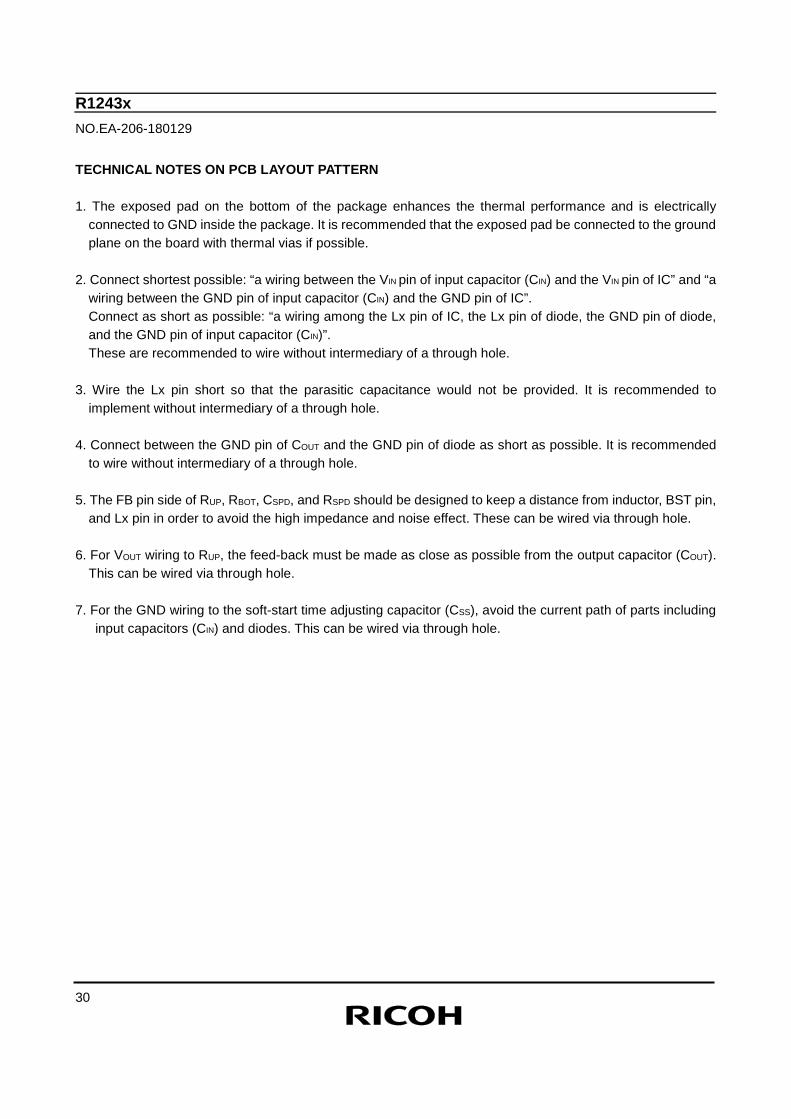
TECHNICAL NOTES
• External components have to be connected as close as possible to the IC and have to be wired as short as possible. Especially, the capacitor connected between VIN and GND pin must be wired the shortest. If the impedances of the power supply line and the GND line are high, the operation can be unstable due to the switching current, which fluctuates the power line of the inside the IC. The impedances of power supply line and GND line must be as low as possible. It is necessary to give careful consideration to the large current flowing into the power supply, GND, LX, VOUT and inductor when designing their wirings. The wiring of output voltage setting resistance (RUP) and the wiring of inductor must be separated from load wiring.
• The capacitors to be used in the R1243x must be low ESR ceramic capacitors. The CIN capacitor between VIN and GND should be equal or more than 10 µF. Please pay attention to the bias-dependent properties and the temperature variability characteristics of the ceramic capacitors.
• The internal phase compensation of this IC is designed within the recommended values of inductor and COUT ceramic capacitor. If the inductor value is small, the peak values of the switching current increase along with the load current. When the peak value of the switching current reaches to the current limit, the over current protection circuit may start to function.
• If the parasitic capacitor of the schottky diode is large, the operation may result in unstable because of the large switching current when the switch is turned on. Please use the schottky diode with 100 pF or less when the reverse voltage is 10 V.
• The output voltage (VOUT) can be calculated by this equation: VOUT = VFB × (RUP + RBOT) / RBOT. By changing RUP and RBOT, the output voltage (VOUT) is adjustable. If resistance values of RUP and RBOT are high, the impedance of the FB pins become high, and the IC becomes vulnerable to an influence of noise. RBOT is recommended to be between 1.0 kΩ to 4.7 kΩ. If the operation become unstable due to the high impedance, it is important to consider lowering the impedance.
• In the IC, ESD protection diode is connected between CE pin and VIN pin. If there is a possibility that the CE pin voltage becomes higher than the VIN pin voltage, it is recommended to insert a 10 kΩ resistance or more in order to prevent the large current flowing from CE pin into VIN pin.
• Connect the reverse side of the IC pad to GND. To improve the radiation of heat of the multiple-layered board, it is effective to make the via on the connection part of the reverse side of the IC pad to release the heat to multiple layers.
• The flag resistor (RFLG) is recommended to be between 10 kΩ to 100 kΩ. If the flag function is not used, FLG pin has to be left open or connected to GND.
• If the soft-start time adjustment function is not used, TSS pin must be left open. In this case, soft-start time is set as 0.4 ms (Typ.).
• After the completion of the soft-start, latch function (R1243x001A/C/E) starts to function. The internal counter starts counting when the overcurrent protection circuits runs the current limit detection. When the internal counter counts up to 2 ms typically (R1243x001A/C) or up to 0.08 ms (R1243x001E), latch function turns off the output. The turned off output can be reset when CE pin is changed to “L”, and also VIN pin voltage became less than 3.8 V typically, which is UVLO detecting voltage. If the output voltage becomes more than the setting voltage (FB pin voltage is 0.50 V typically within the latch timer period, the counter restores the default. Therefore, the careful attention is required when the power-supply voltage’s start-up is slow and the output voltage is not reached to the setting voltage within the latch timer period after the completion of the soft-start.
R1243x NO.EA-206-180129
27
• After the completion of the soft-start, fold-back function (R1243x001B/D) starts to function. The fold-back function limits the oscillation frequencies into 1/4 when FB pin voltage becomes less than 0.35 V (Typ.). Therefore, the careful attention is required when the power-supply voltage’s start-up is slow and the output voltage is not reached to the 70% (Typ.) of the setting voltage even for a short period of time after the completion of the soft-start.
• The quality of the power supply circuit using the R1243x largely depends on the external components. The careful attention is required for the external component parameters.
• The careful attention is required for the maximum ratings (voltage, current, and wattage) of the external components, board layout pattern and the IC.
• The table on the next page shows the recommended values for setting output voltage.
R1243x NO.EA-206-180129
28
Table 1. R1243x Recommended Value for Each Output Voltage R1243x001A/B/E: 1000 kHz
VIN VOUT L [µH] COUT [µF] CSPD CBST [µF] RBOT [kΩ] 4.5 ≤ VIN ≤ Max 0.8 ≤ VOUT ≤ 1.2 2.2 47 ∗1 0.47 2.0 4.5 ≤ VIN ≤ Max 1.2 ≤ VOUT ≤ 1.8 2.2 22 ∗1 0.47 2.0 4.5 ≤ VIN ≤ Max 1.8 ≤ VOUT ≤ 2.5 4.7 10 ∗1 0.47 2.0
4.5 ≤ VIN ≤ 6 2.5 ≤ VOUT ≤ Maxduty 4.7 22 open 0.47 2.0 6 ≤ VIN ≤ Max 2.5 ≤ VOUT ≤ 5 4.7 10 ∗1 0.47 2.0
Min ≤ VIN ≤ Max 5 ≤ VOUT ≤ Maxduty 4.7 10 ∗1 0.47 2.0
R1243x001C/D: 330 kHz
VIN VOUT L [µH] COUT [µF] CSPD CBST [µF] RBOT [kΩ] 4.5 ≤ VIN ≤ 7.5 0.8 ≤ VOUT ≤ 1.2 4.7 47×2 open 0.47 2.0 4.5 ≤ VIN ≤ 7.5 1.2 ≤ VOUT ≤ Maxduty 10 47×2 open 0.47 2.0 7.5 ≤ VIN ≤ Max 0.8 ≤ VOUT ≤ 1.2 4.7 47×2 ∗2 0.47 2.0 7.5 ≤ VIN ≤ 12 1.2 ≤ VOUT ≤ 2.5 10 47 ∗2 0.47 2.0 7.5 ≤ VIN ≤ Max 1.2 ≤ VOUT ≤ 2.5 4.7 47 ∗2 0.47 2.0 7.5 ≤ VIN ≤ Max 2.5 ≤ VOUT ≤ 5 10 22 ∗2 0.47 2.0 7.5 ≤ VIN ≤ Max 5 ≤ VOUT ≤ 18 10 10×2 ∗2 0.47 2.0
∗1 R1243x001A/B/E: 1000 kHz ∗2 R1243x001C/D: 330 kHz VOUT [V] CSPD [pF] RUP [kΩ] RBOT [kΩ] VOUT [V] CSPD [pF] RUP [kΩ] RBOT [kΩ]
0.8 1800 1.2 2.0 0.8 2700 1.2 2.0 1 1200 2.0 2.0 1 2200 2.0 2.0
1.2 1000 2.8 2.0 1.2 1500 2.8 2.0 1.5 820 4.0 2.0 1.5 1200 4.0 2.0 1.8 560 5.2 2.0 1.8 1000 5.2 2.0 2.5 390 8.0 2.0 2.5 560 8.0 2.0 3.3 220 11.2 2.0 3.3 390 11.2 2.0 5 150 18.0 2.0 5 220 18.0 2.0 6 120 22.0 2.0 6 180 22.0 2.0 9 82 34.0 2.0 9 150 34.0 2.0
12 56 46.0 2.0 12 100 46.0 2.0 15 47 58.0 2.0 15 100 58.0 2.0 18 47 70.0 2.0 18 100 70.0 2.0
R1243x NO.EA-206-180129
29
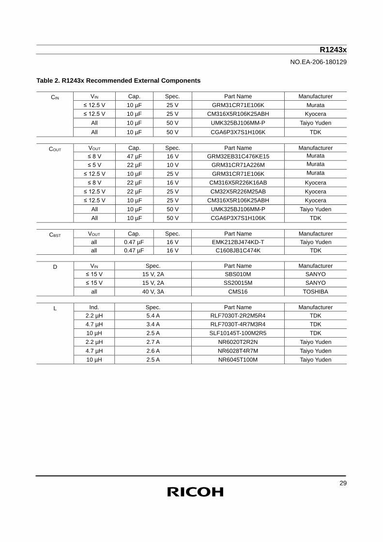
Table 2. R1243x Recommended External Components
CIN VIN Cap. Spec. Part Name Manufacturer ≤ 12.5 V 10 µF 25 V GRM31CR71E106K Murata ≤ 12.5 V 10 µF 25 V CM316X5R106K25ABH Kyocera
All 10 µF 50 V UMK325BJ106MM-P Taiyo Yuden All 10 µF 50 V CGA6P3X7S1H106K TDK
COUT VOUT Cap. Spec. Part Name Manufacturer
≤ 8 V 47 µF 16 V GRM32EB31C476KE15 Murata ≤ 5 V 22 µF 10 V GRM31CR71A226M Murata
≤ 12.5 V 10 µF 25 V GRM31CR71E106K Murata ≤ 8 V 22 µF 16 V CM316X5R226K16AB Kyocera
≤ 12.5 V 22 µF 25 V CM32X5R226M25AB Kyocera ≤ 12.5 V 10 µF 25 V CM316X5R106K25ABH Kyocera
All 10 µF 50 V UMK325BJ106MM-P Taiyo Yuden All 10 µF 50 V CGA6P3X7S1H106K TDK
CBST VOUT Cap. Spec. Part Name Manufacturer
all 0.47 µF 16 V EMK212BJ474KD-T Taiyo Yuden all 0.47 µF 16 V C1608JB1C474K TDK
D VIN Spec. Part Name Manufacturer
≤ 15 V 15 V, 2A SBS010M SANYO ≤ 15 V 15 V, 2A SS20015M SANYO
all 40 V, 3A CMS16 TOSHIBA
L Ind. Spec. Part Name Manufacturer 2.2 µH 5.4 A RLF7030T-2R2M5R4 TDK 4.7 µH 3.4 A RLF7030T-4R7M3R4 TDK 10 µH 2.5 A SLF10145T-100M2R5 TDK 2.2 µH 2.7 A NR6020T2R2N Taiyo Yuden 4.7 µH 2.6 A NR6028T4R7M Taiyo Yuden 10 µH 2.5 A NR6045T100M Taiyo Yuden
R1243x NO.EA-206-180129
30
TECHNICAL NOTES ON PCB LAYOUT PATTERN 1. The exposed pad on the bottom of the package enhances the thermal performance and is electrically
connected to GND inside the package. It is recommended that the exposed pad be connected to the ground plane on the board with thermal vias if possible.
2. Connect shortest possible: “a wiring between the VIN pin of input capacitor (CIN) and the VIN pin of IC” and “a
wiring between the GND pin of input capacitor (CIN) and the GND pin of IC”. Connect as short as possible: “a wiring among the Lx pin of IC, the Lx pin of diode, the GND pin of diode, and the GND pin of input capacitor (CIN)”. These are recommended to wire without intermediary of a through hole.
3. Wire the Lx pin short so that the parasitic capacitance would not be provided. It is recommended to
implement without intermediary of a through hole. 4. Connect between the GND pin of COUT and the GND pin of diode as short as possible. It is recommended
to wire without intermediary of a through hole. 5. The FB pin side of RUP, RBOT, CSPD, and RSPD should be designed to keep a distance from inductor, BST pin,
and Lx pin in order to avoid the high impedance and noise effect. These can be wired via through hole. 6. For VOUT wiring to RUP, the feed-back must be made as close as possible from the output capacitor (COUT).
This can be wired via through hole. 7. For the GND wiring to the soft-start time adjusting capacitor (CSS), avoid the current path of parts including
input capacitors (CIN) and diodes. This can be wired via through hole.
R1243x NO.EA-206-180129
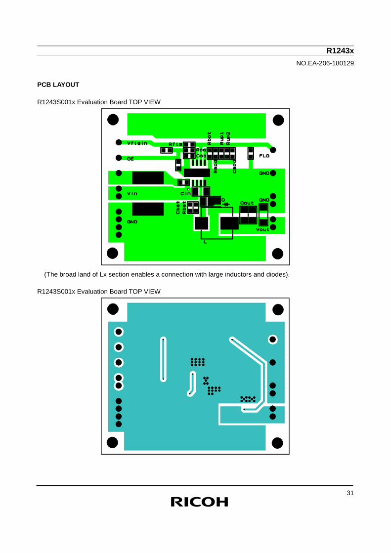
31
PCB LAYOUT R1243S001x Evaluation Board TOP VIEW
(The broad land of Lx section enables a connection with large inductors and diodes).
R1243S001x Evaluation Board TOP VIEW
R1243x NO.EA-206-180129
32
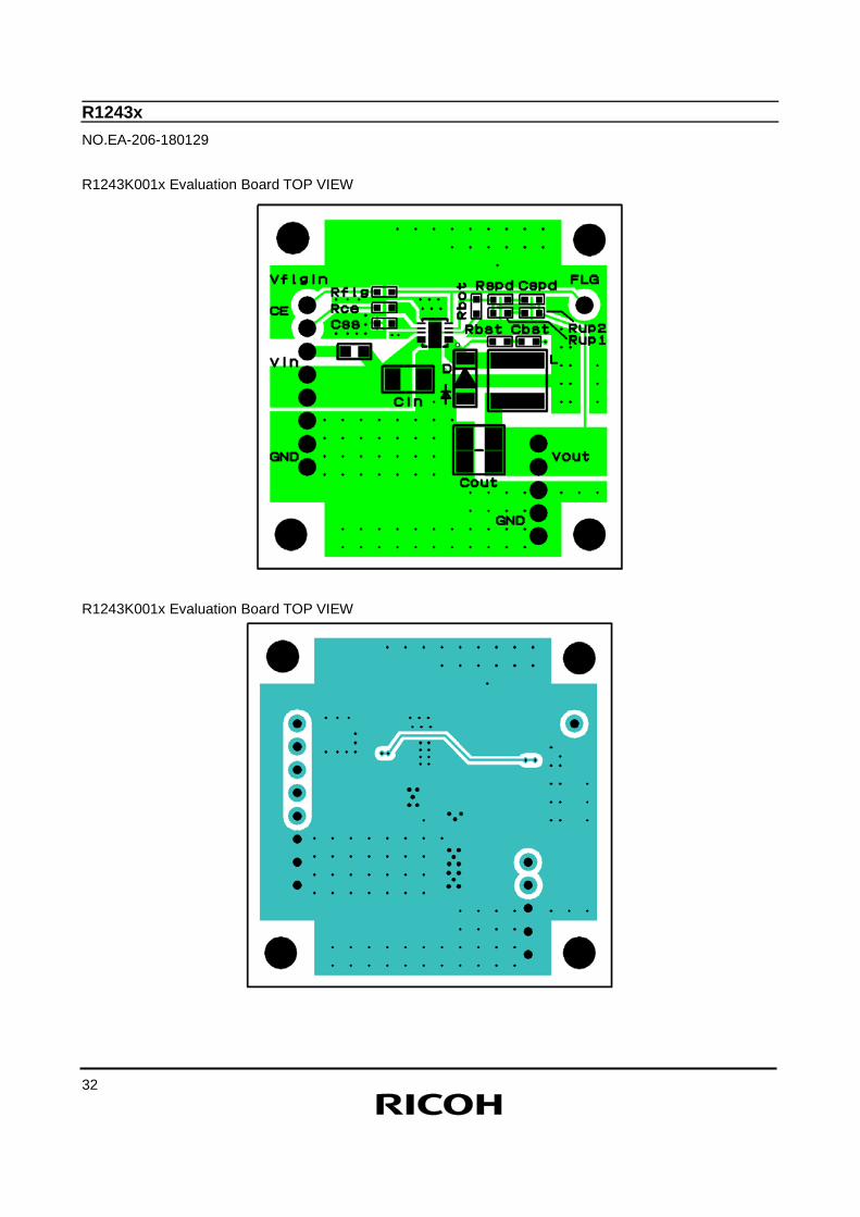
R1243K001x Evaluation Board TOP VIEW
R1243K001x Evaluation Board TOP VIEW
R1243x NO.EA-206-180129
33
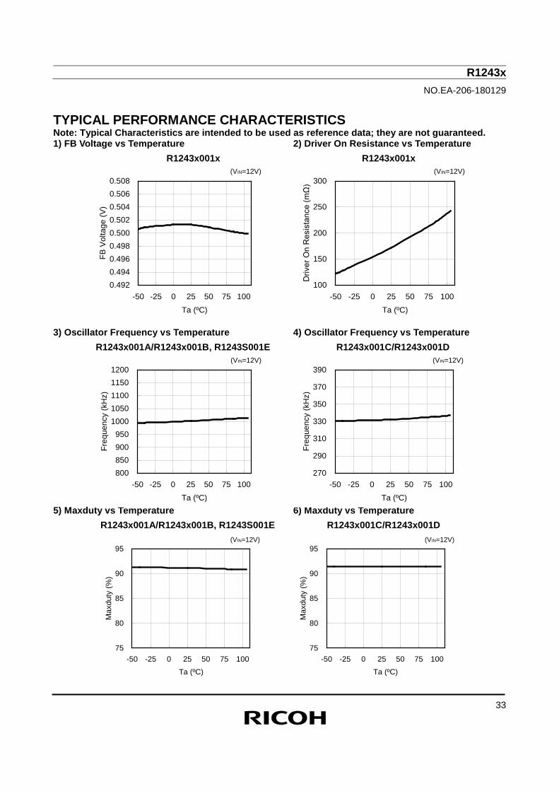
TYPICAL PERFORMANCE CHARACTERISTICS Note: Typical Characteristics are intended to be used as reference data; they are not guaranteed. 1) FB Voltage vs Temperature 2) Driver On Resistance vs Temperature R1243x001x R1243x001x 3) Oscillator Frequency vs Temperature 4) Oscillator Frequency vs Temperature
R1243x001A/R1243x001B, R1243S001E R1243x001C/R1243x001D 5) Maxduty vs Temperature 6) Maxduty vs Temperature R1243x001A/R1243x001B, R1243S001E R1243x001C/R1243x001D
(VIN=12V) (VIN=12V)
0.4920.4940.4960.4980.5000.5020.5040.5060.508
-50 -25 0 25 50 75 100
Ta (ºC)
FB V
olta
ge (V
)
100
150
200
250
300
-50 -25 0 25 50 75 100
Ta (ºC)D
river
On
Res
ista
nce
(mΩ
)
(VIN=12V) (VIN=12V)
800850900950
10001050110011501200
-50 -25 0 25 50 75 100
Ta (ºC)
Freq
uenc
y (k
Hz)
270
290
310
330
350
370
390
-50 -25 0 25 50 75 100
Ta (ºC)
Freq
uenc
y (k
Hz)
(VIN=12V) (VIN=12V)
75
80
85
90
95
-50 -25 0 25 50 75 100
Ta (ºC)
Max
duty
(%)
75
80
85
90
95
-50 -25 0 25 50 75 100
Ta (ºC)
Max
duty
(%)
R1243x NO.EA-206-180129
34
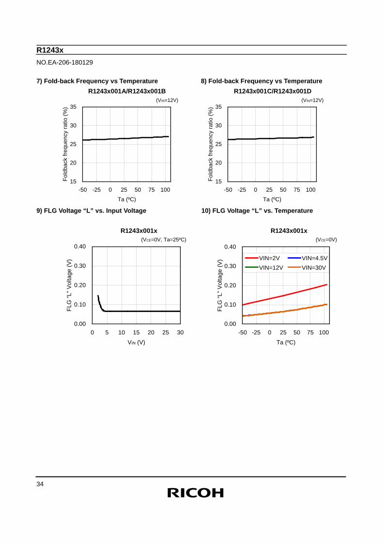
7) Fold-back Frequency vs Temperature 8) Fold-back Frequency vs Temperature R1243x001A/R1243x001B R1243x001C/R1243x001D 9) FLG Voltage “L” vs. Input Voltage 10) FLG Voltage “L” vs. Temperature
R1243x001x R1243x001x
(VCE=0V, Ta=25ºC) (VCE=0V)
0.00
0.10
0.20
0.30
0.40
0 5 10 15 20 25 30
VIN (V)
FLG
“L” V
olta
ge (V
)
0.00
0.10
0.20
0.30
0.40
-50 -25 0 25 50 75 100
Ta (ºC)
FLG
“L” V
olta
ge (V
) VIN=2V VIN=4.5VVIN=12V VIN=30V
(VIN=12V) (VIN=12V)
15
20
25
30
35
-50 -25 0 25 50 75 100
Ta (ºC)
Fold
back
freq
uenc
y ra
tio (%
)
15
20
25
30
35
-50 -25 0 25 50 75 100
Ta (ºC)
Fold
back
freq
uenc
y ra
tio (%
)
R1243x NO.EA-206-180129
35
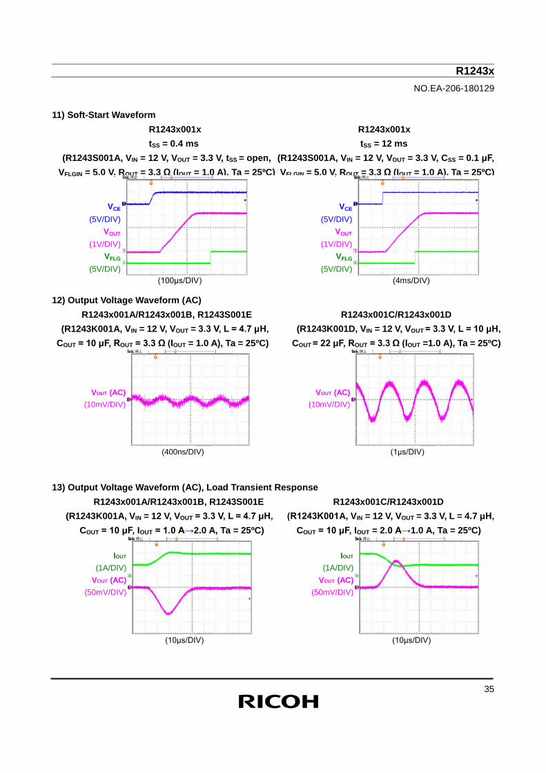
11) Soft-Start Waveform R1243x001x R1243x001x tSS = 0.4 ms tSS = 12 ms (R1243S001A, VIN = 12 V, VOUT = 3.3 V, tSS = open, (R1243S001A, VIN = 12 V, VOUT = 3.3 V, CSS = 0.1 μF, VFLGIN = 5.0 V, ROUT = 3.3 Ω (IOUT = 1.0 A), Ta = 25ºC) VFLGIN = 5.0 V, ROUT = 3.3 Ω (IOUT = 1.0 A), Ta = 25ºC) 12) Output Voltage Waveform (AC) R1243x001A/R1243x001B, R1243S001E R1243x001C/R1243x001D
(R1243K001A, VIN = 12 V, VOUT = 3.3 V, L = 4.7 μH, (R1243K001D, VIN = 12 V, VOUT = 3.3 V, L = 10 μH, COUT = 10 μF, ROUT = 3.3 Ω (IOUT = 1.0 A), Ta = 25ºC) COUT = 22 μF, ROUT = 3.3 Ω (IOUT =1.0 A), Ta = 25ºC)
13) Output Voltage Waveform (AC), Load Transient Response
R1243x001A/R1243x001B, R1243S001E R1243x001C/R1243x001D (R1243K001A, VIN = 12 V, VOUT = 3.3 V, L = 4.7 μH, (R1243K001A, VIN = 12 V, VOUT = 3.3 V, L = 4.7 μH,
COUT = 10 μF, IOUT = 1.0 A→2.0 A, Ta = 25ºC) COUT = 10 μF, IOUT = 2.0 A→1.0 A, Ta = 25ºC)
VOUT (AC) VOUT (AC)(10mV/DIV) (10mV/DIV)
(400ns/DIV) (1μs/DIV)
IOUT IOUT
(1A/DIV) (1A/DIV)VOUT (AC) VOUT (AC)
(50mV/DIV) (50mV/DIV)
(10μs/DIV) (10μs/DIV)
VCE VCE
(5V/DIV) (5V/DIV)VOUT VOUT
(1V/DIV) (1V/DIV)VFLG VFLG
(5V/DIV) (5V/DIV)(100μs/DIV) (4ms/DIV)
R1243x NO.EA-206-180129
36
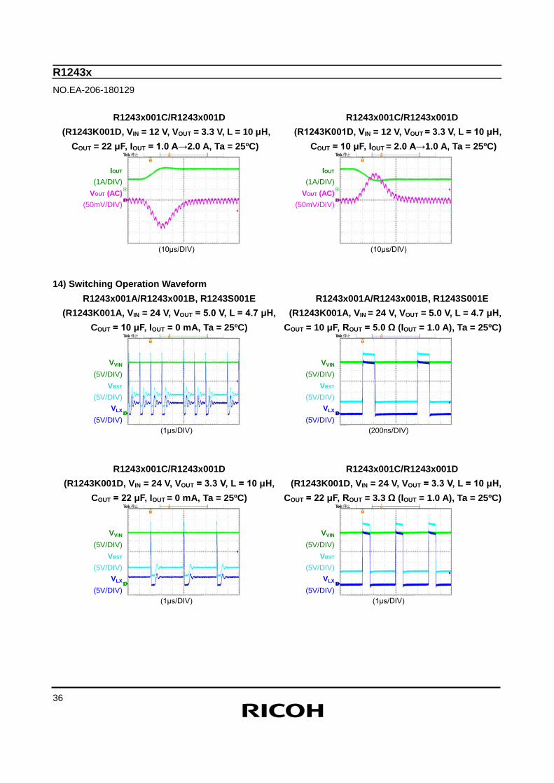
R1243x001C/R1243x001D R1243x001C/R1243x001D (R1243K001D, VIN = 12 V, VOUT = 3.3 V, L = 10 μH, (R1243K001D, VIN = 12 V, VOUT = 3.3 V, L = 10 μH,
COUT = 22 μF, IOUT = 1.0 A→2.0 A, Ta = 25ºC) COUT = 10 μF, IOUT = 2.0 A→1.0 A, Ta = 25ºC)
14) Switching Operation Waveform R1243x001A/R1243x001B, R1243S001E R1243x001A/R1243x001B, R1243S001E (R1243K001A, VIN = 24 V, VOUT = 5.0 V, L = 4.7 μH, (R1243K001A, VIN = 24 V, VOUT = 5.0 V, L = 4.7 μH, COUT = 10 μF, IOUT = 0 mA, Ta = 25ºC) COUT = 10 μF, ROUT = 5.0 Ω (IOUT = 1.0 A), Ta = 25ºC)
R1243x001C/R1243x001D R1243x001C/R1243x001D (R1243K001D, VIN = 24 V, VOUT = 3.3 V, L = 10 μH, (R1243K001D, VIN = 24 V, VOUT = 3.3 V, L = 10 μH, COUT = 22 μF, IOUT = 0 mA, Ta = 25ºC) COUT = 22 μF, ROUT = 3.3 Ω (IOUT = 1.0 A), Ta = 25ºC)
IOUT IOUT
(1A/DIV) (1A/DIV)VOUT (AC) VOUT (AC)
(50mV/DIV) (50mV/DIV)
(10μs/DIV) (10μs/DIV)
VVIN VVIN
(5V/DIV) (5V/DIV)VBST VBST
(5V/DIV) (5V/DIV)VLX VLX
(5V/DIV) (5V/DIV)(1μs/DIV) (200ns/DIV)
VVIN VVIN
(5V/DIV) (5V/DIV)VBST VBST
(5V/DIV) (5V/DIV)VLX VLX
(5V/DIV) (5V/DIV)(1μs/DIV) (1μs/DIV)
R1243x NO.EA-206-180129
37
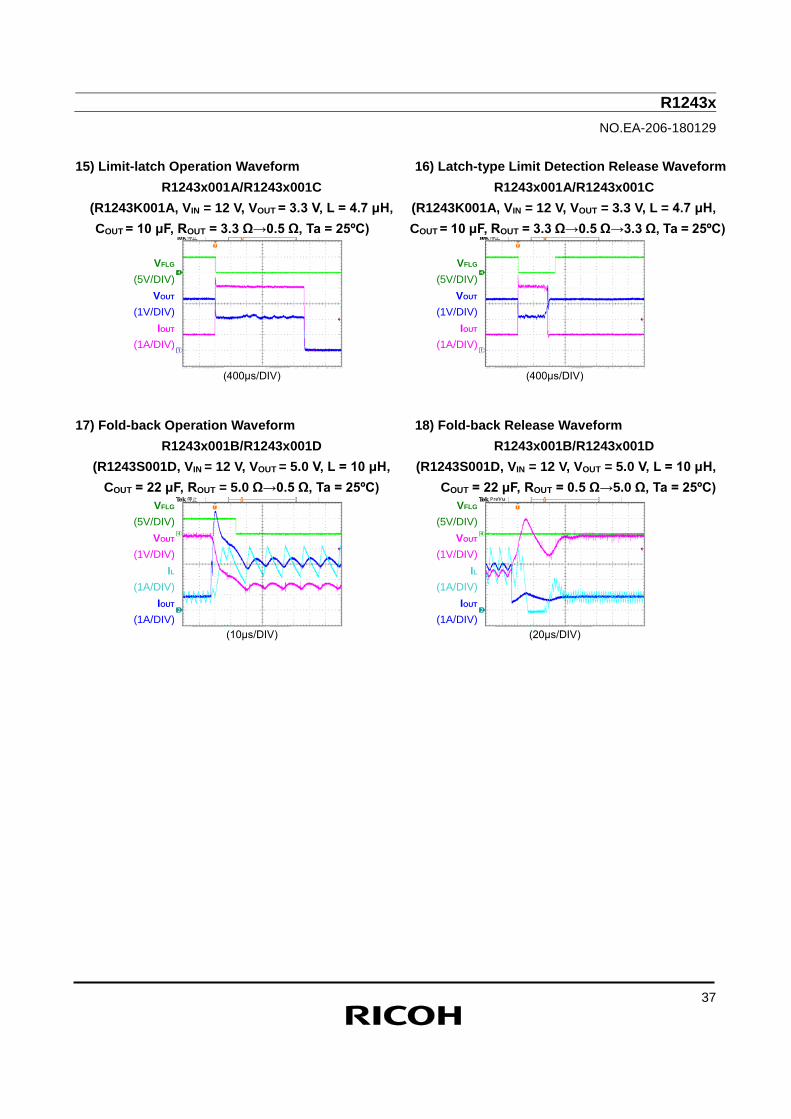
15) Limit-latch Operation Waveform 16) Latch-type Limit Detection Release Waveform R1243x001A/R1243x001C R1243x001A/R1243x001C (R1243K001A, VIN = 12 V, VOUT = 3.3 V, L = 4.7 μH, (R1243K001A, VIN = 12 V, VOUT = 3.3 V, L = 4.7 μH,
COUT = 10 μF, ROUT = 3.3 Ω→0.5 Ω, Ta = 25ºC) COUT = 10 μF, ROUT = 3.3 Ω→0.5 Ω→3.3 Ω, Ta = 25ºC)
17) Fold-back Operation Waveform 18) Fold-back Release Waveform R1243x001B/R1243x001D R1243x001B/R1243x001D (R1243S001D, VIN = 12 V, VOUT = 5.0 V, L = 10 μH, (R1243S001D, VIN = 12 V, VOUT = 5.0 V, L = 10 μH, COUT = 22 μF, ROUT = 5.0 Ω→0.5 Ω, Ta = 25ºC) COUT = 22 μF, ROUT = 0.5 Ω→5.0 Ω, Ta = 25ºC)
VFLG VFLG
(5V/DIV) (5V/DIV)VOUT VOUT
(1V/DIV) (1V/DIV)IOUT IOUT
(1A/DIV) (1A/DIV)
(400μs/DIV) (400μs/DIV)
VFLG VFLG
(5V/DIV) (5V/DIV)VOUT VOUT
(1V/DIV) (1V/DIV)IL IL
(1A/DIV) (1A/DIV)IOUT IOUT
(1A/DIV) (1A/DIV)(10μs/DIV) (20μs/DIV)
R1243x NO.EA-206-180129
38
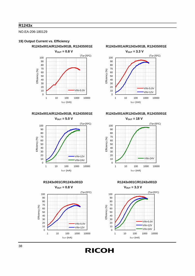
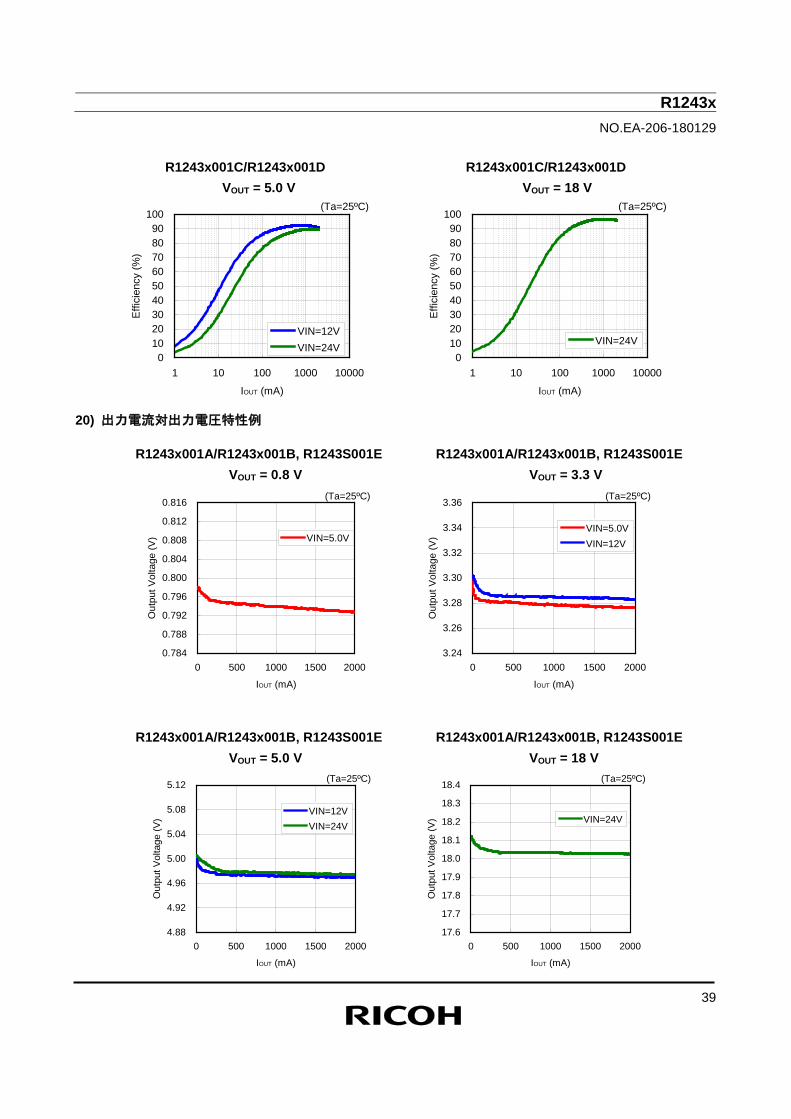
19) Output Current vs. Efficiency R1243x001A/R1243x001B, R1243S001E R1243x001A/R1243x001B, R1243S001E
VOUT = 0.8 V VOUT = 3.3 V
R1243x001A/R1243x001B, R1243S001E R1243x001A/R1243x001B, R1243S001E VOUT = 5.0 V VOUT = 18 V
R1243x001C/R1243x001D R1243x001C/R1243x001D VOUT = 0.8 V VOUT = 3.3 V
(Ta=25ºC) (Ta=25ºC)
0102030405060708090
100
1 10 100 1000 10000
IOUT (mA)
Effi
cien
cy (%
)
VIN=5.0V0
102030405060708090
100
1 10 100 1000 10000
IOUT (mA)E
ffici
ency
(%)
VIN=5.0VVIN=12V
(Ta=25ºC) (Ta=25ºC)
0102030405060708090
100
1 10 100 1000 10000
IOUT (mA)
Effi
cien
cy (%
)
VIN=12VVIN=24V
0102030405060708090
100
1 10 100 1000 10000
IOUT (mA)
Effi
cien
cy (%
)
VIN=24V
(Ta=25ºC) (Ta=25ºC)
0102030405060708090
100
1 10 100 1000 10000
IOUT (mA)
Effi
cien
cy (%
)
VIN=5.0VVIN=12V
0102030405060708090
100
1 10 100 1000 10000
IOUT (mA)
Effi
cien
cy (%
)
VIN=5.0VVIN=12VVIN=24V
R1243x NO.EA-206-180129
39
R1243x001C/R1243x001D R1243x001C/R1243x001D VOUT = 5.0 V VOUT = 18 V
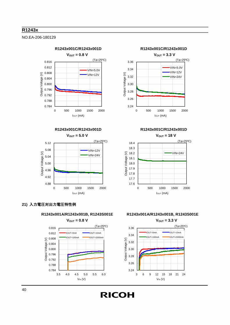
20) 出力電流対出力電圧特性例
R1243x001A/R1243x001B, R1243S001E R1243x001A/R1243x001B, R1243S001E VOUT = 0.8 V VOUT = 3.3 V
R1243x001A/R1243x001B, R1243S001E R1243x001A/R1243x001B, R1243S001E VOUT = 5.0 V VOUT = 18 V
(Ta=25ºC) (Ta=25ºC)
0102030405060708090
100
1 10 100 1000 10000
IOUT (mA)
Effi
cien
cy (%
)
VIN=24V0
102030405060708090
100
1 10 100 1000 10000
IOUT (mA)
Effi
cien
cy (%
)
VIN=12VVIN=24V
(Ta=25ºC) (Ta=25ºC)
0.784
0.788
0.792
0.796
0.800
0.804
0.808
0.812
0.816
0 500 1000 1500 2000
IOUT (mA)
Out
put V
olta
ge (V
) VIN=5.0V
3.24
3.26
3.28
3.30
3.32
3.34
3.36
0 500 1000 1500 2000
IOUT (mA)
Out
put V
olta
ge (V
)
VIN=5.0VVIN=12V
(Ta=25ºC) (Ta=25ºC)
4.88
4.92
4.96
5.00
5.04
5.08
5.12
0 500 1000 1500 2000
IOUT (mA)
Out
put V
olta
ge (V
)
VIN=12VVIN=24V
17.6
17.7
17.8
17.9
18.0
18.1
18.2
18.3
18.4
0 500 1000 1500 2000
IOUT (mA)
Out
put V
olta
ge (V
) VIN=24V
R1243x NO.EA-206-180129
40
R1243x001C/R1243x001D R1243x001C/R1243x001D VOUT = 0.8 V VOUT = 3.3 V
R1243x001C/R1243x001D R1243x001C/R1243x001D VOUT = 5.0 V VOUT = 18 V
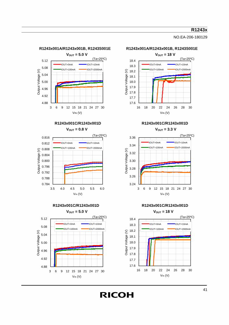
21) 入力電圧対出力電圧特性例
R1243x001A/R1243x001B, R1243S001E R1243x001A/R1243x001B, R1243S001E VOUT = 0.8 V VOUT = 3.3 V
(Ta=25ºC) (Ta=25ºC)
0.784
0.788
0.792
0.796
0.800
0.804
0.808
0.812
0.816
0 500 1000 1500 2000
IOUT (mA)
Out
put V
olta
ge (V
) VIN=5.0VVIN=12V
3.24
3.26
3.28
3.30
3.32
3.34
3.36
0 500 1000 1500 2000
IOUT (mA)
Out
put V
olta
ge (V
)
VIN=5.0VVIN=12VVIN=24V
(Ta=25ºC) (Ta=25ºC)
17.6
17.7
17.8
17.9
18.0
18.1
18.2
18.3
18.4
0 500 1000 1500 2000
IOUT (mA)
Out
put V
olta
ge (V
) VIN=24V
4.88
4.92
4.96
5.00
5.04
5.08
5.12
0 500 1000 1500 2000
IOUT (mA)
Out
put V
olta
ge (V
) VIN=12VVIN=24V
(Ta=25ºC) (Ta=25ºC)
0.784
0.788
0.792
0.796
0.800
0.804
0.808
0.812
0.816
3.5 4.0 4.5 5.0 5.5 6.0
VIN (V)
Out
put V
olta
ge (V
)
IOUT=0mA IOUT=10mA
IOUT=100mA IOUT=2000mA
3.24
3.26
3.28
3.30
3.32
3.34
3.36
3 6 9 12 15 18 21 24
VIN (V)
Out
put V
olta
ge (V
)
IOUT=0mA IOUT=10mA
IOUT=100mA IOUT=2000mA
R1243x NO.EA-206-180129
41
R1243x001A/R1243x001B, R1243S001E R1243x001A/R1243x001B, R1243S001E VOUT = 5.0 V VOUT = 18 V
R1243x001C/R1243x001D R1243x001C/R1243x001D VOUT = 0.8 V VOUT = 3.3 V
R1243x001C/R1243x001D R1243x001C/R1243x001D VOUT = 5.0 V VOUT = 18 V
(Ta=25ºC) (Ta=25ºC)
0.784
0.788
0.792
0.796
0.800
0.804
0.808
0.812
0.816
3.5 4.0 4.5 5.0 5.5 6.0
VIN (V)
Out
put V
olta
ge (V
)
IOUT=0mA IOUT=10mA
IOUT=100mA IOUT=2000mA
3.24
3.26
3.28
3.30
3.32
3.34
3.36
3 6 9 12 15 18 21 24 27 30
VIN (V)
Out
put V
olta
ge (V
)
IOUT=0mA IOUT=10mA
IOUT=100mA IOUT=2000mA
(Ta=25ºC) (Ta=25ºC)
4.88
4.92
4.96
5.00
5.04
5.08
5.12
3 6 9 12 15 18 21 24 27 30
VIN (V)
Out
put V
olta
ge (V
)
IOUT=0mA IOUT=10mA
IOUT=100mA IOUT=2000mA
17.6
17.7
17.8
17.9
18.0
18.1
18.2
18.3
18.4
16 18 20 22 24 26 28 30
VIN (V)
Out
put V
olta
ge (V
)
IOUT=0mA IOUT=10mA
IOUT=100mA IOUT=2000mA
(Ta=25ºC) (Ta=25ºC)
4.88
4.92
4.96
5.00
5.04
5.08
5.12
3 6 9 12 15 18 21 24 27 30
VIN (V)
Out
put V
olta
ge (V
)
IOUT=0mA IOUT=10mA
IOUT=100mA IOUT=2000mA
17.6
17.7
17.8
17.9
18.0
18.1
18.2
18.3
18.4
16 18 20 22 24 26 28 30
VIN (V)
Out
put V
olta
ge (V
)
IOUT=0mA IOUT=10mA
IOUT=100mA IOUT=2000mA
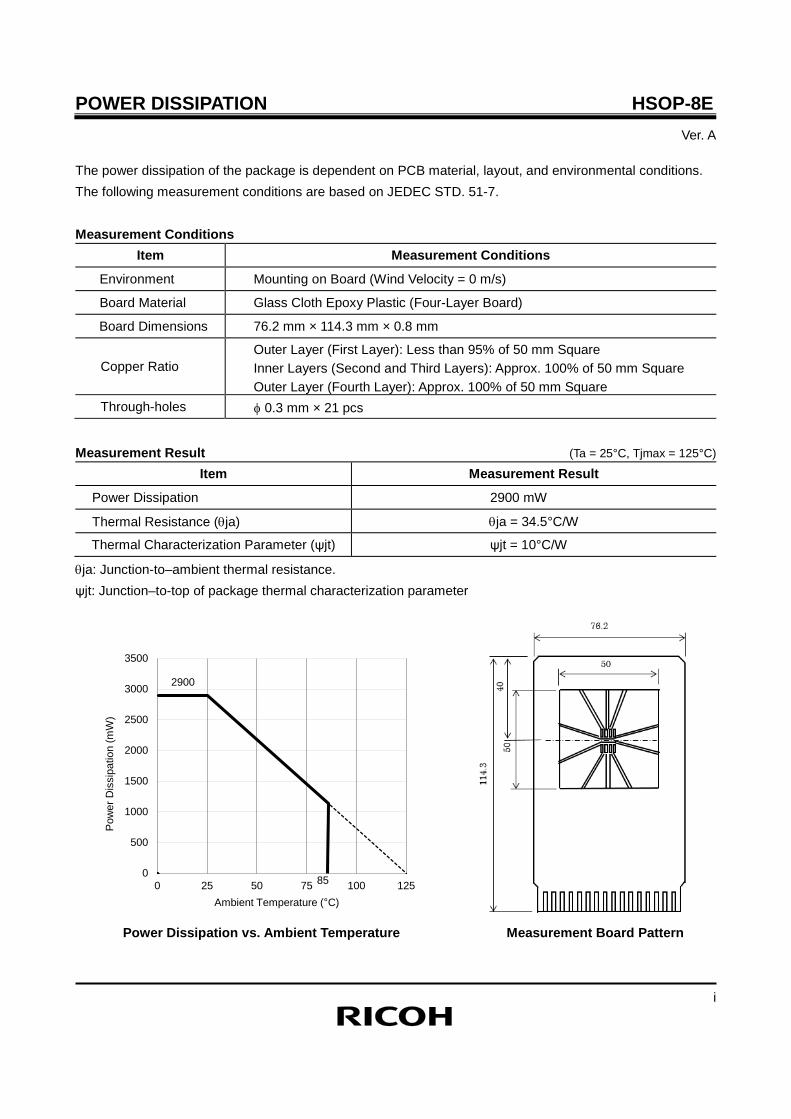
POWER DISSIPATION HSOP-8E
Ver. A
i
The power dissipation of the package is dependent on PCB material, layout, and environmental conditions. The following measurement conditions are based on JEDEC STD. 51-7. Measurement Conditions
Item Measurement Conditions
Environment Mounting on Board (Wind Velocity = 0 m/s)
Board Material Glass Cloth Epoxy Plastic (Four-Layer Board)
Board Dimensions 76.2 mm × 114.3 mm × 0.8 mm
Copper Ratio Outer Layer (First Layer): Less than 95% of 50 mm Square Inner Layers (Second and Third Layers): Approx. 100% of 50 mm Square Outer Layer (Fourth Layer): Approx. 100% of 50 mm Square
Through-holes φ 0.3 mm × 21 pcs
Measurement Result (Ta = 25°C, Tjmax = 125°C)
Item Measurement Result
Power Dissipation 2900 mW
Thermal Resistance (θja) θja = 34.5°C/W
Thermal Characterization Parameter (ψjt) ψjt = 10°C/W
θja: Junction-to–ambient thermal resistance. ψjt: Junction–to-top of package thermal characterization parameter
Power Dissipation vs. Ambient Temperature Measurement Board Pattern
0
500
1000
1500
2000
2500
3000
3500
0 25 50 75 100 125
Pow
er D
issi
patio
n (m
W)
Ambient Temperature (°C)
2900
85
PACKAGE DIMENSIONS HSOP-8E
i
HSOP-8E Package Dimensions
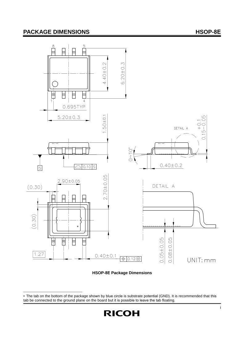
∗ The tab on the bottom of the package shown by blue circle is substrate potential (GND). It is recommended that this tab be connected to the ground plane on the board but it is possible to leave the tab floating.
∗
masutani
楕円
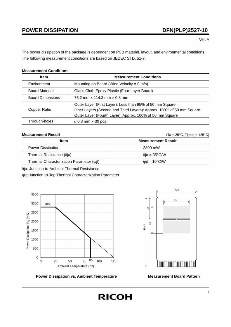
POWER DISSIPATION DFN(PLP)2527-10 Ver. A
i
The power dissipation of the package is dependent on PCB material, layout, and environmental conditions. The following measurement conditions are based on JEDEC STD. 51-7. Measurement Conditions
Item Measurement Conditions
Environment Mounting on Board (Wind Velocity = 0 m/s)
Board Material Glass Cloth Epoxy Plastic (Four-Layer Board)
Board Dimensions 76.2 mm × 114.3 mm × 0.8 mm
Copper Ratio Outer Layer (First Layer): Less than 95% of 50 mm Square Inner Layers (Second and Third Layers): Approx. 100% of 50 mm Square Outer Layer (Fourth Layer): Approx. 100% of 50 mm Square
Through-holes φ 0.3 mm × 30 pcs
Measurement Result (Ta = 25°C, Tjmax = 125°C)
Item Measurement Result
Power Dissipation 2800 mW
Thermal Resistance (θja) θja = 35°C/W
Thermal Characterization Parameter (ψjt) ψjt = 10°C/W
θja: Junction-to-Ambient Thermal Resistance ψjt: Junction-to-Top Thermal Characterization Parameter
Power Dissipation vs. Ambient Temperature Measurement Board Pattern
0
500
1000
1500
2000
2500
3000
3500
0 25 50 75 100 125
Pow
er D
issi
patio
n P D
(mW
)
Ambient Temperature (°C)
2800
85
PACKAGE DIMENSIONS DFN(PLP)2527-10Ver. A
i
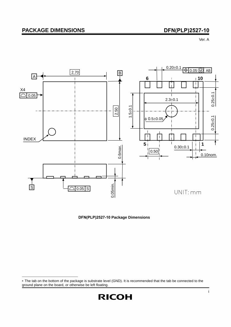
DFN(PLP)2527-10 Package Dimensions
∗ The tab on the bottom of the package is substrate level (GND). It is recommended that the tab be connected to the ground plane on the board, or otherwise be left floating.
2.50
2.70 A
B
0.05 X4
INDEX
0.6m
ax.
0.05
min
.
S 0.05 S
6 10
5 1
0.25
±0.1
0.
25±0
.1
0.10nom.
0.30±0.1
1.5±
0.1
0.50
0.20±0.1 0.05 M AB
2.3±0.1
φ 0.5±0.05
masutani
楕円
Ricoh is committed to reducing the environmental loading materials in electrical deviceswith a view to contributing to the protection of human health and the environment. Ricoh has been providing RoHS compliant products since April 1, 2006 and Halogen-free products since April 1, 2012.Halogen Free
https://www.e-devices.ricoh.co.jp/en/
Sales & Support OfficesRicoh Electronic Devices Co., Ltd.Shin-Yokohama Office (International Sales)2-3, Shin-Yokohama 3-chome, Kohoku-ku, Yokohama-shi, Kanagawa, 222-8530, JapanPhone: +81-50-3814-7687 Fax: +81-45-474-0074
Ricoh Americas Holdings, Inc.675 Campbell Technology Parkway, Suite 200 Campbell, CA 95008, U.S.A.Phone: +1-408-610-3105
Ricoh Europe (Netherlands) B.V.Semiconductor Support CentreProf. W.H. Keesomlaan 1, 1183 DJ Amstelveen, The Netherlands Phone: +31-20-5474-309
Ricoh International B.V. - German BranchSemiconductor Sales and Support CentreOberrather Strasse 6, 40472 Düsseldorf, GermanyPhone: +49-211-6546-0
Ricoh Electronic Devices Korea Co., Ltd.3F, Haesung Bldg, 504, Teheran-ro, Gangnam-gu, Seoul, 135-725, KoreaPhone: +82-2-2135-5700 Fax: +82-2-2051-5713
Ricoh Electronic Devices Shanghai Co., Ltd.Room 403, No.2 Building, No.690 Bibo Road, Pu Dong New District, Shanghai 201203, People's Republic of ChinaPhone: +86-21-5027-3200 Fax: +86-21-5027-3299
Ricoh Electronic Devices Shanghai Co., Ltd.Shenzhen Branch1205, Block D(Jinlong Building), Kingkey 100, Hongbao Road, Luohu District, Shenzhen, China Phone: +86-755-8348-7600 Ext 225
Ricoh Electronic Devices Co., Ltd.Taipei officeRoom 109, 10F-1, No.51, Hengyang Rd., Taipei City, Taiwan (R.O.C.)Phone: +886-2-2313-1621/1622 Fax: +886-2-2313-1623
1. The products and the product specifications described in this document are subject to change or discontinuation of production without notice for reasons such as improvement. Therefore, before deciding to use the products, please refer to Ricoh sales representatives for the latest information thereon.
2. The materials in this document may not be copied or otherwise reproduced in whole or in part without prior written consent of Ricoh.
3. Please be sure to take any necessary formalities under relevant laws or regulations before exporting or otherwise taking out of your country the products or the technical information described herein.
4. The technical information described in this document shows typical characteristics of and example application circuits for the products. The release of such information is not to be construed as a warranty of or a grant of license under Ricoh's or any third party's intellectual property rights or any other rights.
5. The products listed in this document are intended and designed for use as general electronic components in standard applications (office equipment, telecommunication equipment, measuring instruments, consumer electronic products, amusement equipment etc.). Those customers intending to use a product in an application requiring extreme quality and reliability, for example, in a highly specific application where the failure or misoperation of the product could result in human injury or death (aircraft, spacevehicle, nuclear reactor control system, traffic control system, automotive and transportation equipment, combustion equipment, safety devices, life support system etc.) should first contact us.
6. We are making our continuous effort to improve the quality and reliability of our products, but semiconductor products are likely to fail with certain probability. In order to prevent any injury to persons or damages to property resulting from such failure, customers should be careful enough to incorporate safety measures in their design, such as redundancy feature, fire containment feature and fail-safe feature. We do not assume any liability or responsibility for any loss or damage arising from misuse or inappropriate use of the products.
7. Anti-radiation design is not implemented in the products described in this document. 8. The X-ray exposure can influence functions and characteristics of the products. Confirm the product functions and
characteristics in the evaluation stage. 9. WLCSP products should be used in light shielded environments. The light exposure can influence functions and
characteristics of the products under operation or storage. 10. There can be variation in the marking when different AOI (Automated Optical Inspection) equipment is used. In the
case of recognizing the marking characteristic with AOI, please contact Ricoh sales or our distributor before attempting to use AOI.
11. Please contact Ricoh sales representatives should you have any questions or comments concerning the products or the technical information.
Mouser Electronics
Authorized Distributor
Click to View Pricing, Inventory, Delivery & Lifecycle Information: Ricoh Electronics:
R1243S001E-E2-FE R1243K001C-TR R1243K001A-TR R1243S001C-E2-FE R1243S001B-E2-FE R1243S001A-
E2-FE R1243K001B-TR R1243S001D-E2-FE R1243K001D-TR R1243S001C050-EV