HT77xxBA 5V/200mA PFM Asynchronous Step-up Converter · Rev. 1.20 1 September 13, 2018 Rev. 1.00 PB...
15
Rev. 1.20 1 September 13, 2018 HT77xxBA 5V/200mA PFM Asynchronous Step-up Converter Features • Low startup voltage: 0.85V (Typical) • High efficiency up to 85% • Ultra low no load input current • High output voltage accuracy: ±2.5% • Fixed output voltage: 2.7V, 3.0V, 3.3V, 3.7V and 5.0V • Ultra low shutdown current: 0.1μA (Typical) • Package type: 3-pin SOT89, 3-pin SOT23 and 5-pin SOT23 Applications • One, two and three cell alkaline and NiMH/NiCd bettery powered portable products • Portable equipment/handheld devices General Description The HT77xxBA series is a set of PFM step-up DC/DC converters with high efficiency and low ripple. The series features extremely low start-up voltage and high output voltage accuracy. They require only few external components to provide a fixed output voltage of 2.7V, 3.0V, 3.3V, 3.7V and 5.0V. CMOS technology ensures low supply current and makes them ideal for battery-operated applications powered from one or more cells. The HT77xxBA series consist of an oscillator, a PFM control circuit, a driver transistor, a reference voltage unit and a high speed comparator. They employ pulse frequency modulation (PFM) for minimum supply current and ripple at light output loading. These devices are available in space saving 3-pin SOT89, 3-pin SOT23 and 5-pin SOT23 packages. For the 5-pin SOT23 package, it also contains a chip enable function to reduce power consumption during shutdown mode. Typical Application Circuits LX OUT GND HT77xxBA L1: 47μH~100μH (Coil Inductor) D1: 1N5817 C1: 47μF C2: 22μF (Ceramic) R1* CE OFF ON * R1=0.15Ω is recommended to improve ripple performance VIN VOUT Selection Table Part No. Output Voltage Packages Markings HT7727BA 2.7V SOT89 SOT23 SOT23-5 77xxBA marking for SOT89 type xxBA marking for SOT23 and SOT23-5 types HT7730BA 3.0V HT7733BA 3.3V HT7737BA 3.7V HT7750BA 5.0V Note: ″xx″ stands for output voltages.
Transcript of HT77xxBA 5V/200mA PFM Asynchronous Step-up Converter · Rev. 1.20 1 September 13, 2018 Rev. 1.00 PB...
Rev. 1.20 1 September 13, 2018 Rev. 1.00 PB September 13, 2018
HT77xxBA5V/200mA PFM
Asynchronous Step-up Converter
Features• Low startup voltage: 0.85V (Typical)• High efficiency up to 85%• Ultra low no load input current• High output voltage accuracy: ±2.5%• Fixed output voltage: 2.7V, 3.0V, 3.3V, 3.7V and
5.0V• Ultra low shutdown current: 0.1μA (Typical)• Package type: 3-pin SOT89, 3-pin SOT23 and
5-pin SOT23
Applications• One, two and three cell alkaline and NiMH/NiCd
bettery powered portable products• Portable equipment/handheld devices
General DescriptionThe HT77xxBA series is a set of PFM step-up DC/DC converters with high efficiency and low ripple. The series features extremely low start-up voltage and high output voltage accuracy. They require only few external components to provide a fixed output voltage of 2.7V, 3.0V, 3.3V, 3.7V and 5.0V. CMOS technology ensures low supply current and makes them ideal for battery-operated applications powered from one or more cells.
The HT77xxBA series consist of an oscillator, a PFM control circuit, a driver transistor, a reference voltage unit and a high speed comparator. They employ pulse frequency modulation (PFM) for minimum supply current and ripple at light output loading. These devices are available in space saving 3-pin SOT89, 3-pin SOT23 and 5-pin SOT23 packages. For the 5-pin SOT23 package, it also contains a chip enable function to reduce power consumption during shutdown mode.
Typical Application Circuits
LX OUT
GND
HT77xxBA
L1: 47μH~100μH(Coil Inductor)
D1: 1N5817
C1: 47μF
C2: 22μF(Ceramic)
R1*CEOFF ON
* R1=0.15Ω is recommended to improve ripple performance
VIN VOUT
Selection TablePart No. Output Voltage Packages Markings
HT7727BA 2.7V
SOT89SOT23
SOT23-5
77xxBA marking for SOT89 typexxBA marking for SOT23 and SOT23-5 types
HT7730BA 3.0VHT7733BA 3.3VHT7737BA 3.7VHT7750BA 5.0V
Note: ″xx″ stands for output voltages.
Rev. 1.20 2 September 13, 2018
HT77xxBA
Block Diagram
LX Limiter 200kHz OSC
PFM ControlBuffer
LX
OUTVREF
Chip EnableGND
CE
Pin Assignment
xxBA
1 2 3
45
CE OUT NC
LX GNDSOT23-5
GND OUT LX
1 2 3
77xxBA
SOT89
xxBA
1 2
3
GND LX
OUTSOT23
Pin DescriptionPin No.
Pin Name Pin DescriptionSOT89 SOT23 SOT23-5
— — 1 CE Chip enable pin, high active.2 3 2 OUT Output voltage pin— — 3 NC No connection1 1 4 GND Ground pin3 2 5 LX Switching pin
Rev. 1.20 3 September 13, 2018
HT77xxBA
Absolute Maximum RatingsParameter Value Unit
OUT -0.3 to +6.0 VLX and CE -0.3 to +6.0 VMaximum Junction Temperature +150 ˚CStorage Temperature Range -65 to +150 ˚CLead Temperature (Soldering 10sec) +260 ˚C
ESD SusceptibilityHuman Body Mode 5000 VMachine Mode 400 V
Junction-to-Ambient Thermal Resistance, θJA
SOT89 200˚C/WSOT23 500
SOT23-5 500
Power Dissipation, PD
SOT89 0.625WSOT23 0.25
SOT23-5 0.25
Recommended Operating RatingsParameter Value Unit
VIN 0.85 to 5 VOperating Temperature Range -40 to +85 ˚C
Note that Absolute Maximum Ratings indicate limitations beyond which damage to the device may occur. Recommended Operating Ratings indicate conditions for which the devices are intended to be functional, but do not guarantee specified performance limits.
Rev. 1.20 4 September 13, 2018
HT77xxBA
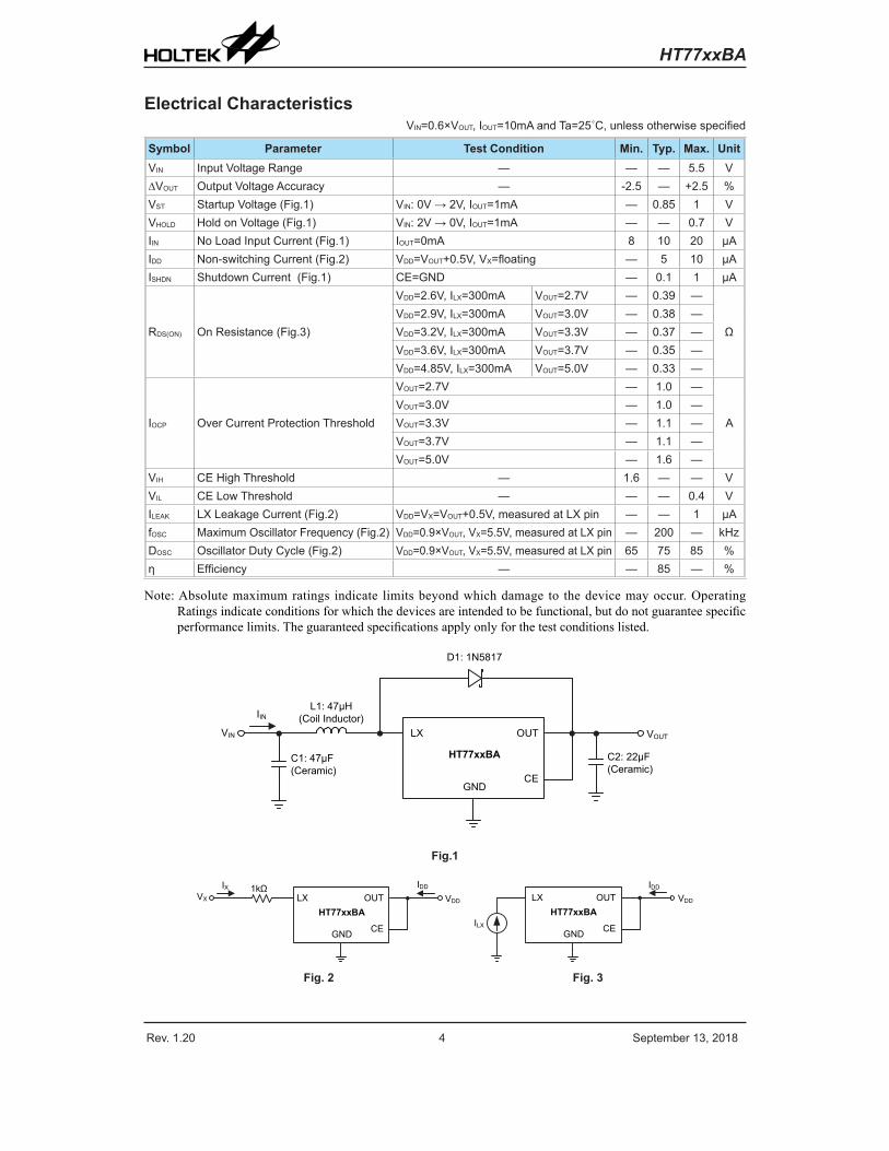
Electrical CharacteristicsVIN=0.6×VOUT, IOUT=10mA and Ta=25˚C, unless otherwise specified
Symbol Parameter Test Condition Min. Typ. Max. UnitVIN Input Voltage Range — — — 5.5 V∆VOUT Output Voltage Accuracy — -2.5 — +2.5 %VST Startup Voltage (Fig.1) VIN: 0V → 2V, IOUT=1mA — 0.85 1 VVHOLD Hold on Voltage (Fig.1) VIN: 2V → 0V, IOUT=1mA — — 0.7 VIIN No Load Input Current (Fig.1) IOUT=0mA 8 10 20 μAIDD Non-switching Current (Fig.2) VDD=VOUT+0.5V, VX=floating — 5 10 μAISHDN Shutdown Current (Fig.1) CE=GND — 0.1 1 μA
RDS(ON) On Resistance (Fig.3)
VDD=2.6V, ILX=300mA VOUT=2.7V — 0.39 —
ΩVDD=2.9V, ILX=300mA VOUT=3.0V — 0.38 —VDD=3.2V, ILX=300mA VOUT=3.3V — 0.37 —VDD=3.6V, ILX=300mA VOUT=3.7V — 0.35 —VDD=4.85V, ILX=300mA VOUT=5.0V — 0.33 —
IOCP Over Current Protection Threshold
VOUT=2.7V — 1.0 —
AVOUT=3.0V — 1.0 —VOUT=3.3V — 1.1 —VOUT=3.7V — 1.1 —VOUT=5.0V — 1.6 —
VIH CE High Threshold — 1.6 — — VVIL CE Low Threshold — — — 0.4 VILEAK LX Leakage Current (Fig.2) VDD=VX=VOUT+0.5V, measured at LX pin — — 1 μAfOSC Maximum Oscillator Frequency (Fig.2) VDD=0.9×VOUT, VX=5.5V, measured at LX pin — 200 — kHzDOSC Oscillator Duty Cycle (Fig.2) VDD=0.9×VOUT, VX=5.5V, measured at LX pin 65 75 85 %η Efficiency — — 85 — %
Note: Absolute maximum ratings indicate limits beyond which damage to the device may occur. Operating Ratings indicate conditions for which the devices are intended to be functional, but do not guarantee specific performance limits. The guaranteed specifications apply only for the test conditions listed.
LX OUT
GND
HT77xxBA
L1: 47μH(Coil Inductor)
D1: 1N5817
C1: 47μF(Ceramic)
C2: 22μF(Ceramic)
CE
VIN
IIN
VOUT
Fig.1
LX OUT
GND
HT77xxBA
1kΩ
CE
VX
IXVDD
IDDLX OUT
GND
HT77xxBA
CE
VDD
IDD
ILX
Fig. 2 Fig. 3
Rev. 1.20 5 September 13, 2018
HT77xxBA
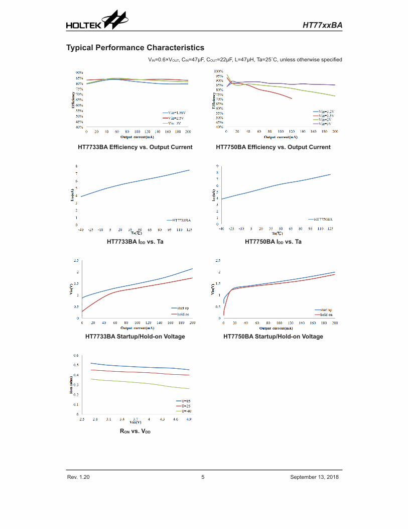
Typical Performance Characteristics VIN=0.6×VOUT, CIN=47µF, COUT=22µF, L=47µH, Ta=25˚C, unless otherwise specified
HT7733BA Efficiency vs. Output Current HT7750BA Efficiency vs. Output Current
HT7733BA IDD vs. Ta HT7750BA IDD vs. Ta
HT7733BA Startup/Hold-on Voltage HT7750BA Startup/Hold-on Voltage
RON vs. VDD
Rev. 1.20 6 September 13, 2018
HT77xxBA
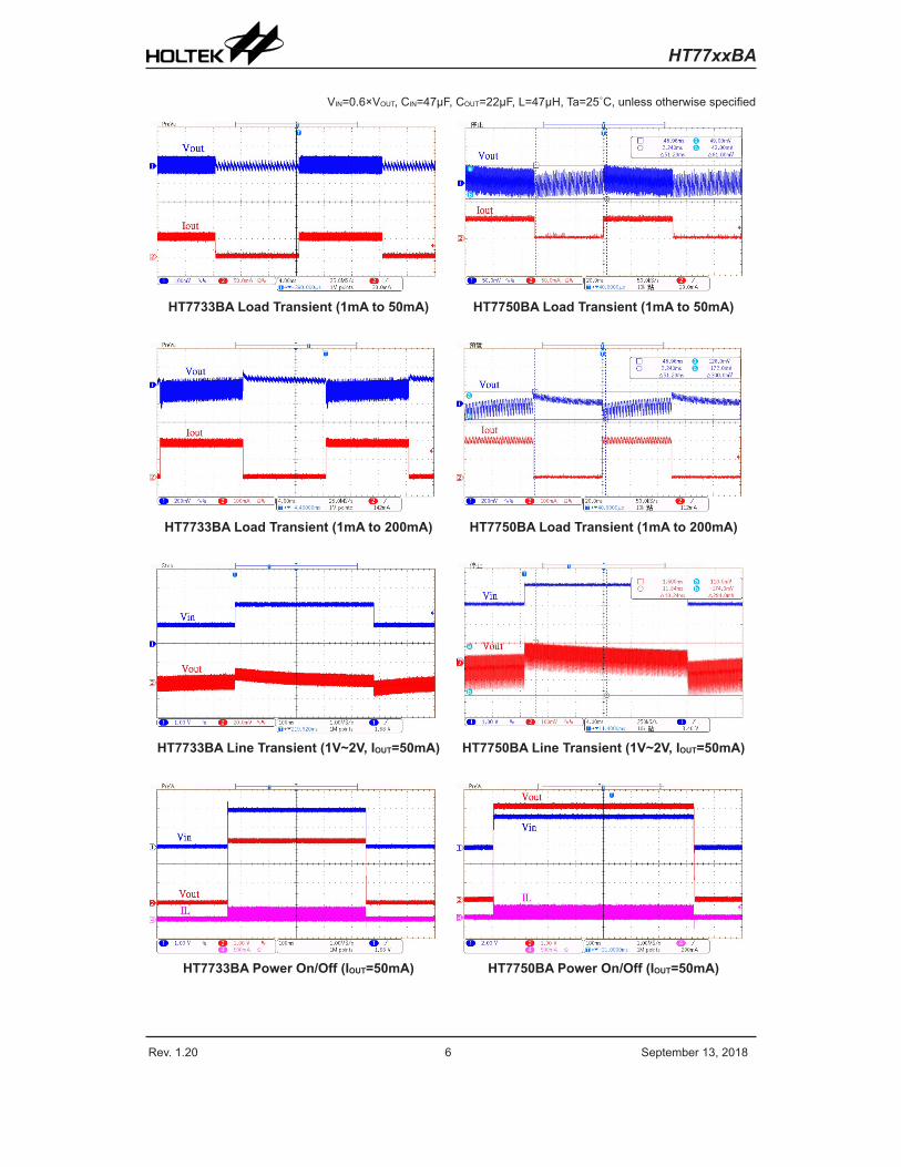
VIN=0.6×VOUT, CIN=47µF, COUT=22µF, L=47µH, Ta=25˚C, unless otherwise specified
HT7733BA Load Transient (1mA to 50mA) HT7750BA Load Transient (1mA to 50mA)
HT7733BA Load Transient (1mA to 200mA) HT7750BA Load Transient (1mA to 200mA)
HT7733BA Line Transient (1V~2V, IOUT=50mA) HT7750BA Line Transient (1V~2V, IOUT=50mA)
HT7733BA Power On/Off (IOUT=50mA) HT7750BA Power On/Off (IOUT=50mA)
Rev. 1.20 7 September 13, 2018
HT77xxBA
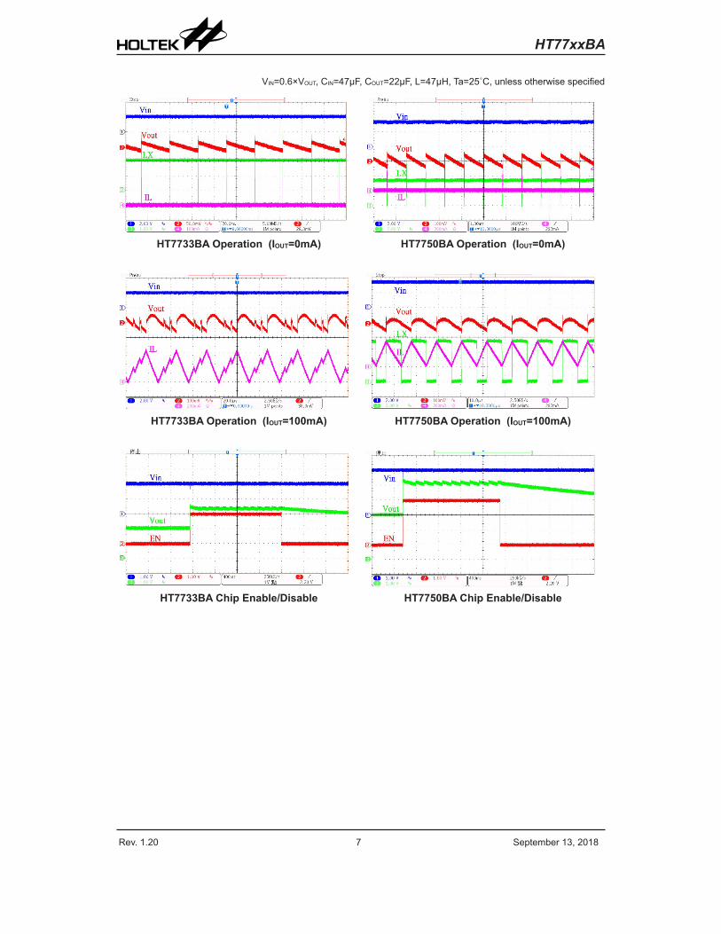
VIN=0.6×VOUT, CIN=47µF, COUT=22µF, L=47µH, Ta=25˚C, unless otherwise specified
HT7733BA Operation (IOUT=0mA) HT7750BA Operation (IOUT=0mA)
HT7733BA Operation (IOUT=100mA) HT7750BA Operation (IOUT=100mA)
HT7733BA Chip Enable/Disable HT7750BA Chip Enable/Disable
Rev. 1.20 8 September 13, 2018
HT77xxBA
Component Selection
Power InductorIt is recommended to use a 47μH or higher inductance to remain low output r ipple vol tage in most applications. Increasing the inductance will result in lower output ripple voltage. It is suggested to choose a lower DCR with a typical value less than 1Ω to reduce the efficiency loss. Otherwise, the chosen inductor saturation current should be greater than its peak current with a typical value of 1A or higher in applications.
Schottky DiodeThe diode breakdown voltage rating should be higher than the maximum output voltage. The diode current rating equal to or greater than 1A is suggested.
Input CapacitorA low ESR ceramic capacitor, CIN, is needed between the VIN and GND pins. Use ceramic capacitors with X5R or X7R dielectrics for their low ESRs and small temperature coefficients. For most applications, a 47µF capacitor will be a proper selection.
Output CapacitorThe output capacitor, COUT, selection is determined by the maximum allowable output voltage ripple. Use ceramic capacitors with X5R or X7R dielectrics for their low ESR characteristics. Capacitors in the range of 22μF to 100μF are a good starting point with an ESR of 0.1Ω or less. It is usually suggested to use a 22μF capacitor in most applications.
Ripple Improved Resistor with a No Load ConditionIt is strongly recommended to add a ripple improved resistor, R1, to keep the switching stability with a no load condition. It is recommended to set R1 to 0.15Ω. Note that this extra resistor improves the ripple performance under no load conditions, but induces higher ripple voltage when the load is heavy.
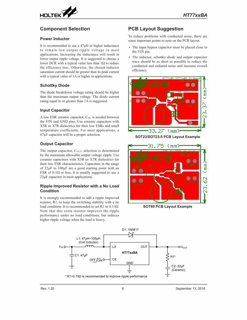
PCB Layout SuggestionTo reduce problems with conducted noise, there are some important points to note on the PCB layout.
• The input bypass capacitor must be placed close to the VIN pin.
• The inductor, schottky diode and output capacitor trace should be as short as possible to reduce the conducted and radiated noise and increase overall efficiency.
SOT23/SOT23-5 PCB Layout Example
SOT89 PCB Layout Example
LX OUT
GND
HT77xxBA
L1: 47μH~100μH(Coil Inductor)
D1: 1N5817
C1: 47μF
C2: 22μF(Ceramic)
R1*CEOFF ON
* R1=0.15Ω is recommended to improve ripple performance
VIN VOUT
Rev. 1.20 9 September 13, 2018
HT77xxBA
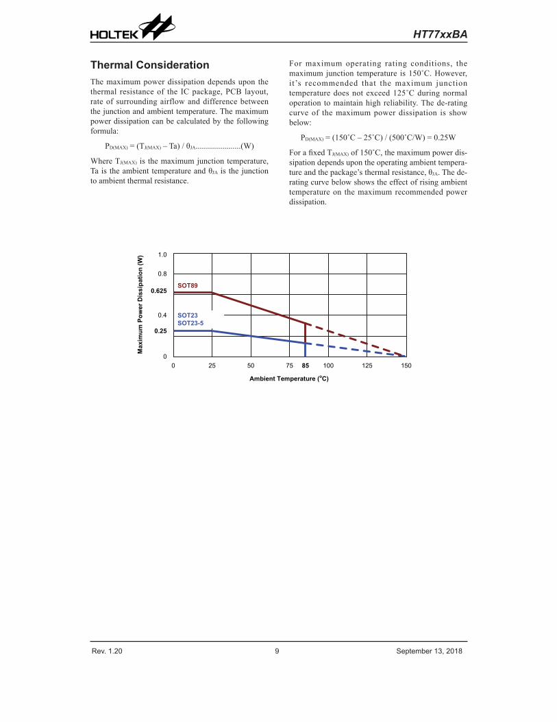
Thermal ConsiderationThe maximum power dissipation depends upon the thermal resistance of the IC package, PCB layout, rate of surrounding airflow and difference between the junction and ambient temperature. The maximum power dissipation can be calculated by the following formula:
PD(MAX) = (TJ(MAX) – Ta) / θJA......................(W)
Where TJ(MAX) is the maximum junction temperature, Ta is the ambient temperature and θJA is the junction to ambient thermal resistance.
For maximum operating rating conditions, the maximum junction temperature is 150˚C. However, it’s recommended that the maximum junction temperature does not exceed 125˚C during normal operation to maintain high reliability. The de-rating curve of the maximum power dissipation is show below:
PD(MAX) = (150˚C – 25˚C) / (500˚C/W) = 0.25W
For a fixed TJ(MAX) of 150˚C, the maximum power dis-sipation depends upon the operating ambient tempera-ture and the package’s thermal resistance, θJA. The de-rating curve below shows the effect of rising ambient temperature on the maximum recommended power dissipation.
25 50 75 100 1250
0.25
0.4
0.8
0
Ambient Temperature (oC)
Max
imum
Pow
er D
issi
patio
n (W
)
SOT23SOT23-5
85
1.0
150
0.625SOT89
Rev. 1.20 10 September 13, 2018
HT77xxBA
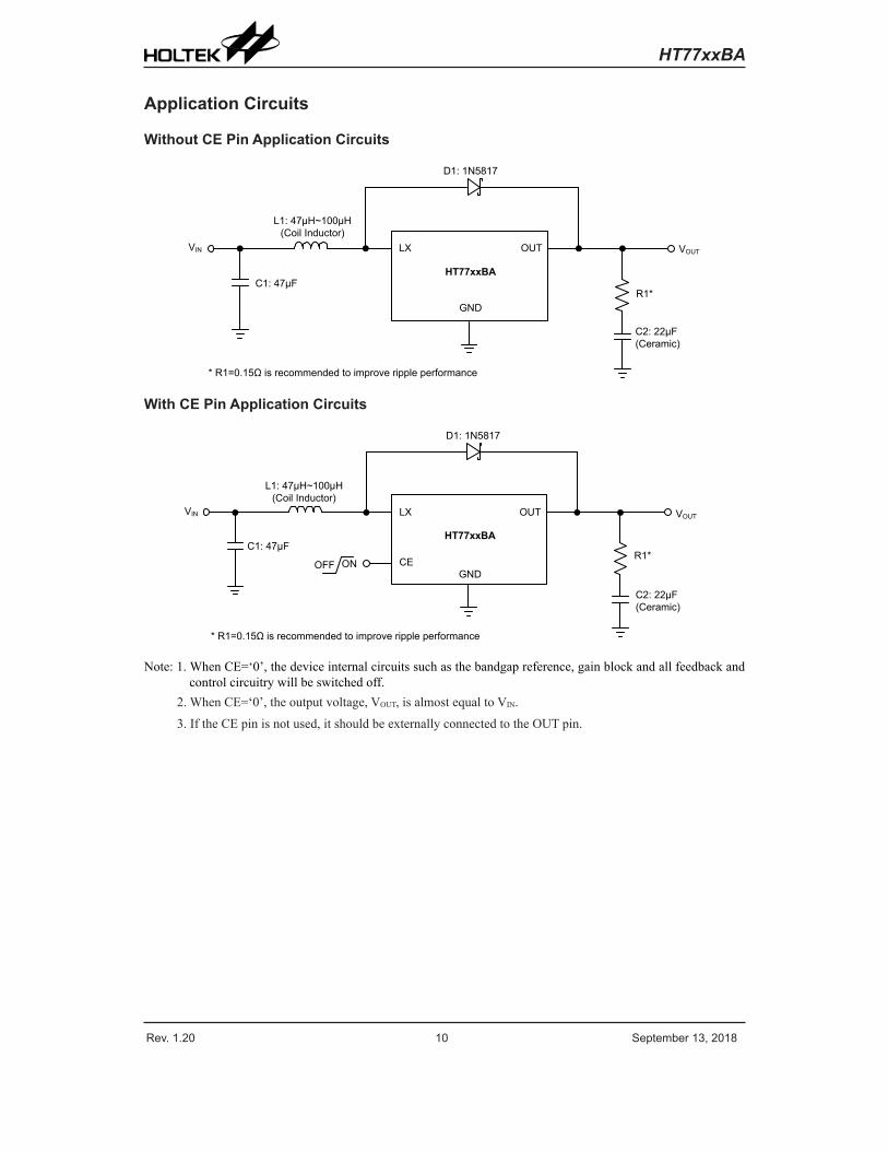
Application Circuits
Without CE Pin Application Circuits
LX OUT
GND
HT77xxBA
L1: 47μH~100μH(Coil Inductor)
D1: 1N5817
C1: 47μF
C2: 22μF(Ceramic)
R1*
* R1=0.15Ω is recommended to improve ripple performance
VIN VOUT
With CE Pin Application Circuits
LX OUT
GND
HT77xxBA
L1: 47μH~100μH(Coil Inductor)
D1: 1N5817
C1: 47μF
C2: 22μF(Ceramic)
R1*CEOFF ON
* R1=0.15Ω is recommended to improve ripple performance
VIN VOUT
Note: 1. When CE=‘0’, the device internal circuits such as the bandgap reference, gain block and all feedback and control circuitry will be switched off.
2. When CE=‘0’, the output voltage, VOUT, is almost equal to VIN.
3. If the CE pin is not used, it should be externally connected to the OUT pin.
Rev. 1.20 11 September 13, 2018
HT77xxBA
Package Information
Note that the package information provided here is for consultation purposes only. As this information may be updated at regular intervals users are reminded to consult the Holtek website for the latest version of the package information.
Additional supplementary information with regard to packaging is listed below. Click on the relevant section to be transferred to the relevant website page.
• Further Package Information (include Outline Dimensions, Product Tape and Reel Specifications)
• Packing Meterials Information
• Carton information
Rev. 1.20 12 September 13, 2018
HT77xxBA
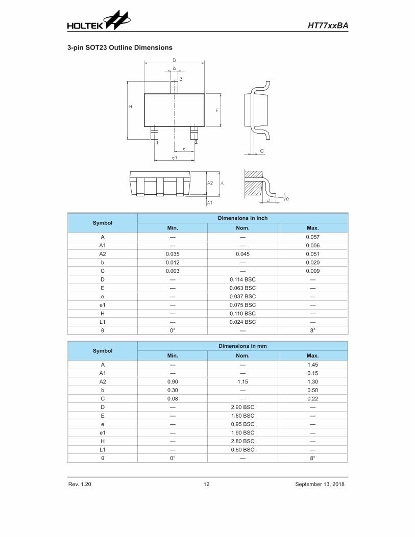
3-pin SOT23 Outline Dimensions
SymbolDimensions in inch
Min. Nom. Max.A — — 0.057
A1 — — 0.006A2 0.035 0.045 0.051b 0.012 — 0.020C 0.003 — 0.009D — 0.114 BSC —E — 0.063 BSC —e — 0.037 BSC —
e1 — 0.075 BSC —H — 0.110 BSC —L1 — 0.024 BSC —θ 0° — 8°
SymbolDimensions in mm
Min. Nom. Max.A — — 1.45
A1 — — 0.15A2 0.90 1.15 1.30b 0.30 — 0.50C 0.08 — 0.22D — 2.90 BSC —E — 1.60 BSC —e — 0.95 BSC —
e1 — 1.90 BSC —H — 2.80 BSC —L1 — 0.60 BSC —θ 0° — 8°
Rev. 1.20 13 September 13, 2018
HT77xxBA
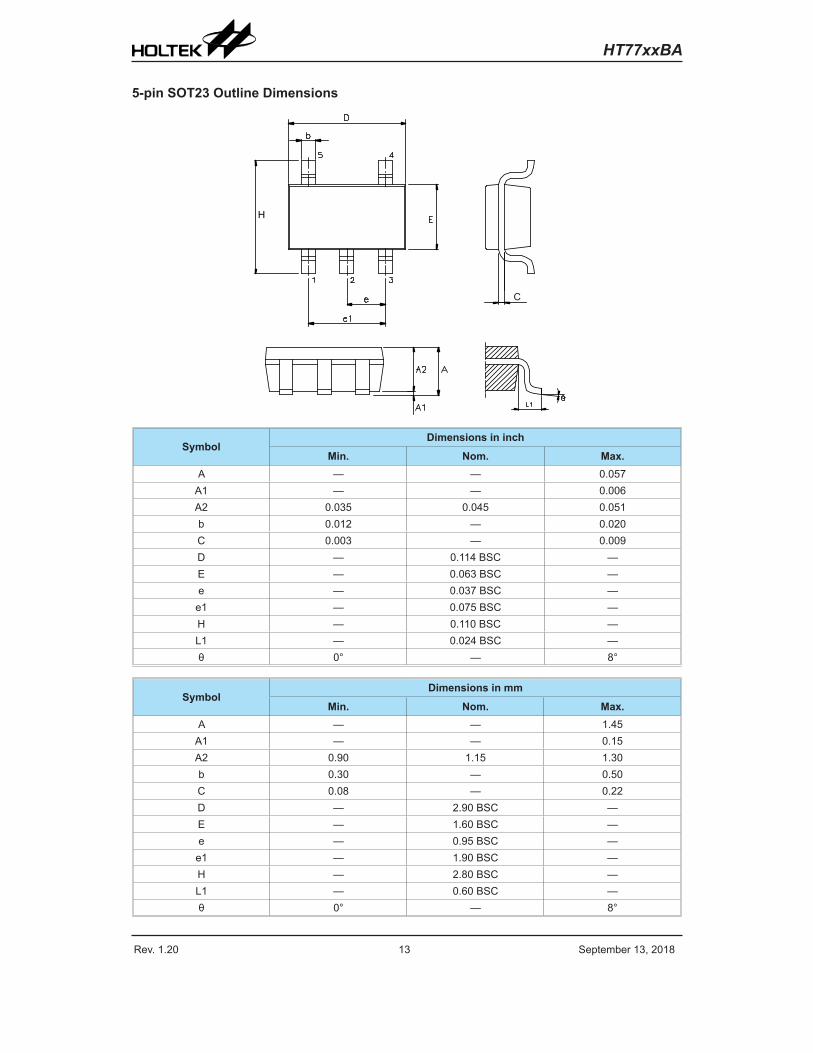
5-pin SOT23 Outline Dimensions
H
SymbolDimensions in inch
Min. Nom. Max.A — — 0.057
A1 — — 0.006A2 0.035 0.045 0.051b 0.012 — 0.020C 0.003 — 0.009D — 0.114 BSC —E — 0.063 BSC —e — 0.037 BSC —
e1 — 0.075 BSC —H — 0.110 BSC —L1 — 0.024 BSC —θ 0° — 8°
SymbolDimensions in mm
Min. Nom. Max.A — — 1.45
A1 — — 0.15A2 0.90 1.15 1.30b 0.30 — 0.50C 0.08 — 0.22D — 2.90 BSC —E — 1.60 BSC —e — 0.95 BSC —
e1 — 1.90 BSC —H — 2.80 BSC —L1 — 0.60 BSC —θ 0° — 8°
Rev. 1.20 14 September 13, 2018
HT77xxBA
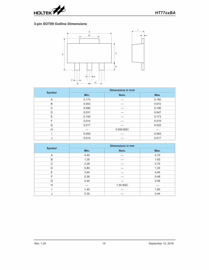
3-pin SOT89 Outline Dimensions
SymbolDimensions in inch
Min. Nom. Max.A 0.173 — 0.185 B 0.053 — 0.072 C 0.090 — 0.106 D 0.031 — 0.047 E 0.155 — 0.173 F 0.014 — 0.019 G 0.017 — 0.022H — 0.059 BSC —I 0.055 — 0.063J 0.014 — 0.017
SymbolDimensions in mm
Min. Nom. Max.A 4.40 — 4.70B 1.35 — 1.83C 2.29 — 2.70D 0.80 — 1.20E 3.94 — 4.40F 0.36 — 0.48G 0.44 — 0.56 H — 1.50 BSC —I 1.40 — 1.60 J 0.35 — 0.44
Rev. 1.20 15 September 13, 2018
HT77xxBA
Copyright© 2018 by HOLTEK SEMICONDUCTOR INC.
The information appearing in this Data Sheet is believed to be accurate at the time of publication. However, Holtek assumes no responsibility arising from the use of the specifications described. The applications mentioned herein are used solely for the purpose of illustration and Holtek makes no warranty or representation that such applications will be suitable without further modification, nor recommends the use of its products for application that may present a risk to human life due to malfunction or otherwise. Holtek's products are not authorized for use as critical components in life support devices or systems. Holtek reserves the right to alter its products without prior notification. For the most up-to-date information, please visit our web site at http://www.holtek.com.


![Asynchronous Transfer Mode - ATMcgi.di.uoa.gr/~istavrak/courses/CN-1/slide05[1].5.pdf · Asynchronous Transfer Mode - ATM ATM Forum →σχεδιασµός του ΑΤΜ εκδίδει](https://static.fdocument.org/doc/165x107/5fa031dcde52683ac8467d14/asynchronous-transfer-mode-istavrakcoursescn-1slide0515pdf-asynchronous.jpg)