Three-dimensional magnetic field sensor in IBM 0.18μm CMOS ...
7/26/2019 A 1V, 2.4GHz Fully Integrated LNA Using 0.18μm CMOS Technology
http://slidepdf.com/reader/full/a-1v-24ghz-fully-integrated-lna-using-018m-cmos-technology 1/4
A lV , 2.4GHz
Fully Integrated
LNA
Using
0.18pm
CMOS Technology
Lilo Zheiying, S.C.Rustngi’,
A F.
Li, ong Linn
Signal Processing and VLSI Design Lab, Department of Electrical and Computer Engineering
National University of Singapore, Singapore
1
19260
*
Institute of Microelectronics, Singapore 117685
Correspondence Author: Professor M .F. Li elelimf @us.e du.sg
A B S T R A C T
A
11:
?.4GHz fully integi-ated CMOS Low Noise
Amplifier (LNA) including the
500
referenced input
output matching ne tworks is implemented using
0. Spin
technology within a chip area of 4.1m m2. The amplifier
h k h e n o ise f ig u re
NF)
f 3.8dB and a forward gain
of
more tlian ZOdB. The details of the LNA analysis and
design procedure are presented in this paper.
1. INTRODUC.I’ION
The first stage of a wireles s receiver is typically an
LNA, whose main fun ction is
to
provide enough gain to
~ v e r c o m ehe noise of subsequent stages. Many LNA
designs are published so’farl
most
of them use off-chip
n ewo rk [3] or bolid wire inductor [GI to accomplish the
matching. In this paper,
a
fully integrated CMOS LNA
without off-chip matching network is proposed. Section
2
provides the detail design procedures and the
measurement sesultq are shown in section
3
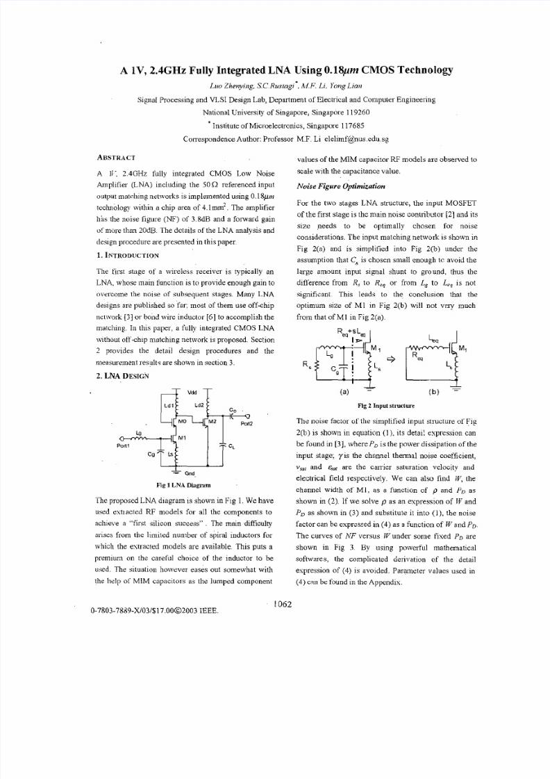
2.
LNA DESI
cg
p*ucLig
1
LNAGnd.
ingmm
lhe proposed LNA diagram is shown in Fig
1.
We have
used extiacted RF models for all the components to
achieve a “first silicon success’’ The main difficulty
arises from the limited number of spiral inductors for
which the extracted models are available. This puts a
premium
on
the careful c hoice of the inductor to be
used. The situation however eases out somewhat with
the help
of
MIM capacitors
as
the lumped component
values of the M IM capacitor RF models ar e observed to
scale with the capacitance value.
Noise
Figure Optimization
For the two stages LNA structue, the input MOSFET
of the first stage is the main noise co nt nh to r
[ 2 ]
and its
size needs to be optimally chosen for noise
considera tions. The input match ing network is shown in
Fig 2(a) and is simplified into Fig
2 b)
under the
assumption that
C,
is chosen small enough tc avoid the
large amount input signal shunt to ground, thus the
diflerence from
R,
t o R e , or from Lx o L,, is not
significant. This leads to the conclusion that the
optimum
size
of MI in Fig
2 b)
will
not
vmy much
from that of MI in Fig 2(a).
A
--L
a)
-
@
-
Fig 2 Input
structwc
The noise factor of the simplified input structure of Fig
2(b)
is shown in equation
( I ) ,
its detail expression can
be found in
[3],
wh ereP D
is
the pow er dissipation of the
input stage; yis the channel themial noise coefficient,
v r v r and are the carrier saturation velocity and
electrical field respectively. We can also find
W
the
channel width of MI, as a function of p and P D as
shown in ( 2 ) .
f
we
solve p
as an expression of CV and
PD as shown in
(3)
and substitute it into
( I ) ,
the noise
factor can be exprzssed in
(4)
as
a
function of W and
PD.
The curves of
NF
versus Wunder some f ixed
PD
are
shown in Fig 1. By using powerful mathematical
softwares, the complicated delivation of the detail
expression of (4) is avoided. Parametel- values used in
( 4 ) c m be found in the Appendix.
1062
0-7803-7Sd9-X/03/$17.00~2003 EEE.

7/26/2019 A 1V, 2.4GHz Fully Integrated LNA Using 0.18μm CMOS Technology
http://slidepdf.com/reader/full/a-1v-24ghz-fully-integrated-lna-using-018m-cmos-technology 2/4
p = ;(I+ .P, 1
)r,J L
.F
= I
+ - e P (II'.
P,
3> *2
(3)
(4)
I t
is
clear from Fig
3
that for every given PD here
is a
corresponding optimum value of K which yields the
minimum noise figure. In this LNA design,
PD
is
specified as 4.51nW (the solid line) and the optimum
value of W is around 250prrr. The selection of W is a
trade-off between the available
RF
models and the
optimum noise figure, thus
l,P
of 1 S O p s chosen for
which the extracted
RF
models were available. In this
I+
range, the noise figure does not deteriorate
significantly
Fig
3
N F
vs. W
Pi
LNA
nput stage
Thc cascodc device MO "shields" M I from signal
variations at its drain and greatly reduces p121 hus the
LNA can'he t reated approsimatek
a s
a unilateral design
pl+O)
[A].
In this way
MO
reduces the interaction
of
the tuned output with the tuned iiiput that facilitates the
matching task. Chan icl width of
MO is
simply chosen
the samr size as MI;
150pr1
to provide the 4.SmW
power dissipation o ft he input stage.
Input matching
'The input matching netwoi-k is shown in Fig 4. L,, L,
and MI constiuct a source degeneration stage [SI
without C the input impedance is:
In (5 ) ;L, is chosen to mak e the real part of Zit, to match
the signal source resistance and Lx elves the role of
canceling the imaginary part
of Z,,,.
However, that's not
alwnys true while' Ls and L, can not be tuned
continuously. In this case, capacitor C is connected
between the gate of M I and ground to give another
order of freedom of tuning Z as shown in the
approximated expression of
6).
Note that if C, is small
enough to be neglected, Z n (6) will shrink back to the
espression
5).
7)
Linearity consideration
One of the advantages of two stages amplifier is'that i t
separates the optimization tasks of noise, linearity
perfomance and input , output matching while, for
single stags LNA; they need to be considered
simultaneously. In a cascade structure, P3 of the last
stage is the prominent facto r of the total
IP3
[l][2], thus
M2 contributes more to the LNA linearity than M1
IIP3 of M2 can be written as
(7) [7],
where B is the
normal field mobility degradation factor.
7)
shows that
IIP3 of
the second stage can be enhan ced by increasing
J i , ,
for this reason the gate of M2 is connected to
J/,
through Ldl to give
V x J ~
he maximum value. However.
it increases the power dissipation as we ll; channel width
of M2 n eeds to be reduced to compensate this problem.
Foitunately, ieducing the channel width
of M2
will not
affect the lineaiity significantly, thus
a
small device
with relatively high
J
is the way used hei-e to impro ve
linearity
of
the LNA [?]
Ontput mutching
Making output matching is more complicated than the
input one because the output impedance is vel?
sensitive to the component values. L',,
is
the load
inductor of the first stage, however i t affects the output
impedance significantly. As show n in the se tup in Fig
5 ,
R,
is
the output 1-esistance ooking into the drain of M2.
If the value of
Ldl
is chose n improperly,
R,
will become
negative at the desired resonant frequency and thus
introduces the instable factor:
&+-I.
We can get a
more intuitive view from the simulation result in Fig
6.
At the frequency
of
2.40Hz , i f Ld
is
given a value of
4nH.
R,
is negative.' In auother two cases, when Ldl is
chosen InH or S nH , R , becomes positive.
. .
1063
7/26/2019 A 1V, 2.4GHz Fully Integrated LNA Using 0.18μm CMOS Technology
http://slidepdf.com/reader/full/a-1v-24ghz-fully-integrated-lna-using-018m-cmos-technology 3/4
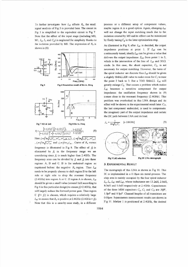
To
fuither investigate how
Ldl
affects
,
the small
signal analysis of Fig 5 is provided here. The circuit in
Fig
5 is simplified to the equivalent circuit in
Fig
7 .
Note that the effect of the input stage (including MO,
MI:
L,,
L, and
C,)
is neglected for simplicity thanks to
the isolation provided by MO. The expression
of
R ,
is
shown in 8):
0 2 4 8
1 2
9 6
Freq
(GHz)
Fig 5
Fig 6Simuliltion result
of Ra
VS.
Req
Fig 7
h12 U Fig 8 Ro
vs
Freq
process
or
a different setup of component values,
maybe region A is a good option. Again, changing L d 1
will not change the input matching much due to the
isolat ion created by MO and its effect can he m inimized
by finely tuning
C,
in the later opt imizat ion step.
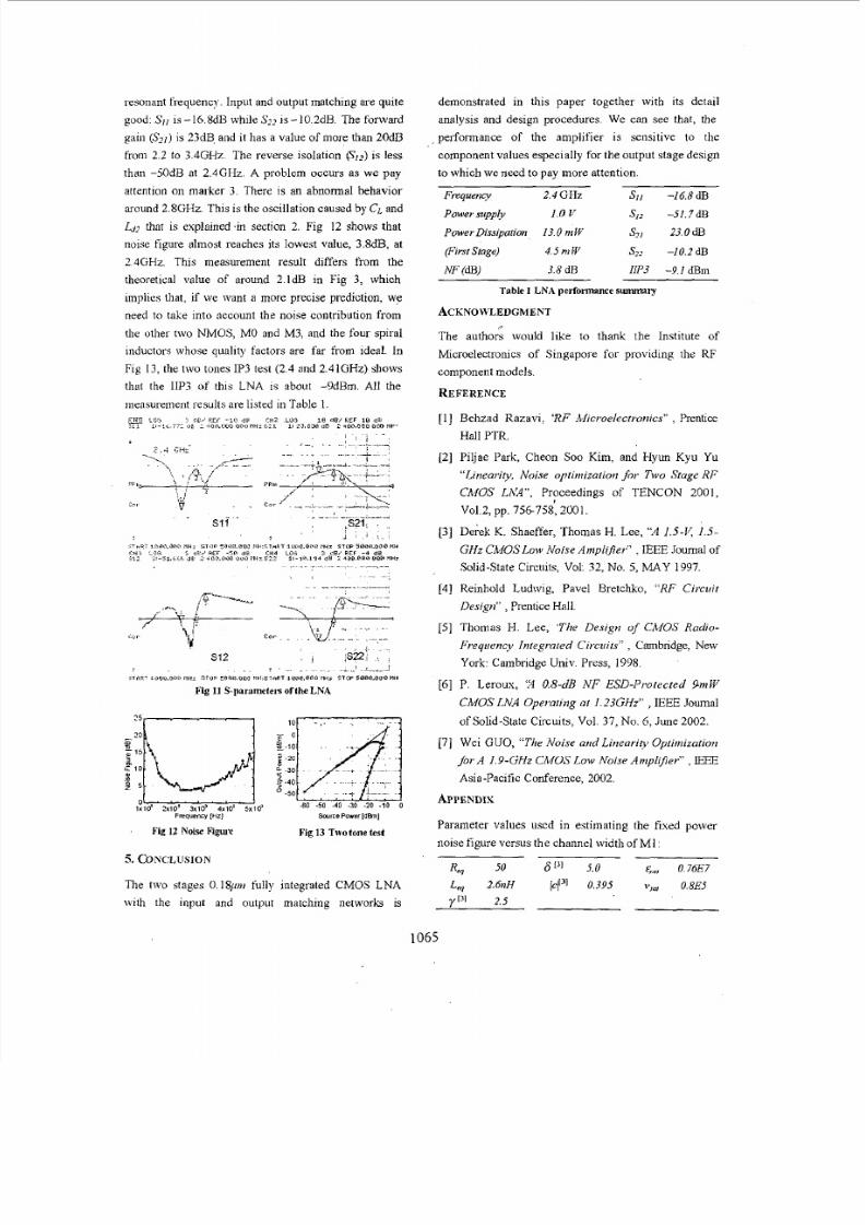
As
illustrated in
Fig
9,
after Ldl
is
decided , the output
impedance posi t ions at point I . If L d 2 can he
continuously tuned, ideally
L d z
can he given a value that
de l ivers the output impedance Z f rom point
1
to
3 ,
which is the intersect ion of the l ine of
Ld j
and 50Q
circle. In this case, the shunt capaci tor , CL, is not
necessary for output matching. However, the turns of
the spiral inductor are discrete thus La should he given
a slightly SMALLER value to make room for
C
to.tune
the point 2 hack to 3. But a TOO SMALL Ld.' will
greatly enlarge CL. hat causes a problem which makes
LQ becomes a sensi t ive component for output
impedance: the osci l lat ion frequency shown in 9)
comes close to the resonant frequency
(2 .4GHz) .
This
problem was overlooked in this
LNA
des ign and
its
effect will he shown in the experimental result later.
CO,
the last component undecided, is used to compensate
the ima gina q par t of the output impedance and i sola te
the DC path be tween LN A and i t s load.
. =r
p - ( f / x f J p - ( J / L f
Wro
8)
p x
, *- a
l - i / /~ )~~+~- ( / /~ ) *~ i / / .~~
- if /X
IMere
.r;-Jzn~~, c~,;+c,,+c,~,,c,)
f, JbJ
, j 2 n K
nd
J
/2m;,C,: .
Curve of
R
versus
b
frequencv is illustrated in Fig 8. The effect of
eliminated by ,6 in the frequency range we
are
~-
is
& A/
consideling since
f is
much higher than 2.4GHz. The
frequency axes can he divided by
fi
and
h
nto three
regions: A: B and C. B
is
: le und esire d reg ion
a s
mentioned before: the negative
R ,
region. Thus
Ldl
needs
to
he properly chosen to shift region
B
to the left
side or right side to drop the resonant frequency
(2 .4GHz) into
region A or
C .
If region
A is
chosen,
Ldl
should he given a smal l va lue (a round In H according to
Fig 6 in this part icular design) to ensurefi>2 .4GHz , that
\ ,ill largely reduce the forward power gain. T hus region
C i
is
chosen; which requires a relatively large
Ldl
to ensure that
R ,
is positive at 2.4GHz (2.4GHz
>h .
Note that this
is
a case-hycase study, in a different
Fig 9 Mlselection
Fig 10
LNA
ndc ph
3
E~~~~~~~~~~~
R ~ ~ ~ , ~
Th e micrograph of this L NA is shown in
k ig 10.
This
IC is implemented in a
0.18pni
six metal process. The
chip area is mainly occupied by the four spiral inductor
Ls,
L,,
L d 1
and
L a ,
whose inductance are 13.2n H, 2.6nH,
8 .3nH a nd
1 6nH
respectively at
2.4GHz.
Capacitances
of the three MIM capaci tors
C,, C L
and
CO
are j O f F
1.9pF and 0.9pF. Channel lengths of all transistors are
0 18pni S-parameten measurem ent resul ts are shown in
Fig
11.
Marker 1
is
posi t ioned' at 2 .4GHz, the desired
1064
7/26/2019 A 1V, 2.4GHz Fully Integrated LNA Using 0.18μm CMOS Technology
http://slidepdf.com/reader/full/a-1v-24ghz-fully-integrated-lna-using-018m-cmos-technology 4/4
resonant frequency. Input and output matching are quite
good: S I , is-16.8dB while
S?..
i s - l 0 .2d B. The fo rw ad
gain
( I )
is 23dB, and it has a value of m ore than 20d B
f~-oni
.2
to 3.4GHz. The reverse isolation
@ I I I is
less
than -5OdB at 2.4GH z. A problem occurs as we pay
attention
on
marker
3.
There is an abnormal behavior
around
2.8GHz.
This
is
the oscillation caus ed by
C
and
Li12 that
is
explained .in section 2. Fig 12 shows that
noise figure ahnost reaches its lowest value, 3.8dB, at
2.4GHr.
This measurement result differs from the
theoretical value of around 2. ld B in Fig 3, which
implies that, if we want a mol-e precise prediction, w e
need
to
take into account the noise contribution from
the other two NMOS, MO and M3, and the four spiral
inductors whose quality fac tors are far
f~ -o m
deat.
In
Fig
13 ,
the
two
tones IP3 test
( 2 .4
and 2.41GHz) show s
that the IIP3 of this LNA
is
about -9dBm.
All
the
meesurement resu lts are listed in Table
1
5 8 dB/
*FF 10 db
I W d B 2
q86.088 [ioa
nr-
E E i
p *OB.’
Fig
12
Noise
Figulur
Fig 13 Two tone
l e s t
5 CONCLIISION
The two stages 0 .18p~ully integrated CMOS LNA
with the input and output matching networks is
demonstrated in this paper together with its detail
analysis and design procedures. We ciin see that, the
,performance of the amplifier is sensit ive to the
com ponent values especially for the output stage design
to which we need to pay m ore attention .
Fmquency
2.4
GH2
S I I
-16.8dB
Power supply
1.0
v
S,i -51.7dB
Power issiparion 13.0nmW SZI
23.0
dB
(First fnge)
4 . 5 n i R Sa
-1O.ZdB
NF (a)
3.6
dB
IIP3 -9.1
dBm
Table 1
LNA p e r f o mme summaly
ACKNOWLEDGMENT
The authors would like to thank the Institute of
Microelectronics of Singapore for pioviding the RF
component models.
REFERENCE
[ I ] Behzad Razavi, ‘RF .hlcroe/ecti-oriics” , Prentice
Hall
PTR.
[2] Piljae Park, Cheon So0 Kim, and Hyun Kyu Yu
“Linenrip Noise optiniizntiori
for Two
Stage RF
CMOS LAY”,
Proceedings of TENCON 2001,
vo1.2, pp. 756758,2001
[3]
Derek
K.
Shaeffer, Thomas
H.
Lee,
“A
1.5-1.:
1.5-
GHz CMOS Low N oise Amplifier” , EEE Journal of
Solid-State Circuits, Vol: 32, No. 5 , M A Y 1997.
[4]
Reinhold Ludwig, Pave1 Bretchko,
“RF Circuir
Desigri”
,
Prentice Hall.
[SI
Thomas
H.
Lee,
Tlie Des i gn o/
CMOS Radio-
Frequency Integrared Circuits“
,
Cambridge, New
York: Cambridge Univ. Press, 1998.
[6] P. Leroux, 2 0.8-dB NF ESD-Protec ted PniW
CMOS LNA Oper,nririg
at
I.23GHz”
, EEE Journal
of Solid-State Circuits, Vol. 37, No. 6, June 2002.
[7] Wei
GUO,
“Tlie
Noise
mid
Linearip Opfiniizntion
j orA
1.9-GHz CMOS Low Noise Amnplifier” ,
EEE
Asia-Pacific Conference, 2002.
APPENDIX
Parameter values used in estimating the fixed power
noise figure versus the channe l width of
M I
:
Reg
50 6 0 1 5.0 , 0.76E7
L ,
2.6nH lcf3]
0.395 v ~
0.8E5
y” I 2.5
1065


![) and K · f1(1285)! a0(980)ˇ decay: formalism Vertices: f1 K (K 1) K (K).. it1 = igf1C1ϵ ϵ′ gf1 = 7555 MeV, evaluated as the residue at the pole of T = [1 VG] 1V for K K c:c:](https://static.fdocument.org/doc/165x107/5f08d6ad7e708231d423f7ef/-and-k-f11285-a0980-decay-formalism-vertices-f1-k-k-1-k-k-it1-.jpg)
![A 1V 14b Self-Timed Zero- Crossing-Based Incremental ΔΣ ADC[1] Class Presentation for Custom Implementation of DSP By Parinaz Naseri Spring 2013 1.](https://static.fdocument.org/doc/165x107/56649f0c5503460f94c20230/a-1v-14b-self-timed-zero-crossing-based-incremental-adc1-class-presentation.jpg)