TKT-3500 Microcontroller · PDF fileTKT-3500 Microcontroller systems Lec 6 ... Symbol R; unit...
87
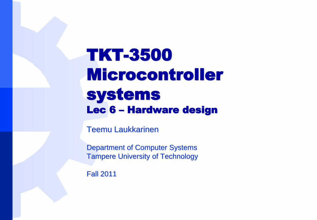
TKT-3500 Microcontroller systems Lec 6 – Hardware design Teemu Laukkarinen Department of Computer Systems Tampere University of Technology Fall 2011
Transcript of TKT-3500 Microcontroller · PDF fileTKT-3500 Microcontroller systems Lec 6 ... Symbol R; unit...
TKT-3500
Microcontroller
systems
Lec 6 – Hardware design
Teemu Laukkarinen
Department of Computer Systems
Tampere University of Technology
Fall 2011
#2/42
Sources
Original slides by Erno Salminen
Robert Reese, Microprocessors: From Assembly
to C with the PIC18Fxx2, Charles River Media,
2005
Northwestern University mechatronics design wiki
http://hades.mech.northwestern.edu/wiki/index.php/Mai
n_Page
Wikipedia
#3/42
Contents
Recap: Basic electronics
Current, voltage, power
Ohm’s law, Kirchoff’s law
Resistor, capacitance, inductance
Semiconductors: diode, transistor, IC
Others: fuse, regulator, op. amp.
(Meters: multimeter, oscillator, signal
analyzer)
Packages and assembly
Circuit board design
#5/42
Current I
Current measures how many charge carriers
(electrons) flow through a conductor
Conductor is material that can conduct electrical current,
usually some metal such as aluminum or copper
Symbol I; unit Ampere, A
microcontroller systems operate with e.g. 10 mA – 500 mA
Current may flow only in a closed circuit
from positive voltage to negative
Direct current (DC) flows always in one direction
whereas alternating current (AC) varies
The origin of current is also called source whereas
the destination is called sink or drain
#6/42
Voltage U/V
Voltage means electrical potential –
difference in amount electrical charge –
between two points of a circuit
Symbol U (sometimes V); unit Volt, V
microcontrollers use e.g. 2-5 V
Voltage source Vs is a device that provides
current with (ideally) fixed voltage level
single AA battery provides 1.5 V, car battery 12 V
wall outlet 230V, 50Hz alternating current (AC)
In practice, large current causes voltage drop
#7/42
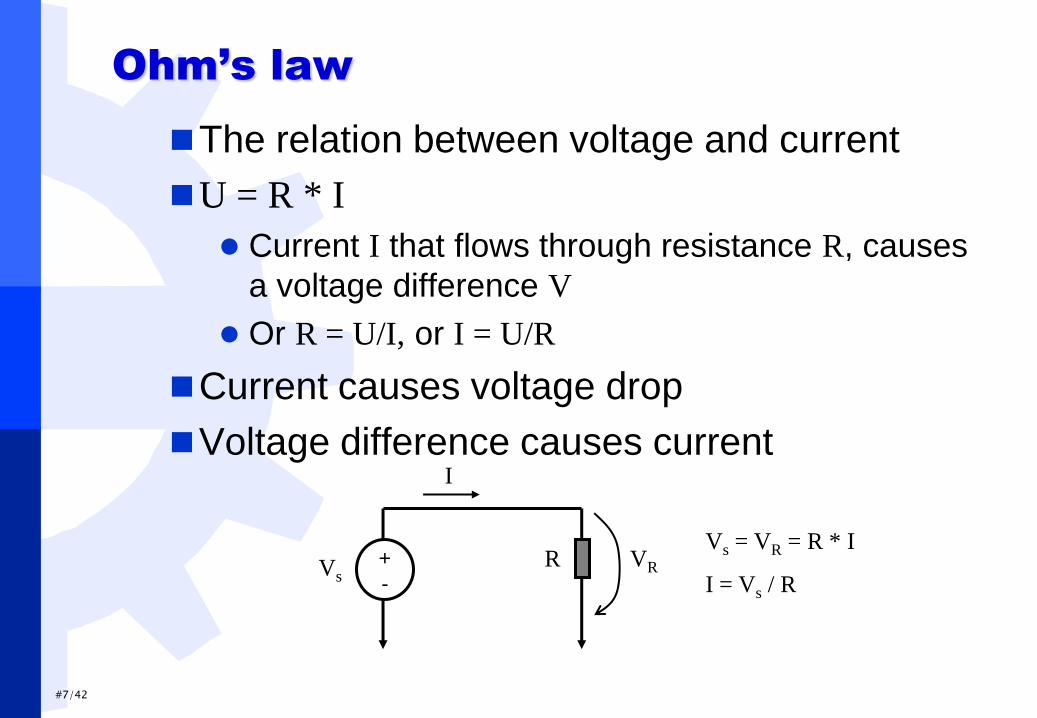
Ohm’s law
The relation between voltage and current
U = R * I
Current I that flows through resistance R, causes
a voltage difference V
Or R = U/I, or I = U/R
Current causes voltage drop
Voltage difference causes current
VR
I
+
- Vs
R
Vs = VR = R * I
I = Vs / R
#8/42
Power P and energy E
Power measures the amount of work done in unit time Rate of energy consumption
Symbol P; unit Watt, W
Product of voltage and current: P = U * I = U * (U/R)
PIC uses <1 W of power
Energy E means the total work Symbol E; unit Joule, J
E = P * t = (U*I) *t, where t denotes time
Sometimes given in Watt-hours, Wh or volt-Ampere-hours VAh
Battery stores some amount of energy E that is spent at certain rate P One AA battery contains 1000-3000 mAh
#9/42
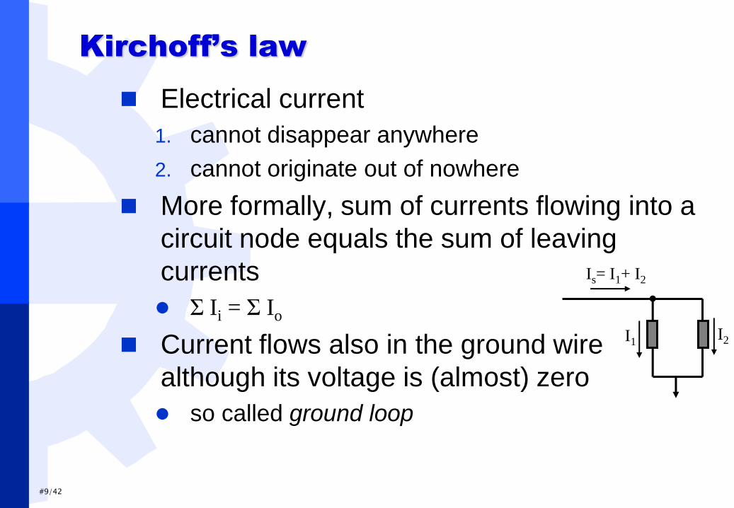
Kirchoff’s law
Electrical current
1. cannot disappear anywhere
2. cannot originate out of nowhere
More formally, sum of currents flowing into a
circuit node equals the sum of leaving
currents
Σ Ii = Σ Io
Current flows also in the ground wire
although its voltage is (almost) zero
so called ground loop
I1 I2
Is= I1+ I2
Basic passive
components
#11/42
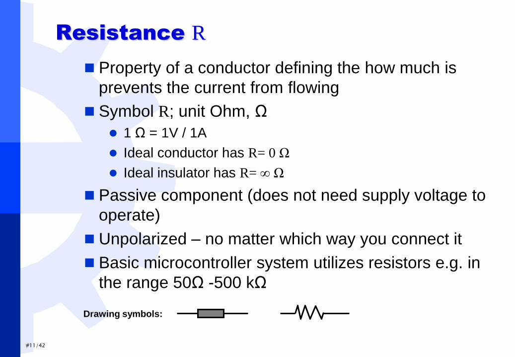
Resistance R
Property of a conductor defining the how much is
prevents the current from flowing
Symbol R; unit Ohm, Ω
1 Ω = 1V / 1A
Ideal conductor has R= 0 Ω
Ideal insulator has R= ∞ Ω
Passive component (does not need supply voltage to
operate)
Unpolarized – no matter which way you connect it
Basic microcontroller system utilizes resistors e.g. in
the range 50Ω -500 kΩ
Drawing symbols:
#12/42
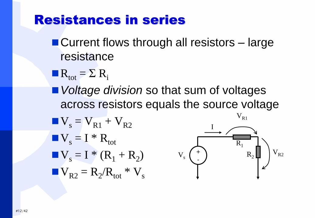
Resistances in series
Current flows through all resistors – large
resistance
Rtot = Σ Ri
Voltage division so that sum of voltages
across resistors equals the source voltage
Vs = VR1 + VR2
Vs = I * Rtot
Vs = I * (R1 + R2)
VR2 = R2/Rtot * Vs
VR2
I
+
- Vs
R2
R1
VR1
#13/42
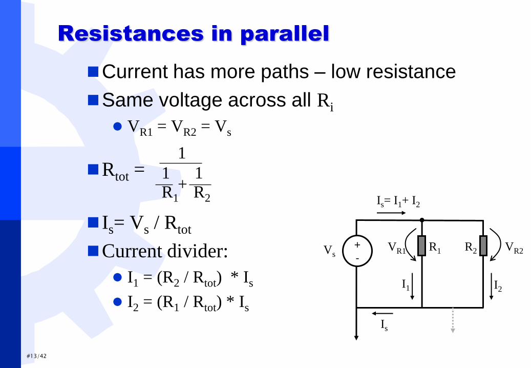
Resistances in parallel
Current has more paths – low resistance
Same voltage across all Ri
VR1 = VR2 = Vs
Rtot =
Is= Vs / Rtot
Current divider:
I1 = (R2 / Rtot) * Is
I2 = (R1 / Rtot) * Is
I1 I2
Is= I1+ I2
+
- Vs
VR1
1
+ 1 1 R1 R2
VR2 R2 R1
Is
#14/42
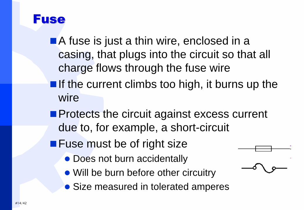
Fuse
A fuse is just a thin wire, enclosed in a
casing, that plugs into the circuit so that all
charge flows through the fuse wire
If the current climbs too high, it burns up the
wire
Protects the circuit against excess current
due to, for example, a short-circuit
Fuse must be of right size
Does not burn accidentally
Will be burn before other circuitry
Size measured in tolerated amperes
#15/42
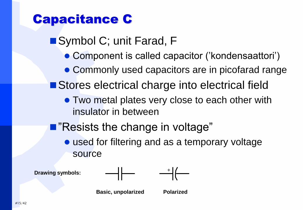
Capacitance C
Symbol C; unit Farad, F
Component is called capacitor (’kondensaattori’)
Commonly used capacitors are in picofarad range
Stores electrical charge into electrical field
Two metal plates very close to each other with
insulator in between
”Resists the change in voltage”
used for filtering and as a temporary voltage
source
Drawing symbols:
Basic, unpolarized Polarized
+
#16/42
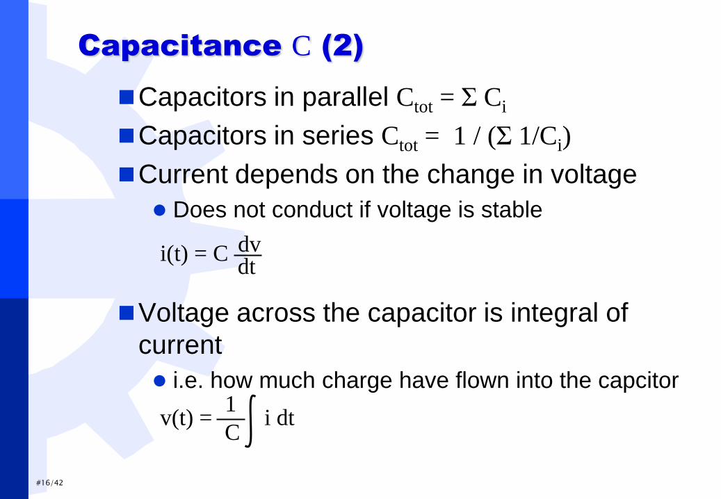
Capacitance C (2)
Capacitors in parallel Ctot = Σ Ci
Capacitors in series Ctot = 1 / (Σ 1/Ci)
Current depends on the change in voltage
Does not conduct if voltage is stable
Voltage across the capacitor is integral of
current
i.e. how much charge have flown into the capcitor
i(t) = C dv dt
v(t) = i dt 1
C
#17/42
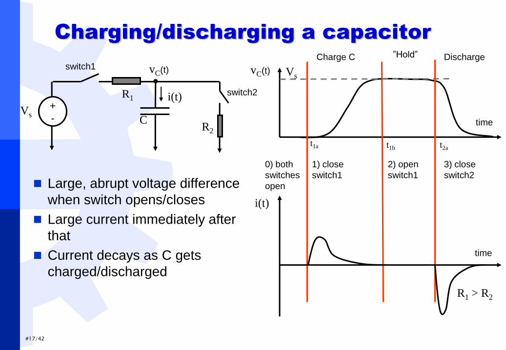
Charging/discharging a capacitor
Large, abrupt voltage difference
when switch opens/closes
Large current immediately after
that
Current decays as C gets
charged/discharged
i(t) +
- Vs
R1
vC(t) vC(t)
t1a
Vs
C R2
t2a t1b
switch1
switch2
0) both
switches
open
1) close
switch1
2) open
switch1
3) close
switch2
Charge C ”Hold” Discharge
i(t)
R1 > R2
time
time
#18/42
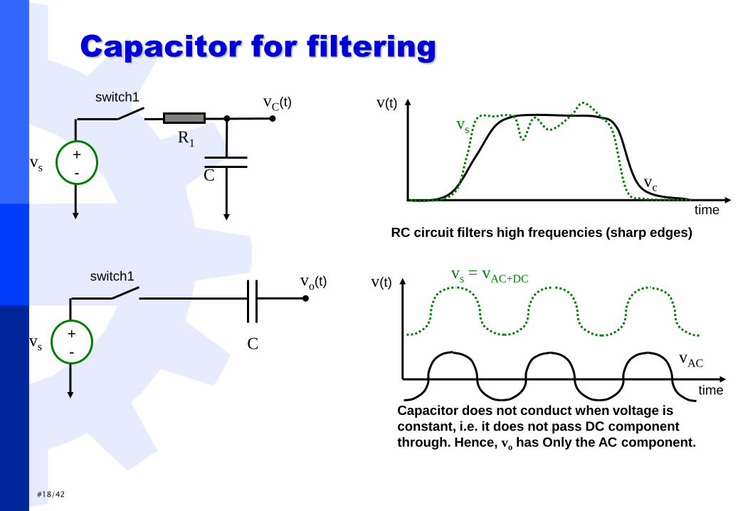
Capacitor for filtering
+
- vs
R1
vC(t)
C
switch1 v(t)
vs
time
vc
+
- vs
vo(t)
C
switch1 v(t) vs = vAC+DC
time
vAC
RC circuit filters high frequencies (sharp edges)
Capacitor does not conduct when voltage is
constant, i.e. it does not pass DC component
through. Hence, vo has Only the AC component.
#19/42
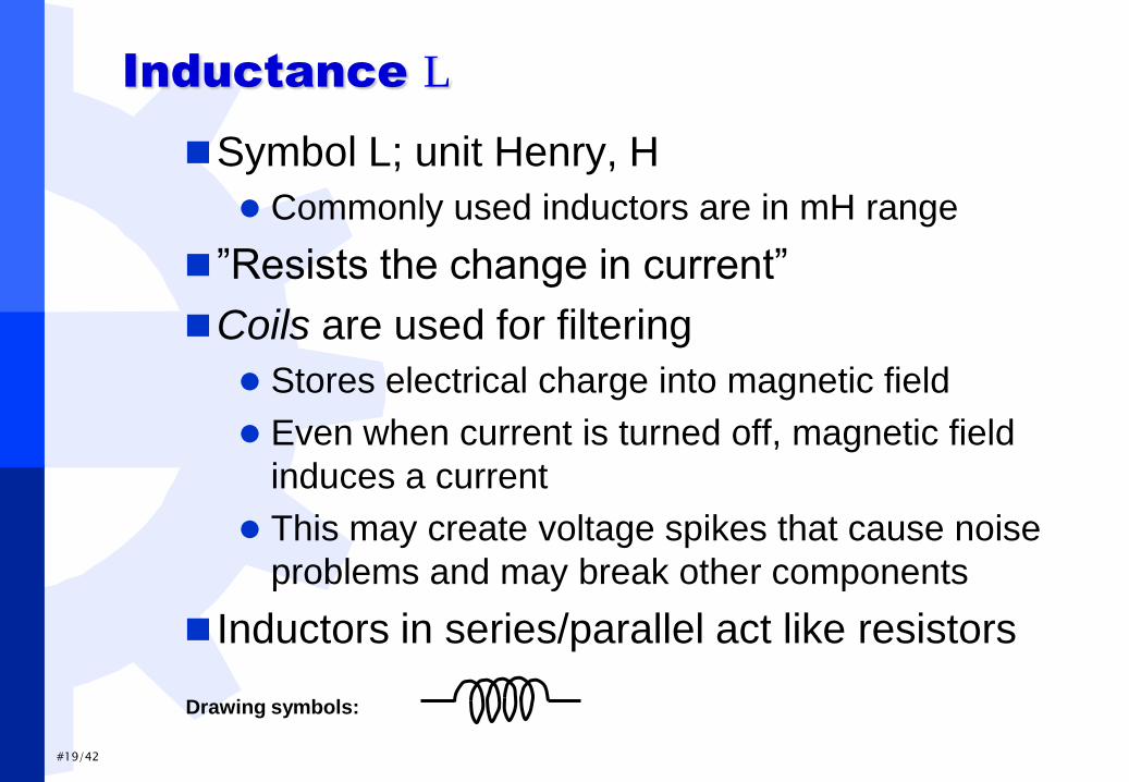
Inductance L
Symbol L; unit Henry, H
Commonly used inductors are in mH range
”Resists the change in current”
Coils are used for filtering
Stores electrical charge into magnetic field
Even when current is turned off, magnetic field
induces a current
This may create voltage spikes that cause noise
problems and may break other components
Inductors in series/parallel act like resistors
Drawing symbols:
#20/42
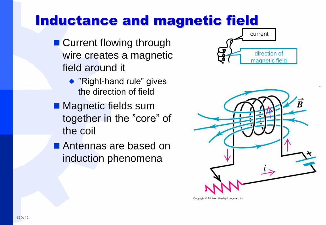
Inductance and magnetic field
Current flowing through
wire creates a magnetic
field around it
”Right-hand rule” gives
the direction of field
Magnetic fields sum
together in the ”core” of
the coil
Antennas are based on
induction phenomena
current
direction of
magnetic field
#21/42
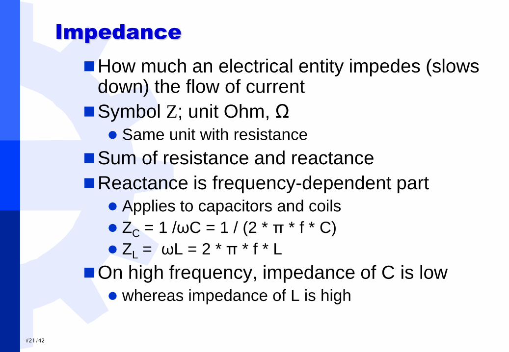
Impedance
How much an electrical entity impedes (slows down) the flow of current
Symbol Z; unit Ohm, Ω
Same unit with resistance
Sum of resistance and reactance
Reactance is frequency-dependent part Applies to capacitors and coils
ZC = 1 /ωC = 1 / (2 * π * f * C)
ZL = ωL = 2 * π * f * L
On high frequency, impedance of C is low whereas impedance of L is high
#22/42
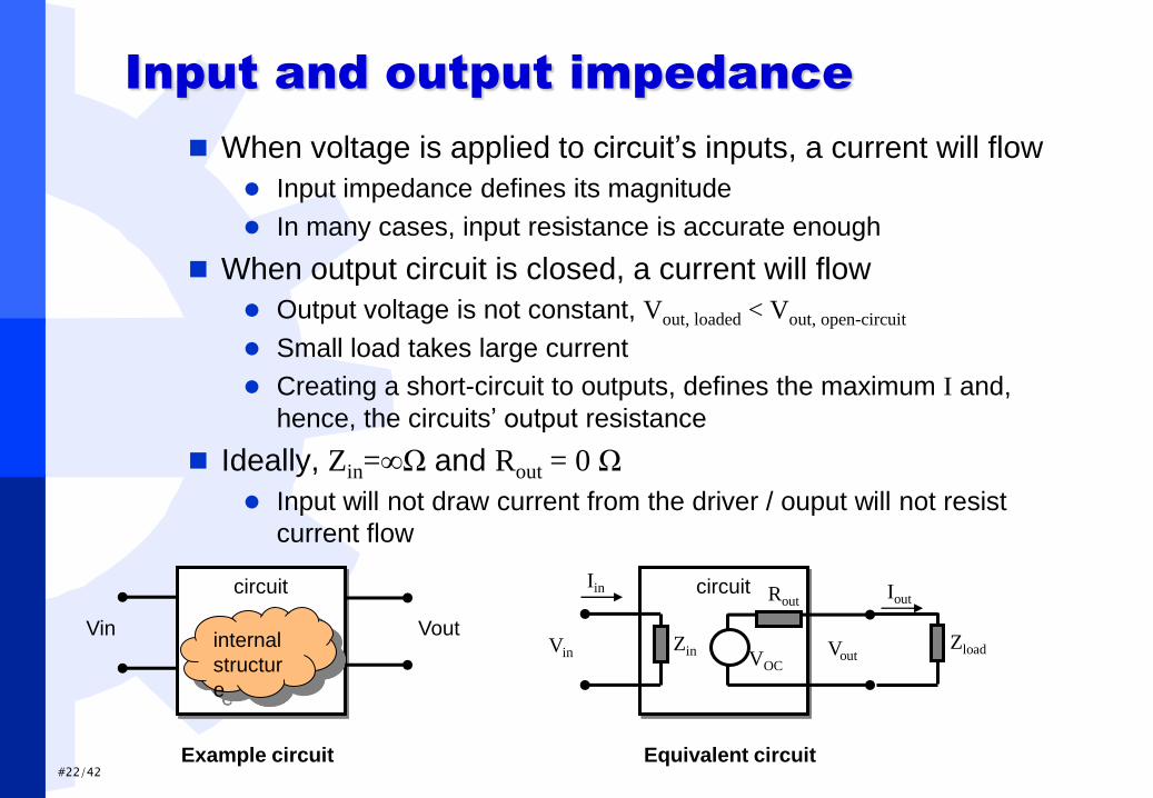
Input and output impedance
When voltage is applied to circuit’s inputs, a current will flow
Input impedance defines its magnitude
In many cases, input resistance is accurate enough
When output circuit is closed, a current will flow
Output voltage is not constant, Vout, loaded < Vout, open-circuit
Small load takes large current
Creating a short-circuit to outputs, defines the maximum I and,
hence, the circuits’ output resistance
Ideally, Zin=∞Ω and Rout = 0 Ω
Input will not draw current from the driver / ouput will not resist
current flow
circuit
internal
structur
e
Vin Vout
circuit
Vin Zin
Rout
Vout
Iin
Example circuit Equivalent circuit
Zload
Iout
VOC
#23/42
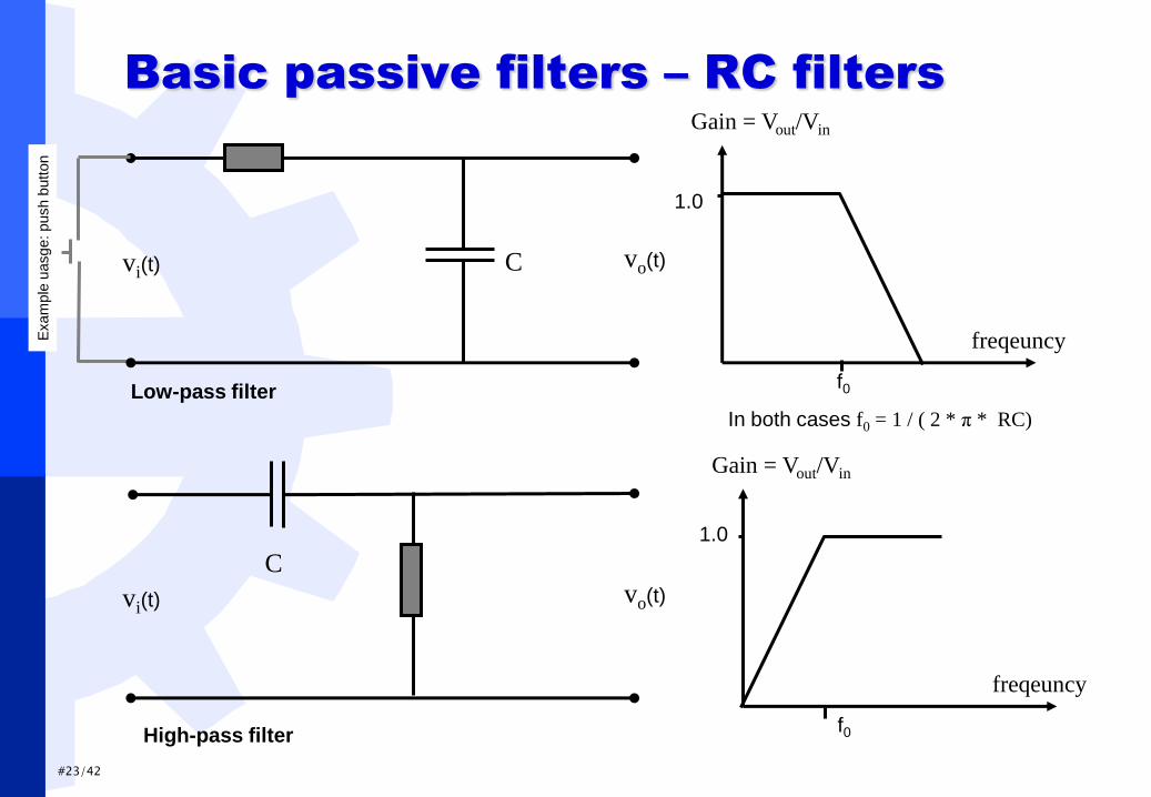
Basic passive filters – RC filters
vo(t)
C
vi(t)
vo(t) C vi(t)
Gain = Vout/Vin
freqeuncy
Gain = Vout/Vin
freqeuncy
1.0
1.0
f0
f0
Low-pass filter
In both cases f0 = 1 / ( 2 * π * RC)
High-pass filter
Exam
ple
uasge: push b
utton
#24/42
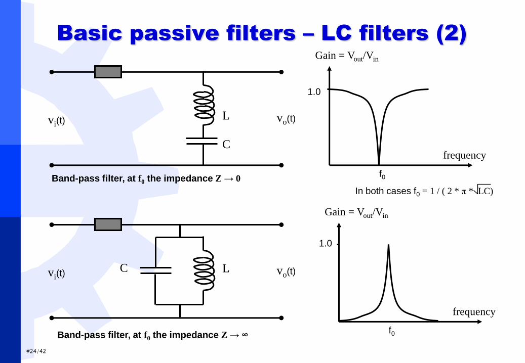
Basic passive filters – LC filters (2)
vo(t) C L vi(t)
vo(t)
C
L vi(t)
Gain = Vout/Vin
frequency
Gain = Vout/Vin
frequency
1.0
1.0
f0
f0
Band-pass filter, at f0 the impedance Z → 0
In both cases f0 = 1 / ( 2 * π * LC)
Band-pass filter, at f0 the impedance Z → ∞
Some semiconductor
devices
#27/42
Semiconductor devices
Semiconductor – material which conducts
varying electrical current depending on the
conditions, e.g. voltage or light
Diode
simplest semiconductor device, two terminals
conducts in one direction
Transistor
three-terminal devices
conductivity is controlled with one of the terminals
Integrated circuits
#28/42
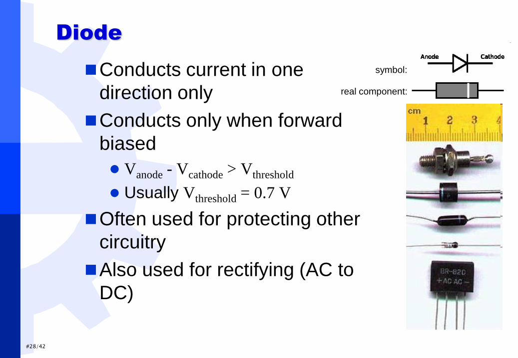
Diode
Conducts current in one
direction only
Conducts only when forward
biased
Vanode - Vcathode > Vthreshold
Usually Vthreshold = 0.7 V
Often used for protecting other
circuitry
Also used for rectifying (AC to
DC)
symbol:
real component:
#29/42
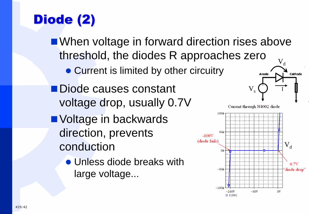
Diode (2)
When voltage in forward direction rises above
threshold, the diodes R approaches zero
Current is limited by other circuitry
Diode causes constant
voltage drop, usually 0.7V
Voltage in backwards
direction, prevents
conduction
Unless diode breaks with
large voltage...
+
- Vs
Vd
Vd
I
#30/42
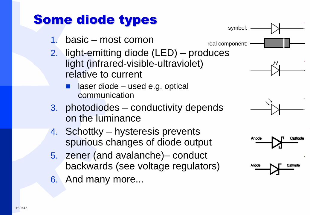
Some diode types
1. basic – most comon
2. light-emitting diode (LED) – produces light (infrared-visible-ultraviolet) relative to current laser diode – used e.g. optical
communication
3. photodiodes – conductivity depends on the luminance
4. Schottky – hysteresis prevents spurious changes of diode output
5. zener (and avalanche)– conduct backwards (see voltage regulators)
6. And many more...
symbol:
real component:
#31/42
#32/42
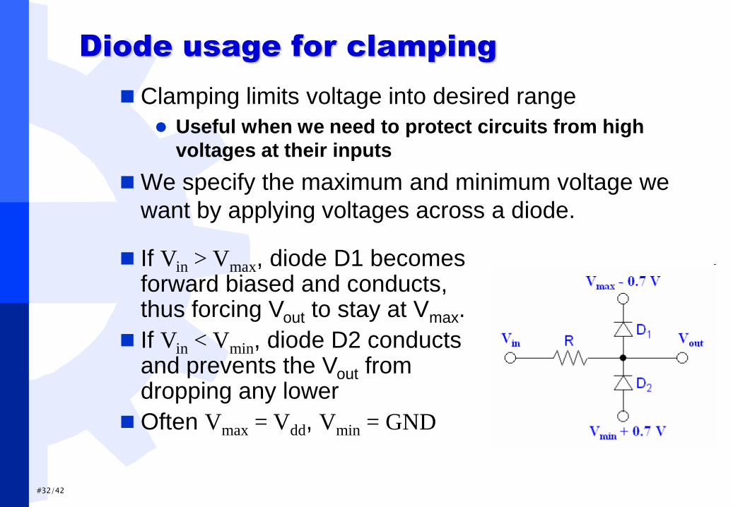
Diode usage for clamping
Clamping limits voltage into desired range
Useful when we need to protect circuits from high
voltages at their inputs
We specify the maximum and minimum voltage we
want by applying voltages across a diode.
If Vin > Vmax, diode D1 becomes forward biased and conducts, thus forcing Vout to stay at Vmax.
If Vin < Vmin, diode D2 conducts and prevents the Vout from dropping any lower
Often Vmax = Vdd, Vmin = GND
#33/42
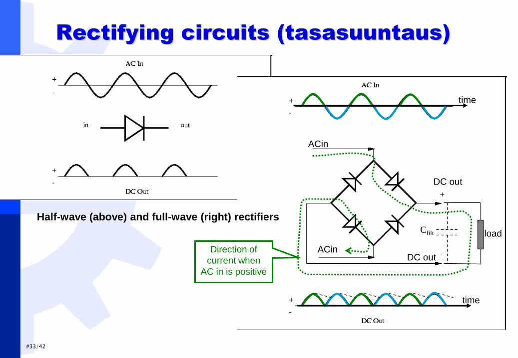
Rectifying circuits (tasasuuntaus)
ACin
ACin
DC out
DC out
time
time
Direction of
current when
AC in is positive
Half-wave (above) and full-wave (right) rectifiers
load Cfilt
#34/42
Transistor
Amplifies or switches electronic signals
Sometimes considered as ”the greatest
invention of 20th century”
Three terminals
current in
current out
control terminal
The last defines the conductivity between the
two others
#35/42
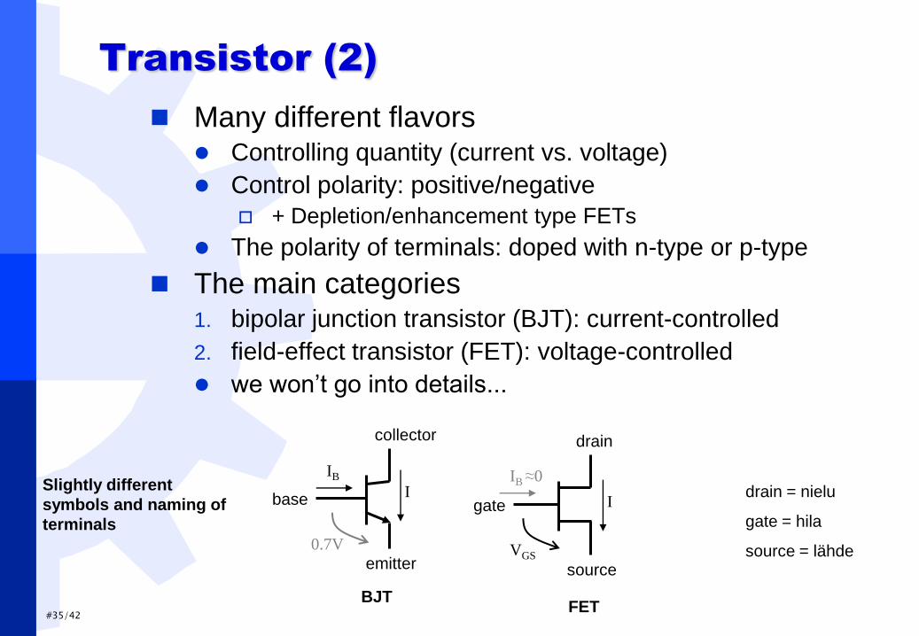
Transistor (2)
Many different flavors Controlling quantity (current vs. voltage)
Control polarity: positive/negative
+ Depletion/enhancement type FETs
The polarity of terminals: doped with n-type or p-type
The main categories 1. bipolar junction transistor (BJT): current-controlled
2. field-effect transistor (FET): voltage-controlled
we won’t go into details...
gate
drain
source
base
collector
emitter
Slightly different
symbols and naming of
terminals
VGS
BJT FET
IB
I I
drain = nielu
gate = hila
source = lähde
IB ≈0
0.7V
#36/42
Transistor (3)
a) Transistor off – not conducting – when
control voltage (or current) is zero
b) Transistor on – starts conducting – when
control voltage increases
1. Conductivity increases with control
2. When control increases enough, transistor
becomes saturated – it cannot conduct more
current
When conducting, base-emitter voltage (or
gate-source) is constant
Similar p-n junction as in diode
#39/42
Example usages of
transistor
1. As a switch
FET closes the electrical circuit and let’s the current flow
Practically zero current goes from PIC to FET
Specific power-FETs can handle large currents
2. As inverting AC amplifier
This BJT has DC current gain hFE = β = 100
IB = (Vcc- 0.7V)/RB = 10.2 uA
IC = β * IB = 1.02 mA
quiescent Vo = Vcc – IC * RC = 5.2V
Vin > 0, increases IB and Vout will drop
With few additional R, the gain can be controlled regardless of β
g
d
s VGS
I
Device that takes
larger current than
available from PIC
Vdd
PIC
GPIO
IB
IC
0.7V
Vin
Vcc = 10V
Rb= 910 kΩ
b
c
e Vout
Rc= 4.7 kΩ
0V
C
#40/42
Integrated circuits
An integrated circuit (IC) combines many
components into single chip
Example ICs
microprocessor
memory
Ethernet controller
operational amplifier
74xx series, e.g. 8 * 2AND gates
Require larger package with more pins than
previously introduced components
Using ICs reduces the number of components on the
circuit board and increase their performance
#41/42
Operational amplifier
High-gain voltage amplifier
Very popular active component
Needs power supply and ground
Amplifies the difference between the two
input terminals An op-amp in a DIP
package
+
-
Vs+
Vs-
V+
V-.
Vout.
For any input voltages the ideal op-amp has infinite open-loop gain (i.e.
without feedback)
infinite bandwidth and slew rate
infinite input impedances (resulting in zero input currents),
zero offset voltage,output impedance, and noise
Circuit symbol of an op. amp.
#42/42
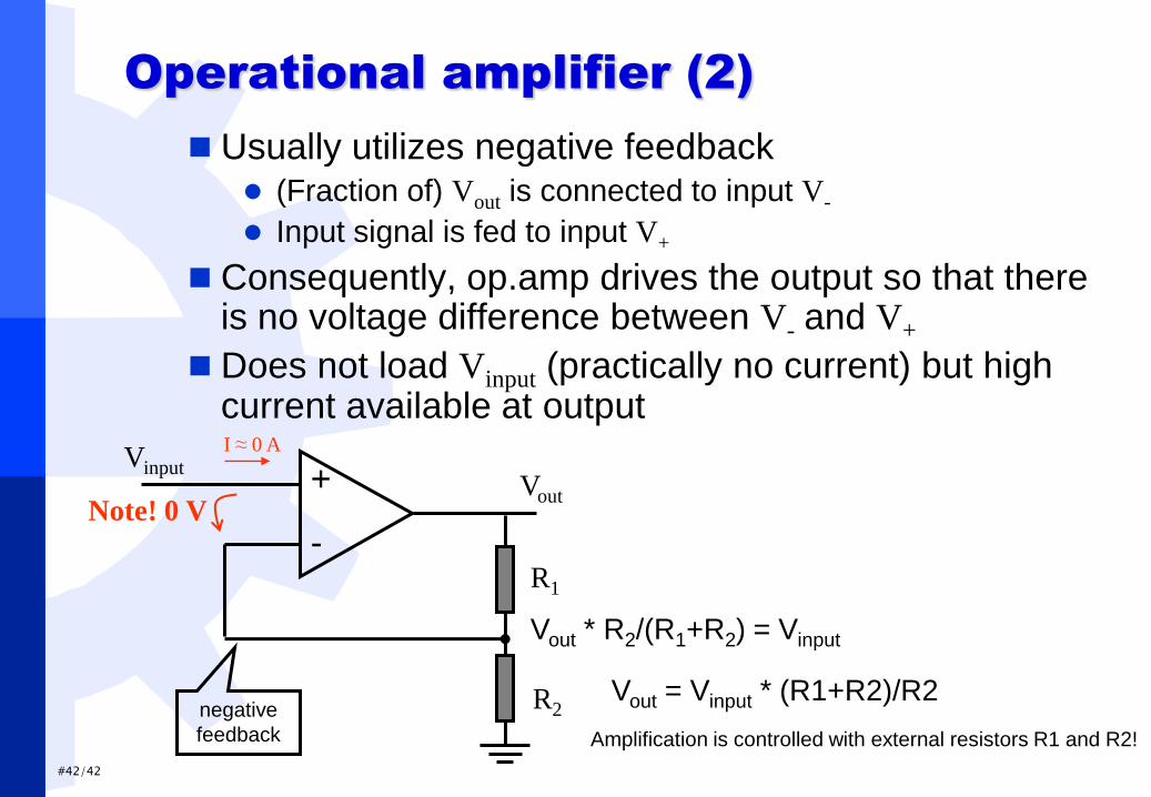
Operational amplifier (2)
Usually utilizes negative feedback (Fraction of) Vout is connected to input V-
Input signal is fed to input V+
Consequently, op.amp drives the output so that there is no voltage difference between V- and V+
Does not load Vinput (practically no current) but high current available at output
+
- R1
R2
Vinput Vout
Vout * R2/(R1+R2) = Vinput
Note! 0 V
Vout = Vinput * (R1+R2)/R2 negative
feedback
I ≈ 0 A
Amplification is controlled with external resistors R1 and R2!
Mikko Kohvakka - Nov 2009
TKT-3500
Microcontroller
systems
Lec 6 – PCB design
Mikko Kohvakka
Department of Computer Systems
Tampere University of Technology
Fall 2009
#44/42
Following slides
Originally presented and made by Mikko
Kohvakka
He has designed most of the TUTWSN main
boards, including the one used in practices
PhD in area of Wireless Sensor Network PHY
and MAC
#45/42 Mikko Kohvakka - Nov 2009
Contents
Electronic components
Printed Circuit Board (PCB) Design 1. schematic design
2. placement
3. routing
4. verification
5. manufacturing
6. testing
Example schedule and prices
Electromagentic Compatibility (EMC) issues Emission types: radiated adn conducted
Electrostatic discharge (ESD)
Mikko Kohvakka - Nov 2009
Electronic components
#47/42 Mikko Kohvakka - Nov 2009
Real-life components
All real component have parasitics R, C and L Also the wires!
In many cases, these parasitics can be neglected, for example, at low frequencies
Real-life components are not 100% accurate e.g. a nominally 100 Ω resistor may actually be
90 Ω or 110 Ω, or something in between
Components come with x% tolerance e.g. 1%, 5%, 10% tolerance
Smaller the tolerance, the more expensive
Very HIFI devices may use manually picked components
#48/42 Mikko Kohvakka - Nov 2009
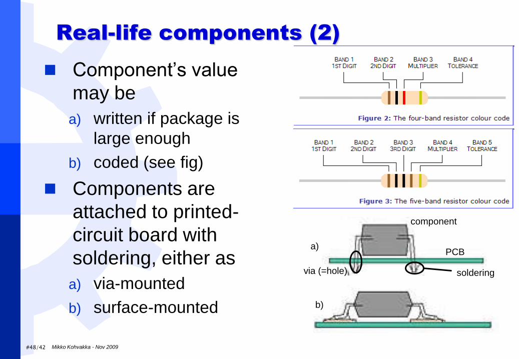
Real-life components (2)
Component’s value
may be
a) written if package is
large enough
b) coded (see fig)
Components are
attached to printed-
circuit board with
soldering, either as
a) via-mounted
b) surface-mounted
a)
b)
PCB
soldering via (=hole)
component
#49/42 Mikko Kohvakka - Nov 2009
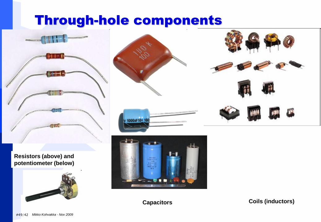
Through-hole components
Resistors (above) and
potentiometer (below)
Capacitors Coils (inductors)
#50/42 Mikko Kohvakka - Nov 2009
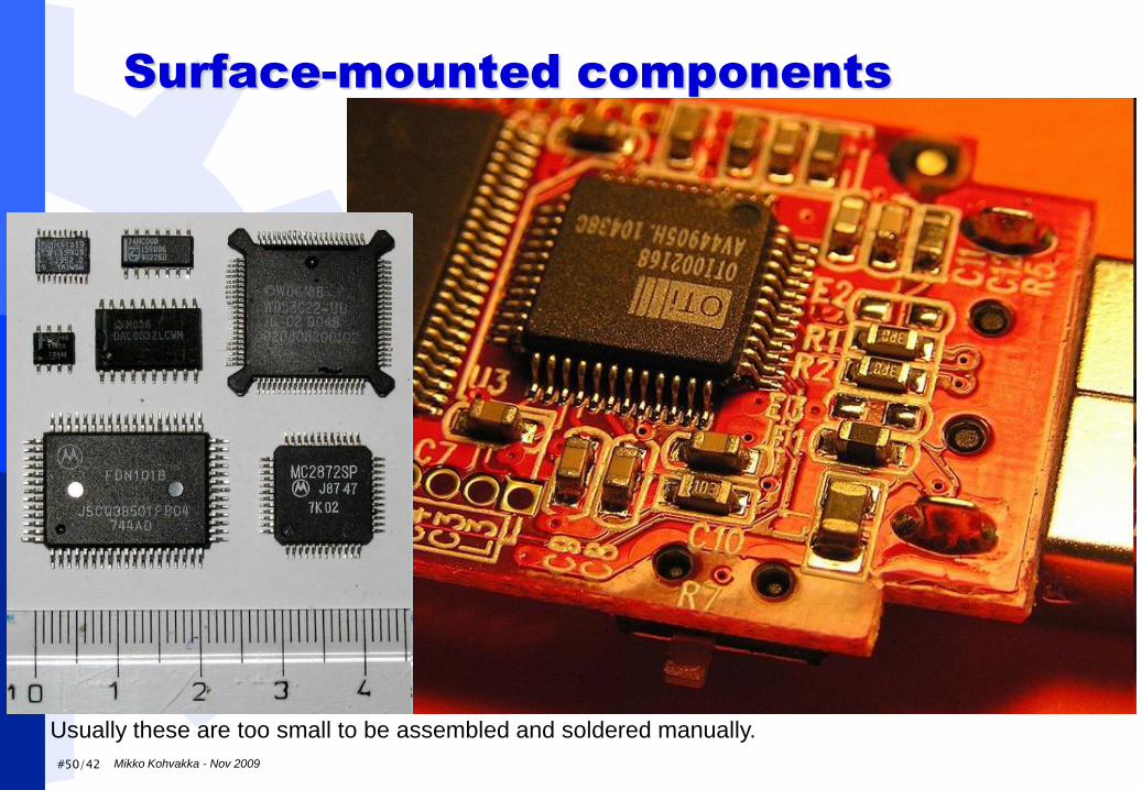
Surface-mounted components
Usually these are too small to be assembled and soldered manually.
#51/42 Mikko Kohvakka - Nov 2009
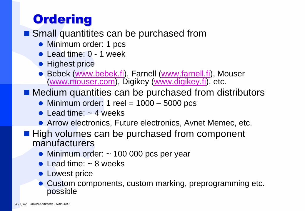
Ordering
Small quantitites can be purchased from Minimum order: 1 pcs
Lead time: 0 - 1 week
Highest price
Bebek (www.bebek.fi), Farnell (www.farnell.fi), Mouser (www.mouser.com), Digikey (www.digikey.fi), etc.
Medium quantities can be purchased from distributors Minimum order: 1 reel = 1000 – 5000 pcs
Lead time: ~ 4 weeks
Arrow electronics, Future electronics, Avnet Memec, etc.
High volumes can be purchased from component manufacturers Minimum order: ~ 100 000 pcs per year
Lead time: ~ 8 weeks
Lowest price
Custom components, custom marking, preprogramming etc. possible
Mikko Kohvakka - Nov 2009
Printed Circuit Board
(PCB) Design
#53/42 Mikko Kohvakka - Nov 2009
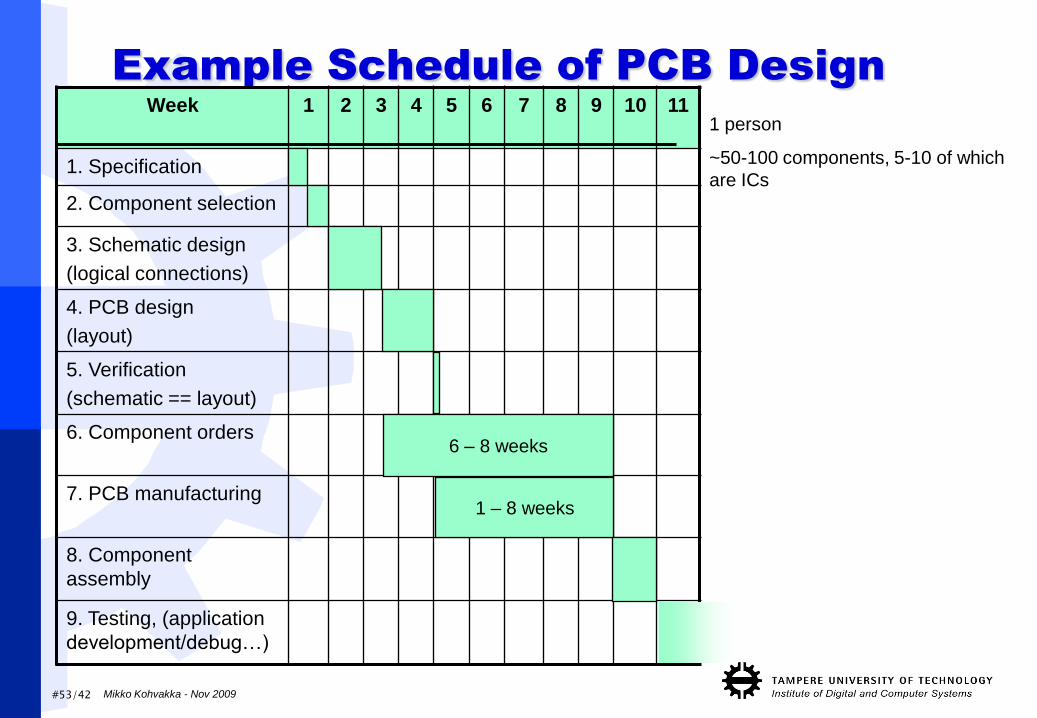
Example Schedule of PCB Design
Week 1 2 3 4 5 6 7 8 9 10 11
1. Specification
2. Component selection
3. Schematic design
(logical connections)
4. PCB design
(layout)
5. Verification
(schematic == layout)
6. Component orders
7. PCB manufacturing
8. Component
assembly
9. Testing, (application
development/debug…)
6 – 8 weeks
1 – 8 weeks
1 person
~50-100 components, 5-10 of which
are ICs
#54/42 Mikko Kohvakka - Nov 2009
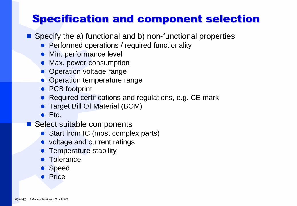
Specification and component selection
Specify the a) functional and b) non-functional properties Performed operations / required functionality
Min. performance level
Max. power consumption
Operation voltage range
Operation temperature range
PCB footprint
Required certifications and regulations, e.g. CE mark
Target Bill Of Material (BOM)
Etc.
Select suitable components Start from IC (most complex parts)
voltage and current ratings
Temperature stability
Tolerance
Speed
Price
#55/42 Mikko Kohvakka - Nov 2009
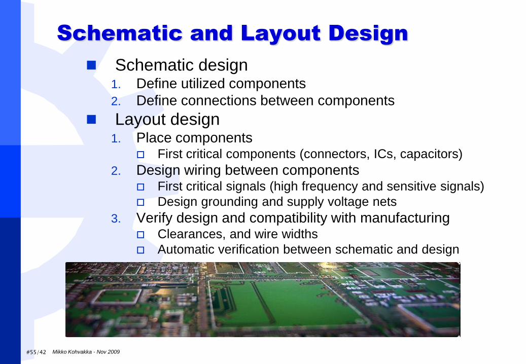
Schematic and Layout Design
Schematic design 1. Define utilized components
2. Define connections between components
Layout design 1. Place components
First critical components (connectors, ICs, capacitors)
2. Design wiring between components First critical signals (high frequency and sensitive signals)
Design grounding and supply voltage nets
3. Verify design and compatibility with manufacturing Clearances, and wire widths
Automatic verification between schematic and design
#56/42 Mikko Kohvakka - Nov 2009
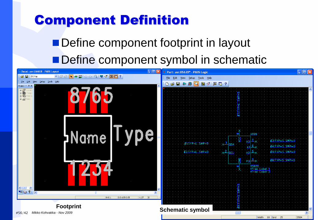
Component Definition
Define component footprint in layout
Define component symbol in schematic
Footprint Schematic symbol
#57/42 Mikko Kohvakka - Nov 2009
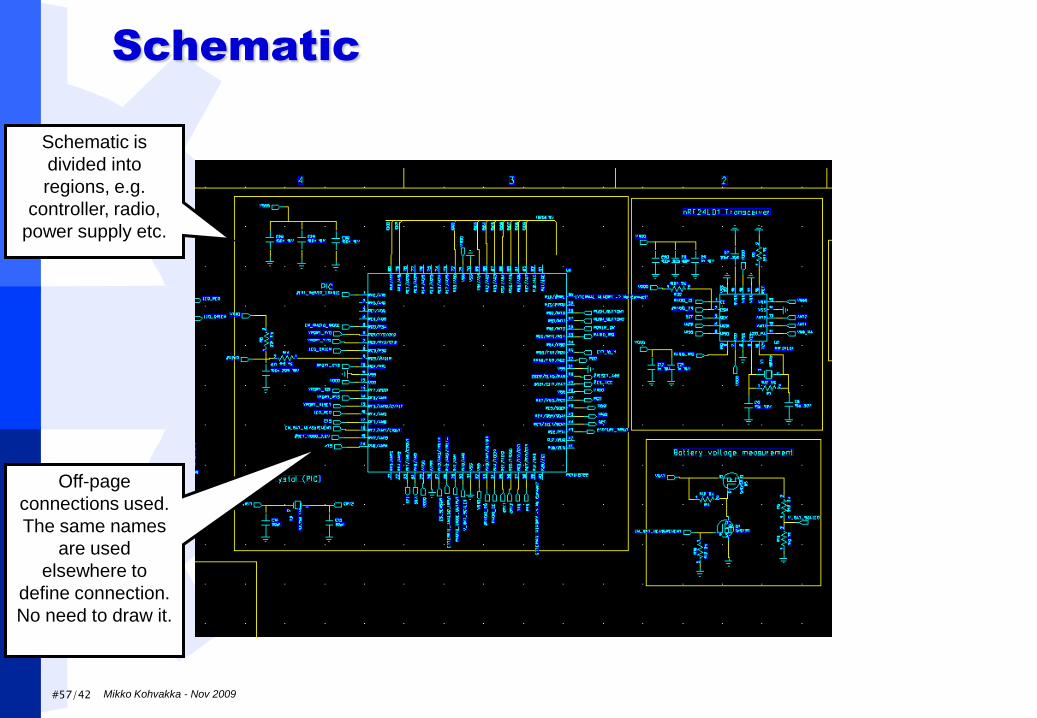
Schematic
Schematic is
divided into
regions, e.g.
controller, radio,
power supply etc.
Off-page
connections used.
The same names
are used
elsewhere to
define connection.
No need to draw it.
#58/42 Mikko Kohvakka - Nov 2009
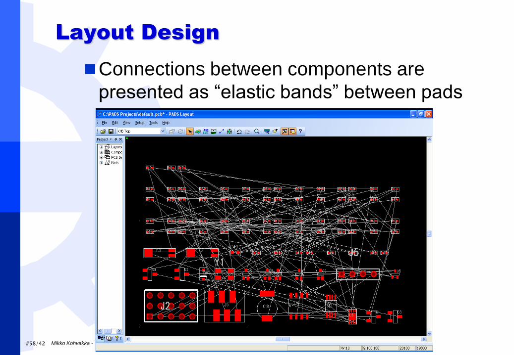
Layout Design
Connections between components are
presented as “elastic bands” between pads
#59/42 Mikko Kohvakka - Nov 2009
Component Placement
Use the link between schematic and PCB
A components are selected in schematic they become
selected in layout too
Divide components in blocks, e.g. regulator block,
MCU block, sensor block etc.
Easy by using the link and selecting the block in schematic
Design layout first for blocks, then place the blocks in
the design in correct places
Critical components first, e.g. ICs and crystals
Critical signals first (clk, analog)
Capacitors near to ICs
Try to minimize routing lengths
#60/42 Mikko Kohvakka - Nov 2009
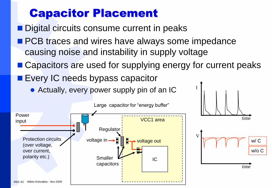
Capacitor Placement
Digital circuits consume current in peaks
PCB traces and wires have always some impedance
causing noise and instability in supply voltage
Capacitors are used for supplying energy for current peaks
Every IC needs bypass capacitor
Actually, every power supply pin of an IC
Power
input
Protection circuits
(over voltage,
over current,
polarity etc.)
Large capacitor for “energy buffer”
IC
VCC1 area
Regulator
Smaller
capacitors
voltage in voltage out
time
I
time
V
w/o C
w/ C
#61/42 Mikko Kohvakka - Nov 2009
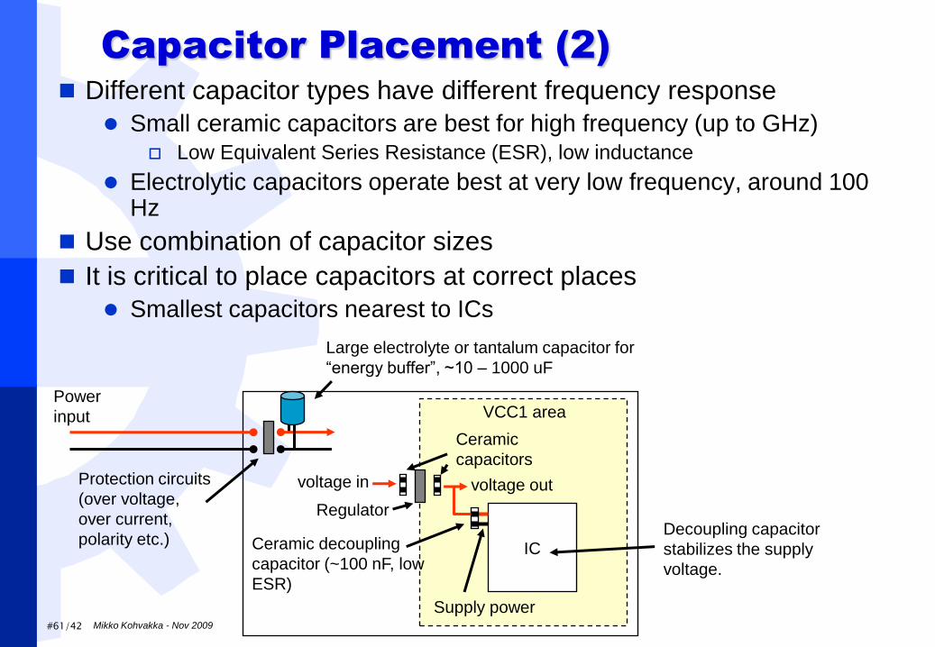
Capacitor Placement (2)
Different capacitor types have different frequency response
Small ceramic capacitors are best for high frequency (up to GHz) Low Equivalent Series Resistance (ESR), low inductance
Electrolytic capacitors operate best at very low frequency, around 100 Hz
Use combination of capacitor sizes
It is critical to place capacitors at correct places
Smallest capacitors nearest to ICs
Power
input
Protection circuits
(over voltage,
over current,
polarity etc.)
Large electrolyte or tantalum capacitor for
“energy buffer”, ~10 – 1000 uF
IC
Supply power
Ceramic decoupling
capacitor (~100 nF, low
ESR)
VCC1 area
Regulator
Ceramic
capacitors
Decoupling capacitor
stabilizes the supply
voltage.
voltage in voltage out
#62/42 Mikko Kohvakka - Nov 2009
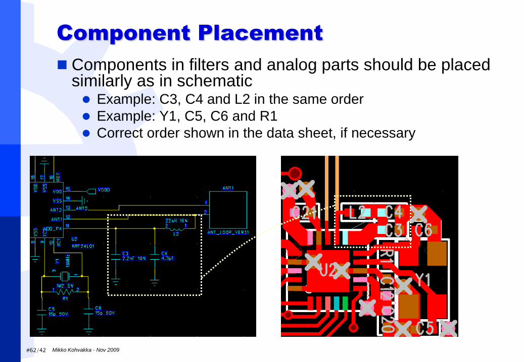
Component Placement
Components in filters and analog parts should be placed similarly as in schematic Example: C3, C4 and L2 in the same order
Example: Y1, C5, C6 and R1
Correct order shown in the data sheet, if necessary
#63/42 Mikko Kohvakka - Nov 2009
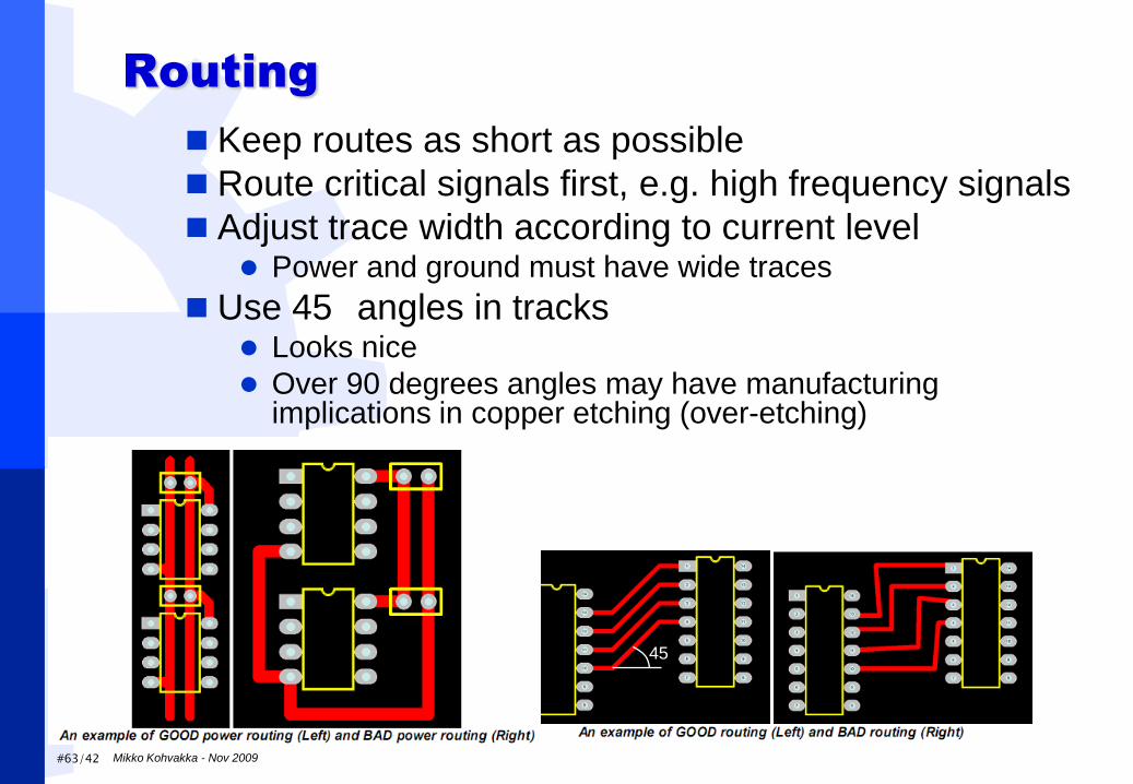
Routing
Keep routes as short as possible
Route critical signals first, e.g. high frequency signals
Adjust trace width according to current level Power and ground must have wide traces
Use 45 angles in tracks Looks nice
Over 90 degrees angles may have manufacturing implications in copper etching (over-etching)
45
#64/42 Mikko Kohvakka - Nov 2009
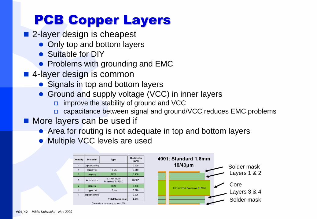
PCB Copper Layers
2-layer design is cheapest Only top and bottom layers
Suitable for DIY
Problems with grounding and EMC
4-layer design is common Signals in top and bottom layers
Ground and supply voltage (VCC) in inner layers improve the stability of ground and VCC
capacitance between signal and ground/VCC reduces EMC problems
More layers can be used if Area for routing is not adequate in top and bottom layers
Multiple VCC levels are used
Layers 1 & 2
Layers 3 & 4
Core
Solder mask
Solder mask
#65/42 Mikko Kohvakka - Nov 2009
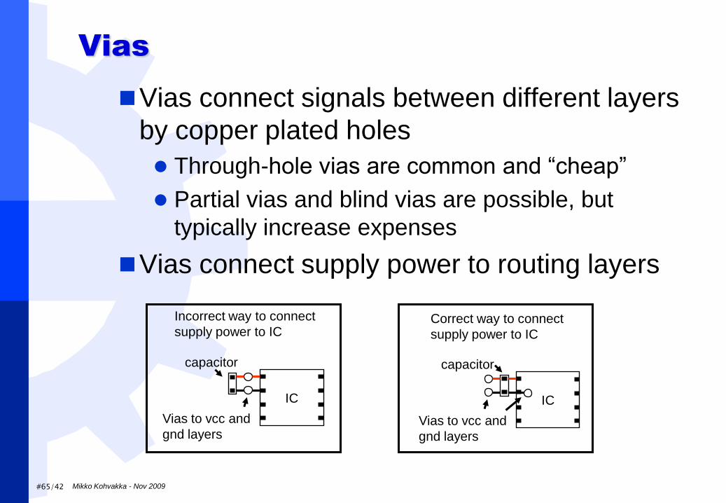
Vias
Vias connect signals between different layers
by copper plated holes
Through-hole vias are common and “cheap”
Partial vias and blind vias are possible, but
typically increase expenses
Vias connect supply power to routing layers
IC
capacitor
Vias to vcc and
gnd layers
Incorrect way to connect
supply power to IC
IC
capacitor
Vias to vcc and
gnd layers
Correct way to connect
supply power to IC
#66/42 Mikko Kohvakka - Nov 2009
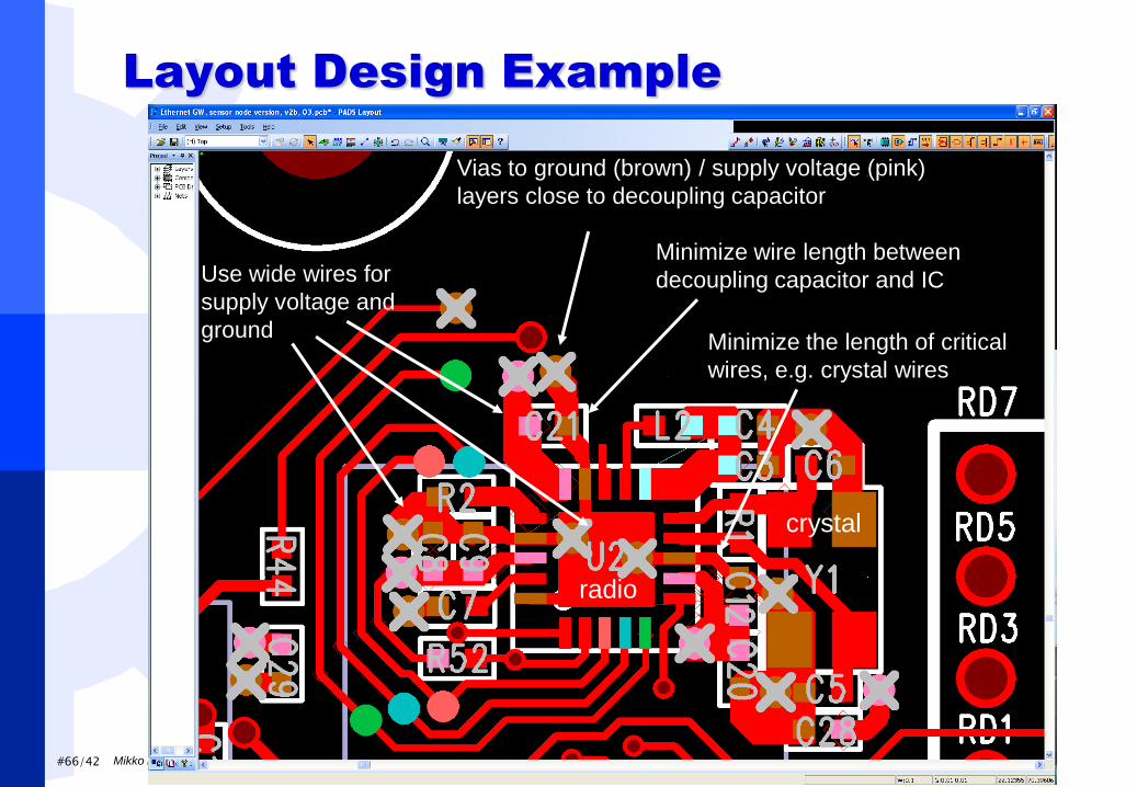
Layout Design Example
Minimize wire length between
decoupling capacitor and IC Use wide wires for
supply voltage and
ground Minimize the length of critical
wires, e.g. crystal wires
Vias to ground (brown) / supply voltage (pink)
layers close to decoupling capacitor
crystal
radio

#67/42 Mikko Kohvakka - Nov 2009
Layout (4–layer design example)
1st layer (routing) 2nd layer (supply voltage) 3rd layer (ground) 4th layer (routing)
Cut prevents
heat flow into
temperature
sensor
#68/42 Mikko Kohvakka - Nov 2009
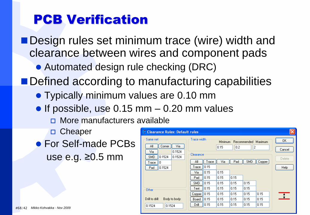
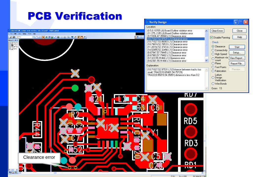
PCB Verification
Design rules set minimum trace (wire) width and clearance between wires and component pads Automated design rule checking (DRC)
Defined according to manufacturing capabilities Typically minimum values are 0.10 mm
If possible, use 0.15 mm – 0.20 mm values More manufacturers available
Cheaper
For Self-made PCBs
use e.g. ≥0.5 mm
#69/42 Mikko Kohvakka - Nov 2009
PCB Verification
Clearance error
#70/42 Mikko Kohvakka - Nov 2009
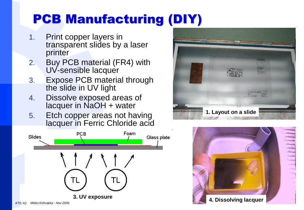
PCB Manufacturing (DIY)
1. Print copper layers in transparent slides by a laser printer
2. Buy PCB material (FR4) with UV-sensible lacquer
3. Expose PCB material through the slide in UV light
4. Dissolve exposed areas of lacquer in NaOH + water
5. Etch copper areas not having lacquer in Ferric Chloride acid
1. Layout on a slide
4. Dissolving lacquer 3. UV exposure
#71/42 Mikko Kohvakka - Nov 2009
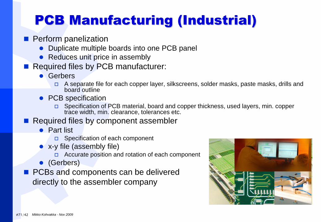
PCB Manufacturing (Industrial)
Perform panelization Duplicate multiple boards into one PCB panel
Reduces unit price in assembly
Required files by PCB manufacturer: Gerbers
A separate file for each copper layer, silkscreens, solder masks, paste masks, drills and board outline
PCB specification Specification of PCB material, board and copper thickness, used layers, min. copper
trace width, min. clearance, tolerances etc.
Required files by component assembler Part list
Specification of each component
x-y file (assembly file) Accurate position and rotation of each component
(Gerbers)
PCBs and components can be delivered
directly to the assembler company
#72/42 Mikko Kohvakka - Nov 2009
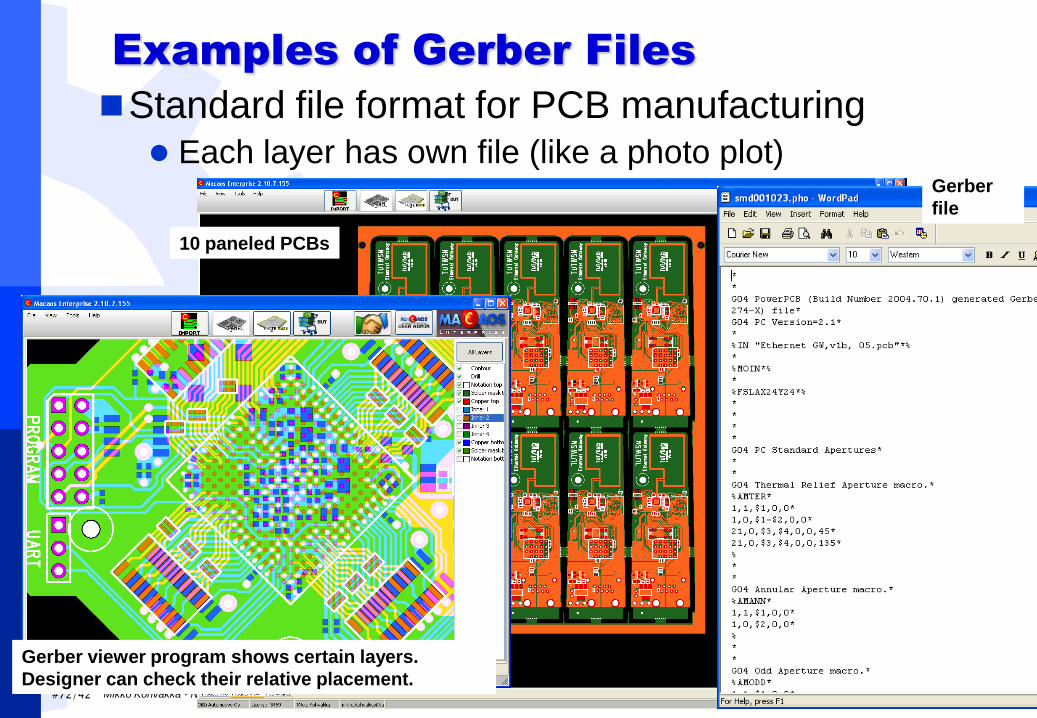
Examples of Gerber Files
Standard file format for PCB manufacturing Each layer has own file (like a photo plot)
10 paneled PCBs
Gerber viewer program shows certain layers.
Designer can check their relative placement.
Gerber
file
#73/42 Mikko Kohvakka - Nov 2009
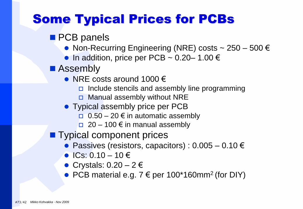
Some Typical Prices for PCBs
PCB panels Non-Recurring Engineering (NRE) costs ~ 250 – 500 €
In addition, price per PCB ~ 0.20– 1.00 €
Assembly NRE costs around 1000 €
Include stencils and assembly line programming
Manual assembly without NRE
Typical assembly price per PCB 0.50 – 20 € in automatic assembly
20 – 100 € in manual assembly
Typical component prices Passives (resistors, capacitors) : 0.005 – 0.10 €
ICs: 0.10 – 10 €
Crystals: 0.20 – 2 €
PCB material e.g. 7 € per 100*160mm2 (for DIY)
#74/42 Mikko Kohvakka - Nov 2009
PCB Price Optimization
Compare component prices and lead times
Minimize the number of different components Reduces assembly and component costs
Define the needed tolerances Do not select 1% resistors, if 5% is adequate
Use only SMD components surface-mounted devices are cheaper to assemble
Minimize board area (and needed wiring layers) Reduces PCB cost
Define the needed PCB manufacturing accuracy Higher clearance, trace width reduces PCB cost
If possible, use only one side of PCB for components Reduces assembly cost
#75/42 Mikko Kohvakka - Nov 2009
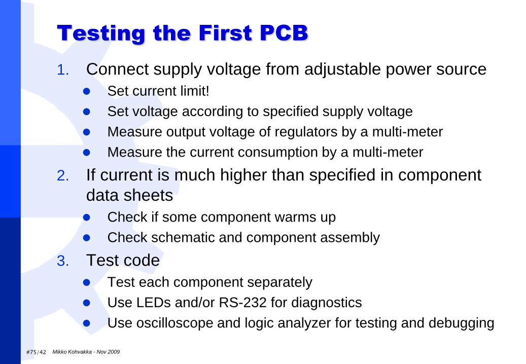
Testing the First PCB
1. Connect supply voltage from adjustable power source
Set current limit!
Set voltage according to specified supply voltage
Measure output voltage of regulators by a multi-meter
Measure the current consumption by a multi-meter
2. If current is much higher than specified in component
data sheets
Check if some component warms up
Check schematic and component assembly
3. Test code
Test each component separately
Use LEDs and/or RS-232 for diagnostics
Use oscilloscope and logic analyzer for testing and debugging
Mikko Kohvakka - Nov 2009
EMC Issues
#77/42 Mikko Kohvakka - Nov 2009
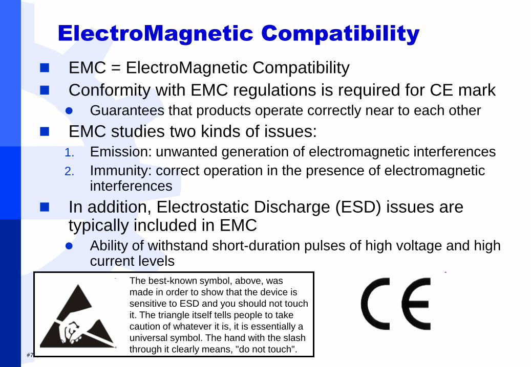
ElectroMagnetic Compatibility
EMC = ElectroMagnetic Compatibility
Conformity with EMC regulations is required for CE mark Guarantees that products operate correctly near to each other
EMC studies two kinds of issues: 1. Emission: unwanted generation of electromagnetic interferences
2. Immunity: correct operation in the presence of electromagnetic interferences
In addition, Electrostatic Discharge (ESD) issues are typically included in EMC Ability of withstand short-duration pulses of high voltage and high
current levels
The best-known symbol, above, was
made in order to show that the device is
sensitive to ESD and you should not touch
it. The triangle itself tells people to take
caution of whatever it is, it is essentially a
universal symbol. The hand with the slash
through it clearly means, "do not touch".
#78/42 Mikko Kohvakka - Nov 2009
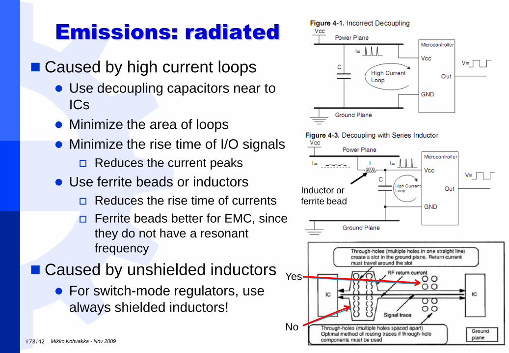
Emissions: radiated
Caused by high current loops
Use decoupling capacitors near to
ICs
Minimize the area of loops
Minimize the rise time of I/O signals
Reduces the current peaks
Use ferrite beads or inductors
Reduces the rise time of currents
Ferrite beads better for EMC, since
they do not have a resonant
frequency
Caused by unshielded inductors
For switch-mode regulators, use
always shielded inductors!
Inductor or
ferrite bead
Yes
No
#79/42 Mikko Kohvakka - Nov 2009
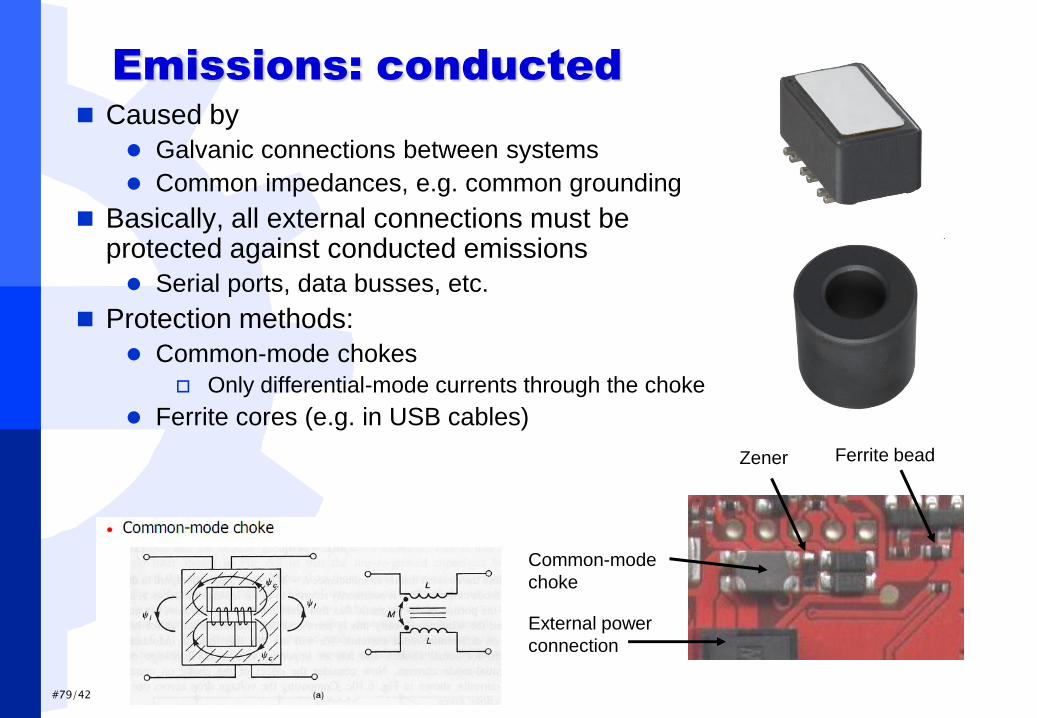
Emissions: conducted
Caused by
Galvanic connections between systems
Common impedances, e.g. common grounding
Basically, all external connections must be protected against conducted emissions
Serial ports, data busses, etc.
Protection methods:
Common-mode chokes
Only differential-mode currents through the choke
Ferrite cores (e.g. in USB cables)
Common-mode
choke
External power
connection
Ferrite bead Zener
#80/42 Mikko Kohvakka - Nov 2009
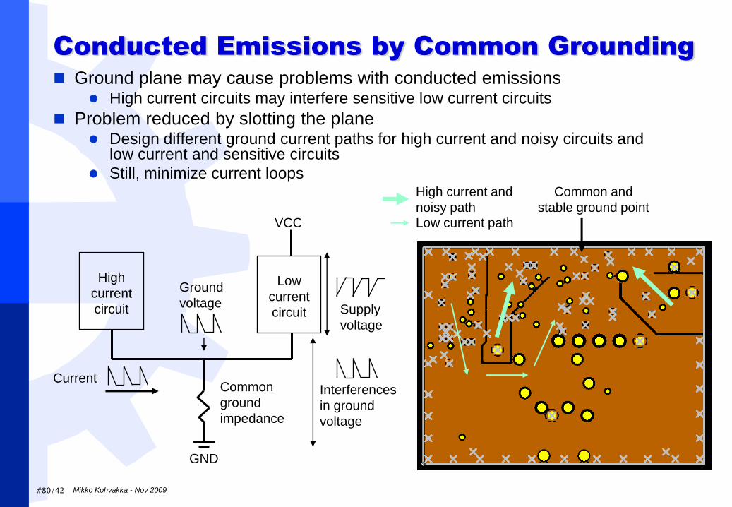
Conducted Emissions by Common Grounding
Ground plane may cause problems with conducted emissions High current circuits may interfere sensitive low current circuits
Problem reduced by slotting the plane Design different ground current paths for high current and noisy circuits and
low current and sensitive circuits
Still, minimize current loops
High
current
circuit
Low
current
circuit
GND
Common
ground
impedance
Current
Ground
voltage
Interferences
in ground
voltage
High current and
noisy path
Common and
stable ground point Low current path
Supply
voltage
VCC

#81/42 Mikko Kohvakka - Nov 2009
Immunity for Interferences
A product must be able to operate correctly in the presence of electromagnetic field E.g. near a mobile phone or microwave oven
The design guidelines for eliminating emissions apply also for immunity Loops etc. act as antennas and induce current to the
PCB
Effects are reduced by ground planes Fill unused PCB area with copper connected to
ground
Use ground between critical signals
System packaging prevents radiated emissions Metal cage, minimal holes, safety ground
#82/42 Mikko Kohvakka - Nov 2009
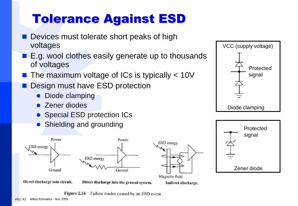
Tolerance Against ESD
Devices must tolerate short peaks of high voltages
E.g. wool clothes easily generate up to thousands of voltages
The maximum voltage of ICs is typically < 10V
Design must have ESD protection
Diode clamping
Zener diodes
Special ESD protection ICs
Shielding and grounding
VCC (supply voltage)
Protected
signal
Protected
signal
Diode clamping
Zener diode
#83/42 Mikko Kohvakka - Nov 2009
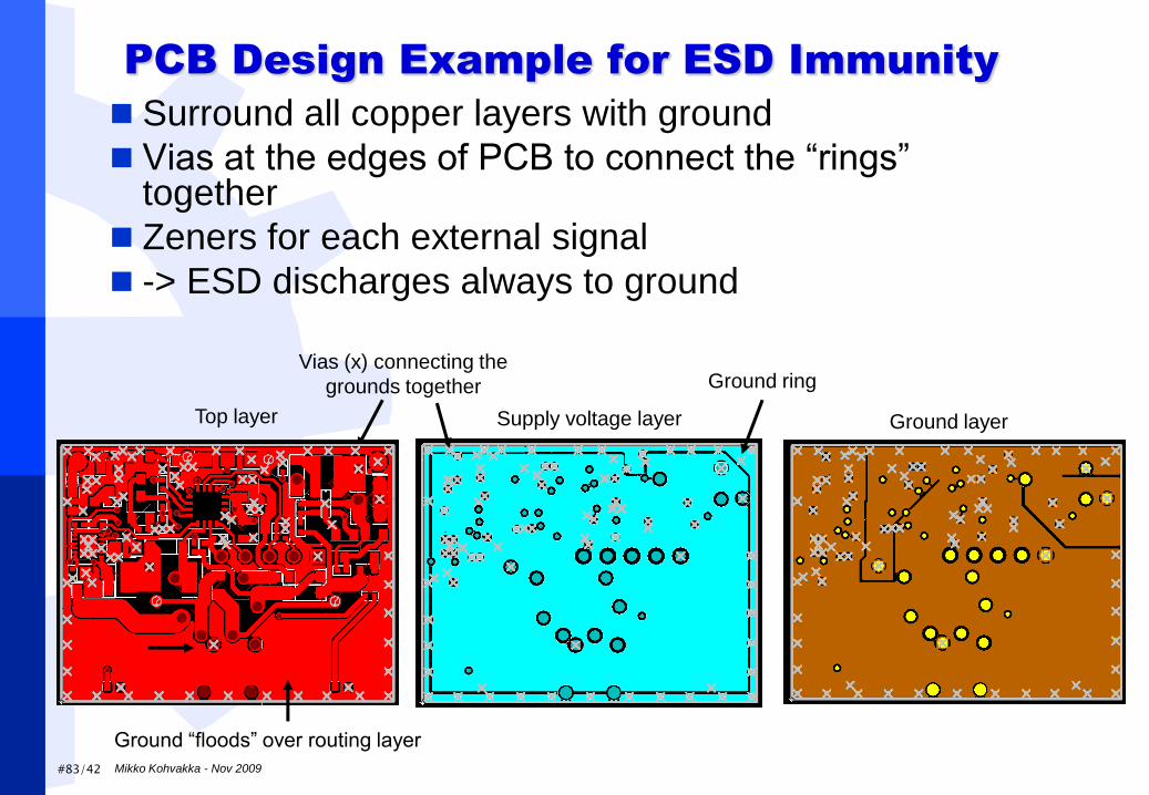
PCB Design Example for ESD Immunity
Surround all copper layers with ground
Vias at the edges of PCB to connect the “rings” together
Zeners for each external signal
-> ESD discharges always to ground
Supply voltage layer Ground layer
Ground ring Vias (x) connecting the
grounds together
Ground “floods” over routing layer
Top layer
#84/42 Mikko Kohvakka - Nov 2009
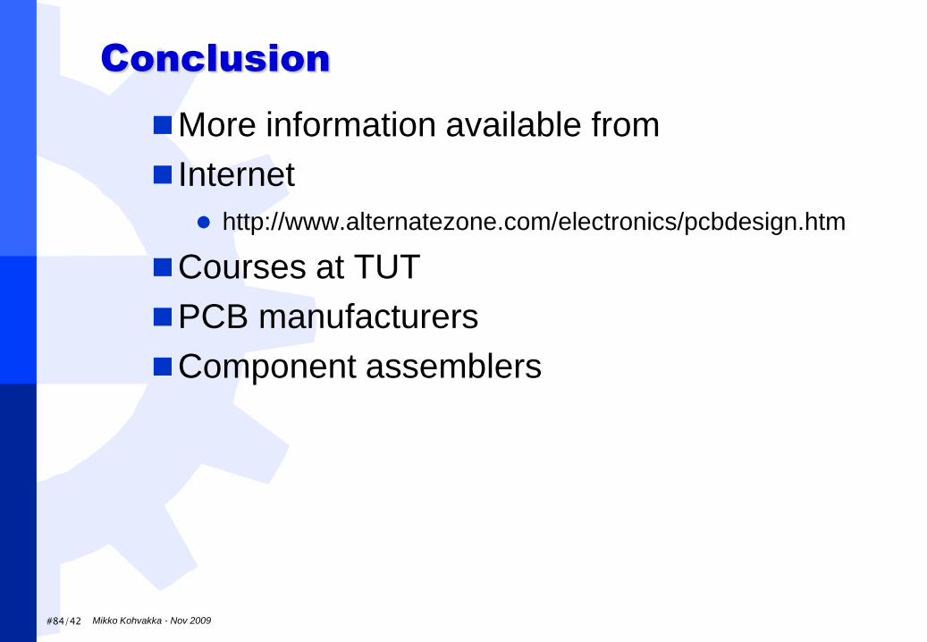
Conclusion
More information available from
Internet
http://www.alternatezone.com/electronics/pcbdesign.htm
Courses at TUT
PCB manufacturers
Component assemblers
#85/42
CONCLUSIVE QUICK GUIDE
TO A HOBBYIST
By Teemu Laukkarinen (this is the core understanding of HW in this
course)
#86/42
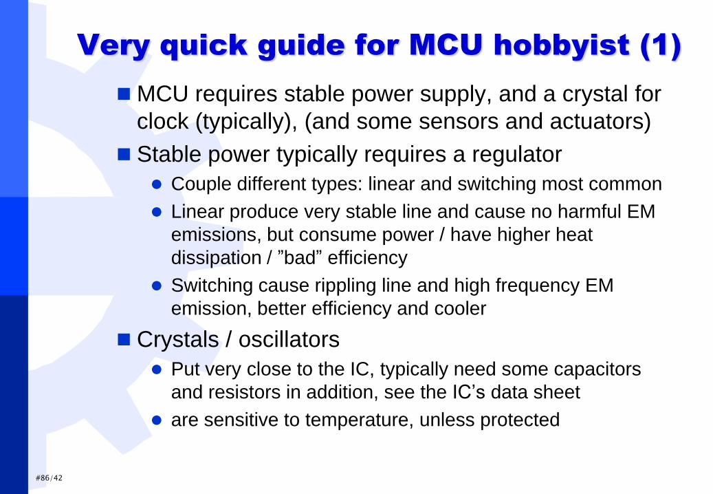
Very quick guide for MCU hobbyist (1)
MCU requires stable power supply, and a crystal for
clock (typically), (and some sensors and actuators)
Stable power typically requires a regulator
Couple different types: linear and switching most common
Linear produce very stable line and cause no harmful EM
emissions, but consume power / have higher heat
dissipation / ”bad” efficiency
Switching cause rippling line and high frequency EM
emission, better efficiency and cooler
Crystals / oscillators
Put very close to the IC, typically need some capacitors
and resistors in addition, see the IC’s data sheet
are sensitive to temperature, unless protected
#87/42
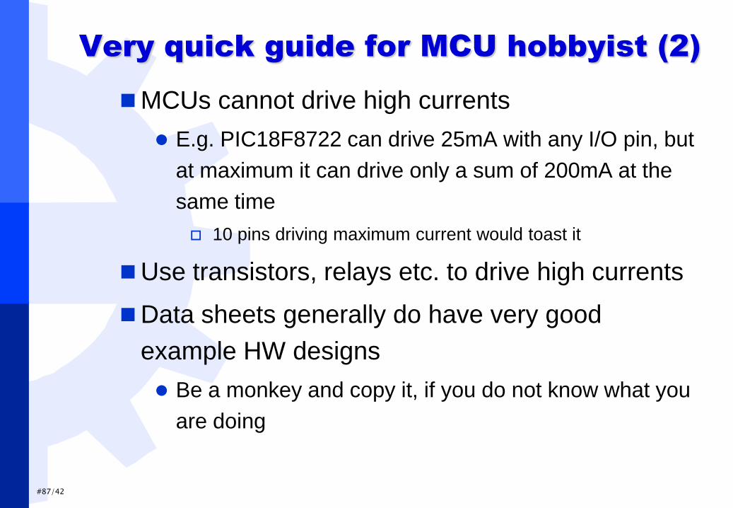
Very quick guide for MCU hobbyist (2)
MCUs cannot drive high currents
E.g. PIC18F8722 can drive 25mA with any I/O pin, but
at maximum it can drive only a sum of 200mA at the
same time
10 pins driving maximum current would toast it
Use transistors, relays etc. to drive high currents
Data sheets generally do have very good
example HW designs
Be a monkey and copy it, if you do not know what you
are doing
#88/42
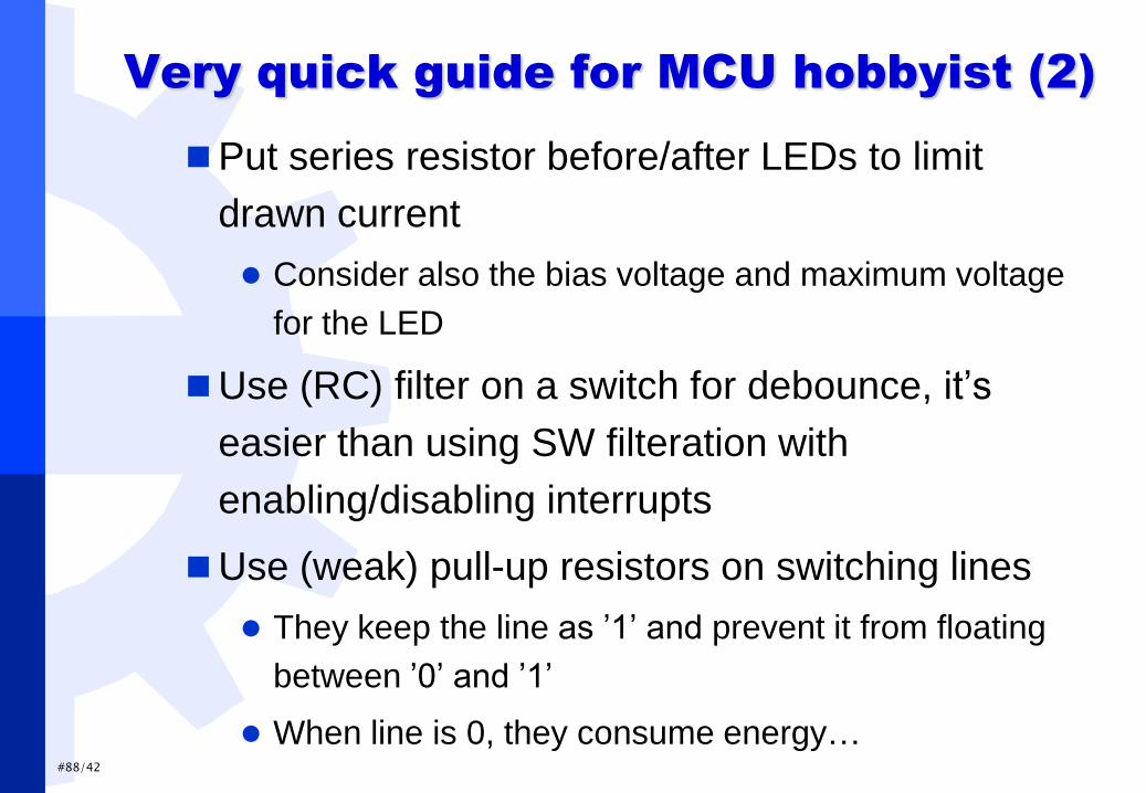
Very quick guide for MCU hobbyist (2)
Put series resistor before/after LEDs to limit
drawn current
Consider also the bias voltage and maximum voltage
for the LED
Use (RC) filter on a switch for debounce, it’s
easier than using SW filteration with
enabling/disabling interrupts
Use (weak) pull-up resistors on switching lines
They keep the line as ’1’ and prevent it from floating
between ’0’ and ’1’
When line is 0, they consume energy…
#89/42
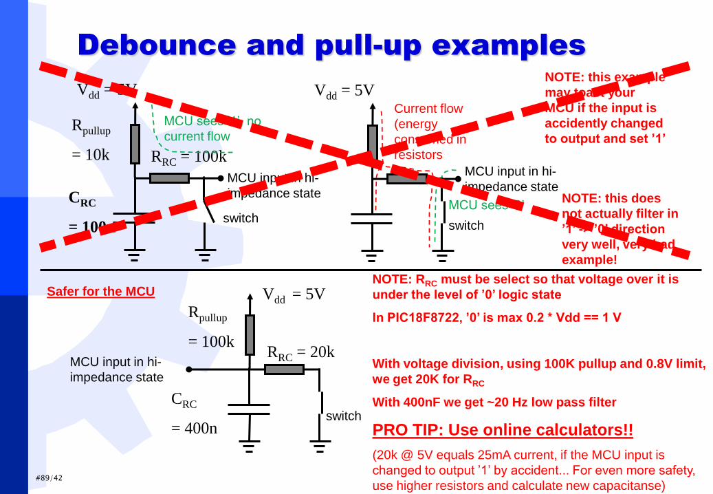
Debounce and pull-up examples
Vdd = 5V
Rpullup
= 10k
CRC
= 100n
switch
MCU input in hi-
impedance state
RRC = 100k
Vdd = 5V
switch
MCU sees ’1’, no
current flow
MCU sees ’0’
Current flow
(energy
consumed in
resistors
MCU input in hi-
impedance state
NOTE: this example
may toast your
MCU if the input is
accidently changed
to output and set ’1’
switch
MCU input in hi-
impedance state
Vdd = 5V
NOTE: RRC must be select so that voltage over it is
under the level of ’0’ logic state
In PIC18F8722, ’0’ is max 0.2 * Vdd == 1 V
With voltage division, using 100K pullup and 0.8V limit,
we get 20K for RRC
With 400nF we get ~20 Hz low pass filter
PRO TIP: Use online calculators!!
(20k @ 5V equals 25mA current, if the MCU input is
changed to output ’1’ by accident... For even more safety,
use higher resistors and calculate new capacitanse)
Rpullup
= 100k RRC = 20k
CRC
= 400n
Safer for the MCU
NOTE: this does
not actually filter in
’1’ -> ’0’ direction
very well, very bad
example!
#90/42
Very quick guide for MCU hobbyist (4)
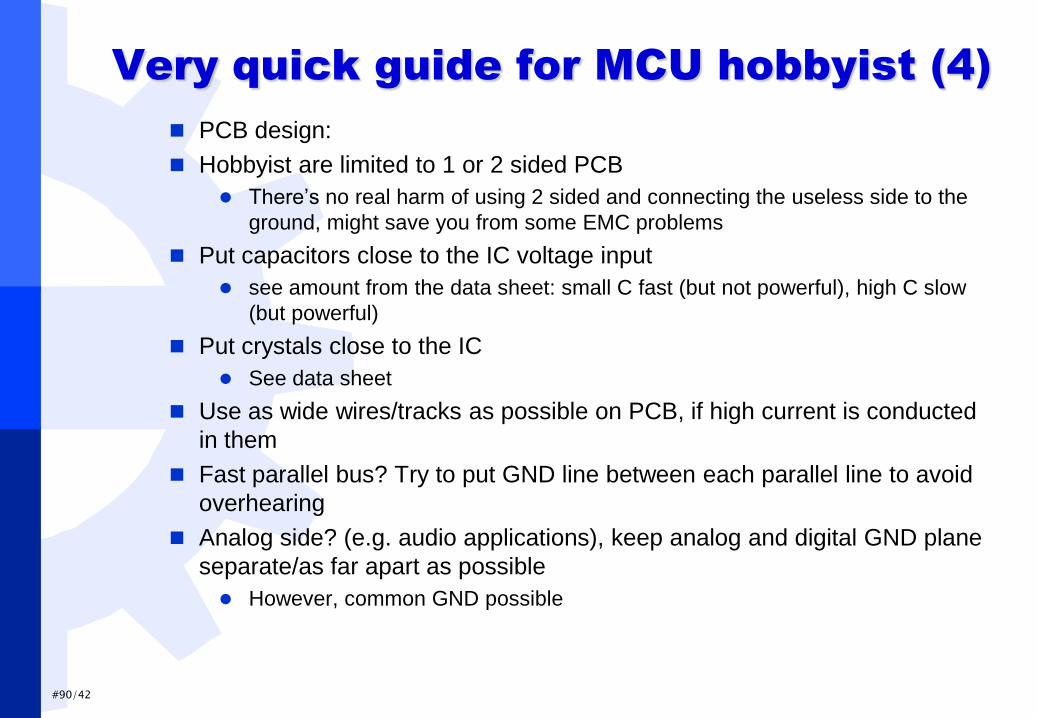
PCB design:
Hobbyist are limited to 1 or 2 sided PCB
There’s no real harm of using 2 sided and connecting the useless side to the
ground, might save you from some EMC problems
Put capacitors close to the IC voltage input
see amount from the data sheet: small C fast (but not powerful), high C slow
(but powerful)
Put crystals close to the IC
See data sheet
Use as wide wires/tracks as possible on PCB, if high current is conducted
in them
Fast parallel bus? Try to put GND line between each parallel line to avoid
overhearing
Analog side? (e.g. audio applications), keep analog and digital GND plane
separate/as far apart as possible
However, common GND possible
#91/42
Very quick guide for MCU hobbyist (5)
Soldering
Beware of cold solders, heat pads and legs
The tin should molt with touch to the to-be-connected
surfaces, not to the tip of the solder
Beware of overheating (IC) components
For example conduct heat to pincers
Rest is practice, practice, practice
http://www.youtube.com/watch?v=exOxUAntx8I
Internet is full of great (and bad) tips for how to solder,
e.g. surface mounted ICs
Do a mess and solder everything together, then use
”tinaimusukka” to remove excess tin
Use flux (juoksute) on pins, it will make soldering easier