1A, 1.2 MHz PWM Boost Converter in Thin SOT23 and DFN...
24
2018 Microchip Technology Inc. DS20006034B-page 1 MIC2288 Features • 2.5V to 10V Input Voltage Range • Output Voltage Adjustable to 34V • Over 1A Switch Current • 1.2 MHz PWM Operation • Stable with Ceramic Capacitors • <1% Line and Load Regulation • Low Output Voltage Ripple • <1 μA Shutdown Current • Undervoltage Lockout • Output Overvoltage Protection (MIC2288YML) • Overtemperature Shutdown • Thin SOT23-5 Package Option • 2 mm x 2 mm leadless DFN-8 Package Option • –40°C to +125°C Junction Temperature Range Applications • Organic EL Power Supply • TFT-LCD Bias Supply • 12V Supply for DSL Applications • Multi-Output DC/DC Converters • Positive and Negative Output Regulators • SEPIC Converters General Description The MIC2288 is a 1.2 MHz PWM, DC/DC boost switching regulator available in low-profile Thin SOT23 and 2 mm x 2 mm DFN package options. High power density is achieved with the MIC2288’s internal 34V/1A switch, allowing it to power large loads in a tiny footprint. The MIC2288 implements a constant frequency, 1.2 MHz PWM, current mode control scheme with internal compensation that offers excellent transient response and output regulation performance. The high frequency operation saves board space by allowing small, low-profile, external components. The fixed frequency PWM topology also reduces spurious switching noise and ripple to the input power source. The MIC2288 is available in a low-profile Thin SOT23-5 package and a 2 mm x 2 mm DFN-8 leadless package. The DFN package option has an output overvoltage protection feature. The MIC2288 has a junction temperature range of –40°C to +125°C. Package Types MIC2288 DFN-8 (ML) (Top View) MIC2288 Thin SOT23-5 (D5) (Top View) OVP VIN EN AGND PGND SW FB NC 1 2 3 4 8 7 6 5 EP FB GND EN VIN SW 3 1 5 2 4 1A, 1.2 MHz PWM Boost Converter in Thin SOT23 and DFN Packages
Transcript of 1A, 1.2 MHz PWM Boost Converter in Thin SOT23 and DFN...

2018 Microchip Technology Inc. DS20006034B-page 1
MIC2288
Features
• 2.5V to 10V Input Voltage Range
• Output Voltage Adjustable to 34V
• Over 1A Switch Current
• 1.2 MHz PWM Operation
• Stable with Ceramic Capacitors
• <1% Line and Load Regulation
• Low Output Voltage Ripple
• <1 µA Shutdown Current
• Undervoltage Lockout
• Output Overvoltage Protection (MIC2288YML)
• Overtemperature Shutdown
• Thin SOT23-5 Package Option
• 2 mm x 2 mm leadless DFN-8 Package Option
• –40°C to +125°C Junction Temperature Range
Applications• Organic EL Power Supply
• TFT-LCD Bias Supply
• 12V Supply for DSL Applications
• Multi-Output DC/DC Converters
• Positive and Negative Output Regulators
• SEPIC Converters
General Description
The MIC2288 is a 1.2 MHz PWM, DC/DC boostswitching regulator available in low-profile Thin SOT23and 2 mm x 2 mm DFN package options. High powerdensity is achieved with the MIC2288’s internal 34V/1Aswitch, allowing it to power large loads in a tinyfootprint.
The MIC2288 implements a constant frequency,1.2 MHz PWM, current mode control scheme withinternal compensation that offers excellent transientresponse and output regulation performance. The highfrequency operation saves board space by allowingsmall, low-profile, external components. The fixedfrequency PWM topology also reduces spuriousswitching noise and ripple to the input power source.
The MIC2288 is available in a low-profile Thin SOT23-5package and a 2 mm x 2 mm DFN-8 leadless package.The DFN package option has an output overvoltageprotection feature.
The MIC2288 has a junction temperature range of –40°C to +125°C.
Package TypesMIC2288
DFN-8 (ML)(Top View)
MIC2288Thin SOT23-5 (D5)
(Top View)
OVP
VIN
EN
AGND
PGND
SW
FB
NC
1
2
3
4
8
7
6
5EP
FB GND
EN VIN
SW3 1
5
2
4
1A, 1.2 MHz PWM Boost Converter in Thin SOT23 and DFN Packages
MIC2288
DS20006034B-page 2 2018 Microchip Technology Inc.
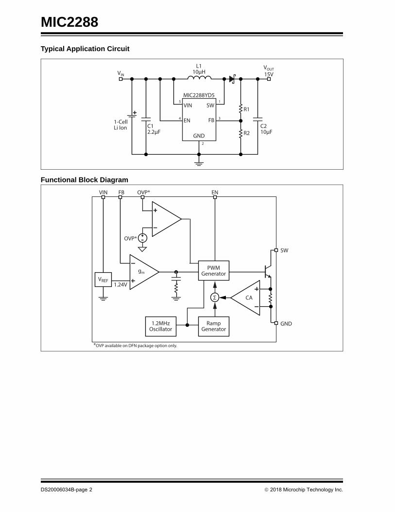
Typical Application Circuit
Functional Block Diagram
2
L110μH
R2
R13
1
4
5
MIC2288YD5
VIN
1-CellLi Ion
VOUT
15V
EN
SW
FB
GND
VIN
C12.2μF
C210μF
GND
CA
PWMGenerator
RampGenerator
1.2MHzOscillator
SW
ENFB OVP*VIN
1.24V
*OVP available on DFN package option only.
gm
OVP*
Σ
VREF
2018 Microchip Technology Inc. DS20006034B-page 3
MIC2288
1.0 ELECTRICAL CHARACTERISTICS
Absolute Maximum Ratings †
Supply Voltage (VIN) .................................................................................................................................................+12VSwitch Voltage (VSW) ................................................................................................................................. –0.3V to +34VEnable Pin Voltage (VEN) ...............................................................................................................................–0.3V to VINFB Voltage (VFB) ......................................................................................................................................................+6.0VSwitch Current (ISW) .....................................................................................................................................................2AESD Rating (Note 1) ................................................................................................................................................+2 kV
Operating Ratings ††
Supply Voltage (VIN) .................................................................................................................................. +2.5V to +10V
† Notice: Stresses above those listed under “Absolute Maximum Ratings” may cause permanent damage to the device.This is a stress rating only and functional operation of the device at those or any other conditions above those indicatedin the operational sections of this specification is not intended. Exposure to maximum rating conditions for extendedperiods may affect device reliability.
†† Notice: The device is not guaranteed to function outside its operating ratings.
Note 1: Devices are ESD sensitive. Handling precautions are recommended. Human body model, 1.5 kΩ in serieswith 100 pF.
MIC2288
DS20006034B-page 4 2018 Microchip Technology Inc.
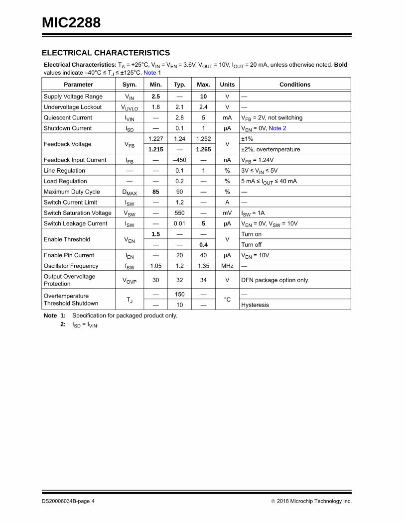
ELECTRICAL CHARACTERISTICS
Electrical Characteristics: TA = +25°C, VIN = VEN = 3.6V, VOUT = 10V, IOUT = 20 mA, unless otherwise noted. Bold values indicate –40°C ≤ TJ ≤ ±125°C. Note 1
Parameter Sym. Min. Typ. Max. Units Conditions
Supply Voltage Range VIN 2.5 — 10 V —
Undervoltage Lockout VUVLO 1.8 2.1 2.4 V —
Quiescent Current IVIN — 2.8 5 mA VFB = 2V, not switching
Shutdown Current ISD — 0.1 1 µA VEN = 0V, Note 2
Feedback Voltage VFB
1.227 1.24 1.252V
±1%
1.215 — 1.265 ±2%, overtemperature
Feedback Input Current IFB — –450 — nA VFB = 1.24V
Line Regulation — — 0.1 1 % 3V ≤ VIN ≤ 5V
Load Regulation — — 0.2 — % 5 mA ≤ IOUT ≤ 40 mA
Maximum Duty Cycle DMAX 85 90 — % —
Switch Current Limit ISW — 1.2 — A —
Switch Saturation Voltage VSW — 550 — mV ISW = 1A
Switch Leakage Current ISW — 0.01 5 µA VEN = 0V, VSW = 10V
Enable Threshold VEN
1.5 — —V
Turn on
— — 0.4 Turn off
Enable Pin Current IEN — 20 40 µA VEN = 10V
Oscillator Frequency fSW 1.05 1.2 1.35 MHz —
Output Overvoltage Protection
VOVP 30 32 34 V DFN package option only
Overtemperature Threshold Shutdown
TJ
— 150 —°C
—
— 10 — Hysteresis
Note 1: Specification for packaged product only.
2: ISD = IVIN.
2018 Microchip Technology Inc. DS20006034B-page 5
MIC2288
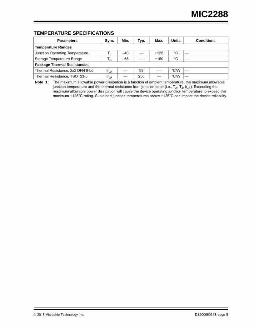
TEMPERATURE SPECIFICATIONS
Parameters Sym. Min. Typ. Max. Units Conditions
Temperature Ranges
Junction Operating Temperature TJ –40 — +125 °C —
Storage Temperature Range TS –65 — +150 °C —
Package Thermal Resistances
Thermal Resistance, 2x2 DFN 8-Ld JA — 93 — °C/W —
Thermal Resistance, TSOT23-5 JA — 256 — °C/W —
Note 1: The maximum allowable power dissipation is a function of ambient temperature, the maximum allowable junction temperature and the thermal resistance from junction to air (i.e., TA, TJ, JA). Exceeding the maximum allowable power dissipation will cause the device operating junction temperature to exceed the maximum +125°C rating. Sustained junction temperatures above +125°C can impact the device reliability.
MIC2288
DS20006034B-page 6 2018 Microchip Technology Inc.
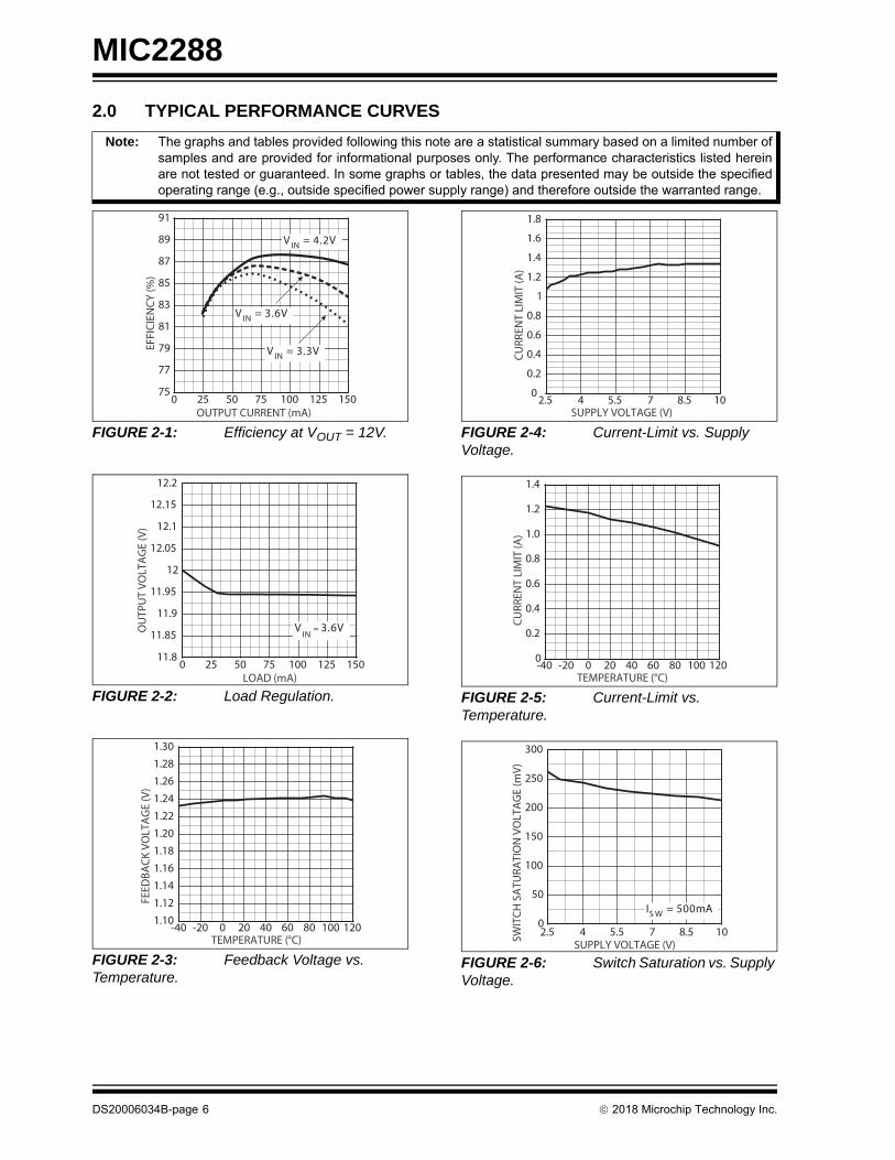
2.0 TYPICAL PERFORMANCE CURVES
FIGURE 2-1: Efficiency at VOUT = 12V.
FIGURE 2-2: Load Regulation.
FIGURE 2-3: Feedback Voltage vs. Temperature.
FIGURE 2-4: Current-Limit vs. Supply Voltage.
FIGURE 2-5: Current-Limit vs. Temperature.
FIGURE 2-6: Switch Saturation vs. Supply Voltage.
Note: The graphs and tables provided following this note are a statistical summary based on a limited number ofsamples and are provided for informational purposes only. The performance characteristics listed hereinare not tested or guaranteed. In some graphs or tables, the data presented may be outside the specifiedoperating range (e.g., outside specified power supply range) and therefore outside the warranted range.
75
77
79
81
83
85
87
89
91
0 25 50 75 100 125 150
EFFI
CIE
NC
Y (%
)
OUTPUT CURRENT (mA)
V IN = 4.2V
V IN = 3.6V
V IN = 3.3V
11.8
11.85
11.9
11.95
12
12.05
12.1
12.15
12.2
0 25 50 75 100 125 150
OU
TPU
T VO
LTA
GE
(V)
LOAD (mA)
VIN
= 3.6V
1.10
1.12
1.14
1.16
1.18
1.20
1.22
1.24
1.26
1.28
1.30
-40 -20 0 20 40 60 80 100 120
FEED
BAC
K VO
LTA
GE
(V)
TEMPERATURE (°C)
0
0.2
0.4
0.6
0.8
1
1.2
1.4
1.6
1.8
2.5 4 5.5 7 8.5 10
CU
RREN
T LI
MIT
(A)
SUPPLY VOLTAGE (V)
0
0.2
0.4
0.6
0.8
1.0
1.2
1.4
-40 -20 0 20 40 60 80 100 120
CU
RREN
T LI
MIT
(A)
TEMPERATURE (°C)
0
50
100
150
200
250
300
2.5 4 5.5 7 8.5 10SWIT
CH
SA
TURA
TIO
N V
OLT
AG
E (m
V)
SUPPLY VOLTAGE (V)
IS W = 500mA
2018 Microchip Technology Inc. DS20006034B-page 7
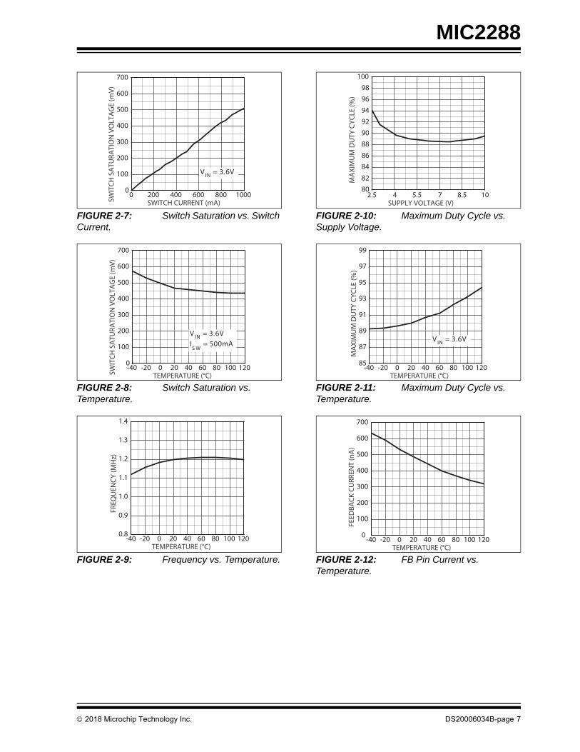
MIC2288
FIGURE 2-7: Switch Saturation vs. Switch Current.
FIGURE 2-8: Switch Saturation vs. Temperature.
FIGURE 2-9: Frequency vs. Temperature.
.
FIGURE 2-10: Maximum Duty Cycle vs. Supply Voltage.
FIGURE 2-11: Maximum Duty Cycle vs. Temperature.
FIGURE 2-12: FB Pin Current vs. Temperature.
0
100
200
300
400
500
600
700
0 200 400 600 800 1000
SWIT
CH
SA
TURA
TIO
N V
OLT
AG
E (m
V)
SWITCH CURRENT (mA)
V IN = 3.6V
0
100
200
300
400
500
600
700
-40 -20 0 20 40 60 80 100 120
SWIT
CH
SA
TURA
TIO
N V
OLT
AG
E (m
V)
TEMPERATURE (°C)
V IN = 3.6VIS W
= 500mA
0.8
0.9
1.0
1.1
1.2
1.3
1.4
-40 -20 0 20 40 60 80 100 120
FREQ
UEN
CY
(MH
z)
TEMPERATURE (°C)
80
82
84
86
88
90
92
94
96
98
100
2.5 4 5.5 7 8.5 10
MA
XIM
UM
DU
TY C
YCLE
(%)
SUPPLY VOLTAGE (V)
85
87
89
91
93
95
97
99
-40 -20 0 20 40 60 80 100 120
MA
XIM
UM
DU
TY C
YCLE
(%)
TEMPERATURE (°C)
V IN = 3.6V
0
100
200
300
400
500
600
700
-40 -20 0 20 40 60 80 100 120
FEED
BAC
K C
URR
ENT
(nA
)
TEMPERATURE (°C)
MIC2288
DS20006034B-page 8 2018 Microchip Technology Inc.
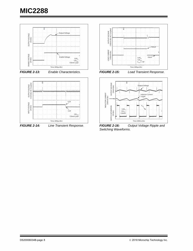
FIGURE 2-13: Enable Characteristics.
FIGURE 2-14: Line Transient Response.
FIGURE 2-15: Load Transient Response.
FIGURE 2-16: Output Voltage Ripple and Switching Waveforms.
Time (400μs/div)
OU
TPU
T VO
LTA
GE
(5V/
div)
ENA
BLE
VOLT
AG
E(2
V/di
v) 3.6VIN
12VOUT
150mA Load
Output Voltage
Enable Voltage
Time (400μs/div)
OU
TPU
T VO
LTA
GE
(1m
V/di
v) A
C-C
oupl
edIN
PUT
VOLT
AG
E(2
V/di
v)
4.2V
3.2V
12VOUT
150mA Load
Time (400μs/div)
OU
TPU
T VO
LTA
GE
(100
mV/
div)
AC
-Cou
pled
LOA
D C
URR
ENT
(100
mA
/div
)
10mA
150mA
3.6VIN
12VOUT
COUT = 10F
Time (400ns/div)
OU
TPU
T VO
LTA
GE
(50m
V/di
v)
IND
UC
TOR
CU
RREN
T(5
00m
A/d
iv)
SWIT
CH
SAT
URA
TIO
N(5
V/di
v)
VSW
Output Voltage
3.6VIN
12VOUT
150mA
Inductor Current(10μH)
2018 Microchip Technology Inc. DS20006034B-page 9
MIC2288
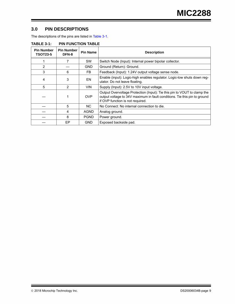
3.0 PIN DESCRIPTIONS
The descriptions of the pins are listed in Table 3-1.
TABLE 3-1: PIN FUNCTION TABLE
Pin NumberTSOT23-5
Pin NumberDFN-8
Pin Name Description
1 7 SW Switch Node (Input): Internal power bipolar collector.
2 — GND Ground (Return): Ground.
3 6 FB Feedback (Input): 1.24V output voltage sense node.
4 3 ENEnable (input): Logic-high enables regulator. Logic-low shuts down reg-ulator. Do not leave floating.
5 2 VIN Supply (Input): 2.5V to 10V input voltage.
— 1 OVPOutput Overvoltage Protection (Input): Tie this pin to VOUT to clamp the output voltage to 34V maximum in fault conditions. Tie this pin to ground if OVP function is not required.
— 5 NC No Connect: No internal connection to die.
— 4 AGND Analog ground.
— 8 PGND Power ground.
— EP GND Exposed backside pad.
MIC2288
DS20006034B-page 10 2018 Microchip Technology Inc.
4.0 FUNCTIONAL DESCRIPTION
The MIC2288 is a constant frequency, PWM currentmode boost regulator. See the Functional BlockDiagram. The MIC2288 is composed of an oscillator,slope compensation ramp generator, current amplifier,gm error amplifier, PWM generator, and a 1A bipolaroutput transistor. The oscillator generates a 1.2 MHzclock. The clock’s two functions are to trigger the PWMgenerator that turns on the output transistor and toreset the slope compensation ramp generator. Thecurrent amplifier is used to measure the switch currentby amplifying the voltage signal from the internal senseresistor. The output of the current amplifier is summedwith the output of the slope compensation rampgenerator. This summed current-loop signal is fed toone of the inputs of the PWM generator.
The gm error amplifier measures the feedback voltagethrough the external feedback resistors and amplifiesthe error between the detected signal and the 1.24Vreference voltage. The output of the gm error amplifierprovides the voltage-loop signal that is fed to the otherinput of the PWM generator. When the current-loopsignal exceeds the voltage-loop signal, the PWMgenerator turns off the bipolar output transistor. Thenext clock period initiates the next switching cycle,maintaining the constant frequency current-modePWM control.
2018 Microchip Technology Inc. DS20006034B-page 11
MIC2288
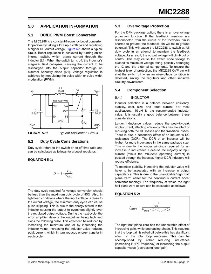
5.0 APPLICATION INFORMATION
5.1 DC/DC PWM Boost Conversion
The MIC2288 is a constant-frequency boost converter.It operates by taking a DC input voltage and regulatinga higher DC output voltage. Figure 5-1 shows a typicalcircuit. Boost regulation is achieved by turning on aninternal switch, which draws current through theinductor (L1). When the switch turns off, the inductor’smagnetic field collapses, causing the current to bedischarged into the output capacitor through anexternal Schottky diode (D1). Voltage regulation isachieved by modulating the pulse width or pulse-widthmodulation (PWM).
FIGURE 5-1: Typical Application Circuit.
5.2 Duty Cycle Considerations
Duty cycle refers to the switch on-to-off time ratio andcan be calculated as follows for a boost regulator:
EQUATION 5-1:
The duty cycle required for voltage conversion shouldbe less than the maximum duty cycle of 85%. Also, inlight load conditions where the input voltage is close tothe output voltage, the minimum duty cycle can causepulse skipping. This is due to the energy stored in theinductor causing the output to overshoot slightly overthe regulated output voltage. During the next cycle, theerror amplifier detects the output as being high andskips the following pulse. This effect can be reduced byincreasing the minimum load or by increasing theinductor value. Increasing the inductor value reducespeak current, which in turn reduces energy transfer ineach cycle.
5.3 Overvoltage Protection
For the DFN package option, there is an overvoltageprotection function. If the feedback resistors aredisconnected from the circuit or the feedback pin isshorted to ground, the feedback pin will fall to groundpotential. This will cause the MIC2288 to switch at fullduty cycle in an attempt to maintain the feedbackvoltage. As a result, the output voltage will climb out ofcontrol. This may cause the switch node voltage toexceed its maximum voltage rating, possibly damagingthe IC and the external components. To ensure thehighest level of protection, the MIC2288 OVP pin willshut the switch off when an overvoltage condition isdetected, saving the regulator and other sensitivecircuitry downstream.
5.4 Component Selection
5.4.1 INDUCTOR
Inductor selection is a balance between efficiency,stability, cost, size, and rated current. For mostapplications, 10 μH is the recommended inductorvalue. It is usually a good balance between theseconsiderations.
Larger inductance values reduce the peak-to-peakripple current, affecting efficiency. This has the effect ofreducing both the DC losses and the transition losses.There is also a secondary effect of an inductor’s DCresistance (DCR). The DCR of an inductor will behigher for more inductance in the same package size.This is due to the longer windings required for anincrease in inductance. Because the majority of inputcurrent (minus the MIC2288 operating current) ispassed through the inductor, higher DCR inductors willreduce efficiency.
To maintain stability, increasing the inductor value willhave to be associated with an increase in outputcapacitance. This is due to the unavoidable “right halfplane zero” effect for the continuous current boostconverter topology. The frequency at which the righthalf plane zero occurs can be calculated as follows:
EQUATION 5-2:
The right half plane zero has the undesirable effect ofincreasing gain, while decreasing phase. This requiresthat the loop gain is rolled off before this has significanteffect on the total loop response. This can beaccomplished by either reducing inductance(increasing RHPZ frequency) or increasing the outputcapacitor value (decreasing loop gain).
L110μH
C210μF
R2
R1
MIC2288YML
VIN
VIN VOUT
EN
SW
FBGND
GND
OVP
GND
C12.2μF
D1
D 1VIN
VOUT-------------–=
fRHPZ
VIN2
VOUT L IOUT 2-------------------------------------------------------=
MIC2288
DS20006034B-page 12 2018 Microchip Technology Inc.
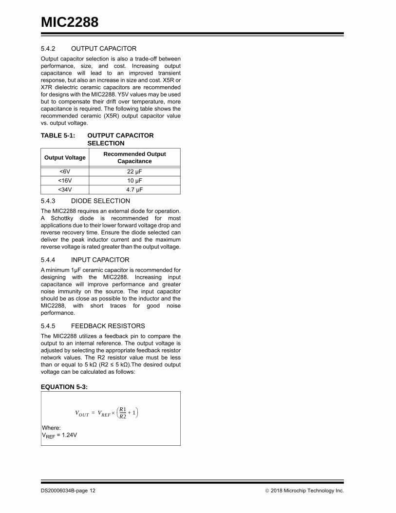
5.4.2 OUTPUT CAPACITOR
Output capacitor selection is also a trade-off betweenperformance, size, and cost. Increasing outputcapacitance will lead to an improved transientresponse, but also an increase in size and cost. X5R orX7R dielectric ceramic capacitors are recommendedfor designs with the MIC2288. Y5V values may be usedbut to compensate their drift over temperature, morecapacitance is required. The following table shows therecommended ceramic (X5R) output capacitor valuevs. output voltage.
5.4.3 DIODE SELECTION
The MIC2288 requires an external diode for operation.A Schottky diode is recommended for mostapplications due to their lower forward voltage drop andreverse recovery time. Ensure the diode selected candeliver the peak inductor current and the maximumreverse voltage is rated greater than the output voltage.
5.4.4 INPUT CAPACITOR
A minimum 1μF ceramic capacitor is recommended fordesigning with the MIC2288. Increasing inputcapacitance will improve performance and greaternoise immunity on the source. The input capacitorshould be as close as possible to the inductor and theMIC2288, with short traces for good noiseperformance.
5.4.5 FEEDBACK RESISTORS
The MIC2288 utilizes a feedback pin to compare theoutput to an internal reference. The output voltage isadjusted by selecting the appropriate feedback resistornetwork values. The R2 resistor value must be lessthan or equal to 5 kΩ (R2 ≤ 5 kΩ).The desired outputvoltage can be calculated as follows:
EQUATION 5-3:
TABLE 5-1: OUTPUT CAPACITOR SELECTION
Output VoltageRecommended Output
Capacitance
<6V 22 µF
<16V 10 µF
<34V 4.7 µF
VOUT VREFR1R2------- 1+ =
Where:VREF = 1.24V
2018 Microchip Technology Inc. DS20006034B-page 13
MIC2288
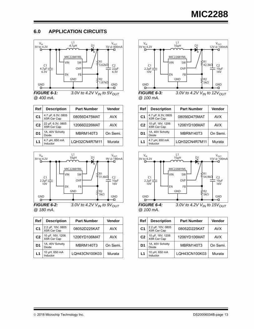
6.0 APPLICATION CIRCUITS
FIGURE 6-1: 3.0V to 4.2V VIN to 5VOUT @ 400 mA.
FIGURE 6-2: 3.0V to 4.2V VIN to 9VOUT @ 180 mA.
FIGURE 6-3: 3.0V to 4.2V VIN to 12VOUT @ 100 mA.
FIGURE 6-4: 3.0V to 4.2V VIN to 15VOUT @ 100 mA.
Ref Description Part Number Vendor
C1 4.7 µF, 6.3V, 0805 X5R Cer Cap 08056D475MAT AVX
C2 22 µF, 6.3V, 0805 X5R Cer Cap 12066D226MAT AVX
D1 1A, 40V Schotty Diode MBRM140T3 On Semi.
L1 4.7 µH, 650 mA Inductor LQH32CN4R7M11 Murata
Ref Description Part Number Vendor
C1 2.2 µF, 10V, 0805 X5R Cer Cap 08052D225KAT AVX
C2 10 µF, 16V, 1206 X5R Cer Cap 1206YD106MAT AVX
D1 1A, 40V Schotty Diode MBRM140T3 On Semi.
L1 10 µH, 650 mA Inductor LQH43CN100K03 Murata
L14.7μH
C222μF6.3V
R21.87kΩ
R15.62kΩ
MIC2288YML
VIN
VIN3V to 4.2V
VOUT5V @ 400mA
EN
SW
FBGND
GND
OVP
GND
C14.7μF
6.3V
D1
L110μH
C210μF16V
R25kΩ
R131.6kΩ
MIC2288YML
VIN
VIN3V to 4.2V
VOUT9V @ 180mA
EN
SW
FBGND
GND
OVP
GND
C12.2μF
10V
D1
Ref Description Part Number Vendor
C1 4.7 µF, 6.3V, 0805 X5R Cer Cap 08056D475MAT AVX
C2 10 µF, 16V, 1206 X5R Cer Cap 1206YD106MAT AVX
D1 1A, 40V Schotty Diode MBRM140T3 On Semi.
L1 4.7 µH, 650 mA Inductor LQH32CN4R7M11 Murata
Ref Description Part Number Vendor
C1 2.2 µF, 10V, 0805 X5R Cer Cap 08052D225KAT AVX
C2 10 µF, 16V, 1206 X5R Cer Cap 1206YD106MAT AVX
D1 1A, 40V Schotty Diode MBRM140T3 On Semi.
L1 10 µH, 650 mA Inductor LQH43CN100K03 Murata
L110μH
C210μF16V
R25kΩ
R142.3kΩ
MIC2288YML
VIN
VIN3V to 4.2V
VOUT12V @ 100mA
EN
SW
FBGND
GND
OVP
GND
C12.2μF
10V
D1
L110μH
C210μF16V
R25kΩ
R154.9kΩ
MIC2288YML
VIN
VIN3V to 4.2V
VOUT15V @ 100mA
EN
SW
FBGND
GND
OVP
GND
C12.2μF
10V
D1
MIC2288
DS20006034B-page 14 2018 Microchip Technology Inc.
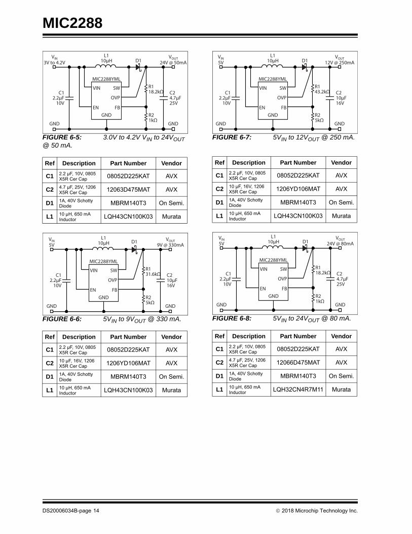
FIGURE 6-5: 3.0V to 4.2V VIN to 24VOUT @ 50 mA.
FIGURE 6-6: 5VIN to 9VOUT @ 330 mA.
FIGURE 6-7: 5VIN to 12VOUT @ 250 mA.
FIGURE 6-8: 5VIN to 24VOUT @ 80 mA.
Ref Description Part Number Vendor
C1 2.2 µF, 10V, 0805 X5R Cer Cap 08052D225KAT AVX
C2 4.7 µF, 25V, 1206 X5R Cer Cap 12063D475MAT AVX
D1 1A, 40V Schotty Diode MBRM140T3 On Semi.
L1 10 µH, 650 mA Inductor LQH43CN100K03 Murata
Ref Description Part Number Vendor
C1 2.2 µF, 10V, 0805 X5R Cer Cap 08052D225KAT AVX
C2 10 µF, 16V, 1206 X5R Cer Cap 1206YD106MAT AVX
D1 1A, 40V Schotty Diode MBRM140T3 On Semi.
L1 10 µH, 650 mA Inductor LQH43CN100K03 Murata
L110μH
C24.7μF25V
R21kΩ
R118.2kΩ
MIC2288YML
VIN
VIN3V to 4.2V
VOUT24V @ 50mA
EN
SW
FBGND
GND
OVP
GND
C12.2μF
10V
D1
L110μH
C210μF16V
R25kΩ
R131.6kΩ
MIC2288YML
VIN
VIN5V
VOUT9V @ 330mA
EN
SW
FBGND
GND
OVP
GND
C12.2μF
10V
D1
Ref Description Part Number Vendor
C1 2.2 µF, 10V, 0805 X5R Cer Cap 08052D225KAT AVX
C2 10 µF, 16V, 1206 X5R Cer Cap 1206YD106MAT AVX
D1 1A, 40V Schotty Diode MBRM140T3 On Semi.
L1 10 µH, 650 mA Inductor LQH43CN100K03 Murata
Ref Description Part Number Vendor
C1 2.2 µF, 10V, 0805 X5R Cer Cap 08052D225KAT AVX
C2 4.7 µF, 25V, 1206 X5R Cer Cap 12066D475MAT AVX
D1 1A, 40V Schotty Diode MBRM140T3 On Semi.
L1 10 µH, 650 mA Inductor LQH32CN4R7M11 Murata
L110μH
C210μF16V
R25kΩ
R143.2kΩ
MIC2288YML
VIN
VIN5V
VOUT12V @ 250mA
EN
SW
FBGND
GND
OVP
GND
C12.2μF
10V
D1
L110μH
C24.7μF25V
R21kΩ
R118.2kΩ
MIC2288YML
VIN
VIN5V
VOUT24V @ 80mA
EN
SW
FBGND
GND
OVP
GND
C12.2μF
10V
D1
2018 Microchip Technology Inc. DS20006034B-page 15
MIC2288
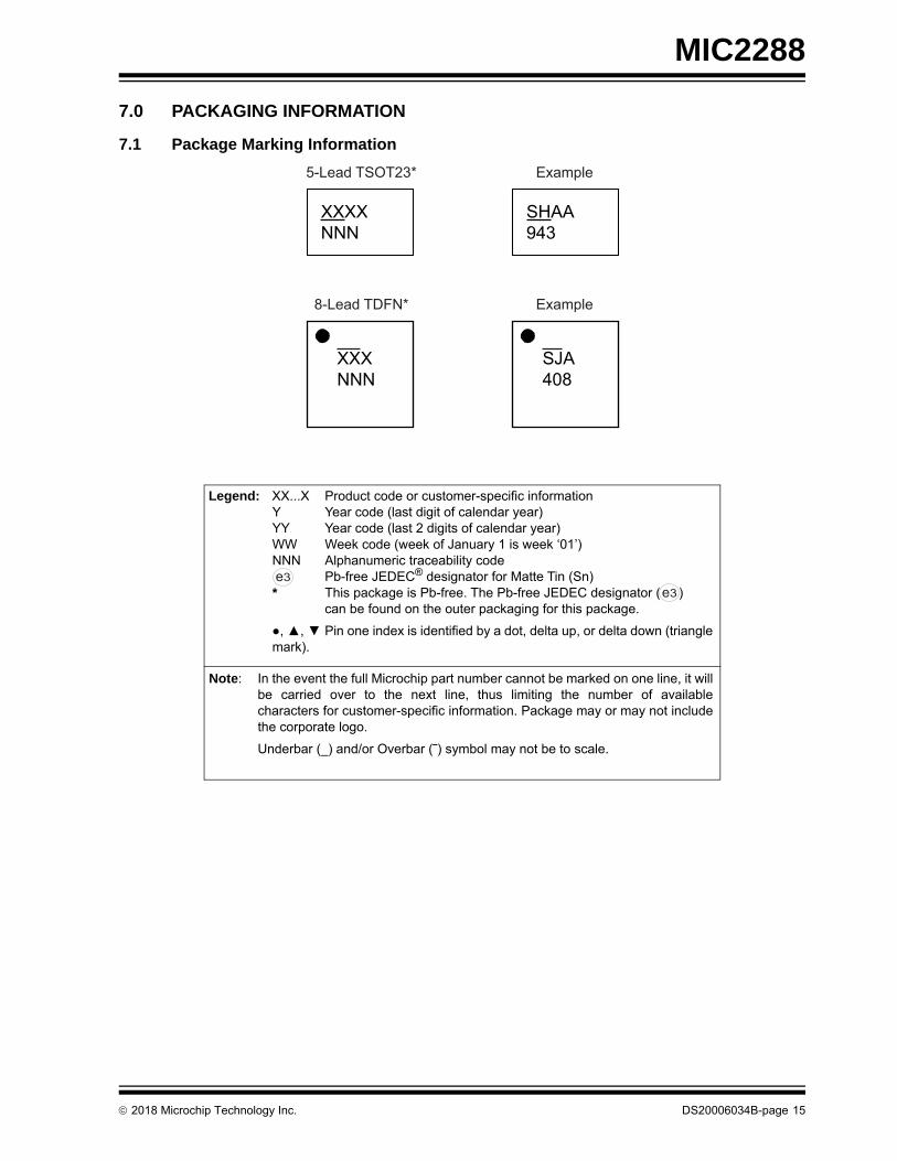
7.0 PACKAGING INFORMATION
7.1 Package Marking Information
Example8-Lead TDFN*
XXXNNN
SJA408
Example5-Lead TSOT23*
XXXXNNN
SHAA943
Legend: XX...X Product code or customer-specific informationY Year code (last digit of calendar year)YY Year code (last 2 digits of calendar year)WW Week code (week of January 1 is week ‘01’)NNN Alphanumeric traceability code Pb-free JEDEC® designator for Matte Tin (Sn)* This package is Pb-free. The Pb-free JEDEC designator ( )
can be found on the outer packaging for this package.
, , Pin one index is identified by a dot, delta up, or delta down (trianglemark).
Note: In the event the full Microchip part number cannot be marked on one line, it willbe carried over to the next line, thus limiting the number of availablecharacters for customer-specific information. Package may or may not includethe corporate logo.
Underbar (_) and/or Overbar (⎯) symbol may not be to scale.
3e
3e
MIC2288
DS20006034B-page 16 2018 Microchip Technology Inc.
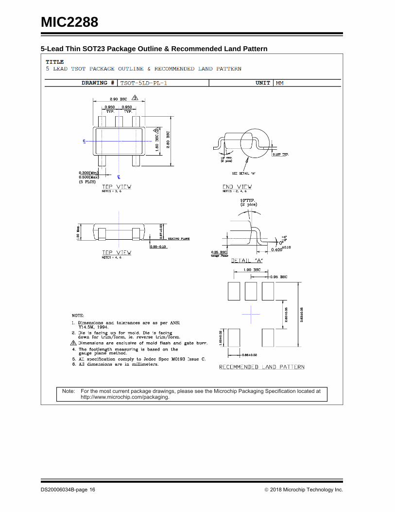
5-Lead Thin SOT23 Package Outline & Recommended Land Pattern
Note: For the most current package drawings, please see the Microchip Packaging Specification located at http://www.microchip.com/packaging.
2018 Microchip Technology Inc. DS20006034B-page 17
MIC2288
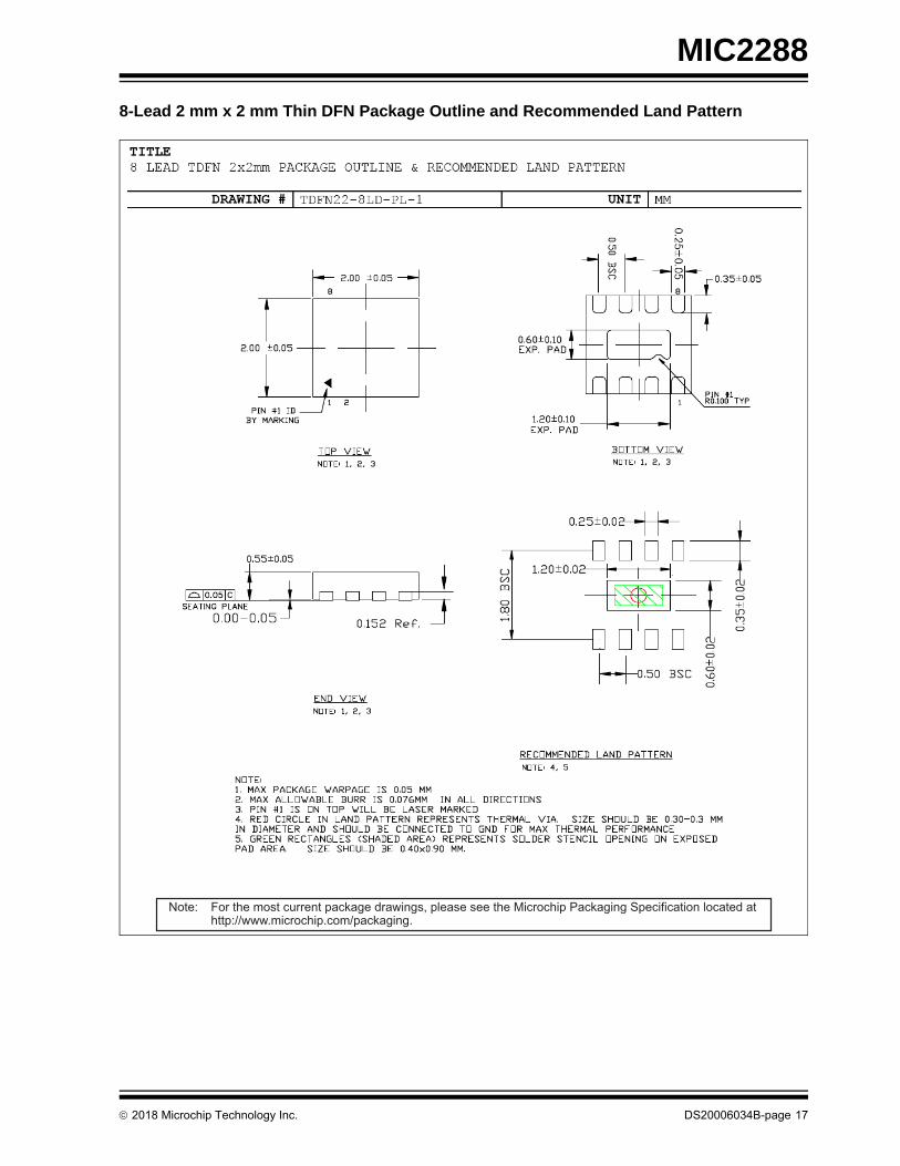
8-Lead 2 mm x 2 mm Thin DFN Package Outline and Recommended Land Pattern
Note: For the most current package drawings, please see the Microchip Packaging Specification located at http://www.microchip.com/packaging.

MIC2288
DS20006034B-page 18 2018 Microchip Technology Inc.
NOTES:
2018 Microchip Technology Inc. DS20006034B-page 19
MIC2288
APPENDIX A: REVISION HISTORY
Revision A (May 2018)
• Converted Micrel document MIC2288 to Micro-chip data sheet template DS20006034A.
• Minor grammatical text changes throughout.
• Updated Low Output Voltage Ripple in Features.
• Added clarification to EN description in Table 3-1.
• Updated drawing for EN in Figure 5-1.
• Updated drawings and figure captions for each entry in Section 6.0 “Application Circuits”.
Revision B (September 2018)
• Updated values for C2 in the table beneath Figure 6-3.

MIC2288
DS20006034B-page 20 2018 Microchip Technology Inc.
NOTES:
2018 Microchip Technology Inc. DS20006034B-page 21
MIC2288
PRODUCT IDENTIFICATION SYSTEM
To order or obtain information, e.g., on pricing or delivery, contact your local Microchip representative or sales office.
Examples:
a) MIC2288YD5-TX: MIC2288, –40°C to +125°CTemperature Range, 5-LeadTSOT23, 3,000/Reel (Reverse T/R)
b) MIC2288YD5-TR: MIC2288, –40°C to +125°CTemperature Range, 5-LeadTSOT, 3,000/Reel
c) MIC2288YML-TR: MIC2288, –40°C to +125°CTemperature Range, 8-LeadTDFN, 5,000/Reel
Device: MIC2288: 1A, 1.2 MHz PWM Boost Converter
Junction Temperature Range:
Y = –40°C to +125°C, RoHS-Compliant
Package:D5 = 5-Lead Thin SOT23ML = 8-Lead 2 mm x 2 mm TDFN
Media Type:TX = 3,000/Reel (Reverse T/R, TSOT only)TR = 3,000/Reel (TSOT only)TR = 5,000/Reel (TDFN only)
Note 1: Tape and Reel identifier only appears in the catalog part number description. This identifier is used for ordering purposes and is not printed on the device package. Check with your Microchip Sales Office for package availability with the Tape and Reel option.
Device X XX -XX
Part No. Junction Temp. Range
Package Media Type
MIC2288
DS20006034B-page 22 2018 Microchip Technology Inc.
NOTES:
2018 Microchip Technology Inc. DS20006034B-page 23
Information contained in this publication regarding deviceapplications and the like is provided only for your convenienceand may be superseded by updates. It is your responsibility toensure that your application meets with your specifications.MICROCHIP MAKES NO REPRESENTATIONS ORWARRANTIES OF ANY KIND WHETHER EXPRESS ORIMPLIED, WRITTEN OR ORAL, STATUTORY OROTHERWISE, RELATED TO THE INFORMATION,INCLUDING BUT NOT LIMITED TO ITS CONDITION,QUALITY, PERFORMANCE, MERCHANTABILITY ORFITNESS FOR PURPOSE. Microchip disclaims all liabilityarising from this information and its use. Use of Microchipdevices in life support and/or safety applications is entirely atthe buyer’s risk, and the buyer agrees to defend, indemnify andhold harmless Microchip from any and all damages, claims,suits, or expenses resulting from such use. No licenses areconveyed, implicitly or otherwise, under any Microchipintellectual property rights unless otherwise stated.
Trademarks
The Microchip name and logo, the Microchip logo, AnyRate, AVR, AVR logo, AVR Freaks, BitCloud, chipKIT, chipKIT logo, CryptoMemory, CryptoRF, dsPIC, FlashFlex, flexPWR, Heldo, JukeBlox, KeeLoq, Kleer, LANCheck, LINK MD, maXStylus, maXTouch, MediaLB, megaAVR, MOST, MOST logo, MPLAB, OptoLyzer, PIC, picoPower, PICSTART, PIC32 logo, Prochip Designer, QTouch, SAM-BA, SpyNIC, SST, SST Logo, SuperFlash, tinyAVR, UNI/O, and XMEGA are registered trademarks of Microchip Technology Incorporated in the U.S.A. and other countries.
ClockWorks, The Embedded Control Solutions Company, EtherSynch, Hyper Speed Control, HyperLight Load, IntelliMOS, mTouch, Precision Edge, and Quiet-Wire are registered trademarks of Microchip Technology Incorporated in the U.S.A.
Adjacent Key Suppression, AKS, Analog-for-the-Digital Age, Any Capacitor, AnyIn, AnyOut, BodyCom, CodeGuard, CryptoAuthentication, CryptoAutomotive, CryptoCompanion, CryptoController, dsPICDEM, dsPICDEM.net, Dynamic Average Matching, DAM, ECAN, EtherGREEN, In-Circuit Serial Programming, ICSP, INICnet, Inter-Chip Connectivity, JitterBlocker, KleerNet, KleerNet logo, memBrain, Mindi, MiWi, motorBench, MPASM, MPF, MPLAB Certified logo, MPLIB, MPLINK, MultiTRAK, NetDetach, Omniscient Code Generation, PICDEM, PICDEM.net, PICkit, PICtail, PowerSmart, PureSilicon, QMatrix, REAL ICE, Ripple Blocker, SAM-ICE, Serial Quad I/O, SMART-I.S., SQI, SuperSwitcher, SuperSwitcher II, Total Endurance, TSHARC, USBCheck, VariSense, ViewSpan, WiperLock, Wireless DNA, and ZENA are trademarks of Microchip Technology Incorporated in the U.S.A. and other countries.
SQTP is a service mark of Microchip Technology Incorporated in the U.S.A.
Silicon Storage Technology is a registered trademark of Microchip Technology Inc. in other countries.
GestIC is a registered trademark of Microchip Technology Germany II GmbH & Co. KG, a subsidiary of Microchip Technology Inc., in other countries.
All other trademarks mentioned herein are property of their respective companies.
© 2018, Microchip Technology Incorporated, All Rights Reserved.
ISBN: 978-1-5224-3533-4
Note the following details of the code protection feature on Microchip devices:
• Microchip products meet the specification contained in their particular Microchip Data Sheet.
• Microchip believes that its family of products is one of the most secure families of its kind on the market today, when used in the intended manner and under normal conditions.
• There are dishonest and possibly illegal methods used to breach the code protection feature. All of these methods, to our knowledge, require using the Microchip products in a manner outside the operating specifications contained in Microchip’s Data Sheets. Most likely, the person doing so is engaged in theft of intellectual property.
• Microchip is willing to work with the customer who is concerned about the integrity of their code.
• Neither Microchip nor any other semiconductor manufacturer can guarantee the security of their code. Code protection does not mean that we are guaranteeing the product as “unbreakable.”
Code protection is constantly evolving. We at Microchip are committed to continuously improving the code protection features of ourproducts. Attempts to break Microchip’s code protection feature may be a violation of the Digital Millennium Copyright Act. If such actsallow unauthorized access to your software or other copyrighted work, you may have a right to sue for relief under that Act.
Microchip received ISO/TS-16949:2009 certification for its worldwide headquarters, design and wafer fabrication facilities in Chandler and Tempe, Arizona; Gresham, Oregon and design centers in California and India. The Company’s quality system processes and procedures are for its PIC® MCUs and dsPIC® DSCs, KEELOQ® code hopping devices, Serial EEPROMs, microperipherals, nonvolatile memory and analog products. In addition, Microchip’s quality system for the design and manufacture of development systems is ISO 9001:2000 certified.
QUALITYMANAGEMENTSYSTEMCERTIFIEDBYDNV
== ISO/TS16949==
DS20006034B-page 24 2018 Microchip Technology Inc.
AMERICASCorporate Office2355 West Chandler Blvd.Chandler, AZ 85224-6199Tel: 480-792-7200 Fax: 480-792-7277Technical Support: http://www.microchip.com/supportWeb Address: www.microchip.com
AtlantaDuluth, GA Tel: 678-957-9614 Fax: 678-957-1455
Austin, TXTel: 512-257-3370
BostonWestborough, MA Tel: 774-760-0087 Fax: 774-760-0088
ChicagoItasca, IL Tel: 630-285-0071 Fax: 630-285-0075
DallasAddison, TX Tel: 972-818-7423 Fax: 972-818-2924
DetroitNovi, MI Tel: 248-848-4000
Houston, TX Tel: 281-894-5983
IndianapolisNoblesville, IN Tel: 317-773-8323Fax: 317-773-5453Tel: 317-536-2380
Los AngelesMission Viejo, CA Tel: 949-462-9523Fax: 949-462-9608Tel: 951-273-7800
Raleigh, NC Tel: 919-844-7510
New York, NY Tel: 631-435-6000
San Jose, CA Tel: 408-735-9110Tel: 408-436-4270
Canada - TorontoTel: 905-695-1980 Fax: 905-695-2078
ASIA/PACIFICAustralia - SydneyTel: 61-2-9868-6733
China - BeijingTel: 86-10-8569-7000
China - ChengduTel: 86-28-8665-5511
China - ChongqingTel: 86-23-8980-9588
China - DongguanTel: 86-769-8702-9880
China - GuangzhouTel: 86-20-8755-8029
China - HangzhouTel: 86-571-8792-8115
China - Hong Kong SARTel: 852-2943-5100
China - NanjingTel: 86-25-8473-2460
China - QingdaoTel: 86-532-8502-7355
China - ShanghaiTel: 86-21-3326-8000
China - ShenyangTel: 86-24-2334-2829
China - ShenzhenTel: 86-755-8864-2200
China - SuzhouTel: 86-186-6233-1526
China - WuhanTel: 86-27-5980-5300
China - XianTel: 86-29-8833-7252
China - XiamenTel: 86-592-2388138
China - ZhuhaiTel: 86-756-3210040
ASIA/PACIFICIndia - BangaloreTel: 91-80-3090-4444
India - New DelhiTel: 91-11-4160-8631
India - PuneTel: 91-20-4121-0141
Japan - OsakaTel: 81-6-6152-7160
Japan - TokyoTel: 81-3-6880- 3770
Korea - DaeguTel: 82-53-744-4301
Korea - SeoulTel: 82-2-554-7200
Malaysia - Kuala LumpurTel: 60-3-7651-7906
Malaysia - PenangTel: 60-4-227-8870
Philippines - ManilaTel: 63-2-634-9065
SingaporeTel: 65-6334-8870
Taiwan - Hsin ChuTel: 886-3-577-8366
Taiwan - KaohsiungTel: 886-7-213-7830
Taiwan - TaipeiTel: 886-2-2508-8600
Thailand - BangkokTel: 66-2-694-1351
Vietnam - Ho Chi MinhTel: 84-28-5448-2100
EUROPEAustria - WelsTel: 43-7242-2244-39Fax: 43-7242-2244-393
Denmark - CopenhagenTel: 45-4450-2828 Fax: 45-4485-2829
Finland - EspooTel: 358-9-4520-820
France - ParisTel: 33-1-69-53-63-20 Fax: 33-1-69-30-90-79
Germany - GarchingTel: 49-8931-9700
Germany - HaanTel: 49-2129-3766400
Germany - HeilbronnTel: 49-7131-67-3636
Germany - KarlsruheTel: 49-721-625370
Germany - MunichTel: 49-89-627-144-0 Fax: 49-89-627-144-44
Germany - RosenheimTel: 49-8031-354-560
Israel - Ra’anana Tel: 972-9-744-7705
Italy - Milan Tel: 39-0331-742611 Fax: 39-0331-466781
Italy - PadovaTel: 39-049-7625286
Netherlands - DrunenTel: 31-416-690399 Fax: 31-416-690340
Norway - TrondheimTel: 47-7288-4388
Poland - WarsawTel: 48-22-3325737
Romania - BucharestTel: 40-21-407-87-50
Spain - MadridTel: 34-91-708-08-90Fax: 34-91-708-08-91
Sweden - GothenbergTel: 46-31-704-60-40
Sweden - StockholmTel: 46-8-5090-4654
UK - WokinghamTel: 44-118-921-5800Fax: 44-118-921-5820
Worldwide Sales and Service
08/15/18