FAN100 Primary-Side-Control PWM Controller
16
January 2014 © 2009 Fairchild Semiconductor Corporation www.fairchildsemi.com FAN100 Rev. 1.0.3 FAN100 — Primary-Side-Control PWM Controller FAN100 Primary-Side-Control PWM Controller Features Constant-Voltage (CV) and Constant-Current (CC) Control without Secondary-Feedback Circuitry Accurate Constant Current Achieved by Fairchild’s Proprietary TRUECURRENT™ Technique Green Mode: Frequency Reduction at Light Load Fixed PWM Frequency at 42 kHz with Frequency Hopping to Reduce EMI Low Startup Current: 10 μA Maximum Low Operating Current: 3.5 mA Peak-Current-Mode Control in CV Mode Cycle-by-Cycle Current Limiting Over-Temperature Protection with Auto-Restart Brownout Protection with Auto-Restart VDD Over-Voltage Protection with Auto-Restart VDD Under-Voltage Lockout (UVLO) Gate Output Maximum Voltage Clamped at 18V SOP-8 Package Applications Battery Chargers for Cellular Phones, Cordless Phones, PDA, Digital Cameras, Power Tools Replaces Linear Transformer and RCC SMPS Offline High Brightness (HB) LED Drivers Related Resources Description AN-6067 — Design Guide for FAN100/102 and FSEZ1016A/1216 The primary-side PWM controller FAN100 significantly simplifies power supply design that requires CV and CC regulation capabilities. The FAN100 controls the output voltage and current precisely with the information in the primary side of the power supply, not only removing the output current sensing loss, but eliminating secondary feedback circuitry. The green-mode function with a low startup current (10μA) maximizes the light-load efficiency so the power supply can meet stringent standby power regulations. Compared with a conventional secondary-side regulation approach, the FAN100 can reduce total cost, component count, size, and weight; while simultaneously increasing efficiency, productivity, and system reliability. FAN100 controller is available in an 8-pin SOP package. A typical output CV/CC characteristic envelope is shown in Figure 1. V O I O Figure 1. Typical Output V-I Characteristic Ordering Information Part Number Operating Temperature Range Package Packing Method FAN100MY -40°C to +125°C 8-Lead, Small Outline Package (SOP-8) Tape & Reel For Fairchild’s definition of Eco Status, please visit: http://www.fairchildsemi.com/company/green/rohs_green.html .
Transcript of FAN100 Primary-Side-Control PWM Controller
January 2014
© 2009 Fairchild Semiconductor Corporation www.fairchildsemi.com FAN100 Rev. 1.0.3
FAN
100 — Prim
ary-Side-Control PW
M C
ontroller
FAN100 Primary-Side-Control PWM Controller Features Constant-Voltage (CV) and Constant-Current (CC)
Control without Secondary-Feedback Circuitry
Accurate Constant Current Achieved by Fairchild’s Proprietary TRUECURRENT™ Technique
Green Mode: Frequency Reduction at Light Load
Fixed PWM Frequency at 42 kHz with Frequency Hopping to Reduce EMI
Low Startup Current: 10 μA Maximum
Low Operating Current: 3.5 mA
Peak-Current-Mode Control in CV Mode
Cycle-by-Cycle Current Limiting
Over-Temperature Protection with Auto-Restart
Brownout Protection with Auto-Restart
VDD Over-Voltage Protection with Auto-Restart
VDD Under-Voltage Lockout (UVLO)
Gate Output Maximum Voltage Clamped at 18V
SOP-8 Package
Applications Battery Chargers for Cellular Phones, Cordless
Phones, PDA, Digital Cameras, Power Tools
Replaces Linear Transformer and RCC SMPS
Offline High Brightness (HB) LED Drivers
Related Resources
Description
AN-6067 — Design Guide for FAN100/102 and FSEZ1016A/1216
The primary-side PWM controller FAN100 significantly simplifies power supply design that requires CV and CC regulation capabilities. The FAN100 controls the output voltage and current precisely with the information in the primary side of the power supply, not only removing the output current sensing loss, but eliminating secondary feedback circuitry.
The green-mode function with a low startup current (10µA) maximizes the light-load efficiency so the power supply can meet stringent standby power regulations.
Compared with a conventional secondary-side regulation approach, the FAN100 can reduce total cost, component count, size, and weight; while simultaneously increasing efficiency, productivity, and system reliability.
FAN100 controller is available in an 8-pin SOP package.
A typical output CV/CC characteristic envelope is shown in Figure 1.
VO
IO
Figure 1. Typical Output V-I Characteristic
Ordering Information
Part Number Operating Temperature Range Package Packing Method
FAN100MY -40°C to +125°C 8-Lead, Small Outline Package (SOP-8) Tape & Reel
For Fairchild’s definition of Eco Status, please visit: http://www.fairchildsemi.com/company/green/rohs_green.html.
lhouse
POWI
© 2009 Fairchild Semiconductor Corporation www.fairchildsemi.com FAN100 Rev. 1.0.3 2
FAN
100 — Prim
ary-Side-Control PW
M C
ontroller
Application Diagram
NP NSRSN1 CSN1VDL
+
-
AC line
DSN
DR
CO
1
NACDD
Bridgerectifierdiode
VO
CDL
CS
GND
COMI
COMV
GATE
VDD
GND
VS
RSTART
RSN2CSN2
8
7
6
5
2
3
4
FAN100
IO
RS1
RS2
CS
RGATE
RCS
RCOMV
CCOMV
RCOMI
CCOMI
DDD
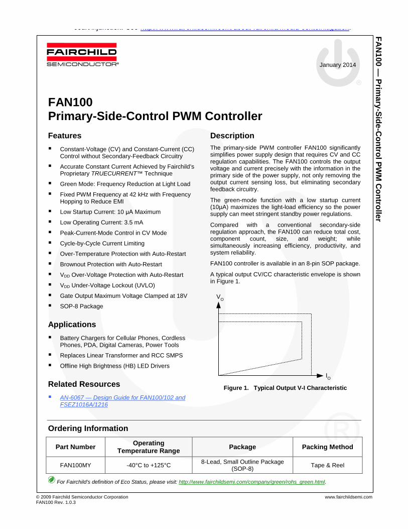
Figure 2. Typical Application
Internal Block Diagram
7
+
-16V/5V
Internal Bias
VDD
+
-
2
1
5
GND
VS
CS
OSC with Freq Hopping
28VBrownout
S
R
Q
Q
Green-Mode Controller
+
-
3COMI
+
-
+
-
1.3V
Leading-Edge Blanking
tDIS Detector
IO Estimator
VO Estimator
+
-
+
-
2.5VEA_I
EA_V
4COMV
Soft-Driver
8 Gate
VDD
Slope CompensationPWM
Comparator
PWM Comparator
PWM Comparator
6
Brownout Protection
GND Temp.Compensation
2.5V
Auto-RestartProtection
OTP
OVP
Figure 3. Functional Block Diagram
© 2009 Fairchild Semiconductor Corporation www.fairchildsemi.com FAN100 Rev. 1.0.3 3
FAN
100 — Prim
ary-Side-Control PW
M C
ontroller
Marking Information
1 2 3 4
8 6 5
ZXYTTFAN100
TPM7
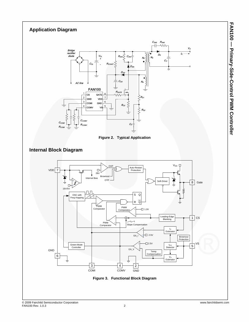
Figure 4. Top Mark
Pin Configuration
Figure 5. Pin Configuration
Pin Definitions
Pin # Name Description
1 CS Current Sense. This pin connects a current-sense resistor to sense the MOSFET current for peak-current-mode control in CV mode and provides for output-current regulation in CC mode.
2 GND Ground.
3 COMI Constant Current Loop Compensation. this pin connects a capacitor and a resistor between COMI and GND for compensation current loop gain.
4 COMV Constant Voltage Loop Compensation. this pin connects a capacitor and a resistor between COMV and GND for compensation voltage loop gain.
5 VS Voltage Sense. This pin detects the output voltage information and discharge time based on voltage of auxiliary winding. This pin connects two divider resistors and one capacitor.
6 GND Ground.
7 VDD
Supply. The power supply pin. IC operating current and MOSFET driving current are supplied using this pin. This pin is connected to an external VDD capacitor of typically 10 µF. The threshold voltages for startup and turn-off are 16 V and 5 V, respectively. The operating current is lower than 5 mA.
8 GATE PWM Signal Output. This pin outputs PWM signal and includes the internal totem-pole output driver to drive the external power MOSFET. The clamped gate output voltage is 18 V.
F- Fairchild logo Z- Plant Code X- 1-Digit Year Code Y- 1-Digit Week Code TT: 2-Digit Die Run Code T: Package Type (M=SOP) P: Z: Pb free, Y: Green Package M: Manufacture Flow Code
VS
GND
VDD
GATE
COMV
COMI
GND
CS
© 2009 Fairchild Semiconductor Corporation www.fairchildsemi.com FAN100 Rev. 1.0.3 4
FAN
100 — Prim
ary-Side-Control PW
M C
ontroller
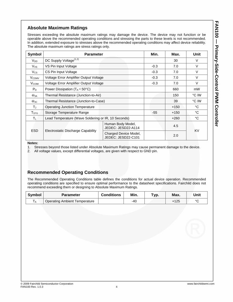
Absolute Maximum Ratings Stresses exceeding the absolute maximum ratings may damage the device. The device may not function or be operable above the recommended operating conditions and stressing the parts to these levels is not recommended. In addition, extended exposure to stresses above the recommended operating conditions may affect device reliability. The absolute maximum ratings are stress ratings only.
Symbol Parameter Min. Max. Unit VDD DC Supply Voltage(1,2) 30 V VVS VS Pin Input Voltage -0.3 7.0 V VCS CS Pin Input Voltage -0.3 7.0 V
VCOMV Voltage Error Amplifier Output Voltage -0.3 7.0 V VCOMI Voltage Error Amplifier Output Voltage -0.3 7.0 V
PD Power Dissipation (TA<50°C) 660 mW
ΘJA Thermal Resistance (Junction-to-Air) 150 °C /W
ΘJC Thermal Resistance (Junction-to-Case) 39 °C /W
TJ Operating Junction Temperature +150 °C TSTG Storage Temperature Range -55 +150 °C TL Lead Temperature (Wave Soldering or IR, 10 Seconds) +260 °C
ESD Electrostatic Discharge Capability
Human Body Model, JEDEC: JESD22-A114 4.5
KV Charged Device Model, JEDEC: JESD22-C101 2.0
Notes: 1. Stresses beyond those listed under Absolute Maximum Ratings may cause permanent damage to the device. 2. All voltage values, except differential voltages, are given with respect to GND pin.
Recommended Operating Conditions The Recommended Operating Conditions table defines the conditions for actual device operation. Recommended operating conditions are specified to ensure optimal performance to the datasheet specifications. Fairchild does not recommend exceeding them or designing to Absolute Maximum Ratings.
Symbol Parameter Conditions Min. Typ. Max. Unit TA Operating Ambient Temperature -40 +125 °C
© 2009 Fairchild Semiconductor Corporation www.fairchildsemi.com FAN100 Rev. 1.0.3 5
FAN
100 — Prim
ary-Side-Control PW
M C
ontroller
Electrical Characteristics VDD=15 V and TA=-40°C~+125°C (TA=TJ), unless otherwise specified.
Symbol Parameter Conditions Min. Typ. Max. Units VDD Section
VOP Continuously Operating Voltage 25 V
VDD-ON Turn-On Threshold Voltage 15 16 17 V
VDD-OFF Turn-Off Threshold Voltage 4.5 5.0 5.5 V
IDD-OP Operating Current VDD=20 V, fS=fOSC, VVS=2 V, VCS=3 V, CL=1 nF 3.5 5.0 mA
IDD-ST Startup Current 0< VDD < VDD-ON-0.16 V 3.7 10.0 μA
IDD-GREEN Green Mode Operating Supply Current
VDD=20 V, VVS=2.7 V, fS=fOSC-N-MIN, VCS=0 V, CL=1 nF, VCOMV=0 V
1.0 2.5 mA
VDD-OVP VDD Over-Voltage Protection Level VCS=3 V, VVS=2.3 V 27 28 29 V
tD-VDDOVP VDD Over-Voltage Protection Debounce Time fS=fOSC, VVS=2.3 V 100 250 400 μs
Oscillator Section
fOSC Frequency
Center Frequency TA=25°C 39.0 42.0 45.0
KHz Frequency Hopping Range TA=25°C ±1.8 ±2.6 ±3.6
tFHR Frequency Hopping Period TA=25°C 3 ms
fOSC-N-MIN Minimum Frequency at No Load VVS=2.7 V, VCOMV=0 V 550 Hz
fOSC-CM-MIN Minimum Frequency at CCM VVS=2.3 V, VCS=0.5 V 20 KHz
fDV Frequency Variation vs. VDD Deviation TA=25°C, VDD=10 V to 25 V 5 %
fDT Frequency Variation vs. Temperature Deviation TA=-40°C to 125°C 20 %
Voltage-Sense Section
IVS-UVP Sink Current for Brownout Protection RVS=20 KΩ 180 μA
Itc IC Compensation Bias Current 9.5 μA
VBIAS-COMV Adaptive Bias Voltage Dominated by VCOMV
VCOMV=0 V, TA=25°C, RVS=20 KΩ
1.4 V
Current-Sense Section
tPD Propagation Delay to GATE Output 100 200 ns
tMIN-N Minimum On Time at No Load VVS=-0.8 V, RS=2 KΩ, VCOMV=1 V
1100 ns
tMINCC Minimum On Time in CC Mode VVS=0 V, VCOMV=2 V 300 ns
VTH Threshold Voltage for Current Limit 1.3 V
Continued on following page…
© 2009 Fairchild Semiconductor Corporation www.fairchildsemi.com FAN100 Rev. 1.0.3 6
FAN
100 — Prim
ary-Side-Control PW
M C
ontroller
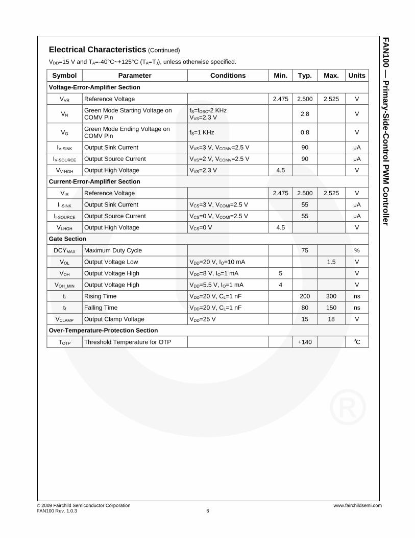
Electrical Characteristics (Continued)
VDD=15 V and TA=-40°C~+125°C (TA=TJ), unless otherwise specified.
Symbol Parameter Conditions Min. Typ. Max. Units Voltage-Error-Amplifier Section
VVR Reference Voltage 2.475 2.500 2.525 V
VN Green Mode Starting Voltage on COMV Pin
fS=fOSC-2 KHz VVS=2.3 V 2.8 V
VG Green Mode Ending Voltage on COMV Pin fS=1 KHz 0.8 V
IV-SINK Output Sink Current VVS=3 V, VCOMV=2.5 V 90 μA
IV-SOURCE Output Source Current VVS=2 V, VCOMV=2.5 V 90 μA
VV-HGH Output High Voltage VVS=2.3 V 4.5 V
Current-Error-Amplifier Section
VIR Reference Voltage 2.475 2.500 2.525 V
II-SINK Output Sink Current VCS=3 V, VCOMI=2.5 V 55 μA
II-SOURCE Output Source Current VCS=0 V, VCOMI=2.5 V 55 μA
VI-HGH Output High Voltage VCS=0 V 4.5 V
Gate Section
DCYMAX Maximum Duty Cycle 75 %
VOL Output Voltage Low VDD=20 V, IO=10 mA 1.5 V
VOH Output Voltage High VDD=8 V, IO=1 mA 5 V
VOH_MIN Output Voltage High VDD=5.5 V, IO=1 mA 4 V
tr Rising Time VDD=20 V, CL=1 nF 200 300 ns
tf Falling Time VDD=20 V, CL=1 nF 80 150 ns
VCLAMP Output Clamp Voltage VDD=25 V 15 18 V
Over-Temperature-Protection Section
TOTP Threshold Temperature for OTP +140 oC
© 2009 Fairchild Semiconductor Corporation www.fairchildsemi.com FAN100 Rev. 1.0.3 7
FAN
100 — Prim
ary-Side-Control PW
M C
ontroller
Typical Performance Characteristics
15
15.4
15.8
16.2
16.6
17
-40 -30 -15 0 25 50 75 85 100 125
Temperature (ºC)
VDD-
ON
(V)
4.5
4.7
4.9
5.1
5.3
5.5
-40 -30 -15 0 25 50 75 85 100 125
Temperature (ºC)
VDD-
OFF
(V)
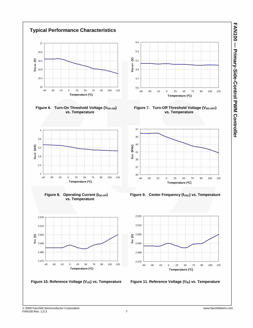
Figure 6. Turn-On Threshold Voltage (VDD-ON) vs. Temperature
Figure 7. Turn-Off Threshold Voltage (VDD-OFF) vs. Temperature
2
2.4
2.8
3.2
3.6
4
-40 -30 -15 0 25 50 75 85 100 125
Temperature (ºC)
IDD-
OP
(mA
)
35
37
39
41
43
45
47
-40 -30 -15 0 25 50 75 85 100 125
Temperature (ºC)
fOSC
(K
Hz)
Figure 8. Operating Current (IDD-OP) vs. Temperature
Figure 9. Center Frequency (fOSC) vs. Temperature
2.475
2.485
2.495
2.505
2.515
2.525
-40 -30 -15 0 25 50 75 85 100 125
Temperature (ºC)
VVR
(V)
2.475
2.485
2.495
2.505
2.515
2.525
-40 -30 -15 0 25 50 75 85 100 125
Temperature (ºC)
VIR
(V)
Figure 10. Reference Voltage (VVR) vs. Temperature Figure 11. Reference Voltage (VIR) vs. Temperature
© 2009 Fairchild Semiconductor Corporation www.fairchildsemi.com FAN100 Rev. 1.0.3 8
FAN
100 — Prim
ary-Side-Control PW
M C
ontroller
Typical Performance Characteristics
500
520
540
560
580
600
-40 -30 -15 0 25 50 75 85 100 125
Temperature (ºC)
fOSC
-N-M
IN (
Hz)
17
18
19
20
21
22
23
-40 -30 -15 0 25 50 75 85 100 125
Temperature (ºC)
fOSC
-CM
-MIN
(K
Hz)
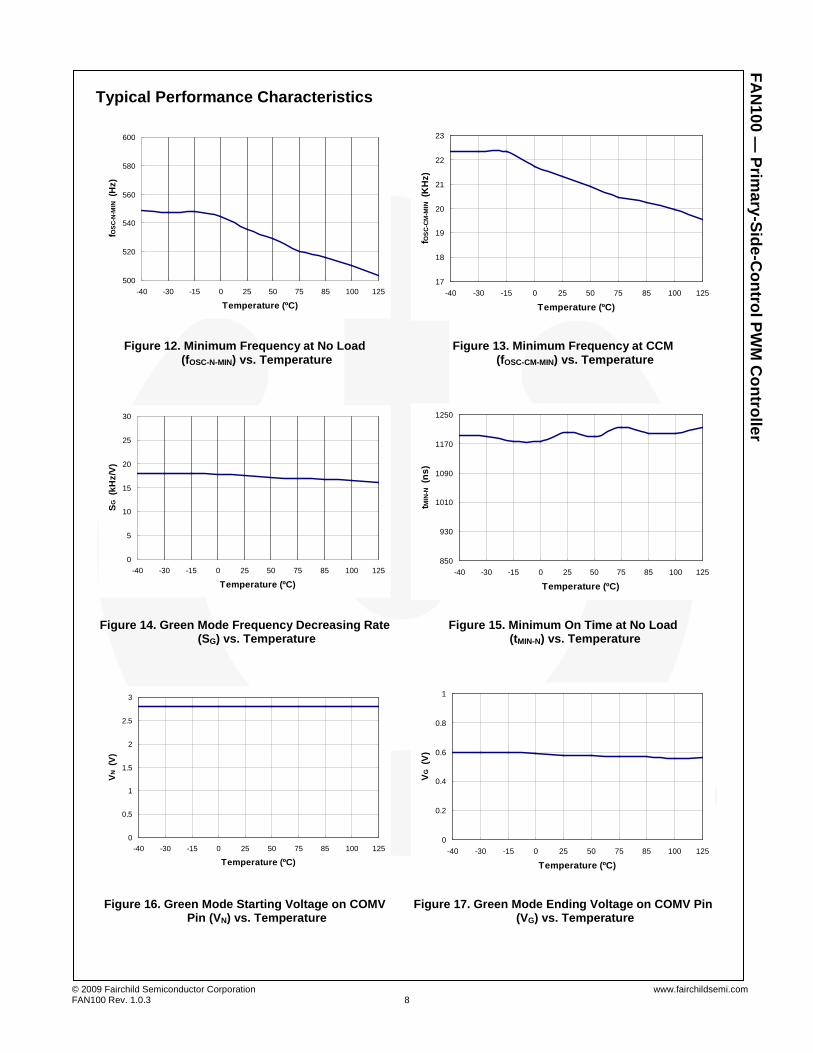
Figure 12. Minimum Frequency at No Load (fOSC-N-MIN) vs. Temperature
Figure 13. Minimum Frequency at CCM (fOSC-CM-MIN) vs. Temperature
0
5
10
15
20
25
30
-40 -30 -15 0 25 50 75 85 100 125
Temperature (ºC)
SG (
kHz/
V)
850
930
1010
1090
1170
1250
-40 -30 -15 0 25 50 75 85 100 125
Temperature (ºC)
tMIN
-N (
ns)
Figure 14. Green Mode Frequency Decreasing Rate (SG) vs. Temperature
Figure 15. Minimum On Time at No Load (tMIN-N) vs. Temperature
0
0.5
1
1.5
2
2.5
3
-40 -30 -15 0 25 50 75 85 100 125
Temperature (ºC)
VN (
V)
0
0.2
0.4
0.6
0.8
1
-40 -30 -15 0 25 50 75 85 100 125
Temperature (ºC)
VG (
V)
Figure 16. Green Mode Starting Voltage on COMV Pin (VN) vs. Temperature
Figure 17. Green Mode Ending Voltage on COMV Pin (VG) vs. Temperature
© 2009 Fairchild Semiconductor Corporation www.fairchildsemi.com FAN100 Rev. 1.0.3 9
FAN
100 — Prim
ary-Side-Control PW
M C
ontroller
Typical Performance Characteristics
74
77
80
83
86
89
92
95
-40 -30 -15 0 25 50 75 85 100 125
Temperature (ºC)
IV-S
INK
(µA
)
75
79
83
87
91
95
-40 -30 -15 0 25 50 75 85 100 125
Temperature (ºC)
IV-S
OUR
CE (
µA)
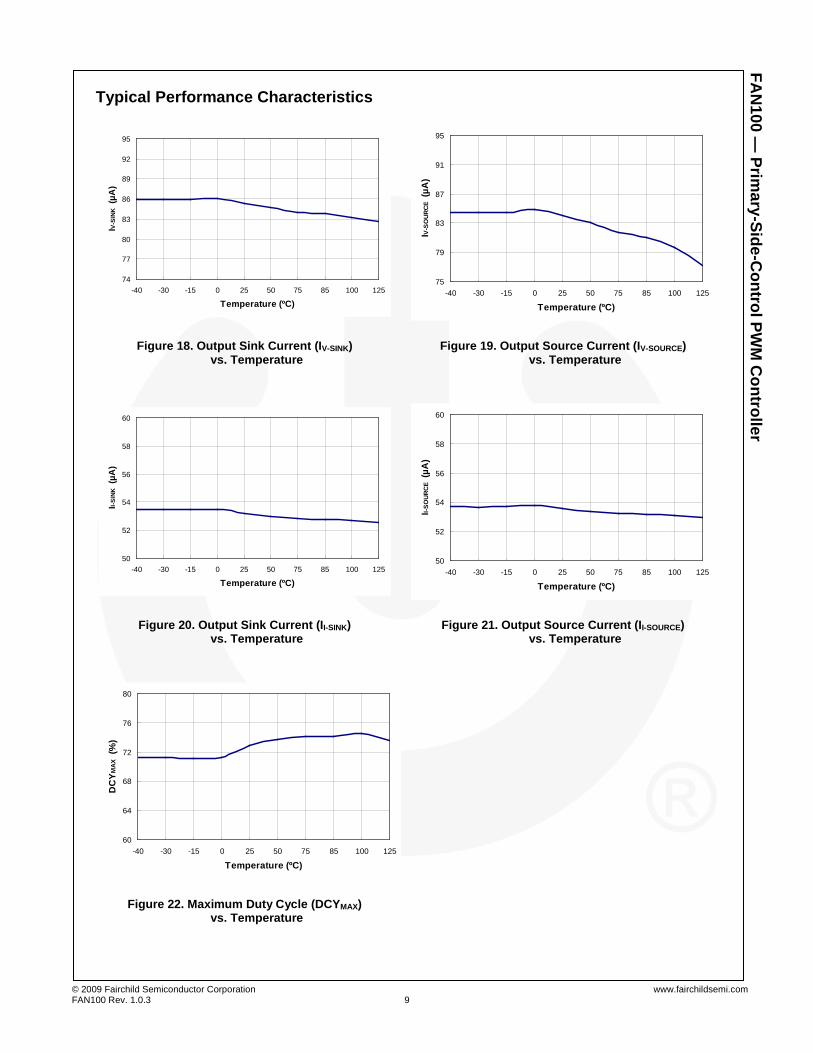
Figure 18. Output Sink Current (IV-SINK) vs. Temperature
Figure 19. Output Source Current (IV-SOURCE) vs. Temperature
50
52
54
56
58
60
-40 -30 -15 0 25 50 75 85 100 125
Temperature (ºC)
II-SIN
K (µ
A)
50
52
54
56
58
60
-40 -30 -15 0 25 50 75 85 100 125
Temperature (ºC)
II-SO
URCE
(µA
)
Figure 20. Output Sink Current (II-SINK) vs. Temperature
Figure 21. Output Source Current (II-SOURCE) vs. Temperature
60
64
68
72
76
80
-40 -30 -15 0 25 50 75 85 100 125
Temperature (ºC)
DC
YMAX
(%
)
Figure 22. Maximum Duty Cycle (DCYMAX) vs. Temperature
© 2009 Fairchild Semiconductor Corporation www.fairchildsemi.com FAN100 Rev. 1.0.3 10
FAN
100 — Prim
ary-Side-Control PW
M C
ontroller
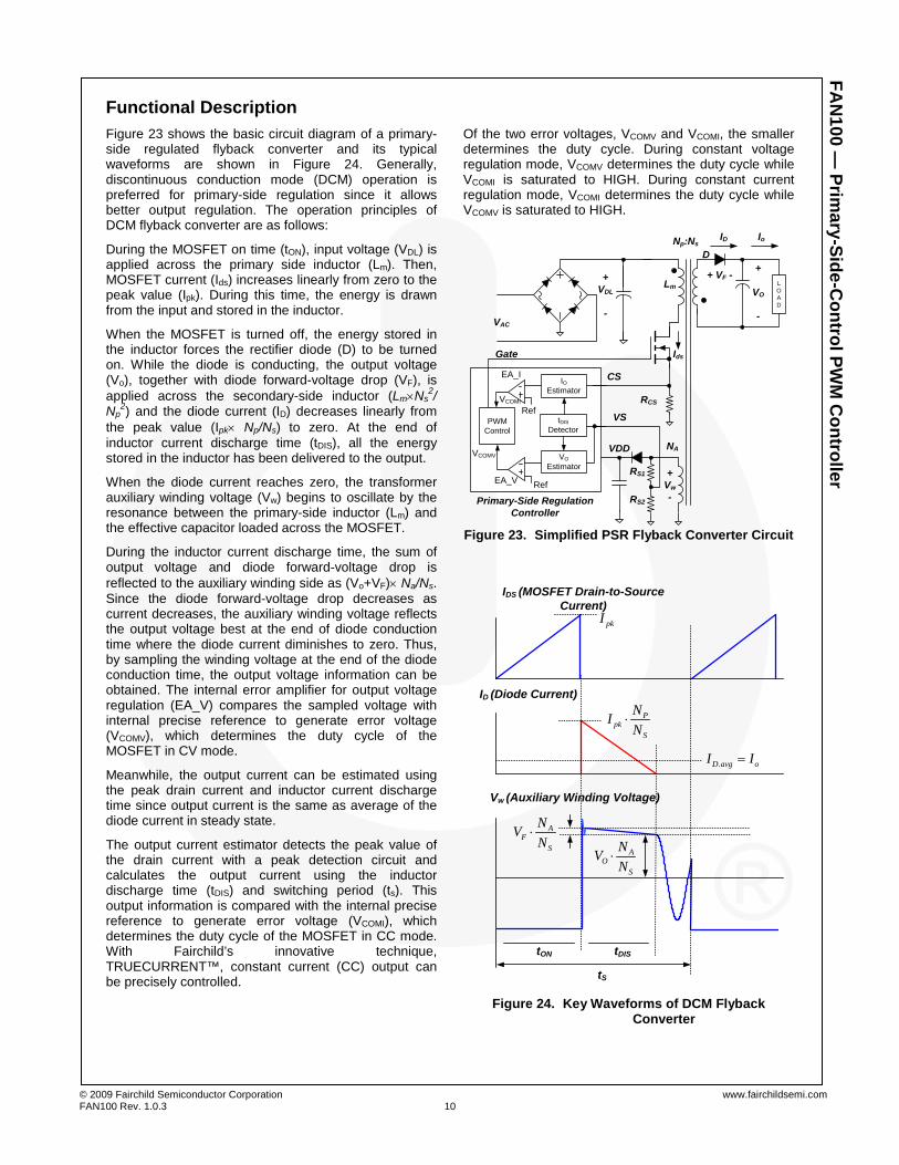
Functional DescriptionFigure 23 shows the basic circuit diagram of a primary-side regulated flyback converter and its typical waveforms are shown in Figure 24. Generally, discontinuous conduction mode (DCM) operation is preferred for primary-side regulation since it allows better output regulation. The operation principles of DCM flyback converter are as follows:
During the MOSFET on time (tON), input voltage (VDL) is applied across the primary side inductor (Lm). Then, MOSFET current (Ids) increases linearly from zero to the peak value (Ipk). During this time, the energy is drawn from the input and stored in the inductor.
When the MOSFET is turned off, the energy stored in the inductor forces the rectifier diode (D) to be turned on. While the diode is conducting, the output voltage (Vo), together with diode forward-voltage drop (VF), is applied across the secondary-side inductor (Lm×Ns
2/ Np
2) and the diode current (ID) decreases linearly from the peak value (Ipk× Np/Ns) to zero. At the end of inductor current discharge time (tDIS), all the energy stored in the inductor has been delivered to the output.
When the diode current reaches zero, the transformer auxiliary winding voltage (Vw) begins to oscillate by the resonance between the primary-side inductor (Lm) and the effective capacitor loaded across the MOSFET.
During the inductor current discharge time, the sum of output voltage and diode forward-voltage drop is reflected to the auxiliary winding side as (Vo+VF)× Na/Ns. Since the diode forward-voltage drop decreases as current decreases, the auxiliary winding voltage reflects the output voltage best at the end of diode conduction time where the diode current diminishes to zero. Thus, by sampling the winding voltage at the end of the diode conduction time, the output voltage information can be obtained. The internal error amplifier for output voltage regulation (EA_V) compares the sampled voltage with internal precise reference to generate error voltage (VCOMV), which determines the duty cycle of the MOSFET in CV mode.
Meanwhile, the output current can be estimated using the peak drain current and inductor current discharge time since output current is the same as average of the diode current in steady state.
The output current estimator detects the peak value of the drain current with a peak detection circuit and calculates the output current using the inductor discharge time (tDIS) and switching period (ts). This output information is compared with the internal precise reference to generate error voltage (VCOMI), which determines the duty cycle of the MOSFET in CC mode. With Fairchild’s innovative technique, TRUECURRENT™, constant current (CC) output can be precisely controlled.
Of the two error voltages, VCOMV and VCOMI, the smaller determines the duty cycle. During constant voltage regulation mode, VCOMV determines the duty cycle while VCOMI is saturated to HIGH. During constant current regulation mode, VCOMI determines the duty cycle while VCOMV is saturated to HIGH.
+VDL
-
Lm
+
VO
-
Np:Ns
Ids
IDD
Primary-Side RegulationController
+Vw-
VDD
Gate
VS
CS
+ VF -
NA
LOAD
Io
IO Estimator
VO Estimator
tDIS Detector
PWM Control
RCS
VAC
Ref
RefEA_V
EA_I
VCOMV
VCOMI
RS1
RS2
Figure 23. Simplified PSR Flyback Converter Circuit
IDS (MOSFET Drain-to-Source Current)
tDIStON
tS
ID (Diode Current)
Vw (Auxiliary Winding Voltage)
Ppk
S
NIN⋅
pkI
.D avg oI I=
AF
S
NVN⋅
AO
S
NVN⋅
Figure 24. Key Waveforms of DCM Flyback
Converter
© 2009 Fairchild Semiconductor Corporation www.fairchildsemi.com FAN100 Rev. 1.0.3 11
FAN
100 — Prim
ary-Side-Control PW
M C
ontroller
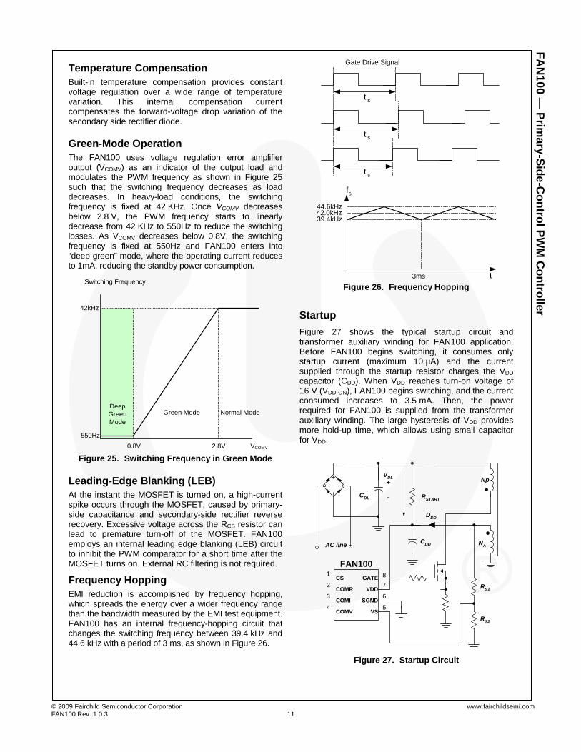
Temperature Compensation Built-in temperature compensation provides constant voltage regulation over a wide range of temperature variation. This internal compensation current compensates the forward-voltage drop variation of the secondary side rectifier diode.
Green-Mode Operation The FAN100 uses voltage regulation error amplifier output (VCOMV) as an indicator of the output load and modulates the PWM frequency as shown in Figure 25 such that the switching frequency decreases as load decreases. In heavy-load conditions, the switching frequency is fixed at 42 KHz. Once VCOMV decreases below 2.8 V, the PWM frequency starts to linearly decrease from 42 KHz to 550Hz to reduce the switching losses. As VCOMV decreases below 0.8V, the switching frequency is fixed at 550Hz and FAN100 enters into “deep green” mode, where the operating current reduces to 1mA, reducing the standby power consumption.
Switching Frequency
42kHz
550HzVCOMV2.8V0.8V
Green Mode Normal ModeDeepGreen Mode
Figure 25. Switching Frequency in Green Mode
Leading-Edge Blanking (LEB) At the instant the MOSFET is turned on, a high-current spike occurs through the MOSFET, caused by primary-side capacitance and secondary-side rectifier reverse recovery. Excessive voltage across the RCS resistor can lead to premature turn-off of the MOSFET. FAN100 employs an internal leading edge blanking (LEB) circuit to inhibit the PWM comparator for a short time after the MOSFET turns on. External RC filtering is not required.
Frequency Hopping EMI reduction is accomplished by frequency hopping, which spreads the energy over a wider frequency range than the bandwidth measured by the EMI test equipment. FAN100 has an internal frequency-hopping circuit that changes the switching frequency between 39.4 kHz and 44.6 kHz with a period of 3 ms, as shown in Figure 26.
t s
t s
t s
Gate Drive Signal
fs
3ms t
44.6kHz
39.4kHz42.0kHz
Figure 26. Frequency Hopping
Startup Figure 27 shows the typical startup circuit and transformer auxiliary winding for FAN100 application. Before FAN100 begins switching, it consumes only startup current (maximum 10 μA) and the current supplied through the startup resistor charges the VDD capacitor (CDD). When VDD reaches turn-on voltage of 16 V (VDD-ON), FAN100 begins switching, and the current consumed increases to 3.5 mA. Then, the power required for FAN100 is supplied from the transformer auxiliary winding. The large hysteresis of VDD provides more hold-up time, which allows using small capacitor for VDD.
NpVDL+
-
AC line
1
NACDD
CDL
CS
COMR
COMI
COMV
GATE
VDD
SGND
VS
RSTART
87
6
5
2
3
4
FAN100
RS1
RS2
DDD
Figure 27. Startup Circuit
© 2009 Fairchild Semiconductor Corporation www.fairchildsemi.com FAN100 Rev. 1.0.3 12
FAN
100 — Prim
ary-Side-Control PW
M C
ontroller
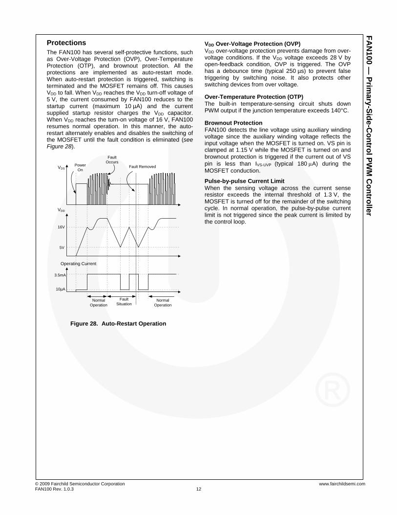
Protections The FAN100 has several self-protective functions, such as Over-Voltage Protection (OVP), Over-Temperature Protection (OTP), and brownout protection. All the protections are implemented as auto-restart mode. When auto-restart protection is triggered, switching is terminated and the MOSFET remains off. This causes VDD to fall. When VDD reaches the VDD turn-off voltage of 5 V, the current consumed by FAN100 reduces to the startup current (maximum 10 µA) and the current supplied startup resistor charges the VDD capacitor. When VDD reaches the turn-on voltage of 16 V, FAN100 resumes normal operation. In this manner, the auto-restart alternately enables and disables the switching of the MOSFET until the fault condition is eliminated (see Figure 28).
Fault Situation
5V
16V
VDD
VDS
Fault Occurs
Fault Removed
Normal Operation
Normal Operation
PowerOn
Operating Current
3.5mA
10µA
Figure 28. Auto-Restart Operation
VDD Over-Voltage Protection (OVP) VDD over-voltage protection prevents damage from over-voltage conditions. If the VDD voltage exceeds 28 V by open-feedback condition, OVP is triggered. The OVP has a debounce time (typical 250 µs) to prevent false triggering by switching noise. It also protects other switching devices from over voltage.
Over-Temperature Protection (OTP) The built-in temperature-sensing circuit shuts down PWM output if the junction temperature exceeds 140°C.
Brownout Protection FAN100 detects the line voltage using auxiliary winding voltage since the auxiliary winding voltage reflects the input voltage when the MOSFET is turned on. VS pin is clamped at 1.15 V while the MOSFET is turned on and brownout protection is triggered if the current out of VS pin is less than IVS-UVP (typical 180 µA) during the MOSFET conduction.
Pulse-by-pulse Current Limit When the sensing voltage across the current sense resistor exceeds the internal threshold of 1.3 V, the MOSFET is turned off for the remainder of the switching cycle. In normal operation, the pulse-by-pulse current limit is not triggered since the peak current is limited by the control loop.
© 2009 Fairchild Semiconductor Corporation www.fairchildsemi.com FAN100 Rev. 1.0.3 13
FAN
100 — Prim
ary-Side-Control PW
M C
ontroller
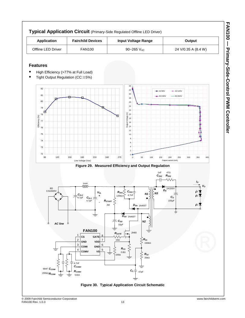
Typical Application Circuit (Primary-Side Regulated Offline LED Driver)
Application Fairchild Devices Input Voltage Range Output
Offline LED Driver FAN100 90~265 VAC 24 V/0.35 A (8.4 W)
Features High Efficiency (>77% at Full Load) Tight Output Regulation (CC:±5%)
81
82
72
73
74
75
76
77
78
79
80
90 120 150 180 210 240 270Line Voltage (Vac)
Effi
cien
cy (%
)
0
2
4
6
8
10
12
14
16
18
20
22
24
26
28
30
32
34
0 50 100 150 200 250 300 350 400Output current (mA)
Out
put V
olta
ge (V
)
AC90V AC120V
AC230V AC264V
Figure 29. Measured Efficiency and Output Regulation
N1 N3RSN1 CSN1VDL+
-
AC line
DSN
DR
CO
1
N2CDD
VO
CDL1
CS
GND
COMI
COMV
GATE
VDD
GND
VS
RSTART
RSN2CSN2
87
6
5
2
3
4
FAN100
IO
RS1
RS2
CS
RGATE
RCS
RCOMV
CCOMV
RCOMI
CCOMI
120kΩ 4.7nF
2M 1N4007
150kΩ
20kΩ
0.8Ω
10Ω
10µF
47pF
4.7µF
BD 0.5A/600V
4.7µFCDL2
1mH
4.7nF
51kΩ
68nF
200kΩ
1nF 47Ω
220µF
DDD 1N4007
100Ω
2A/200V
2N60
Figure 30. Typical Application Circuit Schematic
© 2009 Fairchild Semiconductor Corporation www.fairchildsemi.com FAN100 Rev. 1.0.3 14
FAN
100 — Prim
ary-Side-Control PW
M C
ontroller
Typical Application Circuit (Continued)
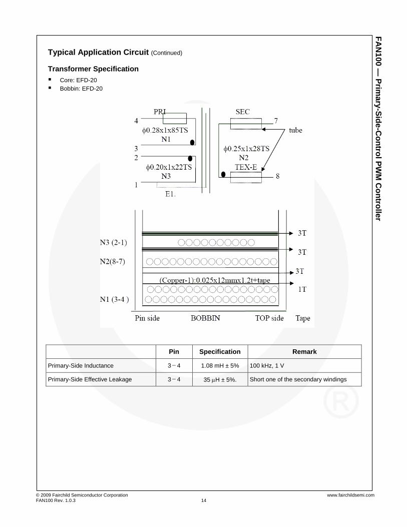
Transformer Specification Core: EFD-20 Bobbin: EFD-20
Pin Specification Remark
Primary-Side Inductance 3-4 1.08 mH ± 5% 100 kHz, 1 V
Primary-Side Effective Leakage 3-4 35 µH ± 5%. Short one of the secondary windings
© 2009 Fairchild Semiconductor Corporation www.fairchildsemi.com FAN100 Rev. 1.0.3 15
FAN
100 — Prim
ary-Side-Control PW
M C
ontroller
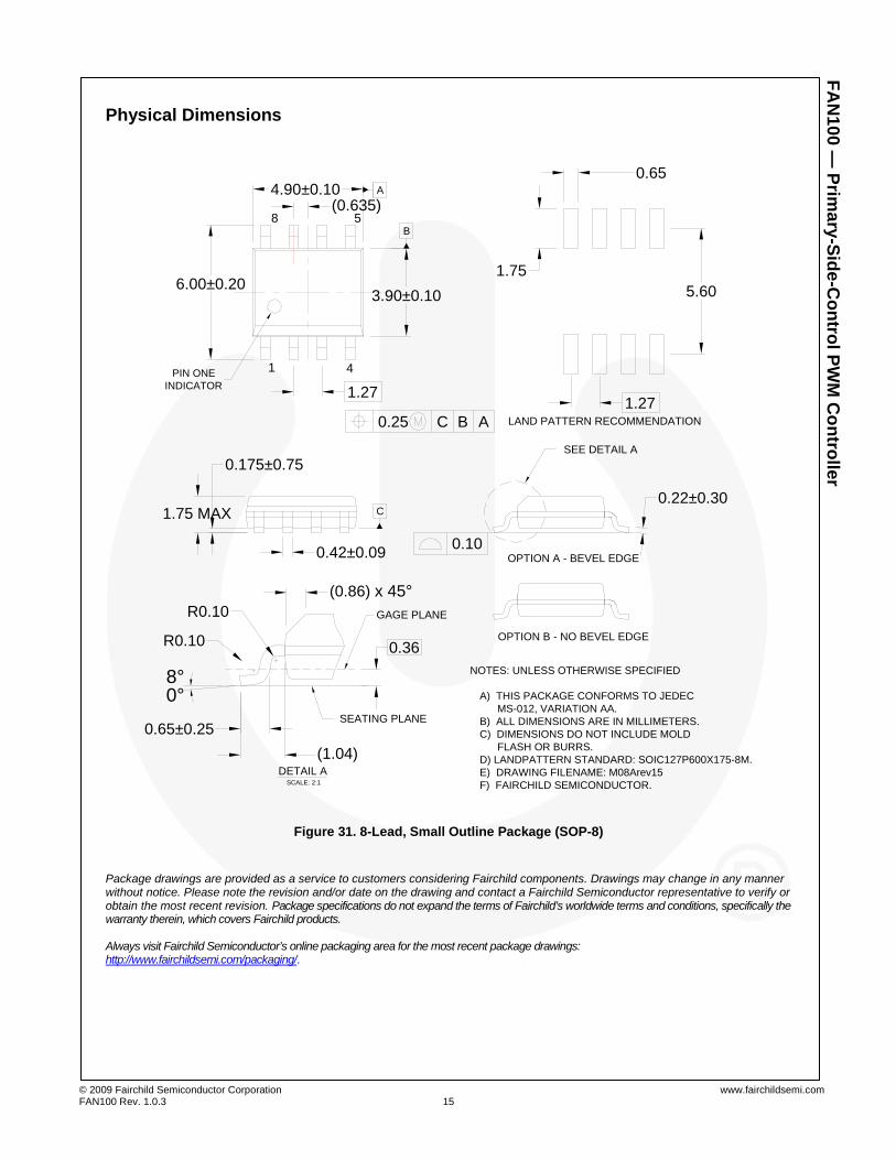
Physical Dimensions
8°0°
SEE DETAIL A
NOTES: UNLESS OTHERWISE SPECIFIED
A) THIS PACKAGE CONFORMS TO JEDEC MS-012, VARIATION AA. B) ALL DIMENSIONS ARE IN MILLIMETERS. C) DIMENSIONS DO NOT INCLUDE MOLD FLASH OR BURRS. D) LANDPATTERN STANDARD: SOIC127P600X175-8M. E) DRAWING FILENAME: M08Arev15 F) FAIRCHILD SEMICONDUCTOR.
LAND PATTERN RECOMMENDATION
SEATING PLANE
C
GAGE PLANE
x 45°
DETAIL ASCALE: 2:1
PIN ONEINDICATOR
4
8
1
B5
A
5.60
0.65
1.75
1.27
6.00±0.203.90±0.10
4.90±0.10
1.27
0.42±0.09
0.175±0.75
1.75 MAX
0.36
(0.86)R0.10
R0.10
0.65±0.25(1.04)
OPTION A - BEVEL EDGE
OPTION B - NO BEVEL EDGE
0.25 C B A
0.10
0.22±0.30
(0.635)
Figure 31. 8-Lead, Small Outline Package (SOP-8)
Package drawings are provided as a service to customers considering Fairchild components. Drawings may change in any manner without notice. Please note the revision and/or date on the drawing and contact a Fairchild Semiconductor representative to verify or obtain the most recent revision. Package specifications do not expand the terms of Fairchild’s worldwide terms and conditions, specifically the warranty therein, which covers Fairchild products. Always visit Fairchild Semiconductor’s online packaging area for the most recent package drawings: http://www.fairchildsemi.com/packaging/.
© 2009 Fairchild Semiconductor Corporation www.fairchildsemi.com FAN100 Rev. 1.0.3 16
FAN
100 — Prim
ary-Side-Control PW
M C
ontroller