HIGH-SPEED PWM CONTROLLER - TI.com
19
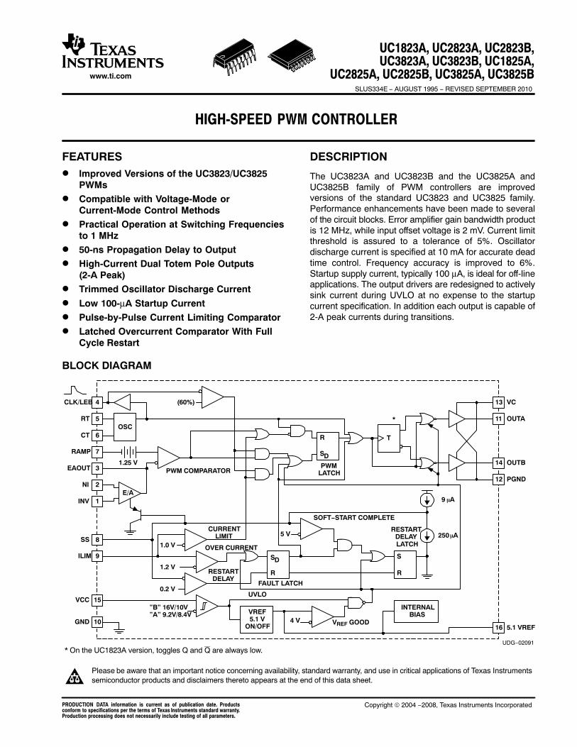
UC1823A, UC2823A, UC2823B, UC3823A, UC3823B, UC1825A, UC2825A, UC2825B, UC3825A, UC3825B SLUS334E − AUGUST 1995 − REVISED SEPTEMBER 2010 HIGH-SPEED PWM CONTROLLER FEATURES D Improved Versions of the UC3823/UC3825 PWMs D Compatible with Voltage-Mode or Current-Mode Control Methods D Practical Operation at Switching Frequencies to 1 MHz D 50-ns Propagation Delay to Output D High-Current Dual Totem Pole Outputs (2-A Peak) D Trimmed Oscillator Discharge Current D Low 100-μA Startup Current D Pulse-by-Pulse Current Limiting Comparator D Latched Overcurrent Comparator With Full Cycle Restart DESCRIPTION The UC3823A and UC3823B and the UC3825A and UC3825B family of PWM controllers are improved versions of the standard UC3823 and UC3825 family. Performance enhancements have been made to several of the circuit blocks. Error amplifier gain bandwidth product is 12 MHz, while input offset voltage is 2 mV. Current limit threshold is assured to a tolerance of 5%. Oscillator discharge current is specified at 10 mA for accurate dead time control. Frequency accuracy is improved to 6%. Startup supply current, typically 100 μA, is ideal for off-line applications. The output drivers are redesigned to actively sink current during UVLO at no expense to the startup current specification. In addition each output is capable of 2-A peak currents during transitions. BLOCK DIAGRAM 4 5 6 7 3 2 1 OSC CLK/LEB RT CT RAMP EAOUT NI INV 8 9 15 SS ILIM VCC 1.25 V 10 GND (60%) 1.0 V E/A 1.2 V 0.2 V OVER CURRENT CURRENT LIMIT R S D 5 V SOFT−START COMPLETE R S D FAULT LATCH RESTART DELAY T 13 11 14 VC 12 PWM LATCH 9 mA 250 mA R S * RESTART DELAY LATCH VREF 5.1 V ON/OFF UVLO 4 V INTERNAL BIAS 16 OUTA OUTB PGND 5.1 VREF ”B” 16V/10V ”A” 9.2V/8.4V PWM COMPARATOR UDG−02091 V REF GOOD * On the UC1823A version, toggles Q and Q are always low. Please be aware that an important notice concerning availability, standard warranty, and use in critical applications of Texas Instruments semiconductor products and disclaimers thereto appears at the end of this data sheet. www.ti.com Copyright © 2004 −2008, Texas Instruments Incorporated PRODUCTION DATA information is current as of publication date. Products conform to specifications per the terms of Texas Instruments standard warranty. Production processing does not necessarily include testing of all parameters.
Transcript of HIGH-SPEED PWM CONTROLLER - TI.com
UC1823A, UC2823A, UC2823B,UC3823A, UC3823B, UC1825A,
UC2825A, UC2825B, UC3825A, UC3825BSLUS334E − AUGUST 1995 − REVISED SEPTEMBER 2010
HIGH-SPEED PWM CONTROLLER
FEATURES� Improved Versions of the UC3823/UC3825
PWMs
� Compatible with Voltage-Mode orCurrent-Mode Control Methods
� Practical Operation at Switching Frequenciesto 1 MHz
� 50-ns Propagation Delay to Output
� High-Current Dual Totem Pole Outputs(2-A Peak)
� Trimmed Oscillator Discharge Current
� Low 100-μA Startup Current
� Pulse-by-Pulse Current Limiting Comparator
� Latched Overcurrent Comparator With FullCycle Restart
DESCRIPTION
The UC3823A and UC3823B and the UC3825A andUC3825B family of PWM controllers are improvedversions of the standard UC3823 and UC3825 family.Performance enhancements have been made to severalof the circuit blocks. Error amplifier gain bandwidth productis 12 MHz, while input offset voltage is 2 mV. Current limitthreshold is assured to a tolerance of 5%. Oscillatordischarge current is specified at 10 mA for accurate deadtime control. Frequency accuracy is improved to 6%.Startup supply current, typically 100 μA, is ideal for off-lineapplications. The output drivers are redesigned to activelysink current during UVLO at no expense to the startupcurrent specification. In addition each output is capable of2-A peak currents during transitions.
BLOCK DIAGRAM
4
5
6
7
3
2
1
OSC
CLK/LEB
RT
CT
RAMP
EAOUT
NI
INV
8
9
15
SS
ILIM
VCC
1.25 V
10GND
(60%)
1.0 V
E/A
1.2 V
0.2 V
OVER CURRENT
CURRENTLIMIT
R
SD
5 V
SOFT−START COMPLETE
R
SD
FAULT LATCH
RESTARTDELAY
T
13
11
14
VC
12
PWMLATCH
9 �A
250�A
R
S
*
RESTARTDELAY LATCH
VREF5.1 V
ON/OFF
UVLO
4 V
INTERNALBIAS
16
OUTA
OUTB
PGND
5.1 VREF
”B” 16V/10V”A” 9.2V/8.4V
PWM COMPARATOR
UDG−02091
VREF GOOD
* On the UC1823A version, toggles Q and Q are always low.
Please be aware that an important notice concerning availability, standard warranty, and use in critical applications of Texas Instrumentssemiconductor products and disclaimers thereto appears at the end of this data sheet.
www.ti.com
Copyright © 2004 −2008, Texas Instruments IncorporatedPRODUCTION DATA information is current as of publication date. Productsconform to specifications per the terms of Texas Instruments standard warranty.Production processing does not necessarily include testing of all parameters.
UC1823A, UC2823A, UC2823B,UC3823A, UC3823B, UC1825A,UC2825A, UC2825B, UC3825A, UC3825BSLUS334E − AUGUST 1995 − REVISED SEPTEMBER 2010
www.ti.com
2
These devices have limited built-in ESD protection. The leads should be shorted together or the device placed in conductive foam duringstorage or handling to prevent electrostatic damage to the MOS gates.
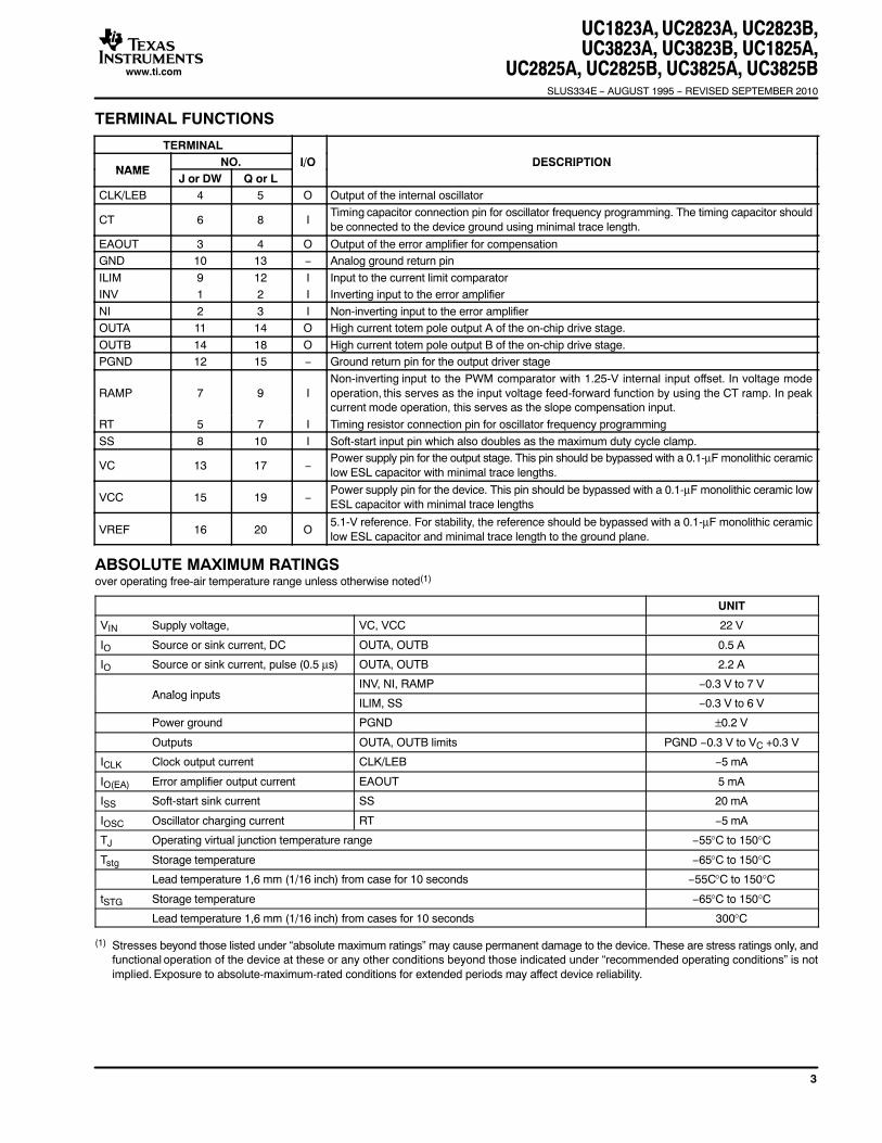
DESCRIPTION (CONTINUED)Functional improvements have also been implemented in this family. The UC3825 shutdown comparator is now ahigh-speed overcurrent comparator with a threshold of 1.2 V. The overcurrent comparator sets a latch that ensures fulldischarge of the soft-start capacitor before allowing a restart. While the fault latch is set, the outputs are in the low state.In the event of continuous faults, the soft-start capacitor is fully charged before discharge to insure that the fault frequencydoes not exceed the designed soft start period. The UC3825 CLOCK pin has become CLK/LEB. This pin combines thefunctions of clock output and leading edge blanking adjustment and has been buffered for easier interfacing.
The UC3825A and UC3825B have dual alternating outputs and the same pin configuration of the UC3825. The UC3823Aand UC3823B outputs operate in phase with duty cycles from zero to less than 100%. The pin configuration of the UC3823Aand UC3823B is the same as the UC3823 except pin 11 is now an output pin instead of the reference pin to the currentlimit comparator. “A” version parts have UVLO thresholds identical to the original UC3823 and UC3825. The “B” versionshave UVLO thresholds of 16 V and 10 V, intended for ease of use in off-line applications.
Consult the application note, The UC3823A,B and UC3825A,B Enhanced Generation of PWM Controllers, (SLUA125) fordetailed technical and applications information.
ORDERING INFORMATIONUVLO
TAMAXIMUM 9.2 V / 8.4 V 16 V / 10 V
TAMAXIMUM
DUTY CYCLE SOIC−16(1)
(DW)PDIP−16
(N)PLCC−20(1)
(Q)SOIC−16
(DW)PDIP−16
(N)PLCC−20(1)
(Q)
40°C to 85°C< 100% UC2823ADW UC2823AN UC2823AQ UC2823BDW UC2823BN −
−40°C to 85°C< 50% UC2825ADW UC2825AN UC2825AQ UC2825BDW UC2825BN −
0°C to 70°C< 100% UC3823ADW UC3823AN UC3823AQ UC3823BDW UC3823BN −
−0°C to 70°C< 50% UC3825ADW UC3825AN UC3825AQ UC3825BDW UC3825BN UC3825BQ
(1) The DW and Q packages are also available taped and reeled. Add TR suffix to the device type (i.e., UC2823ADWR). To order quantities of 1000devices per reel for the Q package and 2000 devices per reel for the DW package.
UVLO
TAMAXIMUM 9.2 V / 8.4 V
TAMAXIMUM
DUTY CYCLE CDIP−16(J)
LCCC−20(L)
55°C to 125°C< 100% UC1823AJ, UC1823AJ883B, UC1823AJQMLV UC1823AL, UC1823AL883B
−55°C to 125°C< 50% UC1825AJ, UC1825AJ883B, UC1825AJQMLV UC1825AL, UC1825AL883B, UC1825ALQMLV
PIN ASSIGNMENTS
1
2
3
4
5
6
7
8
16
15
14
13
12
11
10
9
INVNI
EAOUTCLK/LEB
RTCT
RAMPSS
VREFVCCOUTBVCPGNDOUTAGNDILIM
DW, J, OR N PACKAGES(TOP VIEW)
3 2 1 20 19
9 10 11 12 13
4
5
6
7
8
18
17
16
15
14
OUTBVCNCPGNDOUTA
EAOUTCLK/LEB
NCRTCT
Q OR L PACKAGES(TOP VIEW)
NI
INV
NC
ILIM
GN
DV
RE
FV
CC
RA
MP
SS
NC
NC = no connection
UC1823A, UC2823A, UC2823B,UC3823A, UC3823B, UC1825A,
UC2825A, UC2825B, UC3825A, UC3825BSLUS334E − AUGUST 1995 − REVISED SEPTEMBER 2010
www.ti.com
3
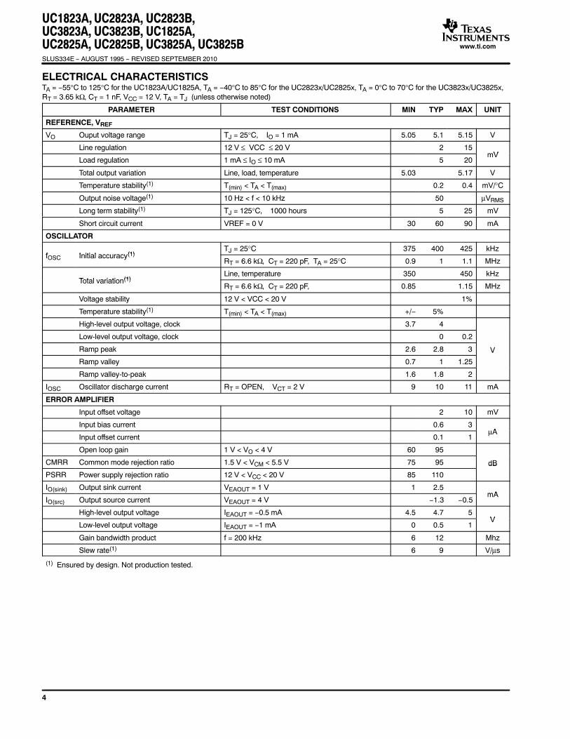
TERMINAL FUNCTIONS
TERMINAL
NAMENO. I/O DESCRIPTION
NAMEJ or DW Q or L
I/O DESCRIPTION
CLK/LEB 4 5 O Output of the internal oscillator
CT 6 8 ITiming capacitor connection pin for oscillator frequency programming. The timing capacitor shouldbe connected to the device ground using minimal trace length.
EAOUT 3 4 O Output of the error amplifier for compensationGND 10 13 − Analog ground return pin
ILIM 9 12 I Input to the current limit comparatorINV 1 2 I Inverting input to the error amplifier
NI 2 3 I Non-inverting input to the error amplifierOUTA 11 14 O High current totem pole output A of the on-chip drive stage.
OUTB 14 18 O High current totem pole output B of the on-chip drive stage.PGND 12 15 − Ground return pin for the output driver stage
RAMP 7 9 INon-inverting input to the PWM comparator with 1.25-V internal input offset. In voltage modeoperation, this serves as the input voltage feed-forward function by using the CT ramp. In peakcurrent mode operation, this serves as the slope compensation input.
RT 5 7 I Timing resistor connection pin for oscillator frequency programming
SS 8 10 I Soft-start input pin which also doubles as the maximum duty cycle clamp.
VC 13 17 −Power supply pin for the output stage. This pin should be bypassed with a 0.1-μF monolithic ceramiclow ESL capacitor with minimal trace lengths.
VCC 15 19 −Power supply pin for the device. This pin should be bypassed with a 0.1-μF monolithic ceramic lowESL capacitor with minimal trace lengths
VREF 16 20 O5.1-V reference. For stability, the reference should be bypassed with a 0.1-μF monolithic ceramiclow ESL capacitor and minimal trace length to the ground plane.
ABSOLUTE MAXIMUM RATINGSover operating free-air temperature range unless otherwise noted(1)
UNIT
VIN Supply voltage, VC, VCC 22 V
IO Source or sink current, DC OUTA, OUTB 0.5 A
IO Source or sink current, pulse (0.5 μs) OUTA, OUTB 2.2 A
Analog inputsINV, NI, RAMP −0.3 V to 7 V
Analog inputsILIM, SS −0.3 V to 6 V
Power ground PGND ±0.2 V
Outputs OUTA, OUTB limits PGND −0.3 V to VC +0.3 V
ICLK Clock output current CLK/LEB −5 mA
IO(EA) Error amplifier output current EAOUT 5 mA
ISS Soft-start sink current SS 20 mA
IOSC Oscillator charging current RT −5 mA
TJ Operating virtual junction temperature range −55°C to 150°C
Tstg Storage temperature −65°C to 150°C
Lead temperature 1,6 mm (1/16 inch) from case for 10 seconds −55C°C to 150°C
tSTG Storage temperature −65°C to 150°C
Lead temperature 1,6 mm (1/16 inch) from cases for 10 seconds 300°C
(1) Stresses beyond those listed under “absolute maximum ratings” may cause permanent damage to the device. These are stress ratings only, andfunctional operation of the device at these or any other conditions beyond those indicated under “recommended operating conditions” is notimplied. Exposure to absolute-maximum-rated conditions for extended periods may affect device reliability.
UC1823A, UC2823A, UC2823B,UC3823A, UC3823B, UC1825A,UC2825A, UC2825B, UC3825A, UC3825BSLUS334E − AUGUST 1995 − REVISED SEPTEMBER 2010
www.ti.com
4
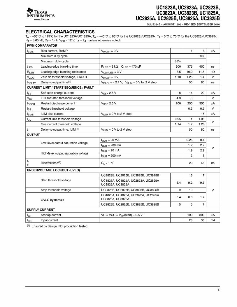
ELECTRICAL CHARACTERISTICSTA = −55°C to 125°C for the UC1823A/UC1825A, TA = −40°C to 85°C for the UC2823x/UC2825x, TA = 0°C to 70°C for the UC3823x/UC3825x,RT = 3.65 kΩ, CT = 1 nF, VCC = 12 V, TA = TJ (unless otherwise noted)
PARAMETER TEST CONDITIONS MIN TYP MAX UNIT
REFERENCE, VREF
VO Ouput voltage range TJ = 25°C, IO = 1 mA 5.05 5.1 5.15 V
Line regulation 12 V ≤ VCC ≤ 20 V 2 15mV
Load regulation 1 mA ≤ IO ≤ 10 mA 5 20mV
Total output variation Line, load, temperature 5.03 5.17 V
Temperature stability(1) T(min) < TA < T(max) 0.2 0.4 mV/°C
Output noise voltage(1) 10 Hz < f < 10 kHz 50 μVRMS
Long term stability(1) TJ = 125°C, 1000 hours 5 25 mV
Short circuit current VREF = 0 V 30 60 90 mA
OSCILLATOR
f Initial accuracy(1)TJ = 25°C 375 400 425 kHz
fOSC Initial accuracy(1)RT = 6.6 kΩ, CT = 220 pF, TA = 25°C 0.9 1 1.1 MHz
Total variation(1)Line, temperature 350 450 kHz
Total variation(1)RT = 6.6 kΩ, CT = 220 pF, 0.85 1.15 MHz
Voltage stability 12 V < VCC < 20 V 1%
Temperature stability(1) T(min) < TA < T(max) +/− 5%
High-level output voltage, clock 3.7 4
Low-level output voltage, clock 0 0.2
Ramp peak 2.6 2.8 3 V
Ramp valley 0.7 1 1.25
V
Ramp valley-to-peak 1.6 1.8 2
IOSC Oscillator discharge current RT = OPEN, VCT = 2 V 9 10 11 mA
ERROR AMPLIFIER
Input offset voltage 2 10 mV
Input bias current 0.6 3A
Input offset current 0.1 1μA
Open loop gain 1 V < VO < 4 V 60 95
CMRR Common mode rejection ratio 1.5 V < VCM < 5.5 V 75 95 dB
PSRR Power supply rejection ratio 12 V < VCC < 20 V 85 110
dB
IO(sink) Output sink current VEAOUT = 1 V 1 2.5mA
IO(src) Output source current VEAOUT = 4 V −1.3 −0.5mA
High-level output voltage IEAOUT = −0.5 mA 4.5 4.7 5V
Low-level output voltage IEAOUT = −1 mA 0 0.5 1V
Gain bandwidth product f = 200 kHz 6 12 Mhz
Slew rate(1) 6 9 V/μs
(1) Ensured by design. Not production tested.
UC1823A, UC2823A, UC2823B,UC3823A, UC3823B, UC1825A,
UC2825A, UC2825B, UC3825A, UC3825BSLUS334E − AUGUST 1995 − REVISED SEPTEMBER 2010
www.ti.com
5
ELECTRICAL CHARACTERISTICSTA = −55°C to 125°C for the UC1823A/UC1825A, TA = −40°C to 85°C for the UC2823x/UC2825x, TA = 0°C to 70°C for the UC3823x/UC3825x,RT = 3.65 kΩ, CT = 1 nF, VCC = 12 V, TA = TJ (unless otherwise noted)
PWM COMPARATOR
IBIAS Bias current, RAMP VRAMP = 0 V −1 −8 μA
Minimum duty cycle 0%
Maximum duty cycle 85%
tLEB Leading edge blanking time RLEB = 2 kΩ, CLEB = 470 pF 300 375 450 ns
RLEB Leading edge blanking resistance VCLK/LEB = 3 V 8.5 10.0 11.5 kΩ
VZDC Zero dc threshold voltage, EAOUT VRAMP = 0 V 1.10 1.25 1.4 V
tDELAY Delay-to-output time(1) VEAOUT = 2.1 V, VILIM = 0 V to 2 V step 50 80 ns
CURRENT LIMIT / START SEQUENCE / FAULT
ISS Soft-start charge current VSS= 2.5 V 8 14 20 μA
VSS Full soft-start threshold voltage 4.3 5 V
IDSCH Restart discharge current VSS= 2.5 V 100 250 350 μA
ISS Restart threshold voltage 0.3 0.5 V
IBIAS ILIM bias current VILIM = 0 V to 2 V step 15 μA
ICL Current limit threshold voltage 0.95 1 1.05V
Overcurrent threshold voltage 1.14 1.2 1.26V
td Delay-to-output time, ILIM(1) VILIM = 0 V to 2 V step 50 80 ns
OUTPUT
Low level output saturation voltageIOUT = 20 mA 0.25 0.4
Low-level output saturation voltageIOUT = 200 mA 1.2 2.2
V
High level output saturation voltageIOUT = 20 mA 1.9 2.9
V
High-level output saturation voltageIOUT = 200 mA 2 3
tr,tf
Rise/fall time(1) CL = 1 nF 20 45 ns
UNDERVOLTAGE LOCKOUT (UVLO)
UC2823B, UC2825B, UC3825B, UC3825B 16 17
Start threshold voltage UC1823A, UC1825A, UC2823A, UC2825AUC3825A, UC3825A
8.4 9.2 9.6
Stop threshold voltage UC2823B, UC2825B, UC3825B, UC3825B 9 10 V
OVLO hysteresis
UC1823A, UC1825A, UC2823A, UC2825AUC3825A, UC3825A
0.4 0.8 1.2
V
OVLO hysteresisUC2823B, UC2825B, UC3825B, UC3825B 5 6 7
SUPPLY CURRENT
Isu Startup current VC = VCC = VTH(start) − 0.5 V 100 300 μA
ICC Input current 28 36 mA
(1) Ensured by design. Not production tested.
UC1823A, UC2823A, UC2823B,UC3823A, UC3823B, UC1825A,UC2825A, UC2825B, UC3825A, UC3825BSLUS334E − AUGUST 1995 − REVISED SEPTEMBER 2010
www.ti.com
6
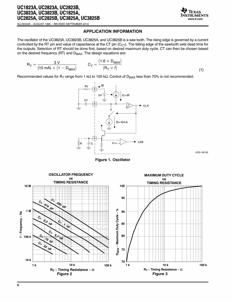
APPLICATION INFORMATION
The oscillator of the UC3823A, UC3823B, UC3825A, and UC3825B is a saw tooth. The rising edge is governed by a currentcontrolled by the RT pin and value of capacitance at the CT pin (CCT). The falling edge of the sawtooth sets dead time forthe outputs. Selection of RT should be done first, based on desired maximum duty cycle. CT can then be chosen basedon the desired frequency (RT) and DMAX. The design equations are:
RT � 3 V(10 mA) � �1 � DMAX
� CT ��1.6 � DMAX
��RT � f�
Recommended values for RT range from 1 kΩ to 100 kΩ. Control of DMAX less than 70% is not recommended.
UDG−95102
Figure 1. Oscillator
10 M
1 M
100 k
10 k
1 k 10 k 100 k
Figure 2RT − Timing Resistance − �
OSCILLATOR FREQUENCYvs
TIMING RESISTANCE
f − F
req
uen
cy −
Hz
Figure 3
1 k 10 k70
75
80
85
90
95
100
100 k
DM
AX
− M
axim
um
Du
ty C
ycle
− %
RT − Timing Resistance − �
MAXIMUM DUTY CYCLEvs
TIMING RESISTANCE
(1)
UC1823A, UC2823A, UC2823B,UC3823A, UC3823B, UC1825A,
UC2825A, UC2825B, UC3825A, UC3825BSLUS334E − AUGUST 1995 − REVISED SEPTEMBER 2010
www.ti.com
7
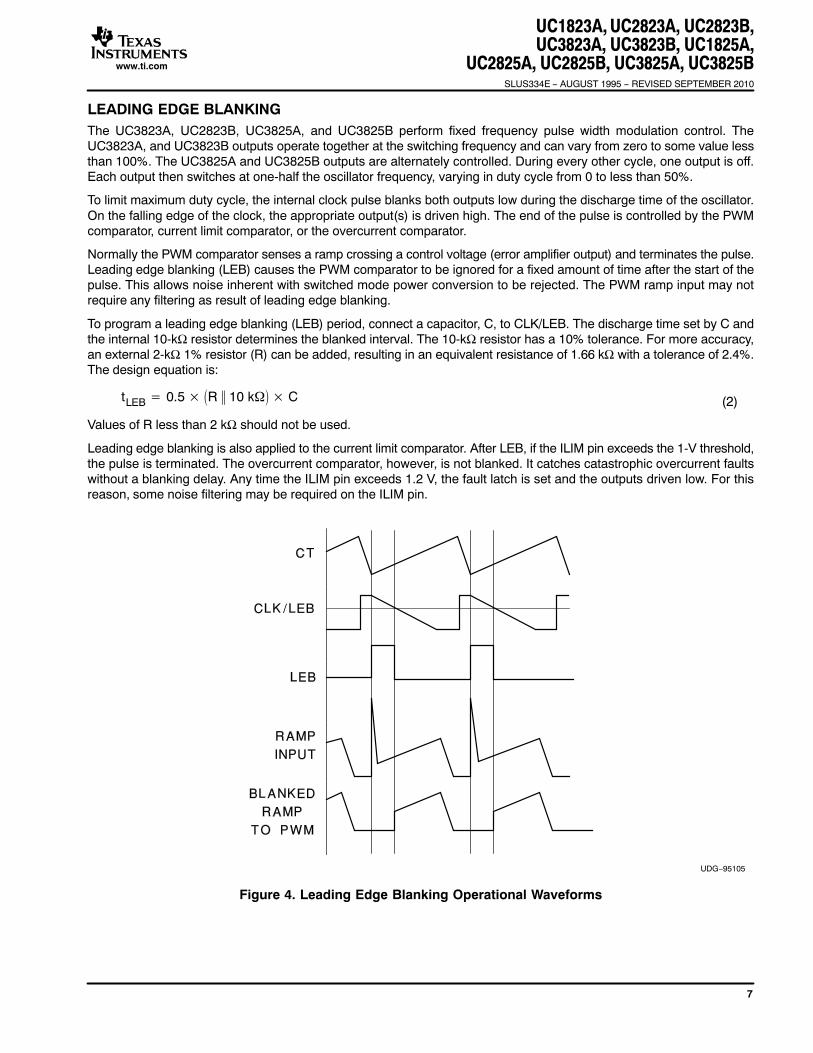
LEADING EDGE BLANKINGThe UC3823A, UC2823B, UC3825A, and UC3825B perform fixed frequency pulse width modulation control. TheUC3823A, and UC3823B outputs operate together at the switching frequency and can vary from zero to some value lessthan 100%. The UC3825A and UC3825B outputs are alternately controlled. During every other cycle, one output is off.Each output then switches at one-half the oscillator frequency, varying in duty cycle from 0 to less than 50%.
To limit maximum duty cycle, the internal clock pulse blanks both outputs low during the discharge time of the oscillator.On the falling edge of the clock, the appropriate output(s) is driven high. The end of the pulse is controlled by the PWMcomparator, current limit comparator, or the overcurrent comparator.
Normally the PWM comparator senses a ramp crossing a control voltage (error amplifier output) and terminates the pulse.Leading edge blanking (LEB) causes the PWM comparator to be ignored for a fixed amount of time after the start of thepulse. This allows noise inherent with switched mode power conversion to be rejected. The PWM ramp input may notrequire any filtering as result of leading edge blanking.
To program a leading edge blanking (LEB) period, connect a capacitor, C, to CLK/LEB. The discharge time set by C andthe internal 10-kΩ resistor determines the blanked interval. The 10-kΩ resistor has a 10% tolerance. For more accuracy,an external 2-kΩ 1% resistor (R) can be added, resulting in an equivalent resistance of 1.66 kΩ with a tolerance of 2.4%.The design equation is:
tLEB � 0.5 � �R � 10 k�� � C
Values of R less than 2 kΩ should not be used.
Leading edge blanking is also applied to the current limit comparator. After LEB, if the ILIM pin exceeds the 1-V threshold,the pulse is terminated. The overcurrent comparator, however, is not blanked. It catches catastrophic overcurrent faultswithout a blanking delay. Any time the ILIM pin exceeds 1.2 V, the fault latch is set and the outputs driven low. For thisreason, some noise filtering may be required on the ILIM pin.
UDG−95105
Figure 4. Leading Edge Blanking Operational Waveforms
(2)
UC1823A, UC2823A, UC2823B,UC3823A, UC3823B, UC1825A,UC2825A, UC2825B, UC3825A, UC3825BSLUS334E − AUGUST 1995 − REVISED SEPTEMBER 2010
www.ti.com
8
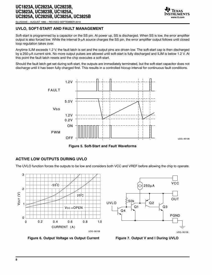
UVLO, SOFT-START AND FAULT MANAGEMENT
Soft-start is programmed by a capacitor on the SS pin. At power up, SS is discharged. When SS is low, the error amplifieroutput is also forced low. While the internal 9-μA source charges the SS pin, the error amplifier output follows until closedloop regulation takes over.
Anytime ILIM exceeds 1.2 V, the fault latch is set and the output pins are driven low. The soft-start cap is then dischargedby a 250-μA current sink. No more output pulses are allowed until soft-start is fully discharged and ILIM is below 1.2 V. Atthis point the fault latch resets and the chip executes a soft-start.
Should the fault latch get set during soft-start, the outputs are immediately terminated, but the soft-start capacitor does notdischarge until it has been fully charged first. This results in a controlled hiccup interval for continuous fault conditions.
UDG−95106
Figure 5. Soft-Start and Fault Waveforms
ACTIVE LOW OUTPUTS DURING UVLO
The UVLO function forces the outputs to be low and considers both VCC and VREF before allowing the chip to operate.
Figure 6. Output Voltage vs Output Current
UDG−95108 UDG−95106
Figure 7. Output V and I During UVLO
UC1823A, UC2823A, UC2823B,UC3823A, UC3823B, UC1825A,
UC2825A, UC2825B, UC3825A, UC3825BSLUS334E − AUGUST 1995 − REVISED SEPTEMBER 2010
www.ti.com
9
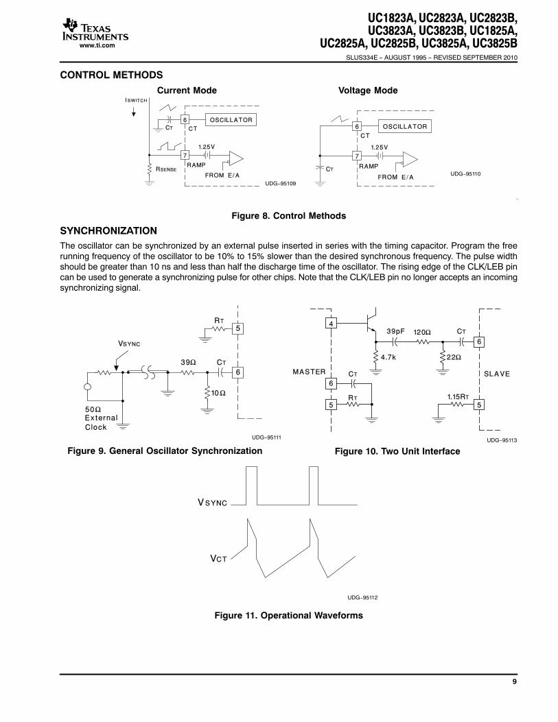
CONTROL METHODS
UDG−95109
UDG−95110
Current Mode Voltage Mode
.
Figure 8. Control Methods
SYNCHRONIZATIONThe oscillator can be synchronized by an external pulse inserted in series with the timing capacitor. Program the freerunning frequency of the oscillator to be 10% to 15% slower than the desired synchronous frequency. The pulse widthshould be greater than 10 ns and less than half the discharge time of the oscillator. The rising edge of the CLK/LEB pincan be used to generate a synchronizing pulse for other chips. Note that the CLK/LEB pin no longer accepts an incomingsynchronizing signal.
Figure 9. General Oscillator Synchronization
UDG−95111 UDG−95113
Figure 10. Two Unit Interface
UDG−95112
Figure 11. Operational Waveforms
UC1823A, UC2823A, UC2823B,UC3823A, UC3823B, UC1825A,UC2825A, UC2825B, UC3825A, UC3825BSLUS334E − AUGUST 1995 − REVISED SEPTEMBER 2010
www.ti.com
10
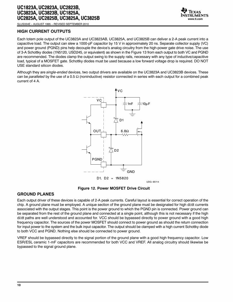
HIGH CURRENT OUTPUTS
Each totem pole output of the UC3823A and UC3823AB, UC3825A, and UC3825B can deliver a 2-A peak current into acapacitive load. The output can slew a 1000-pF capacitor by 15 V in approximately 20 ns. Separate collector supply (VC)and power ground (PGND) pins help decouple the device’s analog circuitry from the high-power gate drive noise. The useof 3-A Schottky diodes (1N5120, USD245, or equivalent) as shown in the Figure 13 from each output to both VC and PGNDare recommended. The diodes clamp the output swing to the supply rails, necessary with any type of inductive/capacitiveload, typical of a MOSFET gate. Schottky diodes must be used because a low forward voltage drop is required. DO NOTUSE standard silicon diodes.
Although they are single-ended devices, two output drivers are available on the UC3823A and UC3823B devices. Thesecan be paralleled by the use of a 0.5 Ω (noninductive) resistor connected in series with each output for a combined peakcurrent of 4 A.
UDG−95114
Figure 12. Power MOSFET Drive Circuit
GROUND PLANESEach output driver of these devices is capable of 2-A peak currents. Careful layout is essential for correct operation of thechip. A ground plane must be employed. A unique section of the ground plane must be designated for high di/dt currentsassociated with the output stages. This point is the power ground to which the PGND pin is connected. Power ground canbe separated from the rest of the ground plane and connected at a single point, although this is not necessary if the highdi/dt paths are well understood and accounted for. VCC should be bypassed directly to power ground with a good highfrequency capacitor. The sources of the power MOSFET should connect to power ground as should the return connectionfor input power to the system and the bulk input capacitor. The output should be clamped with a high current Schottky diodeto both VCC and PGND. Nothing else should be connected to power ground.
VREF should be bypassed directly to the signal portion of the ground plane with a good high frequency capacitor. LowESR/ESL ceramic 1-mF capacitors are recommended for both VCC and VREF. All analog circuitry should likewise bebypassed to the signal ground plane.
UC1823A, UC2823A, UC2823B,UC3823A, UC3823B, UC1825A,
UC2825A, UC2825B, UC3825A, UC3825BSLUS334E − AUGUST 1995 − REVISED SEPTEMBER 2010
www.ti.com
11
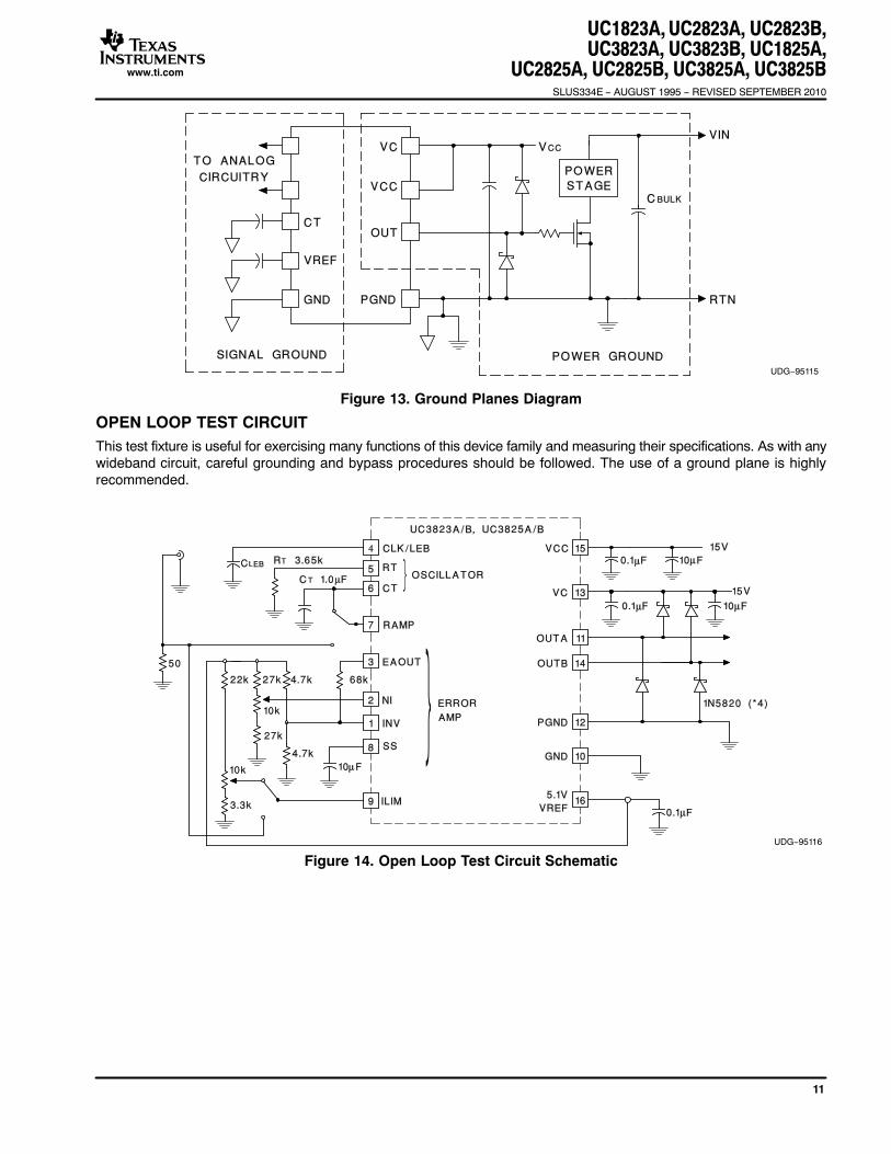
UDG−95115
Figure 13. Ground Planes Diagram
OPEN LOOP TEST CIRCUITThis test fixture is useful for exercising many functions of this device family and measuring their specifications. As with anywideband circuit, careful grounding and bypass procedures should be followed. The use of a ground plane is highlyrecommended.
UDG−95116
Figure 14. Open Loop Test Circuit Schematic
PACKAGE OPTION ADDENDUM
www.ti.com 12-Oct-2021
Addendum-Page 1
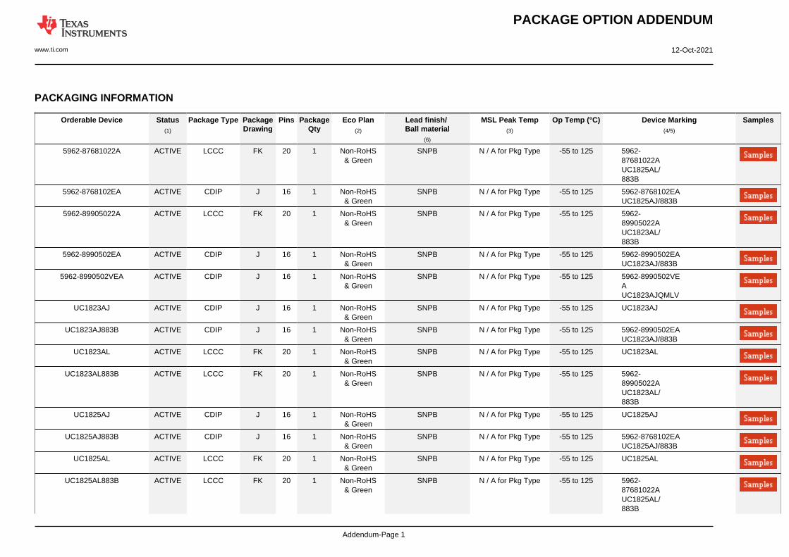
PACKAGING INFORMATION
Orderable Device Status(1)
Package Type PackageDrawing
Pins PackageQty
Eco Plan(2)
Lead finish/Ball material
(6)
MSL Peak Temp(3)
Op Temp (°C) Device Marking(4/5)
Samples
5962-87681022A ACTIVE LCCC FK 20 1 Non-RoHS& Green
SNPB N / A for Pkg Type -55 to 125 5962-87681022AUC1825AL/883B
5962-8768102EA ACTIVE CDIP J 16 1 Non-RoHS& Green
SNPB N / A for Pkg Type -55 to 125 5962-8768102EAUC1825AJ/883B
5962-89905022A ACTIVE LCCC FK 20 1 Non-RoHS& Green
SNPB N / A for Pkg Type -55 to 125 5962-89905022AUC1823AL/883B
5962-8990502EA ACTIVE CDIP J 16 1 Non-RoHS& Green
SNPB N / A for Pkg Type -55 to 125 5962-8990502EAUC1823AJ/883B
5962-8990502VEA ACTIVE CDIP J 16 1 Non-RoHS& Green
SNPB N / A for Pkg Type -55 to 125 5962-8990502VEAUC1823AJQMLV
UC1823AJ ACTIVE CDIP J 16 1 Non-RoHS& Green
SNPB N / A for Pkg Type -55 to 125 UC1823AJ
UC1823AJ883B ACTIVE CDIP J 16 1 Non-RoHS& Green
SNPB N / A for Pkg Type -55 to 125 5962-8990502EAUC1823AJ/883B
UC1823AL ACTIVE LCCC FK 20 1 Non-RoHS& Green
SNPB N / A for Pkg Type -55 to 125 UC1823AL
UC1823AL883B ACTIVE LCCC FK 20 1 Non-RoHS& Green
SNPB N / A for Pkg Type -55 to 125 5962-89905022AUC1823AL/883B
UC1825AJ ACTIVE CDIP J 16 1 Non-RoHS& Green
SNPB N / A for Pkg Type -55 to 125 UC1825AJ
UC1825AJ883B ACTIVE CDIP J 16 1 Non-RoHS& Green
SNPB N / A for Pkg Type -55 to 125 5962-8768102EAUC1825AJ/883B
UC1825AL ACTIVE LCCC FK 20 1 Non-RoHS& Green
SNPB N / A for Pkg Type -55 to 125 UC1825AL
UC1825AL883B ACTIVE LCCC FK 20 1 Non-RoHS& Green
SNPB N / A for Pkg Type -55 to 125 5962-87681022AUC1825AL/883B
PACKAGE OPTION ADDENDUM
www.ti.com 12-Oct-2021
Addendum-Page 2
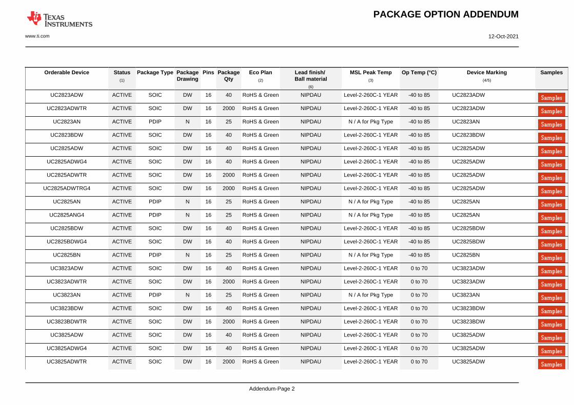
Orderable Device Status(1)
Package Type PackageDrawing
Pins PackageQty
Eco Plan(2)
Lead finish/Ball material
(6)
MSL Peak Temp(3)
Op Temp (°C) Device Marking(4/5)
Samples
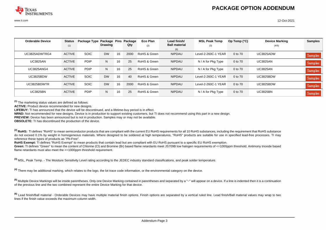
UC2823ADW ACTIVE SOIC DW 16 40 RoHS & Green NIPDAU Level-2-260C-1 YEAR -40 to 85 UC2823ADW
UC2823ADWTR ACTIVE SOIC DW 16 2000 RoHS & Green NIPDAU Level-2-260C-1 YEAR -40 to 85 UC2823ADW
UC2823AN ACTIVE PDIP N 16 25 RoHS & Green NIPDAU N / A for Pkg Type -40 to 85 UC2823AN
UC2823BDW ACTIVE SOIC DW 16 40 RoHS & Green NIPDAU Level-2-260C-1 YEAR -40 to 85 UC2823BDW
UC2825ADW ACTIVE SOIC DW 16 40 RoHS & Green NIPDAU Level-2-260C-1 YEAR -40 to 85 UC2825ADW
UC2825ADWG4 ACTIVE SOIC DW 16 40 RoHS & Green NIPDAU Level-2-260C-1 YEAR -40 to 85 UC2825ADW
UC2825ADWTR ACTIVE SOIC DW 16 2000 RoHS & Green NIPDAU Level-2-260C-1 YEAR -40 to 85 UC2825ADW
UC2825ADWTRG4 ACTIVE SOIC DW 16 2000 RoHS & Green NIPDAU Level-2-260C-1 YEAR -40 to 85 UC2825ADW
UC2825AN ACTIVE PDIP N 16 25 RoHS & Green NIPDAU N / A for Pkg Type -40 to 85 UC2825AN
UC2825ANG4 ACTIVE PDIP N 16 25 RoHS & Green NIPDAU N / A for Pkg Type -40 to 85 UC2825AN
UC2825BDW ACTIVE SOIC DW 16 40 RoHS & Green NIPDAU Level-2-260C-1 YEAR -40 to 85 UC2825BDW
UC2825BDWG4 ACTIVE SOIC DW 16 40 RoHS & Green NIPDAU Level-2-260C-1 YEAR -40 to 85 UC2825BDW
UC2825BN ACTIVE PDIP N 16 25 RoHS & Green NIPDAU N / A for Pkg Type -40 to 85 UC2825BN
UC3823ADW ACTIVE SOIC DW 16 40 RoHS & Green NIPDAU Level-2-260C-1 YEAR 0 to 70 UC3823ADW
UC3823ADWTR ACTIVE SOIC DW 16 2000 RoHS & Green NIPDAU Level-2-260C-1 YEAR 0 to 70 UC3823ADW
UC3823AN ACTIVE PDIP N 16 25 RoHS & Green NIPDAU N / A for Pkg Type 0 to 70 UC3823AN
UC3823BDW ACTIVE SOIC DW 16 40 RoHS & Green NIPDAU Level-2-260C-1 YEAR 0 to 70 UC3823BDW
UC3823BDWTR ACTIVE SOIC DW 16 2000 RoHS & Green NIPDAU Level-2-260C-1 YEAR 0 to 70 UC3823BDW
UC3825ADW ACTIVE SOIC DW 16 40 RoHS & Green NIPDAU Level-2-260C-1 YEAR 0 to 70 UC3825ADW
UC3825ADWG4 ACTIVE SOIC DW 16 40 RoHS & Green NIPDAU Level-2-260C-1 YEAR 0 to 70 UC3825ADW
UC3825ADWTR ACTIVE SOIC DW 16 2000 RoHS & Green NIPDAU Level-2-260C-1 YEAR 0 to 70 UC3825ADW
PACKAGE OPTION ADDENDUM
www.ti.com 12-Oct-2021
Addendum-Page 3
Orderable Device Status(1)
Package Type PackageDrawing
Pins PackageQty
Eco Plan(2)
Lead finish/Ball material
(6)
MSL Peak Temp(3)
Op Temp (°C) Device Marking(4/5)
Samples
UC3825ADWTRG4 ACTIVE SOIC DW 16 2000 RoHS & Green NIPDAU Level-2-260C-1 YEAR 0 to 70 UC3825ADW
UC3825AN ACTIVE PDIP N 16 25 RoHS & Green NIPDAU N / A for Pkg Type 0 to 70 UC3825AN
UC3825ANG4 ACTIVE PDIP N 16 25 RoHS & Green NIPDAU N / A for Pkg Type 0 to 70 UC3825AN
UC3825BDW ACTIVE SOIC DW 16 40 RoHS & Green NIPDAU Level-2-260C-1 YEAR 0 to 70 UC3825BDW
UC3825BDWTR ACTIVE SOIC DW 16 2000 RoHS & Green NIPDAU Level-2-260C-1 YEAR 0 to 70 UC3825BDW
UC3825BN ACTIVE PDIP N 16 25 RoHS & Green NIPDAU N / A for Pkg Type 0 to 70 UC3825BN
(1) The marketing status values are defined as follows:ACTIVE: Product device recommended for new designs.LIFEBUY: TI has announced that the device will be discontinued, and a lifetime-buy period is in effect.NRND: Not recommended for new designs. Device is in production to support existing customers, but TI does not recommend using this part in a new design.PREVIEW: Device has been announced but is not in production. Samples may or may not be available.OBSOLETE: TI has discontinued the production of the device.
(2) RoHS: TI defines "RoHS" to mean semiconductor products that are compliant with the current EU RoHS requirements for all 10 RoHS substances, including the requirement that RoHS substancedo not exceed 0.1% by weight in homogeneous materials. Where designed to be soldered at high temperatures, "RoHS" products are suitable for use in specified lead-free processes. TI mayreference these types of products as "Pb-Free".RoHS Exempt: TI defines "RoHS Exempt" to mean products that contain lead but are compliant with EU RoHS pursuant to a specific EU RoHS exemption.Green: TI defines "Green" to mean the content of Chlorine (Cl) and Bromine (Br) based flame retardants meet JS709B low halogen requirements of <=1000ppm threshold. Antimony trioxide basedflame retardants must also meet the <=1000ppm threshold requirement.
(3) MSL, Peak Temp. - The Moisture Sensitivity Level rating according to the JEDEC industry standard classifications, and peak solder temperature.
(4) There may be additional marking, which relates to the logo, the lot trace code information, or the environmental category on the device.
(5) Multiple Device Markings will be inside parentheses. Only one Device Marking contained in parentheses and separated by a "~" will appear on a device. If a line is indented then it is a continuationof the previous line and the two combined represent the entire Device Marking for that device.
(6) Lead finish/Ball material - Orderable Devices may have multiple material finish options. Finish options are separated by a vertical ruled line. Lead finish/Ball material values may wrap to twolines if the finish value exceeds the maximum column width.
PACKAGE OPTION ADDENDUM
www.ti.com 12-Oct-2021
Addendum-Page 4
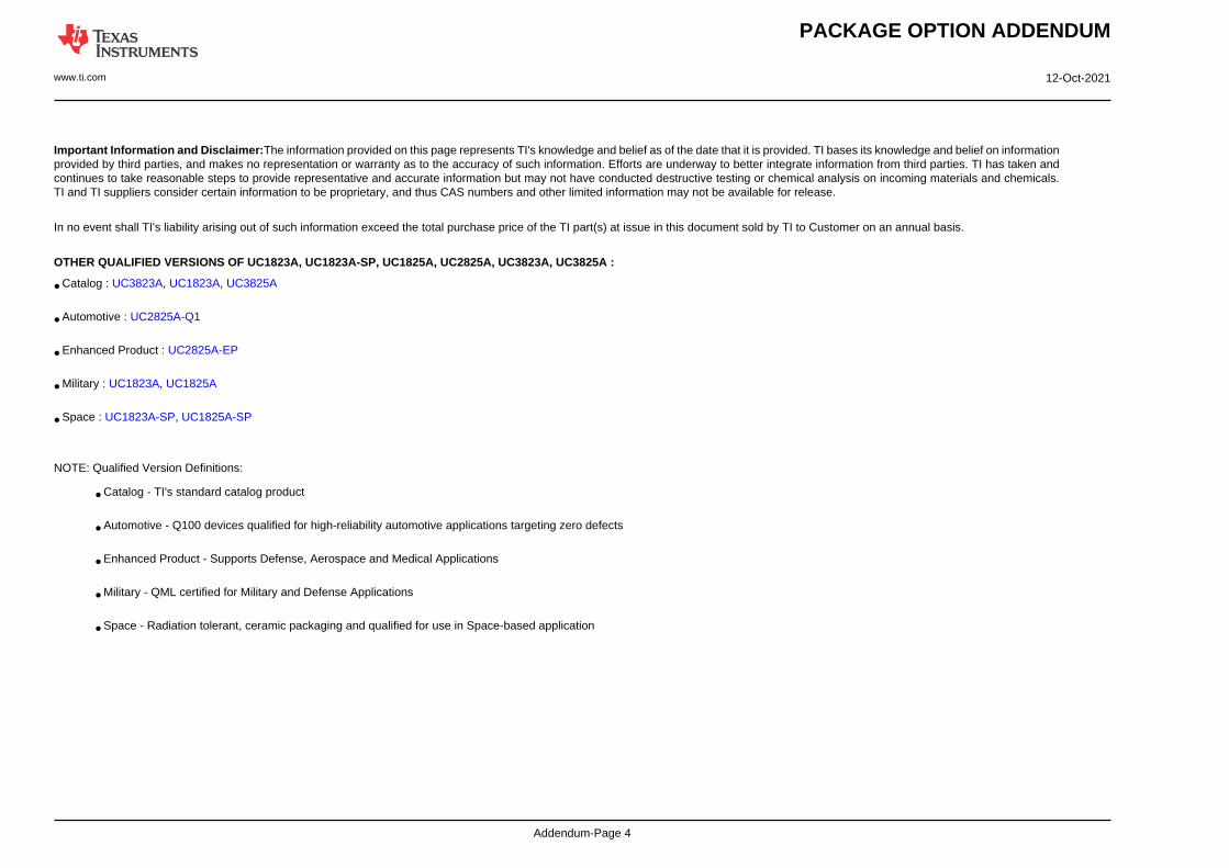
Important Information and Disclaimer:The information provided on this page represents TI's knowledge and belief as of the date that it is provided. TI bases its knowledge and belief on informationprovided by third parties, and makes no representation or warranty as to the accuracy of such information. Efforts are underway to better integrate information from third parties. TI has taken andcontinues to take reasonable steps to provide representative and accurate information but may not have conducted destructive testing or chemical analysis on incoming materials and chemicals.TI and TI suppliers consider certain information to be proprietary, and thus CAS numbers and other limited information may not be available for release.
In no event shall TI's liability arising out of such information exceed the total purchase price of the TI part(s) at issue in this document sold by TI to Customer on an annual basis.
OTHER QUALIFIED VERSIONS OF UC1823A, UC1823A-SP, UC1825A, UC2825A, UC3823A, UC3825A :
• Catalog : UC3823A, UC1823A, UC3825A
• Automotive : UC2825A-Q1
• Enhanced Product : UC2825A-EP
• Military : UC1823A, UC1825A
• Space : UC1823A-SP, UC1825A-SP
NOTE: Qualified Version Definitions:
• Catalog - TI's standard catalog product
• Automotive - Q100 devices qualified for high-reliability automotive applications targeting zero defects
• Enhanced Product - Supports Defense, Aerospace and Medical Applications
• Military - QML certified for Military and Defense Applications
• Space - Radiation tolerant, ceramic packaging and qualified for use in Space-based application
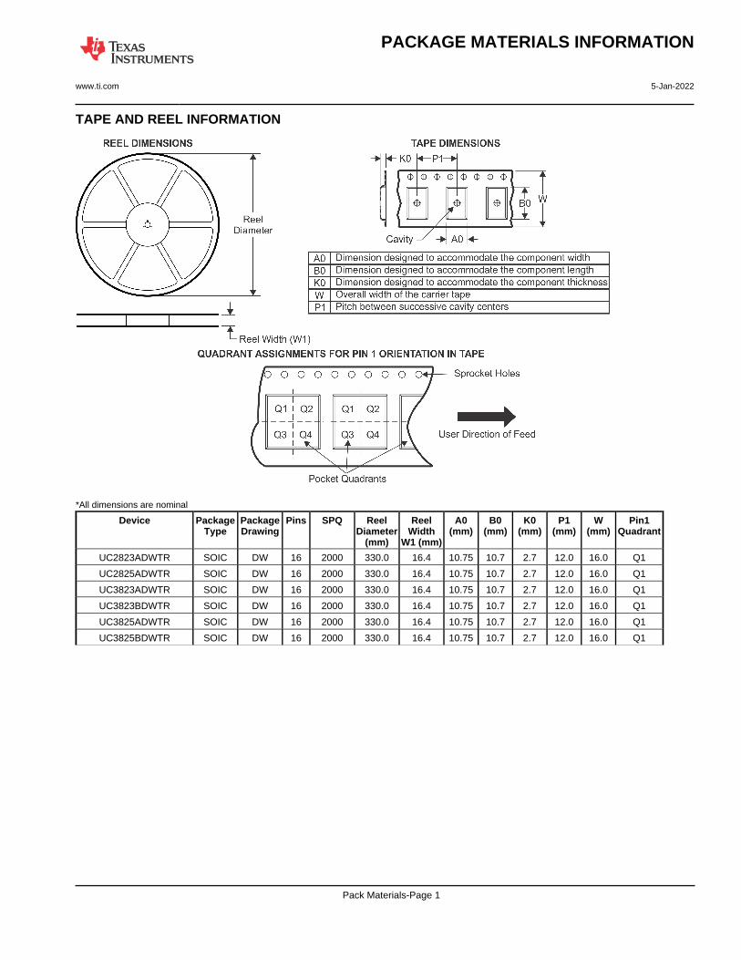
TAPE AND REEL INFORMATION
*All dimensions are nominal
Device PackageType
PackageDrawing
Pins SPQ ReelDiameter
(mm)
ReelWidth
W1 (mm)
A0(mm)
B0(mm)
K0(mm)
P1(mm)
W(mm)
Pin1Quadrant
UC2823ADWTR SOIC DW 16 2000 330.0 16.4 10.75 10.7 2.7 12.0 16.0 Q1
UC2825ADWTR SOIC DW 16 2000 330.0 16.4 10.75 10.7 2.7 12.0 16.0 Q1
UC3823ADWTR SOIC DW 16 2000 330.0 16.4 10.75 10.7 2.7 12.0 16.0 Q1
UC3823BDWTR SOIC DW 16 2000 330.0 16.4 10.75 10.7 2.7 12.0 16.0 Q1
UC3825ADWTR SOIC DW 16 2000 330.0 16.4 10.75 10.7 2.7 12.0 16.0 Q1
UC3825BDWTR SOIC DW 16 2000 330.0 16.4 10.75 10.7 2.7 12.0 16.0 Q1
PACKAGE MATERIALS INFORMATION
www.ti.com 5-Jan-2022
Pack Materials-Page 1
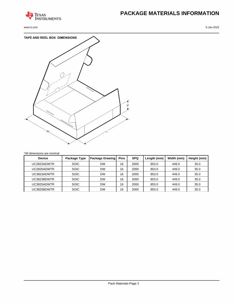
*All dimensions are nominal
Device Package Type Package Drawing Pins SPQ Length (mm) Width (mm) Height (mm)
UC2823ADWTR SOIC DW 16 2000 853.0 449.0 35.0
UC2825ADWTR SOIC DW 16 2000 853.0 449.0 35.0
UC3823ADWTR SOIC DW 16 2000 853.0 449.0 35.0
UC3823BDWTR SOIC DW 16 2000 853.0 449.0 35.0
UC3825ADWTR SOIC DW 16 2000 853.0 449.0 35.0
UC3825BDWTR SOIC DW 16 2000 853.0 449.0 35.0
PACKAGE MATERIALS INFORMATION
www.ti.com 5-Jan-2022
Pack Materials-Page 2
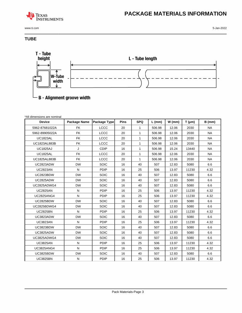
TUBE
*All dimensions are nominal
Device Package Name Package Type Pins SPQ L (mm) W (mm) T (µm) B (mm)
5962-87681022A FK LCCC 20 1 506.98 12.06 2030 NA
5962-89905022A FK LCCC 20 1 506.98 12.06 2030 NA
UC1823AL FK LCCC 20 1 506.98 12.06 2030 NA
UC1823AL883B FK LCCC 20 1 506.98 12.06 2030 NA
UC1825AJ J CDIP 16 1 506.98 15.24 13440 NA
UC1825AL FK LCCC 20 1 506.98 12.06 2030 NA
UC1825AL883B FK LCCC 20 1 506.98 12.06 2030 NA
UC2823ADW DW SOIC 16 40 507 12.83 5080 6.6
UC2823AN N PDIP 16 25 506 13.97 11230 4.32
UC2823BDW DW SOIC 16 40 507 12.83 5080 6.6
UC2825ADW DW SOIC 16 40 507 12.83 5080 6.6
UC2825ADWG4 DW SOIC 16 40 507 12.83 5080 6.6
UC2825AN N PDIP 16 25 506 13.97 11230 4.32
UC2825ANG4 N PDIP 16 25 506 13.97 11230 4.32
UC2825BDW DW SOIC 16 40 507 12.83 5080 6.6
UC2825BDWG4 DW SOIC 16 40 507 12.83 5080 6.6
UC2825BN N PDIP 16 25 506 13.97 11230 4.32
UC3823ADW DW SOIC 16 40 507 12.83 5080 6.6
UC3823AN N PDIP 16 25 506 13.97 11230 4.32
UC3823BDW DW SOIC 16 40 507 12.83 5080 6.6
UC3825ADW DW SOIC 16 40 507 12.83 5080 6.6
UC3825ADWG4 DW SOIC 16 40 507 12.83 5080 6.6
UC3825AN N PDIP 16 25 506 13.97 11230 4.32
UC3825ANG4 N PDIP 16 25 506 13.97 11230 4.32
UC3825BDW DW SOIC 16 40 507 12.83 5080 6.6
UC3825BN N PDIP 16 25 506 13.97 11230 4.32
PACKAGE MATERIALS INFORMATION
www.ti.com 5-Jan-2022
Pack Materials-Page 3
IMPORTANT NOTICE AND DISCLAIMERTI PROVIDES TECHNICAL AND RELIABILITY DATA (INCLUDING DATA SHEETS), DESIGN RESOURCES (INCLUDING REFERENCE DESIGNS), APPLICATION OR OTHER DESIGN ADVICE, WEB TOOLS, SAFETY INFORMATION, AND OTHER RESOURCES “AS IS” AND WITH ALL FAULTS, AND DISCLAIMS ALL WARRANTIES, EXPRESS AND IMPLIED, INCLUDING WITHOUT LIMITATION ANY IMPLIED WARRANTIES OF MERCHANTABILITY, FITNESS FOR A PARTICULAR PURPOSE OR NON-INFRINGEMENT OF THIRD PARTY INTELLECTUAL PROPERTY RIGHTS.These resources are intended for skilled developers designing with TI products. You are solely responsible for (1) selecting the appropriate TI products for your application, (2) designing, validating and testing your application, and (3) ensuring your application meets applicable standards, and any other safety, security, regulatory or other requirements.These resources are subject to change without notice. TI grants you permission to use these resources only for development of an application that uses the TI products described in the resource. Other reproduction and display of these resources is prohibited. No license is granted to any other TI intellectual property right or to any third party intellectual property right. TI disclaims responsibility for, and you will fully indemnify TI and its representatives against, any claims, damages, costs, losses, and liabilities arising out of your use of these resources.TI’s products are provided subject to TI’s Terms of Sale or other applicable terms available either on ti.com or provided in conjunction with such TI products. TI’s provision of these resources does not expand or otherwise alter TI’s applicable warranties or warranty disclaimers for TI products.TI objects to and rejects any additional or different terms you may have proposed. IMPORTANT NOTICE
Mailing Address: Texas Instruments, Post Office Box 655303, Dallas, Texas 75265Copyright © 2022, Texas Instruments Incorporated