Design of Buck Converter
12
Design of Buck Converter Presented by, B. Naveen 207215001 Akhil S. 207215002 1
-
Upload
akhil-syamalan -
Category
Engineering
-
view
1.362 -
download
7
Transcript of Design of Buck Converter
1
Design of Buck Converter
Presented by,
B. Naveen 207215001
Akhil S. 207215002
Design of Buck converter 2
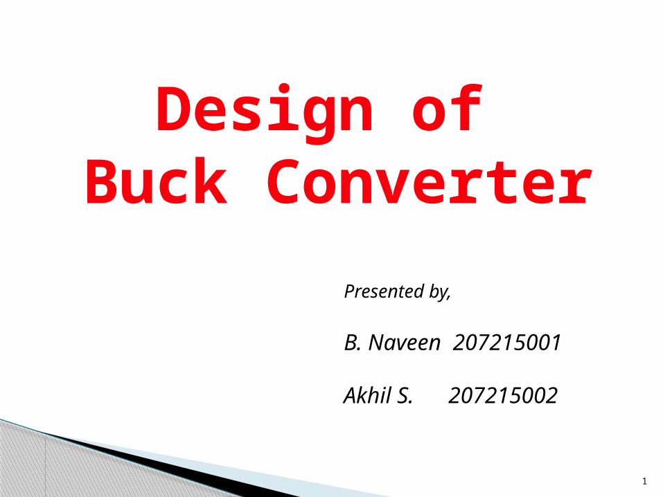
Design ProblemDesign a buck converter satisfying the following requirements: Input Voltage, Vin=12V Output Voltage, Vout=5V Output Current, Io=2A Switching frequency, fsw=400kHz Ripple current, ΔIL=30% of IL (max.) Ripple voltage, ΔVo=50mV (max.)
Fig.1: Buck converter circuit arrangement
Design of Buck converter 3
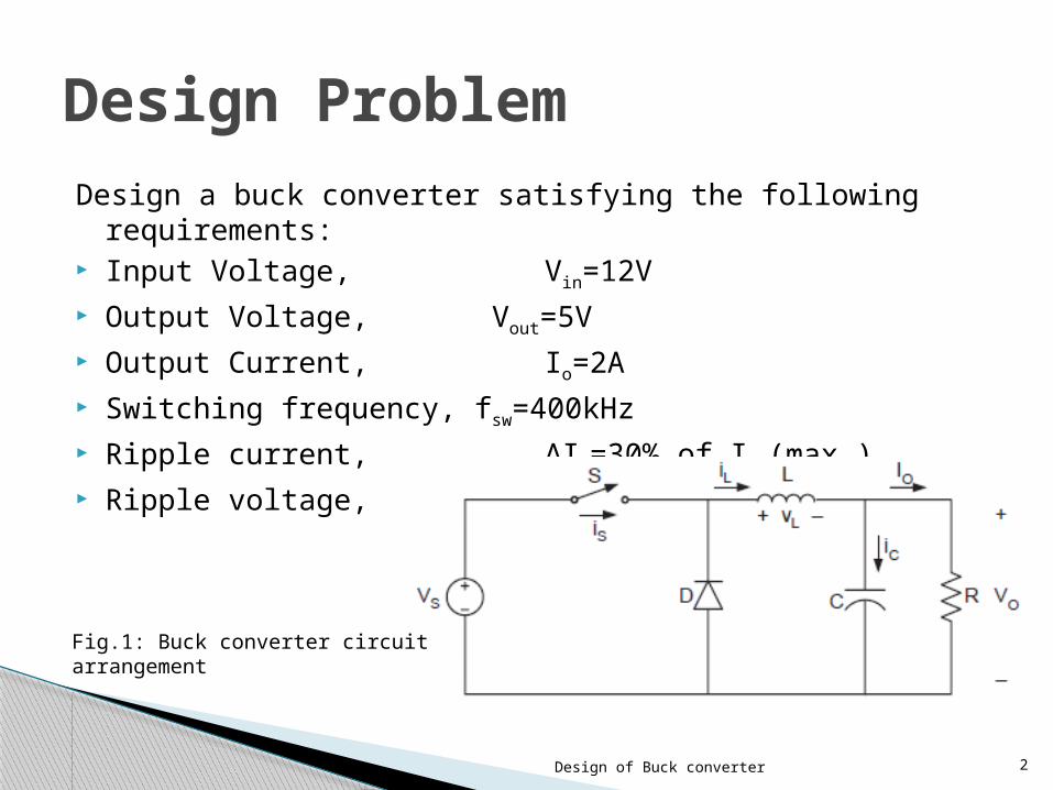
Loadresistance,RL =VO/ ILOAD=5/ 2=2.5X
Ripplecurrent,IRIPPLE =3 IL =0.3#ILOAD =0.3#2=0.6A
Outputvoltage,VO =DVIN
` Duty ratio, D =VINVO
=125
=0.4166
T =1/ fsw =400* 1031 =2.5n sec
TON =DT =0.4166* 2.5n =1.04n sec
TOFF =(1- D)T =(1- 0.4166)2.5n=1.45n sec
Initial Calculations
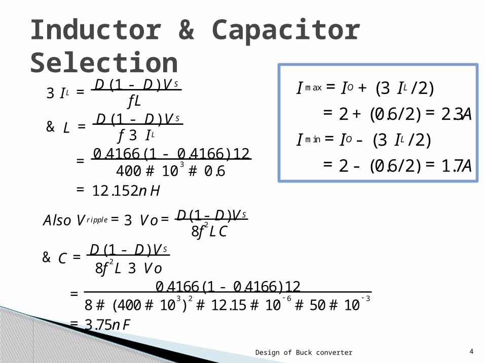
Design of Buck converter 4
3 IL = fLD(1- D)VS
& L = f 3 ILD(1- D)VS
= 400#103 #0.60.4166(1- 0.4166)12
=12.152nHAlso Vripple=3 Vo= 8f2LC
D(1- D)VS
& C= 8f2L 3 VoD(1- D)VS
=8#(400#103) 2 #12.15#10- 6 #50#10- 30.4166(1- 0.4166)12
=3.75nF
Inductor & Capacitor Selection
I max =IO +(3 IL/ 2)=2+(0.6/ 2) =2.3A
I min =IO - (3 IL/ 2)=2- (0.6/ 2) =1.7A
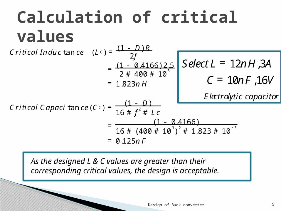
Design of Buck converter 5
Critical Inductance (LC) = 2f(1- D)R
= 2#400#103(1- 0.4166)2.5
=1.823nH
Critical Capaci tance(CC) =16#f2 #Lc(1- D)
=16#(400#103) 2 #1.823#10- 3(1- 0.4166)
=0.125nF
As the designed L & C values are greater than their corresponding critical values, the design is acceptable.
Calculation of critical values
SelectL =12nH,3AC=10nF,16VElectrolytic capacitor
Design of Buck converter 6
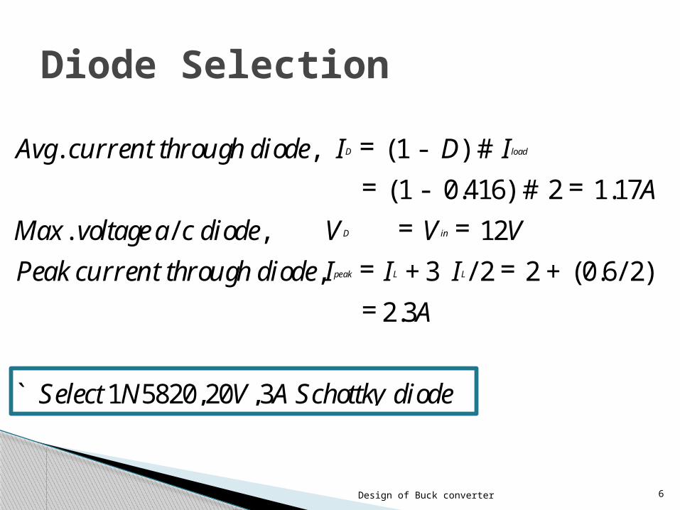
Diode SelectionAvg. currentthroughdiode, ID =(1- D) #I load
=(1- 0.416) #2=1.17AMax. voltagea/cdiode, VD =Vin =12VPeakcurrentthroughdiode,Ipeak =IL +3 IL/ 2=2+(0.6/ 2)
=2.3A
` Select1N5820,20V,3ASchottkydiode
Design of Buck converter 7
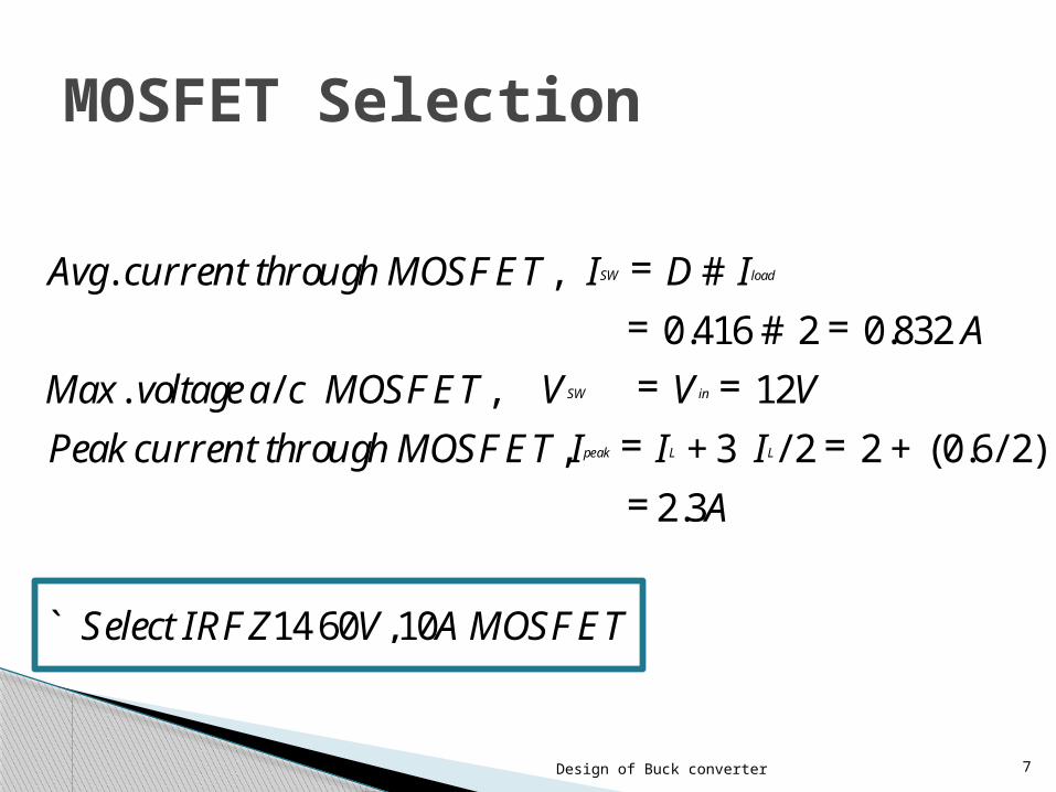
MOSFET Selection
Avg. currentthroughMOSFET, ISW =D#I load=0.416#2=0.832A
Max.voltagea/c MOSFET, VSW =Vin =12VPeakcurrentthroughMOSFET,Ipeak =IL +3 IL/ 2=2+(0.6/2)
=2.3A
` SelectIRFZ1460V,10AMOSFET
Design of Buck converter 8
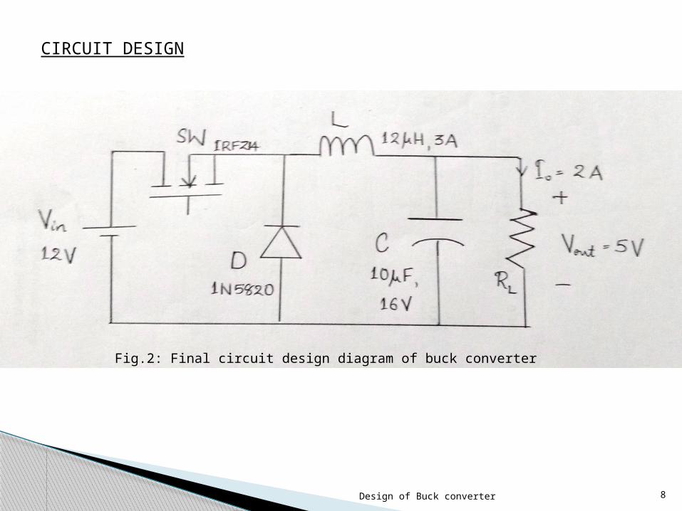
CIRCUIT DESIGN
Fig.2: Final circuit design diagram of buck converter
Design of Buck converter 9
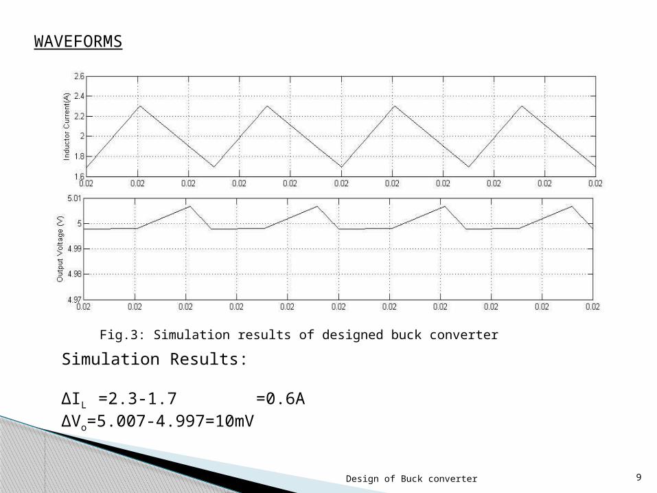
WAVEFORMS
Fig.3: Simulation results of designed buck converter
Simulation Results:
ΔIL =2.3-1.7 =0.6AΔVo=5.007-4.997=10mV
Design of Buck converter 10
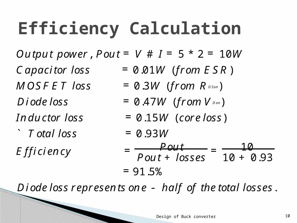
Efficiency CalculationOutput power, Pout=V#I =5* 2=10WCapacitor loss =0.01W (fromESR)MOSFET loss =0.3W (fromRDSon)Diodeloss =0.47W (fromVDon)Inductor loss =0.15W (coreloss)` Total loss =0.93WEfficiency =Pout+losses
Pout =10+0.9310
=91.5%Diodelossrepresentsone- half of thetotal losses.
Design of Buck converter 11
[1] Ned Mohan, Undeland and Robbin, ‘Power Electronics: Converters, Application and Design’, John Wiley and sons Inc., Newyork,2006.
[2] Rashid M.H., ‘Power Electronics- Circuits, Device and Applications’, Prentice Hall India, New Delhi, 2009.
[3] Datasheets 1N5820 http://www.farnell.com/datasheets/107972.pdf IRFZ14 http://www.irf.com/product-info/datasheets/data/irfz14.pdf Capacitor http://www.farnell.com/datasheets/1558295.pdf
References

Design of Buck converter 12
THANK YOU