


γλώσσες
Σελίδες
Νομικός


Status of BELLE upgradeYoshikazu YAMADA (KEK-IPNS)at 44th KEKB Suishin Iinkai on June 11, 2001
• Upgrade Points of Inner Tracker• New Beam Pipe for IP• SVD2• Small Cell Chamber
1. Upgrade Points of Inner Tracker•Better impact parameter resolution
Rbp : 2.0 cm→→→→ 1.5 cm ���� σσσσ∆∆∆∆z : 100 µµµµm →→→→ 75 µµµµm•Larger acceptance for SVD
Ladder length : 22 cm →→→→ 46 cm ���� 23º < θθθθ < 139º →→→→ 17º < θθθθ < 150º•Better tracking efficiency
RSVD-outermost : 6.0 cm→→→→ 8.8 cm ���� eff. of slow π :π :π :π :54 % →→→→ 77 %•More radiation hardness for SVD
VA1−−−−0.8 µµµµm →→→→ VA1−−−−0.35 µµµµm ���� 1 MRad →→→→ >5 MRad•Better trigger capability
•VA1 →→→→ VA1TA (VA1 with trigger)•Introduction of Level−−−−1.5 trigger in SVD FADC system•Introduction of Small cell chamber•Faster SVD / CDCsmallcell electronics���� trigger rate @ design current : 1400 Hz →→→→ 500? Hz
•Installation in Summer 2002
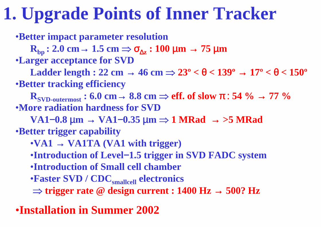
Design modificationBeam pipe : Rin = 2.0 cmSVD1 : R = 3.0, 4.5, 6.0 cmCDC : 3 layers of Cathode part
Beam pipe : Rin = 1.5 cmSVD2 : R = 2.0, 4.35, 7.0, 8.8 cmCDC : 2 layers of small cell chamber
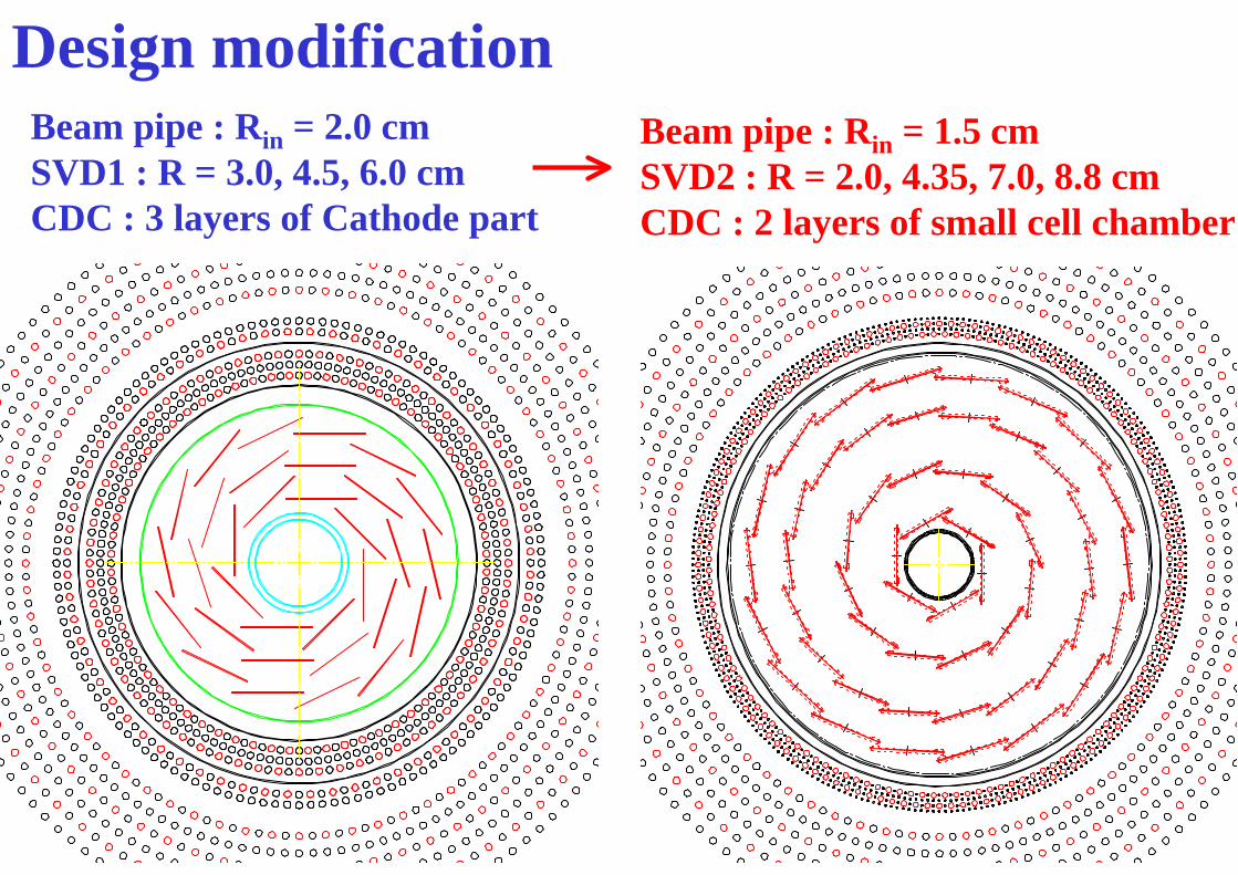
Acceptance
17 º < θθθθ < 150 º
23 º < θθθθ < 139 º
2. New beam pipe for IP
~3.6~1.5~3≡≡≡≡1CDC 1st layer Occup.~660~80~130~40SVD 1st layer dose(krad/yr=107s)
~ 8~ 0.9~3≡≡≡≡1SVD 1st layer Occup.~75
4/2.0cm
SVD2Rbp=1.5cm
@design current
SVD2Rbp=1.0cm
@design current
SVD1.4Rbp=2.0cm
@design current
SVD1.4Rbp=2.0cm@ 0.6/0.8A
~50××××1.3?~100××××1.2?~100σσσσ∆∆∆∆Z (µµµµm)
5/1.5cm3/3.0cm3/3.0cm# of layers/R1st
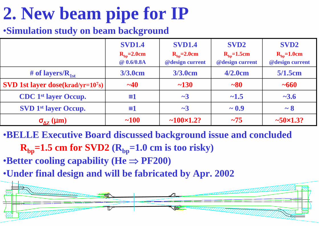
•BELLE Executive Board discussed background issue and concluded Rbp=1.5 cm for SVD2 (Rbp=1.0 cm is too risky)
•Better cooling capability (He ���� PF200)•Under final design and will be fabricated by Apr. 2002
•Simulation study on beam background
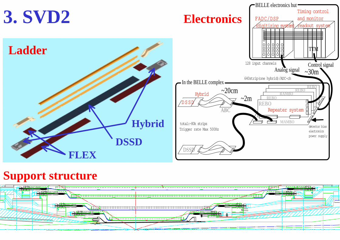
~20cmHybrid
DSSD
ABC
DSSD
~2mREBO
MAMBO
REBO
REBOREBO
RAMBO
TTM
FADC/DSP(digitizing system)
Timing controland monitorreadout system
~30m
detector biaselectronicspower supply
total:~80k stripsTrigger rate Max 500Hz
128 input channels Control signalAnalog signal
640strip(one hybrid)/ADC-ch
Repeater system
BELLE electronics hut
In the BELLE complex
3. SVD2
DSSDFLEX
Hybrid
Ladder
Support structure
Electronics
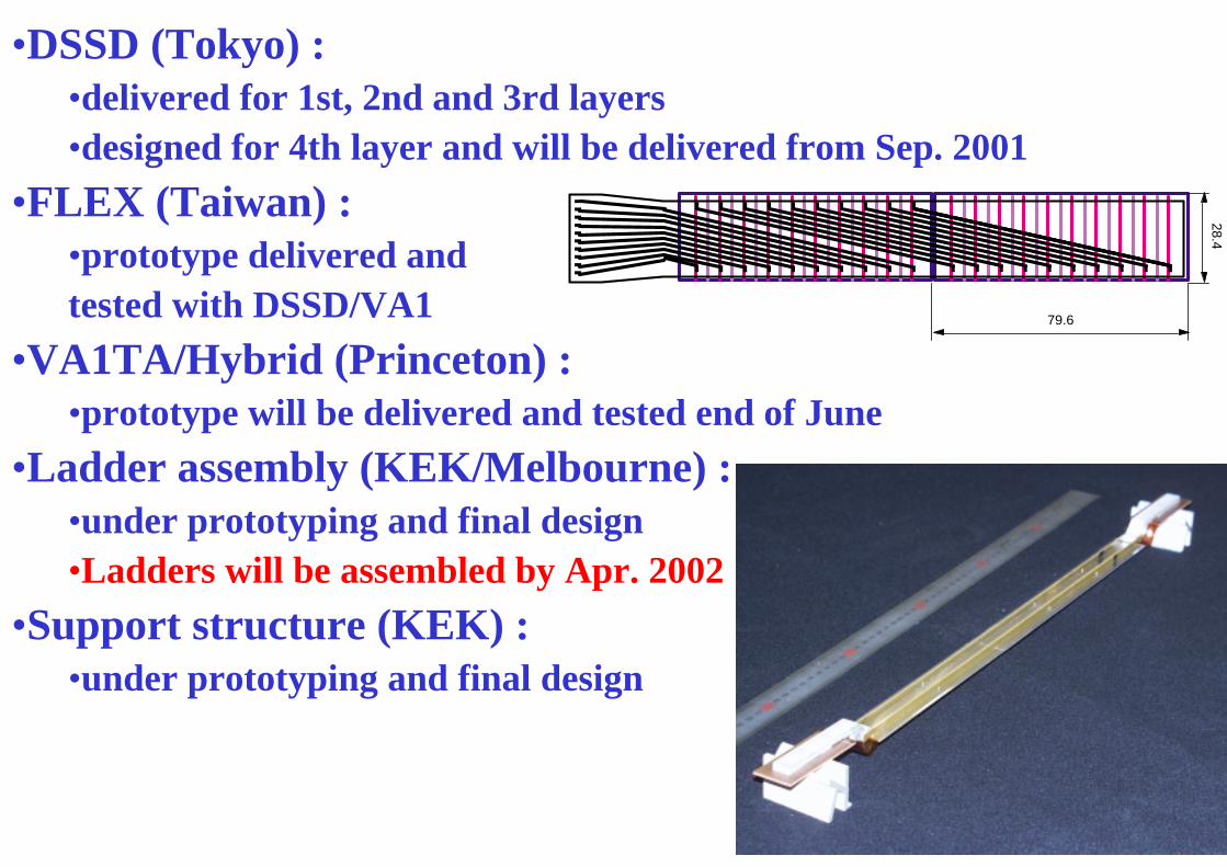
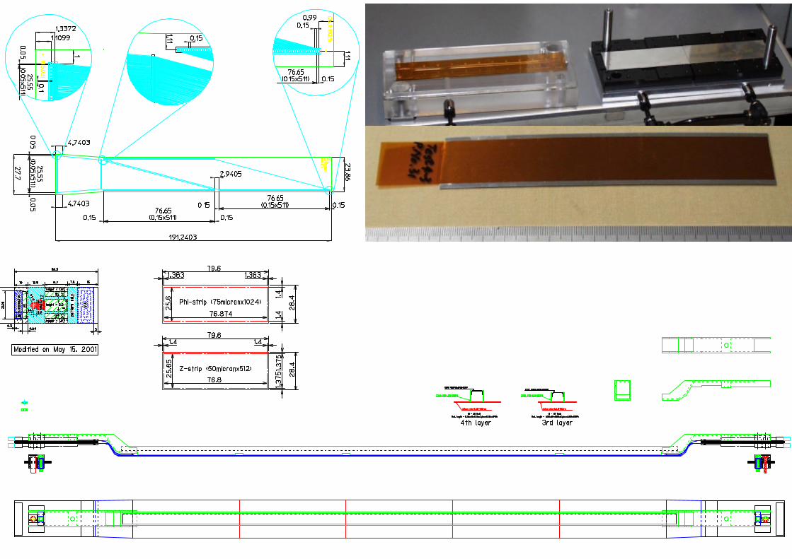
•DSSD (Tokyo) : •delivered for 1st, 2nd and 3rd layers•designed for 4th layer and will be delivered from Sep. 2001
•FLEX (Taiwan) : •prototype delivered andtested with DSSD/VA1
•VA1TA/Hybrid (Princeton) :•prototype will be delivered and tested end of June
•Ladder assembly (KEK/Melbourne) :•under prototyping and final design•Ladders will be assembled by Apr. 2002
•Support structure (KEK) :•under prototyping and final design
79.6
28.4
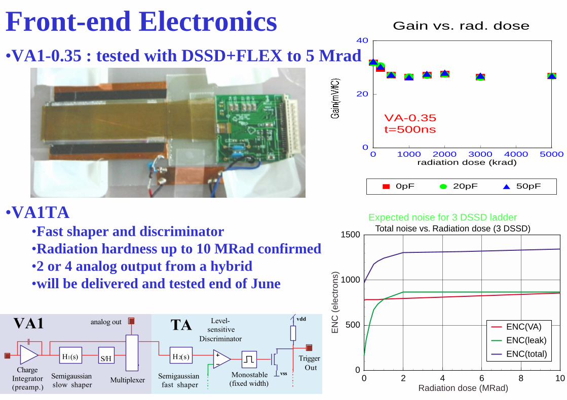
Front-end Electronics
Level- sensitive
Discriminator
Semigaussian fast shaper
Monostable (fixed width)
Semigaussian slow shaper
Charge Integrator (preamp.)
S/H H 1 (s) H 2 (s)
vss
vdd
TriggerOut
TAVA1
Multiplexer
analog out
0
20
40
0 1000 2000 3000 4000 5000radiation dose (krad)
0pF 20pF 50pF
VA-0.35t=500ns
Gain vs. rad. dose
•VA1TA•Fast shaper and discriminator•Radiation hardness up to 10 MRad confirmed•2 or 4 analog output from a hybrid•will be delivered and tested end of June
0
500
1000
1500
0 2 4 6 8 10
EN
C (
elec
tron
s)
Radiation dose (MRad)
ENC(VA)
ENC(leak)
ENC(total)
Total noise vs. Radiation dose (3 DSSD)Expected noise for 3 DSSD ladder
•VA1-0.35 : tested with DSSD+FLEX to 5 Mrad
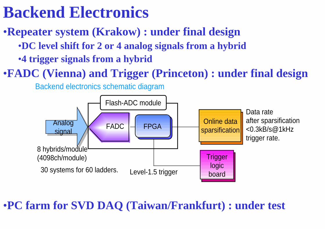
Backend Electronics
FADCOnline data
sparsification
Triggerlogicboard
Analogsignal
FPGA
Level-1.5 trigger
Flash-ADC module
8 hybrids/module(4098ch/module)
30 systems for 60 ladders.
Data rate after sparsification<0.3kB/s@1kHz trigger rate.
Backend electronics schematic diagram
•Repeater system (Krakow) : under final design•DC level shift for 2 or 4 analog signals from a hybrid •4 trigger signals from a hybrid
•FADC (Vienna) and Trigger (Princeton) : under final design
•PC farm for SVD DAQ (Taiwan/Frankfurt) : under test
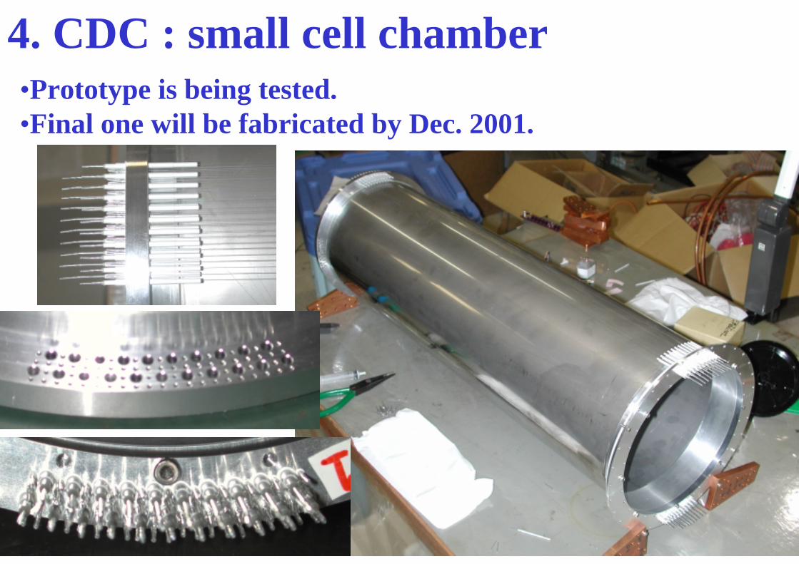
4. CDC : small cell chamber•Prototype is being tested.•Final one will be fabricated by Dec. 2001.
Top Related