With Clear and Preset - TI
26
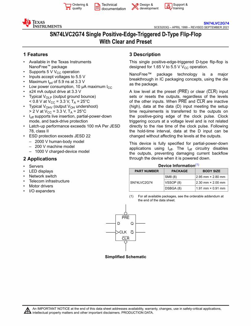
SN74LVC2G74 Single Positive-Edge-Triggered D-Type Flip-Flop With Clear and Preset 1 Features • Available in the Texas Instruments NanoFree ™ package • Supports 5 V V CC operation • Inputs accept voltages to 5.5 V • Maximum t pd of 5.9 ns at 3.3 V • Low power consumption, 10 μA maximum I CC • ±24 mA output drive at 3.3 V • Typical V OLP (output ground bounce) < 0.8 V at V CC = 3.3 V, T A = 25°C • Typical V OHV (output V OH undershoot) > 2 V at V CC = 3.3 V, T A = 25°C • I off supports live insertion, partial-power-down mode, and back-drive protection • Latch-up performance exceeds 100 mA Per JESD 78, class II • ESD protection exceeds JESD 22 – 2000 V human-body model – 200 V machine model – 1000 V charged-device model 2 Applications • Servers • LED displays • Network switch • Telecom infrastructure • Motor drivers • I/O expanders 3 Description This single positive-edge-triggered D-type flip-flop is designed for 1.65 V to 5.5 V V CC operation. NanoFree™ package technology is a major breakthrough in IC packaging concepts, using the die as the package. A low level at the preset ( PRE) or clear ( CLR) input sets or resets the outputs, regardless of the levels of the other inputs. When PRE and CLR are inactive (high), data at the data (D) input meeting the setup time requirements is transferred to the outputs on the positive-going edge of the clock pulse. Clock triggering occurs at a voltage level and is not related directly to the rise time of the clock pulse. Following the hold-time interval, data at the D input can be changed without affecting the levels at the outputs. This device is fully specified for partial-power-down applications using I off . The I off circuitry disables the outputs, preventing damaging current backflow through the device when it is powered down. Device Information (1) PART NUMBER PACKAGE BODY SIZE SN74LVC2G74 SM8 (8) 2.95 mm × 2.80 mm VSSOP (8) 2.30 mm × 2.00 mm DSBGA (8) 1.91 mm × 0.91 mm (1) For all available packages, see the orderable addendum at the end of the data sheet. D Q Q CLR PRE CLK Simplified Schematic SN74LVC2G74 SCES203Q – APRIL 1999 – REVISED SEPTEMBER 2021 An IMPORTANT NOTICE at the end of this data sheet addresses availability, warranty, changes, use in safety-critical applications, intellectual property matters and other important disclaimers. PRODUCTION DATA.
Transcript of With Clear and Preset - TI
SN74LVC2G74 Single Positive-Edge-Triggered D-Type Flip-FlopWith Clear and Preset
1 Features• Available in the Texas Instruments
NanoFree™ package• Supports 5 V VCC operation• Inputs accept voltages to 5.5 V• Maximum tpd of 5.9 ns at 3.3 V• Low power consumption, 10 μA maximum ICC• ±24 mA output drive at 3.3 V• Typical VOLP (output ground bounce)
< 0.8 V at VCC = 3.3 V, TA = 25°C• Typical VOHV (output VOH undershoot)
> 2 V at VCC = 3.3 V, TA = 25°C• Ioff supports live insertion, partial-power-down
mode, and back-drive protection• Latch-up performance exceeds 100 mA Per JESD
78, class II• ESD protection exceeds JESD 22
– 2000 V human-body model– 200 V machine model– 1000 V charged-device model
2 Applications• Servers• LED displays• Network switch• Telecom infrastructure• Motor drivers• I/O expanders
3 DescriptionThis single positive-edge-triggered D-type flip-flop is designed for 1.65 V to 5.5 V VCC operation.
NanoFree™ package technology is a major breakthrough in IC packaging concepts, using the die as the package.
A low level at the preset (PRE) or clear (CLR) input sets or resets the outputs, regardless of the levels of the other inputs. When PRE and CLR are inactive (high), data at the data (D) input meeting the setup time requirements is transferred to the outputs on the positive-going edge of the clock pulse. Clock triggering occurs at a voltage level and is not related directly to the rise time of the clock pulse. Following the hold-time interval, data at the D input can be changed without affecting the levels at the outputs.
This device is fully specified for partial-power-down applications using Ioff. The Ioff circuitry disables the outputs, preventing damaging current backflow through the device when it is powered down.
Device Information(1)
PART NUMBER PACKAGE BODY SIZE
SN74LVC2G74
SM8 (8) 2.95 mm × 2.80 mm
VSSOP (8) 2.30 mm × 2.00 mm
DSBGA (8) 1.91 mm × 0.91 mm
(1) For all available packages, see the orderable addendum at the end of the data sheet.
D Q
Q
CLR
PRE
CLK
Simplified Schematic
SN74LVC2G74SCES203Q – APRIL 1999 – REVISED SEPTEMBER 2021
An IMPORTANT NOTICE at the end of this data sheet addresses availability, warranty, changes, use in safety-critical applications, intellectual property matters and other important disclaimers. PRODUCTION DATA.
Table of Contents1 Features............................................................................12 Applications..................................................................... 13 Description.......................................................................14 Revision History.............................................................. 25 Pin Configuration and Functions...................................36 Specifications.................................................................. 4
6.1 Absolute Maximum Ratings........................................ 46.2 ESD Ratings............................................................... 46.3 Recommended Operating Conditions.........................56.4 Thermal Information....................................................56.5 Electrical Characteristics.............................................66.6 Timing Requirements, –40°C to +85°C.......................66.7 Timing Requirements, –40°C to +125°C.....................66.8 Switching Characteristics, –40°C to +85°C.................76.9 Switching Characteristics, –40°C to +125°C...............76.10 Operating Characteristics......................................... 76.11 Typical Characteristics.............................................. 7
7 Parameter Measurement Information............................ 88 Detailed Description........................................................9
8.1 Overview..................................................................... 98.2 Functional Block Diagram........................................... 98.3 Feature Description.....................................................98.4 Device Functional Modes............................................9
9 Application and Implementation.................................. 109.1 Application Information............................................. 109.2 Typical Power Button Circuit..................................... 10
10 Power Supply Recommendations..............................1111 Layout...........................................................................12
11.1 Layout Guidelines................................................... 1211.2 Layout Example...................................................... 12
12 Device and Documentation Support..........................1312.1 Receiving Notification of Documentation Updates..1312.2 Support Resources................................................. 1312.3 Trademarks.............................................................1312.4 Electrostatic Discharge Caution..............................1312.5 Glossary..................................................................13
13 Mechanical, Packaging, and Orderable Information.................................................................... 13
4 Revision HistoryNOTE: Page numbers for previous revisions may differ from page numbers in the current version.
Changes from Revision P (July 2016) to Revision Q (September 2021) Page• Updated the numbering format for tables, figures, and cross-references throughout the document..................1• Updated the Application and Information section............................................................................................. 10• Updated the Device Power Button Circuit figure in the Typical Power Button Circuit section.......................... 10
Changes from Revision O (January 2015) to Revision P (July 2016) Page• Changed SSOP to SM8 in Device Information table.......................................................................................... 1• Updated pinout images to new format................................................................................................................ 3• Added pin number for DSBGA package in Pin Functions table..........................................................................3• Changed 6 PINS to 8 PINS in Thermal Information table...................................................................................5• Changed 23 to 2.3 for tsu data in Timing Requirements, –40°C to +125°C ....................................................... 6
Changes from Revision N (July 2013) to Revision O (January 2015) Page• Added Applications, Device Information table, Pin Functions table, ESD Ratings table, Thermal Information
table, Typical Characteristics, Feature Description section, Device Functional Modes, Application and Implementation section, Power Supply Recommendations section, Layout section, Device and Documentation Support section, and Mechanical, Packaging, and Orderable Information section................... 1
Changes from Revision M (February 2007) to Revision N (July 2013) Page• Changed Ioff description in Features...................................................................................................................1• Added parameter values for –40 to +125°C temperature ratings in Electrical Characteristics table.................. 6• Changed Timing Requirements, –40°C to +85°C table...................................................................................... 6• Added Timing Requirements, –40°C to +125°C table........................................................................................ 6• Changed Switching Characteristics, –40°C to +85°C table................................................................................ 7• Added Switching Characteristics, –40°C to +125°C table.................................................................................. 7
SN74LVC2G74SCES203Q – APRIL 1999 – REVISED SEPTEMBER 2021 www.ti.com
2 Submit Document Feedback Copyright © 2021 Texas Instruments Incorporated
Product Folder Links: SN74LVC2G74
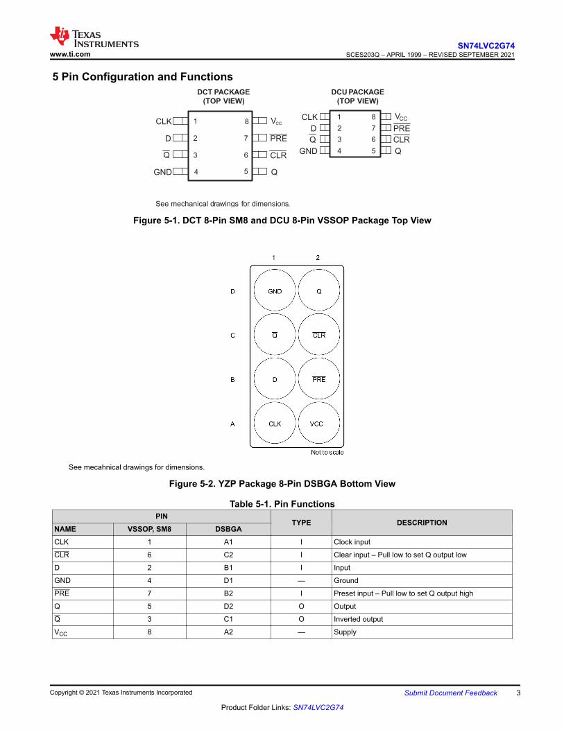
5 Pin Configuration and FunctionsDCT PACKAGE
(TOP VIEW)
CLK 1 8 VCC
D 2 7 PRE
Q 3 6 CLR
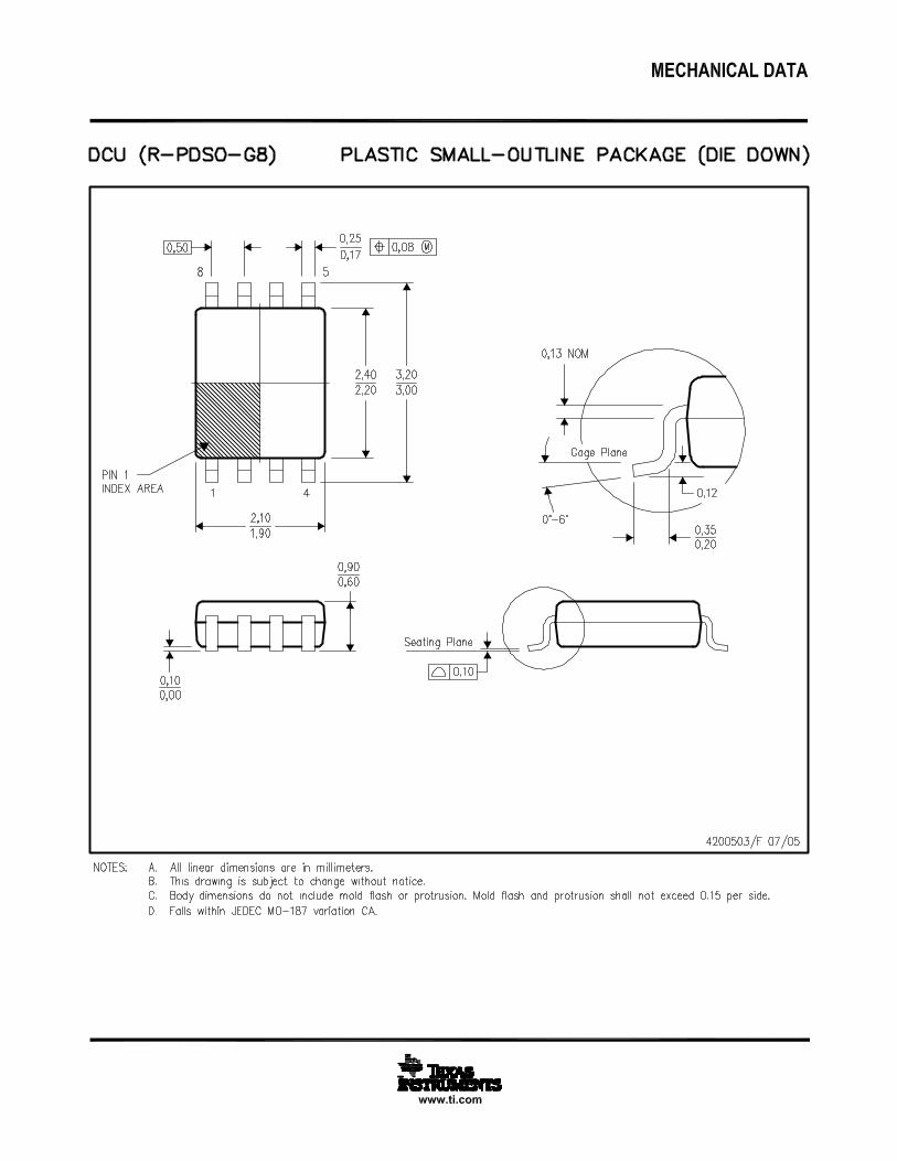
DCU PACKAGE
(TOP VIEW)
CLK 1 8 VCC
D 2 7 PRE
Q 3 6 CLR
GND 4 5 Q
GND 4 5 Q
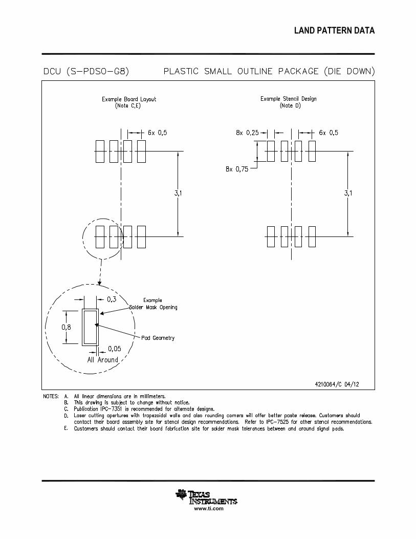
See mechanical drawings for dimensions.
Figure 5-1. DCT 8-Pin SM8 and DCU 8-Pin VSSOP Package Top View
See mecahnical drawings for dimensions.
Figure 5-2. YZP Package 8-Pin DSBGA Bottom View
Table 5-1. Pin FunctionsPIN
TYPE DESCRIPTIONNAME VSSOP, SM8 DSBGACLK 1 A1 I Clock input
CLR 6 C2 I Clear input – Pull low to set Q output low
D 2 B1 I Input
GND 4 D1 — Ground
PRE 7 B2 I Preset input – Pull low to set Q output high
Q 5 D2 O Output
Q 3 C1 O Inverted output
VCC 8 A2 — Supply
www.ti.comSN74LVC2G74
SCES203Q – APRIL 1999 – REVISED SEPTEMBER 2021
Copyright © 2021 Texas Instruments Incorporated Submit Document Feedback 3
Product Folder Links: SN74LVC2G74
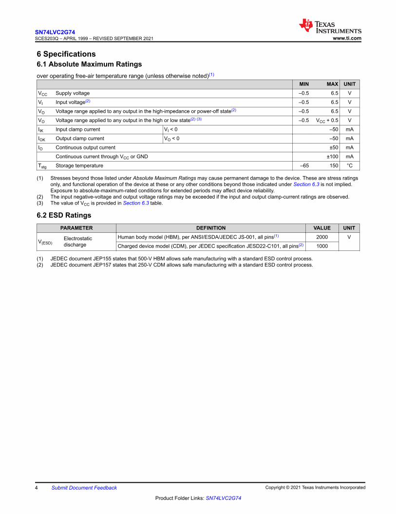
6 Specifications6.1 Absolute Maximum Ratingsover operating free-air temperature range (unless otherwise noted)(1)
MIN MAX UNITVCC Supply voltage –0.5 6.5 V
VI Input voltage(2) –0.5 6.5 V
VO Voltage range applied to any output in the high-impedance or power-off state(2) –0.5 6.5 V
VO Voltage range applied to any output in the high or low state(2) (3) –0.5 VCC + 0.5 V
IIK Input clamp current VI < 0 –50 mA
IOK Output clamp current VO < 0 –50 mA
IO Continuous output current ±50 mA
Continuous current through VCC or GND ±100 mA
Tstg Storage temperature –65 150 °C
(1) Stresses beyond those listed under Absolute Maximum Ratings may cause permanent damage to the device. These are stress ratings only, and functional operation of the device at these or any other conditions beyond those indicated under Section 6.3 is not implied. Exposure to absolute-maximum-rated conditions for extended periods may affect device reliability.
(2) The input negative-voltage and output voltage ratings may be exceeded if the input and output clamp-current ratings are observed.(3) The value of VCC is provided in Section 6.3 table.
6.2 ESD RatingsPARAMETER DEFINITION VALUE UNIT
V(ESD)Electrostatic discharge
Human body model (HBM), per ANSI/ESDA/JEDEC JS-001, all pins(1) 2000 V
Charged device model (CDM), per JEDEC specification JESD22-C101, all pins(2) 1000
(1) JEDEC document JEP155 states that 500-V HBM allows safe manufacturing with a standard ESD control process.(2) JEDEC document JEP157 states that 250-V CDM allows safe manufacturing with a standard ESD control process.
SN74LVC2G74SCES203Q – APRIL 1999 – REVISED SEPTEMBER 2021 www.ti.com
4 Submit Document Feedback Copyright © 2021 Texas Instruments Incorporated
Product Folder Links: SN74LVC2G74
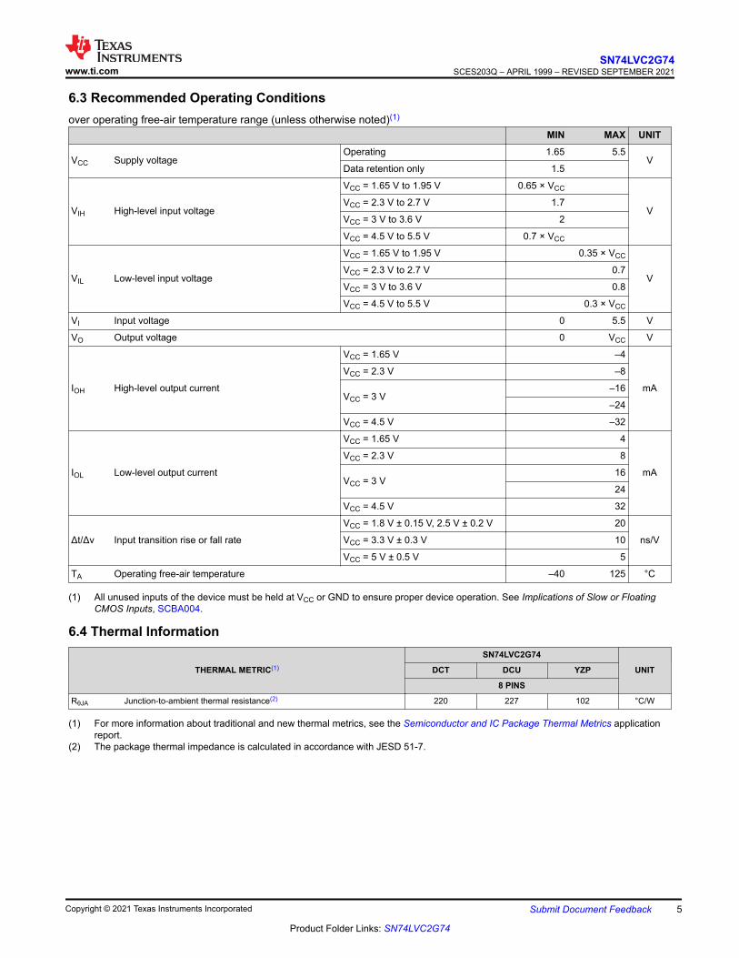
6.3 Recommended Operating Conditionsover operating free-air temperature range (unless otherwise noted)(1)
MIN MAX UNIT
VCC Supply voltageOperating 1.65 5.5
VData retention only 1.5
VIH High-level input voltage
VCC = 1.65 V to 1.95 V 0.65 × VCC
VVCC = 2.3 V to 2.7 V 1.7
VCC = 3 V to 3.6 V 2
VCC = 4.5 V to 5.5 V 0.7 × VCC
VIL Low-level input voltage
VCC = 1.65 V to 1.95 V 0.35 × VCC
VVCC = 2.3 V to 2.7 V 0.7
VCC = 3 V to 3.6 V 0.8
VCC = 4.5 V to 5.5 V 0.3 × VCC
VI Input voltage 0 5.5 V
VO Output voltage 0 VCC V
IOH High-level output current
VCC = 1.65 V –4
mA
VCC = 2.3 V –8
VCC = 3 V–16
–24
VCC = 4.5 V –32
IOL Low-level output current
VCC = 1.65 V 4
mA
VCC = 2.3 V 8
VCC = 3 V16
24
VCC = 4.5 V 32
Δt/Δv Input transition rise or fall rate
VCC = 1.8 V ± 0.15 V, 2.5 V ± 0.2 V 20
ns/VVCC = 3.3 V ± 0.3 V 10
VCC = 5 V ± 0.5 V 5
TA Operating free-air temperature –40 125 °C
(1) All unused inputs of the device must be held at VCC or GND to ensure proper device operation. See Implications of Slow or Floating CMOS Inputs, SCBA004.
6.4 Thermal Information
THERMAL METRIC(1)
SN74LVC2G74
UNITDCT DCU YZP
8 PINS
RθJA Junction-to-ambient thermal resistance(2) 220 227 102 °C/W
(1) For more information about traditional and new thermal metrics, see the Semiconductor and IC Package Thermal Metrics application report.
(2) The package thermal impedance is calculated in accordance with JESD 51-7.
www.ti.comSN74LVC2G74
SCES203Q – APRIL 1999 – REVISED SEPTEMBER 2021
Copyright © 2021 Texas Instruments Incorporated Submit Document Feedback 5
Product Folder Links: SN74LVC2G74
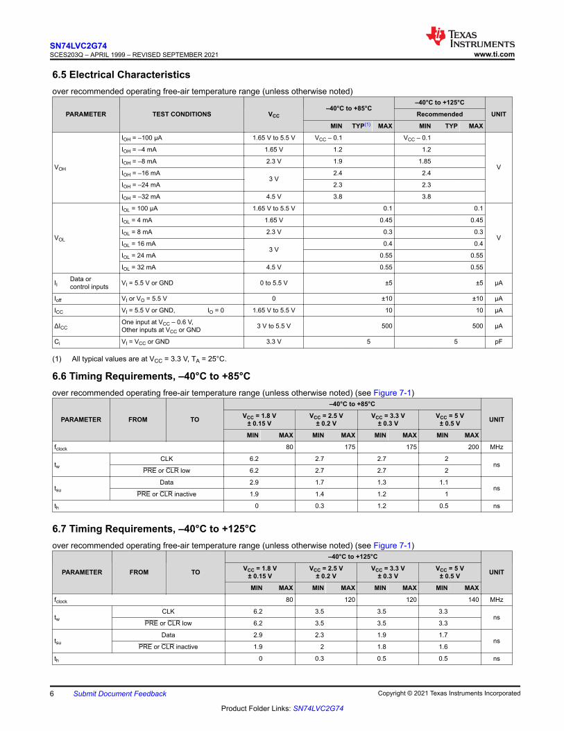
6.5 Electrical Characteristicsover recommended operating free-air temperature range (unless otherwise noted)
PARAMETER TEST CONDITIONS VCC–40°C to +85°C
–40°C to +125°C
UNITRecommended
MIN TYP(1) MAX MIN TYP MAX
VOH
IOH = –100 μA 1.65 V to 5.5 V VCC – 0.1 VCC – 0.1
V
IOH = –4 mA 1.65 V 1.2 1.2
IOH = –8 mA 2.3 V 1.9 1.85
IOH = –16 mA3 V
2.4 2.4
IOH = –24 mA 2.3 2.3
IOH = –32 mA 4.5 V 3.8 3.8
VOL
IOL = 100 μA 1.65 V to 5.5 V 0.1 0.1
V
IOL = 4 mA 1.65 V 0.45 0.45
IOL = 8 mA 2.3 V 0.3 0.3
IOL = 16 mA3 V
0.4 0.4
IOL = 24 mA 0.55 0.55
IOL = 32 mA 4.5 V 0.55 0.55
IIData orcontrol inputs VI = 5.5 V or GND 0 to 5.5 V ±5 ±5 μA
Ioff VI or VO = 5.5 V 0 ±10 ±10 μA
ICC VI = 5.5 V or GND, IO = 0 1.65 V to 5.5 V 10 10 μA
ΔICCOne input at VCC – 0.6 V,Other inputs at VCC or GND 3 V to 5.5 V 500 500 μA
Ci VI = VCC or GND 3.3 V 5 5 pF
(1) All typical values are at VCC = 3.3 V, TA = 25°C.
6.6 Timing Requirements, –40°C to +85°Cover recommended operating free-air temperature range (unless otherwise noted) (see Figure 7-1)
PARAMETER FROM TO
–40°C to +85°C
UNITVCC = 1.8 V± 0.15 V
VCC = 2.5 V± 0.2 V
VCC = 3.3 V± 0.3 V
VCC = 5 V± 0.5 V
MIN MAX MIN MAX MIN MAX MIN MAX
fclock 80 175 175 200 MHz
twCLK 6.2 2.7 2.7 2
nsPRE or CLR low 6.2 2.7 2.7 2
tsuData 2.9 1.7 1.3 1.1
nsPRE or CLR inactive 1.9 1.4 1.2 1
th 0 0.3 1.2 0.5 ns
6.7 Timing Requirements, –40°C to +125°Cover recommended operating free-air temperature range (unless otherwise noted) (see Figure 7-1)
PARAMETER FROM TO
–40°C to +125°C
UNITVCC = 1.8 V± 0.15 V
VCC = 2.5 V± 0.2 V
VCC = 3.3 V± 0.3 V
VCC = 5 V± 0.5 V
MIN MAX MIN MAX MIN MAX MIN MAX
fclock 80 120 120 140 MHz
twCLK 6.2 3.5 3.5 3.3
nsPRE or CLR low 6.2 3.5 3.5 3.3
tsuData 2.9 2.3 1.9 1.7
nsPRE or CLR inactive 1.9 2 1.8 1.6
th 0 0.3 0.5 0.5 ns
SN74LVC2G74SCES203Q – APRIL 1999 – REVISED SEPTEMBER 2021 www.ti.com
6 Submit Document Feedback Copyright © 2021 Texas Instruments Incorporated
Product Folder Links: SN74LVC2G74
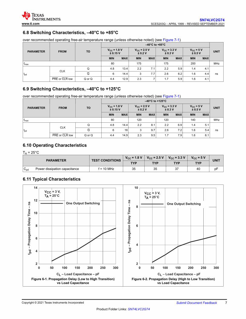
6.8 Switching Characteristics, –40°C to +85°Cover recommended operating free-air temperature range (unless otherwise noted) (see Figure 7-1)
PARAMETER FROM TO
–40°C to +85°C
UNITVCC = 1.8 V± 0.15 V
VCC = 2.5 V± 0.2 V
VCC = 3.3 V± 0.3 V
VCC = 5 V± 0.5 V
MIN MAX MIN MAX MIN MAX MIN MAX
fmax 80 175 175 200 MHz
tpdCLK
Q 4.8 13.4 2.2 7.1 2.2 5.9 1.4 4.1
nsQ 6 14.4 3 7.7 2.6 6.2 1.6 4.4
PRE or CLR low Q or Q 4.4 12.9 2.3 7 1.7 5.9 1.6 4.1
6.9 Switching Characteristics, –40°C to +125°Cover recommended operating free-air temperature range (unless otherwise noted) (see Figure 7-1)
PARAMETER FROM TO
–40°C to +125°C
UNITVCC = 1.8 V± 0.15 V
VCC = 2.5 V± 0.2 V
VCC = 3.3 V± 0.3 V
VCC = 5 V± 0.5 V
MIN MAX MIN MAX MIN MAX MIN MAX
fmax 80 120 120 140 MHz
tpdCLK
Q 4.8 14.4 2.2 8.1 2.2 6.9 1.4 5.1
nsQ 6 16 3 9.7 2.6 7.2 1.6 5.4
PRE or CLR low Q or Q 4.4 14.9 2.3 9.5 1.7 7.9 1.6 6.1
6.10 Operating CharacteristicsTA = 25°C
PARAMETER TEST CONDITIONSVCC = 1.8 V VCC = 2.5 V VCC = 3.3 V VCC = 5 V
UNITTYP TYP TYP TYP
Cpd Power dissipation capacitance f = 10 MHz 35 35 37 40 pF
6.11 Typical Characteristics
2
4
6
8
10
12
14
0 50 100 150 200 250 300
CL – Load Capacitance – pF
VCC = 3 V,
TA = 25°C
One Output Switching
t–
Pro
pag
ati
on
Dela
yT
ime
–n
sp
d
Figure 6-1. Propagation Delay (Low to High Transition)vs Load Capacitance
2
4
6
8
10
0 50 100 150 200 250 300
CL – Load Capacitance – pF
t–
Pro
pag
ati
on
Dela
yT
ime
–n
sp
d
VCC = 3 V,
TA = 25°C
One Output Switching
Figure 6-2. Propagation Delay (High to Low Transition)vs Load Capacitance
www.ti.comSN74LVC2G74
SCES203Q – APRIL 1999 – REVISED SEPTEMBER 2021
Copyright © 2021 Texas Instruments Incorporated Submit Document Feedback 7
Product Folder Links: SN74LVC2G74
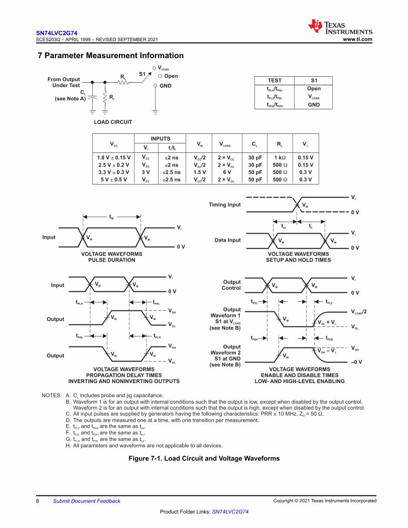
7 Parameter Measurement Information
thtsu
From OutputUnder Test
C
(see Note A)L
LOAD CIRCUIT
S1
VLOAD
Open
GND
RL
Data Input
Timing Input
0 V
0 V0 V
tW
Input
0 VInput
OutputWaveform 1
S1 at V
(see Note B)LOAD
OutputWaveform 2
S1 at GND(see Note B)
VOL
VOH
0 V
»0 V
Output
Output
TEST S1
t /tPLH PHL Open
OutputControl
VM
VM VM
VM
VM
1.8 V 0.15 V±
2.5 V 0.2 V±
3.3 V 0.3 V±
5 V 0.5 V±
1 kW
500 W
500 W
500 W
VCC RL
2 × VCC
2 × VCC
6 V
2 × VCC
VLOAD CL
30 pF
30 pF
50 pF
50 pF
0.15 V
0.15 V
0.3 V
0.3 V
VD
3 V
VI
VCC/2
VCC/2
1.5 V
VCC/2
VM
£2 ns
£2 ns
£2.5 ns
£2.5 ns
INPUTS
RL
t /tr f
VCC
VCC
VCC
VLOADt /tPLZ PZL
GNDt /tPHZ PZH
VOLTAGE WAVEFORMSENABLE AND DISABLE TIMES
LOW- AND HIGH-LEVEL ENABLING
VOLTAGE WAVEFORMSPROPAGATION DELAY TIMES
INVERTING AND NONINVERTING OUTPUTS
NOTES: A. C includes probe and jig capacitance.
B. Waveform 1 is for an output with internal conditions such that the output is low, except when disabled by the output control.Waveform 2 is for an output with internal conditions such that the output is high, except when disabled by the output control.
C. All input pulses are supplied by generators having the following characteristics: PRR 10 MHz, Z = 50 .
D. The outputs are measured one at a time, with one transition per measurement.E. t and t are the same as t .
F. t and t are the same as t .
G. t and t are the same as t .
H. All parameters and waveforms are not applicable to all devices.
L
O
PLZ PHZ dis
PZL PZH en
PLH PHL pd
£ W
VOLTAGE WAVEFORMSPULSE DURATION
VOLTAGE WAVEFORMSSETUP AND HOLD TIMES
VI
VI
VI
VM
VM
V /2LOAD
tPZL tPLZ
tPHZtPZH
V – VOH D
V + VOL D
VM
VM VM
VM
VOL
VOH
VI
VI
VOH
VOL
VM
VM
VM
VM
tPLH tPHL
tPLHtPHL
Figure 7-1. Load Circuit and Voltage Waveforms
SN74LVC2G74SCES203Q – APRIL 1999 – REVISED SEPTEMBER 2021 www.ti.com
8 Submit Document Feedback Copyright © 2021 Texas Instruments Incorporated
Product Folder Links: SN74LVC2G74
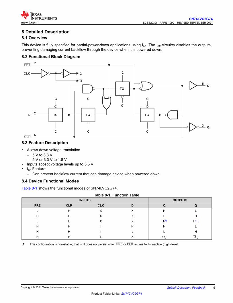
8 Detailed Description8.1 OverviewThis device is fully specified for partial-power-down applications using Ioff. The Ioff circuitry disables the outputs, preventing damaging current backflow through the device when it is powered down.
8.2 Functional Block Diagram
TG
C
C
TG
C
C
TG
C
C
C
TG
C
C
PRE
CLK
D
CLR
Q
Q
C
7
2
6
5
3
1
8.3 Feature Description• Allows down voltage translation
– 5 V to 3.3 V– 5 V or 3.3 V to 1.8 V
• Inputs accept voltage levels up to 5.5 V• Ioff Feature
– Can prevent backflow current that can damage device when powered down.
8.4 Device Functional ModesTable 8-1 shows the functional modes of SN74LVC2G74.
Table 8-1. Function TableINPUTS OUTPUTS
PRE CLR CLK D Q QL H X X H LH L X X L HL L X X H(1) H(1)
H H ↑ H H LH H ↑ L L HH H L X Q0 Q 0
(1) This configuration is non-stable; that is, it does not persist when PRE or CLR returns to its inactive (high) level.
www.ti.comSN74LVC2G74
SCES203Q – APRIL 1999 – REVISED SEPTEMBER 2021
Copyright © 2021 Texas Instruments Incorporated Submit Document Feedback 9
Product Folder Links: SN74LVC2G74
9 Application and ImplementationNote
Information in the following applications sections is not part of the TI component specification, and TI does not warrant its accuracy or completeness. TI’s customers are responsible for determining suitability of components for their purposes, as well as validating and testing their design implementation to confirm system functionality.
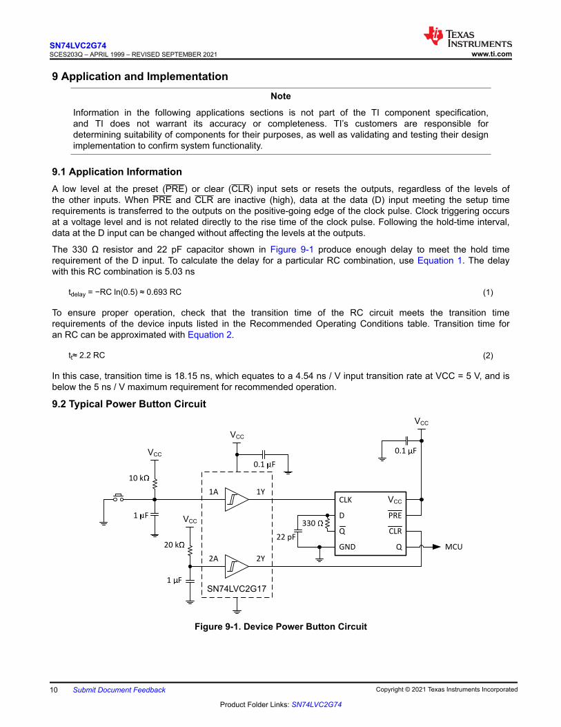
9.1 Application InformationA low level at the preset (PRE) or clear (CLR) input sets or resets the outputs, regardless of the levels of the other inputs. When PRE and CLR are inactive (high), data at the data (D) input meeting the setup time requirements is transferred to the outputs on the positive-going edge of the clock pulse. Clock triggering occurs at a voltage level and is not related directly to the rise time of the clock pulse. Following the hold-time interval, data at the D input can be changed without affecting the levels at the outputs.
The 330 Ω resistor and 22 pF capacitor shown in Figure 9-1 produce enough delay to meet the hold time requirement of the D input. To calculate the delay for a particular RC combination, use Equation 1. The delay with this RC combination is 5.03 ns
tdelay = −RC ln(0.5) ≈ 0.693 RC (1)
To ensure proper operation, check that the transition time of the RC circuit meets the transition time requirements of the device inputs listed in the Recommended Operating Conditions table. Transition time for an RC can be approximated with Equation 2.
tt≈ 2.2 RC (2)
In this case, transition time is 18.15 ns, which equates to a 4.54 ns / V input transition rate at VCC = 5 V, and is below the 5 ns / V maximum requirement for recommended operation.
9.2 Typical Power Button Circuit
SN74LVC2G17
1 �F
10 k�
VCC
1A 1YCLK
D
Q
GND
VCC
PRE
CLR
Q
VCC
0.1 �F
MCU
22 pF
330 �
2A 2Y
VCC
20 k�
1 �F
0.1 �F
VCC
Figure 9-1. Device Power Button Circuit
SN74LVC2G74SCES203Q – APRIL 1999 – REVISED SEPTEMBER 2021 www.ti.com
10 Submit Document Feedback Copyright © 2021 Texas Instruments Incorporated
Product Folder Links: SN74LVC2G74
9.2.1 Design Requirements
This device uses CMOS technology and has balanced output drive. Care should be taken to avoid bus contention because it can drive currents that would exceed maximum limits. Outputs can be combined to produce higher drive but the high drive will also create faster edges into light loads so routing and load conditions should be considered to prevent ringing.
9.2.2 Detailed Design Procedure
1. Recommended Input Conditions:• For rise time and fall time specifications, see (Δt/ΔV) in the Recommended Operating Conditions table.• For specified high and low levels, see (VIH and VIL) in the Recommended Operating Conditions table.• Inputs are overvoltage tolerant allowing them to go as high as 5.5 V at any valid VCC
2. Recommend Output Conditions:• Load currents should not exceed 50 mA per output and 100 mA total for the part.• Series resistors on the output may be used if the user desires to slow the output edge signal or limit the
output current.
9.2.3 Application Curves
–100
–80
–60
–40
–20
0
20
40
60
–1 –0.5 0.0 0.5 1.0 1.5 2.0 2.5 3.0 3.5 4.0
TA = 25°C, VCC = 3 V,
VIH = 3 V, VIL = 0 V,
All Outputs Switching
VOH – V
I OH
–m
A
Figure 9-2. Output Current Drivevs HIGH-Level Output Voltage
VOL – V
–20
0
20
40
60
80
100
–0.2 0.0 0.2 0.4 0.6 0.8 1.0 1.2 1.4 1.6
TA = 25°C, VCC = 3 V,
VIH = 3 V, VIL = 0 V,
All Outputs SwitchingI O
L–
mA
Figure 9-3. Output Current Drivevs LOW-Level Output Voltage
10 Power Supply RecommendationsThe power supply can be any voltage between the minimum and maximum supply voltage rating located in the Recommended Operating Conditions table. Each VCC terminal should have a good bypass capacitor to prevent power disturbance. For devices with a single supply, a 0.1-μF capacitor is recommended and if there are multiple VCC terminals then .01-μF or .022-μF capacitors are recommended for each power terminal. It is acceptable to parallel multiple bypass caps to reject different frequencies of noise. The 0.1-μF and 1-μF capacitors are commonly used in parallel. The bypass capacitor should be installed as close to the power terminal as possible for best results.
www.ti.comSN74LVC2G74
SCES203Q – APRIL 1999 – REVISED SEPTEMBER 2021
Copyright © 2021 Texas Instruments Incorporated Submit Document Feedback 11
Product Folder Links: SN74LVC2G74
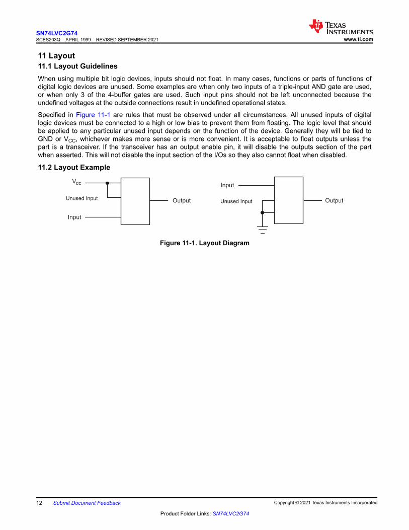
11 Layout11.1 Layout GuidelinesWhen using multiple bit logic devices, inputs should not float. In many cases, functions or parts of functions of digital logic devices are unused. Some examples are when only two inputs of a triple-input AND gate are used, or when only 3 of the 4-buffer gates are used. Such input pins should not be left unconnected because the undefined voltages at the outside connections result in undefined operational states.
Specified in Figure 11-1 are rules that must be observed under all circumstances. All unused inputs of digital logic devices must be connected to a high or low bias to prevent them from floating. The logic level that should be applied to any particular unused input depends on the function of the device. Generally they will be tied to GND or VCC, whichever makes more sense or is more convenient. It is acceptable to float outputs unless the part is a transceiver. If the transceiver has an output enable pin, it will disable the outputs section of the part when asserted. This will not disable the input section of the I/Os so they also cannot float when disabled.
11.2 Layout Example
Vcc
Unused Input
Input
Output
Input
Unused Input Output
Figure 11-1. Layout Diagram
SN74LVC2G74SCES203Q – APRIL 1999 – REVISED SEPTEMBER 2021 www.ti.com
12 Submit Document Feedback Copyright © 2021 Texas Instruments Incorporated
Product Folder Links: SN74LVC2G74
12 Device and Documentation Support12.1 Receiving Notification of Documentation UpdatesTo receive notification of documentation updates, navigate to the device product folder on ti.com. Click on Subscribe to updates to register and receive a weekly digest of any product information that has changed. For change details, review the revision history included in any revised document.
12.2 Support ResourcesTI E2E™ support forums are an engineer's go-to source for fast, verified answers and design help — straight from the experts. Search existing answers or ask your own question to get the quick design help you need.
Linked content is provided "AS IS" by the respective contributors. They do not constitute TI specifications and do not necessarily reflect TI's views; see TI's Terms of Use.
12.3 TrademarksNanoFree™ is a trademark of Texas Instruments.TI E2E™ is a trademark of Texas Instruments.All trademarks are the property of their respective owners.12.4 Electrostatic Discharge Caution
This integrated circuit can be damaged by ESD. Texas Instruments recommends that all integrated circuits be handled with appropriate precautions. Failure to observe proper handling and installation procedures can cause damage.ESD damage can range from subtle performance degradation to complete device failure. Precision integrated circuits may be more susceptible to damage because very small parametric changes could cause the device not to meet its published specifications.
12.5 GlossaryTI Glossary This glossary lists and explains terms, acronyms, and definitions.
13 Mechanical, Packaging, and Orderable InformationThe following pages include mechanical packaging and orderable information. This information is the most current data available for the designated devices. This data is subject to change without notice and revision of this document. For browser based versions of this data sheet, refer to the left hand navigation.
www.ti.comSN74LVC2G74
SCES203Q – APRIL 1999 – REVISED SEPTEMBER 2021
Copyright © 2021 Texas Instruments Incorporated Submit Document Feedback 13
Product Folder Links: SN74LVC2G74
PACKAGE OPTION ADDENDUM
www.ti.com 26-Jul-2021
Addendum-Page 1
PACKAGING INFORMATION
Orderable Device Status(1)
Package Type PackageDrawing
Pins PackageQty
Eco Plan(2)
Lead finish/Ball material
(6)
MSL Peak Temp(3)
Op Temp (°C) Device Marking(4/5)
Samples
SN74LVC2G74DCT3 ACTIVE SM8 DCT 8 3000 RoHS &Non-Green
SNBI Level-1-260C-UNLIM -40 to 125 C74Z
SN74LVC2G74DCTR ACTIVE SM8 DCT 8 3000 RoHS & Green NIPDAU Level-1-260C-UNLIM -40 to 125 C74Z
SN74LVC2G74DCTRE4 ACTIVE SM8 DCT 8 3000 RoHS & Green NIPDAU Level-1-260C-UNLIM -40 to 125 C74Z
SN74LVC2G74DCTRE6 ACTIVE SM8 DCT 8 3000 RoHS &Non-Green
SNBI Level-1-260C-UNLIM -40 to 125 C74Z
SN74LVC2G74DCTRG4 ACTIVE SM8 DCT 8 3000 RoHS & Green NIPDAU Level-1-260C-UNLIM -40 to 125 C74Z
SN74LVC2G74DCUR ACTIVE VSSOP DCU 8 3000 RoHS & Green NIPDAU | SN Level-1-260C-UNLIM -40 to 125 (74, C74J, C74Q, C 74R)CZ
SN74LVC2G74DCURE4 ACTIVE VSSOP DCU 8 3000 RoHS & Green NIPDAU Level-1-260C-UNLIM -40 to 125 C74R
SN74LVC2G74DCURG4 ACTIVE VSSOP DCU 8 3000 RoHS & Green NIPDAU Level-1-260C-UNLIM -40 to 125 C74R
SN74LVC2G74DCUT ACTIVE VSSOP DCU 8 250 RoHS & Green NIPDAU | SN Level-1-260C-UNLIM -40 to 125 (C74J, C74Q, C74R)
SN74LVC2G74DCUTE4 ACTIVE VSSOP DCU 8 250 RoHS & Green NIPDAU Level-1-260C-UNLIM -40 to 125 C74R
SN74LVC2G74DCUTG4 ACTIVE VSSOP DCU 8 250 RoHS & Green NIPDAU Level-1-260C-UNLIM -40 to 125 C74R
SN74LVC2G74YZPR ACTIVE DSBGA YZP 8 3000 RoHS & Green SNAGCU Level-1-260C-UNLIM -40 to 85 CPN
(1) The marketing status values are defined as follows:ACTIVE: Product device recommended for new designs.LIFEBUY: TI has announced that the device will be discontinued, and a lifetime-buy period is in effect.NRND: Not recommended for new designs. Device is in production to support existing customers, but TI does not recommend using this part in a new design.PREVIEW: Device has been announced but is not in production. Samples may or may not be available.OBSOLETE: TI has discontinued the production of the device.
(2) RoHS: TI defines "RoHS" to mean semiconductor products that are compliant with the current EU RoHS requirements for all 10 RoHS substances, including the requirement that RoHS substancedo not exceed 0.1% by weight in homogeneous materials. Where designed to be soldered at high temperatures, "RoHS" products are suitable for use in specified lead-free processes. TI mayreference these types of products as "Pb-Free".RoHS Exempt: TI defines "RoHS Exempt" to mean products that contain lead but are compliant with EU RoHS pursuant to a specific EU RoHS exemption.
PACKAGE OPTION ADDENDUM
www.ti.com 26-Jul-2021
Addendum-Page 2
Green: TI defines "Green" to mean the content of Chlorine (Cl) and Bromine (Br) based flame retardants meet JS709B low halogen requirements of <=1000ppm threshold. Antimony trioxide basedflame retardants must also meet the <=1000ppm threshold requirement.
(3) MSL, Peak Temp. - The Moisture Sensitivity Level rating according to the JEDEC industry standard classifications, and peak solder temperature.
(4) There may be additional marking, which relates to the logo, the lot trace code information, or the environmental category on the device.
(5) Multiple Device Markings will be inside parentheses. Only one Device Marking contained in parentheses and separated by a "~" will appear on a device. If a line is indented then it is a continuationof the previous line and the two combined represent the entire Device Marking for that device.
(6) Lead finish/Ball material - Orderable Devices may have multiple material finish options. Finish options are separated by a vertical ruled line. Lead finish/Ball material values may wrap to twolines if the finish value exceeds the maximum column width.
Important Information and Disclaimer:The information provided on this page represents TI's knowledge and belief as of the date that it is provided. TI bases its knowledge and belief on informationprovided by third parties, and makes no representation or warranty as to the accuracy of such information. Efforts are underway to better integrate information from third parties. TI has taken andcontinues to take reasonable steps to provide representative and accurate information but may not have conducted destructive testing or chemical analysis on incoming materials and chemicals.TI and TI suppliers consider certain information to be proprietary, and thus CAS numbers and other limited information may not be available for release.
In no event shall TI's liability arising out of such information exceed the total purchase price of the TI part(s) at issue in this document sold by TI to Customer on an annual basis.
OTHER QUALIFIED VERSIONS OF SN74LVC2G74 :
• Automotive : SN74LVC2G74-Q1
• Enhanced Product : SN74LVC2G74-EP
NOTE: Qualified Version Definitions:
• Automotive - Q100 devices qualified for high-reliability automotive applications targeting zero defects
• Enhanced Product - Supports Defense, Aerospace and Medical Applications
TAPE AND REEL INFORMATION
*All dimensions are nominal
Device PackageType
PackageDrawing
Pins SPQ ReelDiameter
(mm)
ReelWidth
W1 (mm)
A0(mm)
B0(mm)
K0(mm)
P1(mm)
W(mm)
Pin1Quadrant
SN74LVC2G74DCT3 SM8 DCT 8 3000 180.0 13.0 3.35 4.5 1.55 4.0 12.0 Q3
SN74LVC2G74DCTR SM8 DCT 8 3000 180.0 13.0 3.35 4.5 1.55 4.0 12.0 Q3
SN74LVC2G74DCTRE6 SM8 DCT 8 3000 180.0 13.0 3.35 4.5 1.55 4.0 12.0 Q3
SN74LVC2G74DCUR VSSOP DCU 8 3000 178.0 9.0 2.25 3.35 1.05 4.0 8.0 Q3
SN74LVC2G74DCUR VSSOP DCU 8 3000 180.0 9.0 2.25 3.4 1.0 4.0 8.0 Q3
SN74LVC2G74DCURG4 VSSOP DCU 8 3000 180.0 8.4 2.25 3.35 1.05 4.0 8.0 Q3
SN74LVC2G74DCUT VSSOP DCU 8 250 178.0 9.0 2.25 3.35 1.05 4.0 8.0 Q3
SN74LVC2G74DCUTG4 VSSOP DCU 8 250 180.0 8.4 2.25 3.35 1.05 4.0 8.0 Q3
SN74LVC2G74YZPR DSBGA YZP 8 3000 178.0 9.2 1.02 2.02 0.63 4.0 8.0 Q1
PACKAGE MATERIALS INFORMATION
www.ti.com 26-Jul-2021
Pack Materials-Page 1
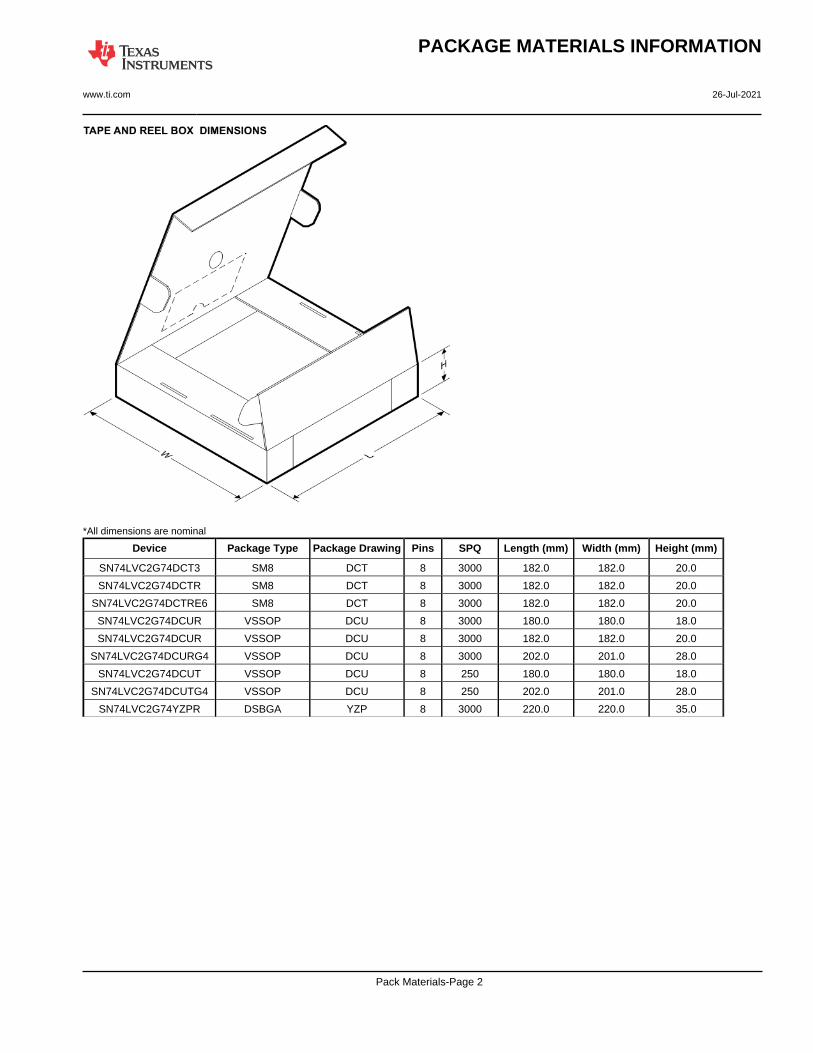
*All dimensions are nominal
Device Package Type Package Drawing Pins SPQ Length (mm) Width (mm) Height (mm)
SN74LVC2G74DCT3 SM8 DCT 8 3000 182.0 182.0 20.0
SN74LVC2G74DCTR SM8 DCT 8 3000 182.0 182.0 20.0
SN74LVC2G74DCTRE6 SM8 DCT 8 3000 182.0 182.0 20.0
SN74LVC2G74DCUR VSSOP DCU 8 3000 180.0 180.0 18.0
SN74LVC2G74DCUR VSSOP DCU 8 3000 182.0 182.0 20.0
SN74LVC2G74DCURG4 VSSOP DCU 8 3000 202.0 201.0 28.0
SN74LVC2G74DCUT VSSOP DCU 8 250 180.0 180.0 18.0
SN74LVC2G74DCUTG4 VSSOP DCU 8 250 202.0 201.0 28.0
SN74LVC2G74YZPR DSBGA YZP 8 3000 220.0 220.0 35.0
PACKAGE MATERIALS INFORMATION
www.ti.com 26-Jul-2021
Pack Materials-Page 2
www.ti.com
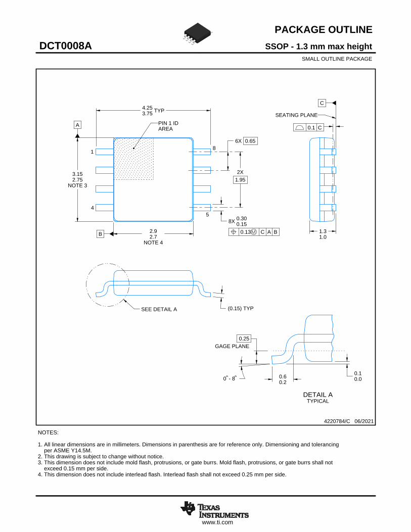
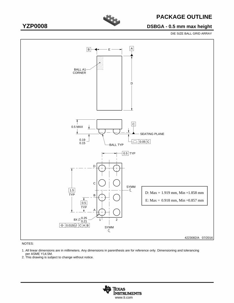
PACKAGE OUTLINE
C4.253.75 TYP
1.31.0
6X 0.65
8X 0.300.15
2X1.95
(0.15) TYP
0 - 80.10.0
0.25GAGE PLANE
0.60.2
A
3.152.75
NOTE 3
B 2.92.7
NOTE 4
4220784/C 06/2021
SSOP - 1.3 mm max heightDCT0008ASMALL OUTLINE PACKAGE
NOTES: 1. All linear dimensions are in millimeters. Dimensions in parenthesis are for reference only. Dimensioning and tolerancing per ASME Y14.5M. 2. This drawing is subject to change without notice. 3. This dimension does not include mold flash, protrusions, or gate burrs. Mold flash, protrusions, or gate burrs shall not exceed 0.15 mm per side. 4. This dimension does not include interlead flash. Interlead flash shall not exceed 0.25 mm per side.
1 8
0.13 C A B
54
PIN 1 IDAREA
SEATING PLANE
0.1 C
SEE DETAIL A
DETAIL ATYPICAL
SCALE 3.500
www.ti.com
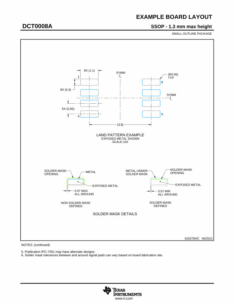
EXAMPLE BOARD LAYOUT
(3.8)
0.07 MAXALL AROUND
0.07 MINALL AROUND
8X (1.1)
8X (0.4)
6X (0.65)
(R0.05)TYP
4220784/C 06/2021
SSOP - 1.3 mm max heightDCT0008ASMALL OUTLINE PACKAGE
SYMM
SYMM
LAND PATTERN EXAMPLEEXPOSED METAL SHOWN
SCALE:15X
1
45
8
NOTES: (continued) 5. Publication IPC-7351 may have alternate designs. 6. Solder mask tolerances between and around signal pads can vary based on board fabrication site.
METALSOLDER MASKOPENING
NON SOLDER MASKDEFINED
SOLDER MASK DETAILS
EXPOSED METAL
SOLDER MASKOPENING
METAL UNDERSOLDER MASK
SOLDER MASKDEFINED
EXPOSED METAL
www.ti.com
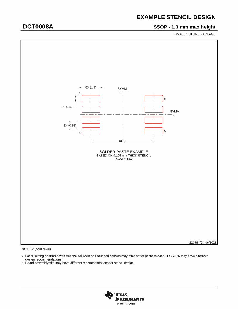
EXAMPLE STENCIL DESIGN
(3.8)
6X (0.65)
8X (0.4)
8X (1.1)
4220784/C 06/2021
SSOP - 1.3 mm max heightDCT0008ASMALL OUTLINE PACKAGE
NOTES: (continued) 7. Laser cutting apertures with trapezoidal walls and rounded corners may offer better paste release. IPC-7525 may have alternate design recommendations. 8. Board assembly site may have different recommendations for stencil design.
SYMM
SYMM
1
4 5
8
SOLDER PASTE EXAMPLEBASED ON 0.125 mm THICK STENCIL
SCALE:15X
www.ti.com
PACKAGE OUTLINE
C0.5 MAX
0.190.15
1.5TYP
0.5 TYP
8X 0.250.21
0.5TYP
B E A
D
4223082/A 07/2016
DSBGA - 0.5 mm max heightYZP0008DIE SIZE BALL GRID ARRAY
NOTES: 1. All linear dimensions are in millimeters. Any dimensions in parenthesis are for reference only. Dimensioning and tolerancing per ASME Y14.5M.2. This drawing is subject to change without notice.
BALL A1CORNER
SEATING PLANE
BALL TYP0.05 C
B
1 2
0.015 C A B
SYMM
SYMM
C
A
D
SCALE 8.000
D: Max =
E: Max =
1.919 mm, Min =
0.918 mm, Min =
1.858 mm
0.857 mm
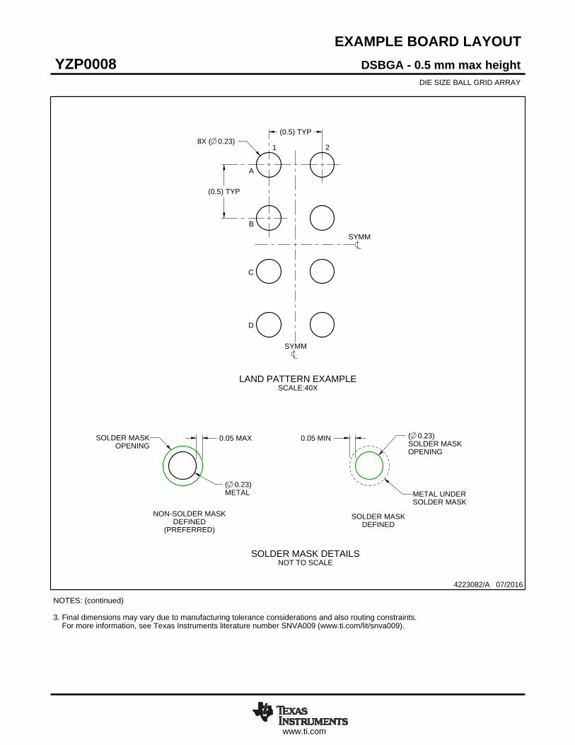
www.ti.com
EXAMPLE BOARD LAYOUT
8X ( 0.23)(0.5) TYP
(0.5) TYP
( 0.23)METAL
0.05 MAX ( 0.23)SOLDER MASKOPENING
0.05 MIN
4223082/A 07/2016
DSBGA - 0.5 mm max heightYZP0008DIE SIZE BALL GRID ARRAY
NOTES: (continued) 3. Final dimensions may vary due to manufacturing tolerance considerations and also routing constraints. For more information, see Texas Instruments literature number SNVA009 (www.ti.com/lit/snva009).
SYMM
SYMM
LAND PATTERN EXAMPLESCALE:40X
1 2
A
B
C
D
NON-SOLDER MASKDEFINED
(PREFERRED)
SOLDER MASK DETAILSNOT TO SCALE
SOLDER MASKOPENING
SOLDER MASKDEFINED
METAL UNDERSOLDER MASK
www.ti.com
EXAMPLE STENCIL DESIGN
(0.5)TYP
(0.5) TYP
8X ( 0.25) (R0.05) TYP
METALTYP
4223082/A 07/2016
DSBGA - 0.5 mm max heightYZP0008DIE SIZE BALL GRID ARRAY
NOTES: (continued) 4. Laser cutting apertures with trapezoidal walls and rounded corners may offer better paste release.
SYMM
SYMM
SOLDER PASTE EXAMPLEBASED ON 0.1 mm THICK STENCIL
SCALE:40X
1 2
A
B
C
D
IMPORTANT NOTICE AND DISCLAIMERTI PROVIDES TECHNICAL AND RELIABILITY DATA (INCLUDING DATA SHEETS), DESIGN RESOURCES (INCLUDING REFERENCE DESIGNS), APPLICATION OR OTHER DESIGN ADVICE, WEB TOOLS, SAFETY INFORMATION, AND OTHER RESOURCES “AS IS” AND WITH ALL FAULTS, AND DISCLAIMS ALL WARRANTIES, EXPRESS AND IMPLIED, INCLUDING WITHOUT LIMITATION ANY IMPLIED WARRANTIES OF MERCHANTABILITY, FITNESS FOR A PARTICULAR PURPOSE OR NON-INFRINGEMENT OF THIRD PARTY INTELLECTUAL PROPERTY RIGHTS.These resources are intended for skilled developers designing with TI products. You are solely responsible for (1) selecting the appropriate TI products for your application, (2) designing, validating and testing your application, and (3) ensuring your application meets applicable standards, and any other safety, security, regulatory or other requirements.These resources are subject to change without notice. TI grants you permission to use these resources only for development of an application that uses the TI products described in the resource. Other reproduction and display of these resources is prohibited. No license is granted to any other TI intellectual property right or to any third party intellectual property right. TI disclaims responsibility for, and you will fully indemnify TI and its representatives against, any claims, damages, costs, losses, and liabilities arising out of your use of these resources.TI’s products are provided subject to TI’s Terms of Sale or other applicable terms available either on ti.com or provided in conjunction with such TI products. TI’s provision of these resources does not expand or otherwise alter TI’s applicable warranties or warranty disclaimers for TI products.TI objects to and rejects any additional or different terms you may have proposed. IMPORTANT NOTICE
Mailing Address: Texas Instruments, Post Office Box 655303, Dallas, Texas 75265Copyright © 2022, Texas Instruments Incorporated