TPS763 Low-Power 150-mA Low-Dropout Linear … has enabled the usual pnp pass transistor ... 9...
29
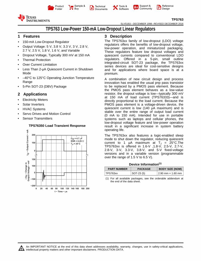
150 -100 100 200 0 100 0 t - Time - μs C O = 4.7 μF ESR = 0.25 Ω T J = 25°C 0 60 40 20 80 100 140 120 160 180 200 I - Output Current - mA O V O - Change in Δ Output Voltage - mV -200 Product Folder Sample & Buy Technical Documents Tools & Software Support & Community Reference Design An IMPORTANT NOTICE at the end of this data sheet addresses availability, warranty, changes, use in safety-critical applications, intellectual property matters and other important disclaimers. PRODUCTION DATA. TPS763 SLVS181I – DECEMBER 1998 – REVISED DECEMBER 2016 TPS763 Low-Power 150-mA Low-Dropout Linear Regulators 1 1 Features 1• 150-mA Low-Dropout Regulator • Output Voltage: 5 V, 3.8 V, 3.3 V, 3 V, 2.8 V, 2.7 V, 2.5 V, 1.8 V, 1.6 V, and Variable • Dropout Voltage, Typically 300 mV at 150 mA • Thermal Protection • Over Current Limitation • Less Than 2-μA Quiescent Current in Shutdown Mode • –40°C to 125°C Operating Junction Temperature Range • 5-Pin SOT-23 (DBV) Package 2 Applications • Electricity Meters • Solar Inverters • HVAC Systems • Servo Drives and Motion Control • Sensor Transmitters TPS76350 Load Transient Response 3 Description The TPS763xx family of low-dropout (LDO) voltage regulators offers the benefits of low-dropout voltage, low-power operation, and miniaturized packaging. These regulators feature low dropout voltages and quiescent currents compared to conventional LDO regulators. Offered in a 5-pin, small outline integrated-circuit SOT-23 package, the TPS763xx series devices are ideal for cost-sensitive designs and for applications where board space is at a premium. A combination of new circuit design and process innovation has enabled the usual pnp pass transistor to be replaced by a PMOS pass element. Because the PMOS pass element behaves as a low-value resistor, the dropout voltage is low—typically 300 mV at 150 mA of load current (TPS76333)—and is directly proportional to the load current. Because the PMOS pass element is a voltage-driven device, the quiescent current is low (140 μA maximum) and is stable over the entire range of output load current (0 mA to 150 mA). Intended for use in portable systems such as laptops and cellular phones, the low-dropout voltage feature and low-power operation result in a significant increase in system battery operating life. The TPS763xx also features a logic-enabled sleep mode to shut down the regulator, reducing quiescent current to 1 μA maximum at T J = 25°C.The TPS763xx is offered in 1.6-V ,1.8-V, 2.5-V, 2.7-V, 2.8-V, 3-V, 3.3-V, 3.8-V, and 5-V fixed-voltage versions and in a variable version (programmable over the range of 1.5 V to 6.5 V). Device Information (1) PART NUMBER PACKAGE BODY SIZE (NOM) TPS763xx SOT-23 (5) 2.90 mm × 1.60 mm (1) For all available packages, see the orderable addendum at the end of the data sheet.
Transcript of TPS763 Low-Power 150-mA Low-Dropout Linear … has enabled the usual pnp pass transistor ... 9...
150
−100
100
200
0
100
0
t − Time − µs
CO = 4.7 µF
ESR = 0.25 Ω
TJ = 25°C
0 604020 80 100 140120 160 180 200
I−
Ou
tpu
t C
urr
en
t−
mA
OV
O−
Ch
an
ge
in
∆
Ou
tpu
tV
olt
ag
e−
mV
−200
Product
Folder
Sample &Buy
Technical
Documents
Tools &
Software
Support &Community
ReferenceDesign
An IMPORTANT NOTICE at the end of this data sheet addresses availability, warranty, changes, use in safety-critical applications,intellectual property matters and other important disclaimers. PRODUCTION DATA.
TPS763SLVS181I –DECEMBER 1998–REVISED DECEMBER 2016
TPS763 Low-Power 150-mA Low-Dropout Linear Regulators
1
1 Features1• 150-mA Low-Dropout Regulator• Output Voltage: 5 V, 3.8 V, 3.3 V, 3 V, 2.8 V,
2.7 V, 2.5 V, 1.8 V, 1.6 V, and Variable• Dropout Voltage, Typically 300 mV at 150 mA• Thermal Protection• Over Current Limitation• Less Than 2-µA Quiescent Current in Shutdown
Mode• –40°C to 125°C Operating Junction Temperature
Range• 5-Pin SOT-23 (DBV) Package
2 Applications• Electricity Meters• Solar Inverters• HVAC Systems• Servo Drives and Motion Control• Sensor Transmitters
TPS76350 Load Transient Response
3 DescriptionThe TPS763xx family of low-dropout (LDO) voltageregulators offers the benefits of low-dropout voltage,low-power operation, and miniaturized packaging.These regulators feature low dropout voltages andquiescent currents compared to conventional LDOregulators. Offered in a 5-pin, small outlineintegrated-circuit SOT-23 package, the TPS763xxseries devices are ideal for cost-sensitive designsand for applications where board space is at apremium.
A combination of new circuit design and processinnovation has enabled the usual pnp pass transistorto be replaced by a PMOS pass element. Becausethe PMOS pass element behaves as a low-valueresistor, the dropout voltage is low—typically 300 mVat 150 mA of load current (TPS76333)—and isdirectly proportional to the load current. Because thePMOS pass element is a voltage-driven device, thequiescent current is low (140 µA maximum) and isstable over the entire range of output load current(0 mA to 150 mA). Intended for use in portablesystems such as laptops and cellular phones, thelow-dropout voltage feature and low-power operationresult in a significant increase in system batteryoperating life.
The TPS763xx also features a logic-enabled sleepmode to shut down the regulator, reducing quiescentcurrent to 1 µA maximum at TJ = 25°C.TheTPS763xx is offered in 1.6-V ,1.8-V, 2.5-V, 2.7-V,2.8-V, 3-V, 3.3-V, 3.8-V, and 5-V fixed-voltageversions and in a variable version (programmableover the range of 1.5 V to 6.5 V).
Device Information(1)
PART NUMBER PACKAGE BODY SIZE (NOM)TPS763xx SOT-23 (5) 2.90 mm × 1.60 mm
(1) For all available packages, see the orderable addendum atthe end of the data sheet.
2
TPS763SLVS181I –DECEMBER 1998–REVISED DECEMBER 2016 www.ti.com
Product Folder Links: TPS763
Submit Documentation Feedback Copyright © 1998–2016, Texas Instruments Incorporated
Table of Contents1 Features .................................................................. 12 Applications ........................................................... 13 Description ............................................................. 14 Revision History..................................................... 25 Pin Configuration and Functions ......................... 36 Specifications......................................................... 37 Absolute Maximum Ratings.................................. 38 ESD Ratings ........................................................... 39 Recommended Operating Conditions ................. 310 Thermal Information.............................................. 411 Electrical Characteristics ..................................... 4
11.1 Typical Characteristics ............................................ 712 Detailed Description ........................................... 11
12.1 Overview ............................................................... 1112.2 Functional Block Diagram ..................................... 1112.3 Feature Description............................................... 11
12.4 Device Functional Modes...................................... 1213 Application and Implementation........................ 13
13.1 Application Information.......................................... 1313.2 Typical Application ................................................ 13
14 Power Supply Recommendations ..................... 1614.1 Power Dissipation and Junction Temperature ...... 16
15 Layout................................................................... 1615.1 Layout Guidelines ................................................. 1615.2 Layout Example .................................................... 16
16 Device and Documentation Support ................. 1716.1 Receiving Notification of Documentation Updates 1716.2 Community Resources.......................................... 1716.3 Trademarks ........................................................... 1716.4 Electrostatic Discharge Caution............................ 1716.5 Glossary ................................................................ 17
17 Mechanical, Packaging, and OrderableInformation ........................................................... 17
4 Revision HistoryNOTE: Page numbers for previous revisions may differ from page numbers in the current version.
Changes from Revision H (January 2004) to Revision I Page
• Added ESD Ratings table, Feature Description section, Device Functional Modes, Application and Implementationsection, Power Supply Recommendations section, Layout section, Device and Documentation Support section, andMechanical, Packaging, and Orderable Information section .................................................................................................. 1
• Deleted Legacy Applications and Non-Ceramic Capacitor Stability from Applications ......................................................... 1• Added Electricity Meters, Solar Inverters, HVAC Systems, Servo Drives and Motion Control, and Sensor
Transmitters to Applications ................................................................................................................................................... 1• Deleted Dissipation Ratings table........................................................................................................................................... 3• Added Thermal Information table ........................................................................................................................................... 4
3
2
4
51IN
GND
EN
OUT
NC/FB
3
TPS763www.ti.com SLVS181I –DECEMBER 1998–REVISED DECEMBER 2016
Product Folder Links: TPS763
Submit Documentation FeedbackCopyright © 1998–2016, Texas Instruments Incorporated
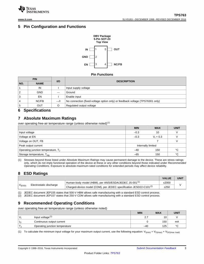
5 Pin Configuration and Functions
DBV Package5-Pin SOT-23
Top View
Pin FunctionsPIN
I/O DESCRIPTIONNO. NAME1 IN I Input supply voltage2 GND — Ground3 EN I Enable input4 NC/FB —/I No connection (fixed-voltage option only) or feedback voltage (TPS76301 only)5 OUT O Regulated output voltage
(1) Stresses beyond those listed under Absolute Maximum Ratings may cause permanent damage to the device. These are stress ratingsonly, which do not imply functional operation of the device at these or any other conditions beyond those indicated under RecommendedOperating Conditions. Exposure to absolute-maximum-rated conditions for extended periods may affect device reliability.
6 Specifications
7 Absolute Maximum Ratingsover operating free-air temperature range (unless otherwise noted) (1)
MIN MAX UNITInput voltage –0.3 10 VVoltage at EN –0.3 VI + 0.3 VVoltage on OUT, FB 7 VPeak output current Internally limitedOperating junction temperature, TJ –40 150 °CStorage temperature, Tstg –65 150 °C
(1) JEDEC document JEP155 states that 500-V HBM allows safe manufacturing with a standard ESD control process.(2) JEDEC document JEP157 states that 250-V CDM allows safe manufacturing with a standard ESD control process.
8 ESD RatingsVALUE UNIT
V(ESD) Electrostatic dischargeHuman-body model (HBM), per ANSI/ESDA/JEDEC JS-001 (1) ±2000
VCharged-device model (CDM), per JEDEC specification JESD22-C101 (2) ±250
(1) To calculate the minimum input voltage for your maximum output current, use the following equation: VI(min) = VO(max) + VDO(max load)
9 Recommended Operating Conditionsover operating free-air temperature range (unless otherwise noted)
MIN MAX UNITVI Input voltage (1) 2.7 10 VIO Continuous output current 0 150 mATJ Operating junction temperature –40 125 °C
4
TPS763SLVS181I –DECEMBER 1998–REVISED DECEMBER 2016 www.ti.com
Product Folder Links: TPS763
Submit Documentation Feedback Copyright © 1998–2016, Texas Instruments Incorporated
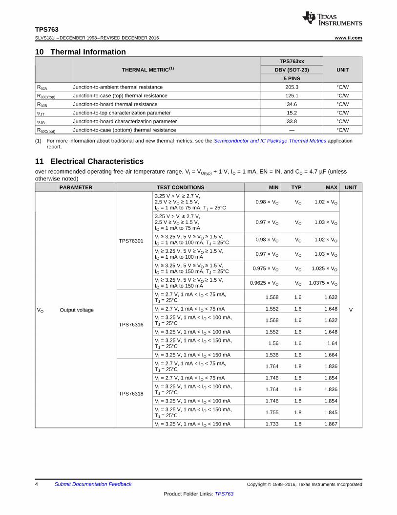
(1) For more information about traditional and new thermal metrics, see the Semiconductor and IC Package Thermal Metrics applicationreport.
10 Thermal Information
THERMAL METRIC (1)TPS763xx
UNITDBV (SOT-23)5 PINS
RθJA Junction-to-ambient thermal resistance 205.3 °C/WRθJC(top) Junction-to-case (top) thermal resistance 125.1 °C/WRθJB Junction-to-board thermal resistance 34.6 °C/WψJT Junction-to-top characterization parameter 15.2 °C/WψJB Junction-to-board characterization parameter 33.8 °C/WRθJC(bot) Junction-to-case (bottom) thermal resistance — °C/W
11 Electrical Characteristicsover recommended operating free-air temperature range, VI = VO(typ) + 1 V, IO = 1 mA, EN = IN, and CO = 4.7 µF (unlessotherwise noted)
PARAMETER TEST CONDITIONS MIN TYP MAX UNIT
VO Output voltage
TPS76301
3.25 V > VI ≥ 2.7 V,2.5 V ≥ VO ≥ 1.5 V,IO = 1 mA to 75 mA, TJ = 25°C
0.98 × VO VO 1.02 × VO
V
3.25 V > VI ≥ 2.7 V,2.5 V ≥ VO ≥ 1.5 V,IO = 1 mA to 75 mA
0.97 × VO VO 1.03 × VO
VI ≥ 3.25 V, 5 V ≥ VO ≥ 1.5 V,IO = 1 mA to 100 mA, TJ = 25°C 0.98 × VO VO 1.02 × VO
VI ≥ 3.25 V, 5 V ≥ VO ≥ 1.5 V,IO = 1 mA to 100 mA 0.97 × VO VO 1.03 × VO
VI ≥ 3.25 V, 5 V ≥ VO ≥ 1.5 V,IO = 1 mA to 150 mA, TJ = 25°C 0.975 × VO VO 1.025 × VO
VI ≥ 3.25 V, 5 V ≥ VO ≥ 1.5 V,IO = 1 mA to 150 mA 0.9625 × VO VO 1.0375 × VO
TPS76316
VI = 2.7 V, 1 mA < IO < 75 mA,TJ = 25°C 1.568 1.6 1.632
VI = 2.7 V, 1 mA < IO < 75 mA 1.552 1.6 1.648VI = 3.25 V, 1 mA < IO < 100 mA,TJ = 25°C 1.568 1.6 1.632
VI = 3.25 V, 1 mA < IO < 100 mA 1.552 1.6 1.648VI = 3.25 V, 1 mA < IO < 150 mA,TJ = 25°C 1.56 1.6 1.64
VI = 3.25 V, 1 mA < IO < 150 mA 1.536 1.6 1.664
TPS76318
VI = 2.7 V, 1 mA < IO < 75 mA,TJ = 25°C 1.764 1.8 1.836
VI = 2.7 V, 1 mA < IO < 75 mA 1.746 1.8 1.854VI = 3.25 V, 1 mA < IO < 100 mA,TJ = 25°C 1.764 1.8 1.836
VI = 3.25 V, 1 mA < IO < 100 mA 1.746 1.8 1.854VI = 3.25 V, 1 mA < IO < 150 mA,TJ = 25°C 1.755 1.8 1.845
VI = 3.25 V, 1 mA < IO < 150 mA 1.733 1.8 1.867
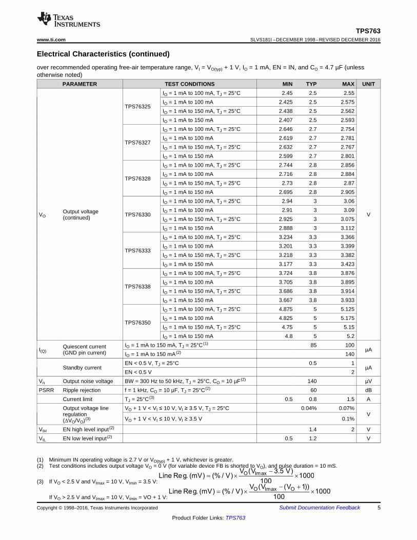
O Imax OV (V (V 1))Line Reg. (mV) (% / V) 1000
100
- +
= ´ ´
O ImaxV (V 3.5 V)Line Reg. (mV) (% / V) 1000
100
-
= ´ ´
5
TPS763www.ti.com SLVS181I –DECEMBER 1998–REVISED DECEMBER 2016
Product Folder Links: TPS763
Submit Documentation FeedbackCopyright © 1998–2016, Texas Instruments Incorporated
Electrical Characteristics (continued)over recommended operating free-air temperature range, VI = VO(typ) + 1 V, IO = 1 mA, EN = IN, and CO = 4.7 µF (unlessotherwise noted)
PARAMETER TEST CONDITIONS MIN TYP MAX UNIT
(1) Minimum IN operating voltage is 2.7 V or VO(typ) + 1 V, whichever is greater.(2) Test conditions includes output voltage VO = 0 V (for variable device FB is shorted to VO), and pulse duration = 10 mS.
(3) If VO < 2.5 V and VImax = 10 V, VImin = 3.5 V:
If VO > 2.5 V and VImax = 10 V, VImin = VO + 1 V:
VOOutput voltage(continued)
TPS76325
IO = 1 mA to 100 mA, TJ = 25°C 2.45 2.5 2.55
V
IO = 1 mA to 100 mA 2.425 2.5 2.575IO = 1 mA to 150 mA, TJ = 25°C 2.438 2.5 2.562IO = 1 mA to 150 mA 2.407 2.5 2.593
TPS76327
IO = 1 mA to 100 mA, TJ = 25°C 2.646 2.7 2.754IO = 1 mA to 100 mA 2.619 2.7 2.781IO = 1 mA to 150 mA, TJ = 25°C 2.632 2.7 2.767IO = 1 mA to 150 mA 2.599 2.7 2.801
TPS76328
IO = 1 mA to 100 mA, TJ = 25°C 2.744 2.8 2.856IO = 1 mA to 100 mA 2.716 2.8 2.884IO = 1 mA to 150 mA, TJ = 25°C 2.73 2.8 2.87IO = 1 mA to 150 mA 2.695 2.8 2.905
TPS76330
IO = 1 mA to 100 mA, TJ = 25°C 2.94 3 3.06IO = 1 mA to 100 mA 2.91 3 3.09IO = 1 mA to 150 mA, TJ = 25°C 2.925 3 3.075IO = 1 mA to 150 mA 2.888 3 3.112
TPS76333
IO = 1 mA to 100 mA, TJ = 25°C 3.234 3.3 3.366IO = 1 mA to 100 mA 3.201 3.3 3.399IO = 1 mA to 150 mA, TJ = 25°C 3.218 3.3 3.382IO = 1 mA to 150 mA 3.177 3.3 3.423
TPS76338
IO = 1 mA to 100 mA, TJ = 25°C 3.724 3.8 3.876IO = 1 mA to 100 mA 3.705 3.8 3.895IO = 1 mA to 150 mA, TJ = 25°C 3.686 3.8 3.914IO = 1 mA to 150 mA 3.667 3.8 3.933
TPS76350
IO = 1 mA to 100 mA, TJ = 25°C 4.875 5 5.125IO = 1 mA to 100 mA 4.825 5 5.175IO = 1 mA to 150 mA, TJ = 25°C 4.75 5 5.15IO = 1 mA to 150 mA 4.8 5 5.2
I(Q)Quiescent current(GND pin current)
IO = 1 mA to 150 mA, TJ = 25°C (1) 85 100µA
IO = 1 mA to 150 mA (2) 140
Standby currentEN < 0.5 V, TJ = 25°C 0.5 1
µAEN < 0.5 V 2
Vn Output noise voltage BW = 300 Hz to 50 kHz, TJ = 25°C, CO = 10 µF (2) 140 µVPSRR Ripple rejection f = 1 kHz, CO = 10 µF, TJ = 25°C (2) 60 dB
Current limit TJ = 25°C (3) 0.5 0.8 1.5 AOutput voltage lineregulation(ΔVO/VO)(3)
VO + 1 V < VI ≤ 10 V, VI ≥ 3.5 V, TJ = 25°C 0.04% 0.07%V
VO + 1 V < VI ≤ 10 V, VI ≥ 3.5 V 0.1%
VIH EN high level input (2) 1.4 2 VVIL EN low level input (2) 0.5 1.2 V
6
TPS763SLVS181I –DECEMBER 1998–REVISED DECEMBER 2016 www.ti.com
Product Folder Links: TPS763
Submit Documentation Feedback Copyright © 1998–2016, Texas Instruments Incorporated
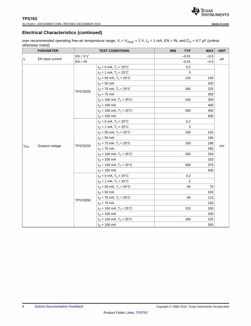
Electrical Characteristics (continued)over recommended operating free-air temperature range, VI = VO(typ) + 1 V, IO = 1 mA, EN = IN, and CO = 4.7 µF (unlessotherwise noted)
PARAMETER TEST CONDITIONS MIN TYP MAX UNIT
II EN input currentEN = 0 V –0.01 –0.5
µAEN = IN –0.01 –0.5
VDO Dropout voltage
TPS76325
IO = 0 mA, TJ = 25°C 0.2
mV
IO = 1 mA, TJ = 25°C 3IO = 50 mA, TJ = 25°C 120 150IO = 50 mA 200IO = 75 mA, TJ = 25°C 180 225IO = 75 mA 300IO = 100 mA, TJ = 25°C 240 300IO = 100 mA 400IO = 150 mA, TJ = 25°C 360 450IO = 150 mA 600
TPS76333
IO = 0 mA, TJ = 25°C 0.2IO = 1 mA, TJ = 25°C 3IO = 50 mA, TJ = 25°C 100 125IO = 50 mA 166IO = 75 mA, TJ = 25°C 150 188IO = 75 mA 250IO = 100 mA, TJ = 25°C 200 250IO = 100 mA 333IO = 150 mA, TJ = 25°C 300 375IO = 150 mA 500
TPS76350
IO = 0 mA, TJ = 25°C 0.2IO = 1 mA, TJ = 25°C 2IO = 50 mA, TJ = 25°C 60 75IO = 50 mA 100IO = 75 mA, TJ = 25°C 90 113IO = 75 mA 150IO = 100 mA, TJ = 25°C 120 150IO = 100 mA 200IO = 150 mA, TJ = 25°C 180 225IO = 150 mA 300
TJ − Junction Temperature − °C
1.74−35 5
1.8
1.78
−15 25 125
1.82
−55 45 65 85 105
IO = 150 mA
IO = 1 mA
−O
utp
ut
Vo
ltag
e−
VV
O
1.75
1.79
1.76
1.81
1.77
VI = 3.5 V
CI = CO = 4.7 µF
TJ − Junction Temperature − °C
5.02
4.98
4.94
4.9−35 5
5.04
5
4.96
4.92
−15 25 125
5.1
−55 45 65
5.06
5.08
85 105
IO = 150 mA
IO = 1 mA
−O
utp
ut
Vo
ltag
e−
VV
O
VI = 6 V
CI = CO = 4.7 µF
IO − Output Current − mA
5
4.97
4.9530 90
4.99
4.98
4.96
60 120 180
5.01
0 150
−O
utp
ut
Vo
ltag
e−
VV
O
VI = 6 V
CI = CO = 4.7 µF
TJ = 25°C
TJ − Junction Temperature − °C
2.49
2.47−35 5
2.5
2.48
−15 25 125
2.53
−55 45 65
2.51
2.52
85 105
IO = 150 mA
IO = 1 mA
−O
utp
ut
Vo
ltag
e−
VV
O
VI = 3.5 V
CI = CO = 4.7 µF
IO − Output Current − mA
2.5
2.485
2.47530 90
2.495
2.49
2.48
60 120 180
2.505
0 150
VI = 3.5 V
CI = CO = 4.7 µF
TJ = 25°C
−O
utp
ut
Vo
ltag
e−
VV
O
IO − Output Current − mA
1.795
1.780
1.77030 90
1.790
1.785
1.775
60 120 180
1.805
0 150
−O
utp
ut
Vo
ltag
e−
VV
O
1.800
VI = 3.5 V
CI = CO = 4.7 µF
TJ = 25°C
7
TPS763www.ti.com SLVS181I –DECEMBER 1998–REVISED DECEMBER 2016
Product Folder Links: TPS763
Submit Documentation FeedbackCopyright © 1998–2016, Texas Instruments Incorporated
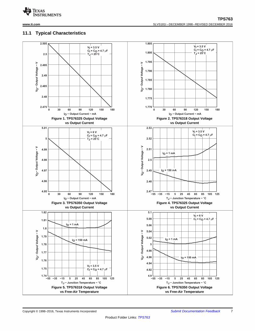
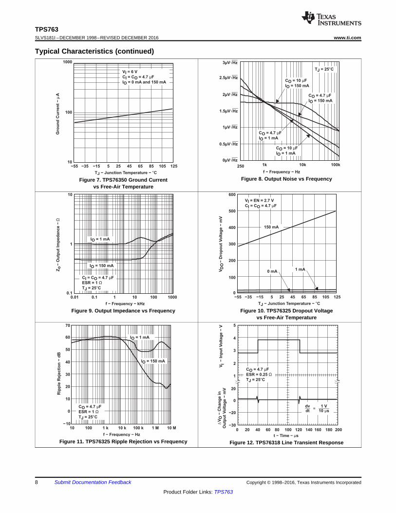
11.1 Typical Characteristics
Figure 1. TPS76325 Output Voltagevs Output Current
Figure 2. TPS76318 Output Voltagevs Output Current
Figure 3. TPS76350 Output Voltagevs Output Current
Figure 4. TPS76325 Output Voltagevs Output Current
Figure 5. TPS76318 Output Voltagevs Free-Air Temperature
Figure 6. TPS76350 Output Voltagevs Free-Air Temperature
VO
−C
han
ge in
4
2
3
1
0
−20
20
VI
t − Time − µs
0 604020 80 100 140120 160 180 200
−In
pu
t V
olt
ag
e−
V∆
Ou
tpu
tV
olt
ag
e−
mV
−30
CO = 4.7 µF
ESR = 0.25 Ω
TJ = 25°C
dvdt
1 V10 µs
5
=
10 M1 M100 k10 k1 k100
Rip
ple
Reje
cti
on
−d
B
f − Frequency − Hz
70
60
50
40
30
20
10
0
−1010
CO = 4.7 µF
ESR = 1 Ω
TJ = 25°C
IO = 150 mA
IO = 1 mA
0.10.1 1 1000
10
0.01 10
1
f − Frequency − kHz
100
−O
utp
ut
Imp
ed
an
ce
−Z
oΩ
CI = CO = 4.7 µF
ESR = 1 Ω
TJ = 25°C
IO = 150 mA
IO = 1 mA
TJ − Junction Temperature − °C
200
0−35 5
300
100
−15 25 125
600
−55 45 65
400
500
VI = EN = 2.7 V
CI = CO = 4.7 µF
85 105
1 mA
−D
rop
ou
tV
olt
ag
e−
mV
VD
O
150 mA
0 mA
TJ − Junction Temperature − °C
100
10−35 5−15 25 125−55 45 65
1000
85 105
Gro
un
d C
urr
en
t−
Aµ
VI = 6 V
CI = CO = 4.7 µF
IO = 0 mA and 150 mA
f − Frequency − Hz
1k 10k 100k250
CO = 4.7 µF
IO = 1 mA
CO = 4.7 µF
IO = 150 mA
CO = 10 µF
IO = 150 mA
CO = 10 µF
IO = 1 mA
TJ = 25°C
3µV HzÖ
2.5µV HzÖ
2µV HzÖ
1µV HzÖ
0µV HzÖ
1.5µV HzÖ
0.5µV HzÖ
8
TPS763SLVS181I –DECEMBER 1998–REVISED DECEMBER 2016 www.ti.com
Product Folder Links: TPS763
Submit Documentation Feedback Copyright © 1998–2016, Texas Instruments Incorporated
Typical Characteristics (continued)
Figure 7. TPS76350 Ground Currentvs Free-Air Temperature
Figure 8. Output Noise vs Frequency
Figure 9. Output Impedance vs Frequency Figure 10. TPS76325 Dropout Voltagevs Free-Air Temperature
Figure 11. TPS76325 Ripple Rejection vs Frequency Figure 12. TPS76318 Line Transient Response
0.1
0.010 50 100 150 200 250
10
100
IO − Output Current − mA
1
Region of Instability
CS
R−
Co
mp
en
sati
on
Seri
es R
esis
tan
ce
−Ω
Region of Instability
CO = 10 µF
0.1
0.010 0.1 0.2 0.3 0.4 0.5
10
100
Added Ceramic Capacitance − µF
0.6 0.7 0.8 0.9 1
1
Region of Instability
Region of Instability
CS
R−
Co
mp
en
sati
on
Seri
es R
esis
tan
ce
−Ω
I = 150 mACO = 4.7 µFTJ = 25°C
150
−100
100
200
0
100
0
t − Time − µs
CO = 4.7 µF
ESR = 0.25 Ω
TJ = 25°C
0 604020 80 100 140120 160 180 200
I−
Ou
tpu
t C
urr
en
t−
mA
OV
O−
Ch
an
ge
in
∆
Ou
tpu
tV
olt
ag
e−
mV
−200
0.1
0.010 50 100 150 200 250
10
100
IO − Output Current − mA
CS
R−
Co
mp
en
sati
on
Seri
es
Resis
tan
ce
−Ω
1
Region of Instability
CO = 4.7 µFTJ = 25°C
Region of Instability
5
−50
0
−100
7
6
8
t − Time − µs
0 15010050 200 250 350300 400 450 500
VO
−C
han
ge in
VI
−In
pu
t V
olt
ag
e−
V∆
Ou
tpu
tV
olt
ag
e−
mV
50
dvdt
1 V10 µs
CO = 4.7 µF
ESR = 0.25 Ω
TJ = 25°C
=
50
−50
0
−100
100
0
200
t − Time − µs
CO = 4.7 µF
ESR = 0.25 Ω
TJ = 25°C
0 604020 80 100 140120 160 180 200
I−
Ou
tpu
t C
urr
en
t−
mA
OV
O−
Ch
an
ge
in
∆
Ou
tpu
tV
olt
ag
e−
mV
−150
9
TPS763www.ti.com SLVS181I –DECEMBER 1998–REVISED DECEMBER 2016
Product Folder Links: TPS763
Submit Documentation FeedbackCopyright © 1998–2016, Texas Instruments Incorporated
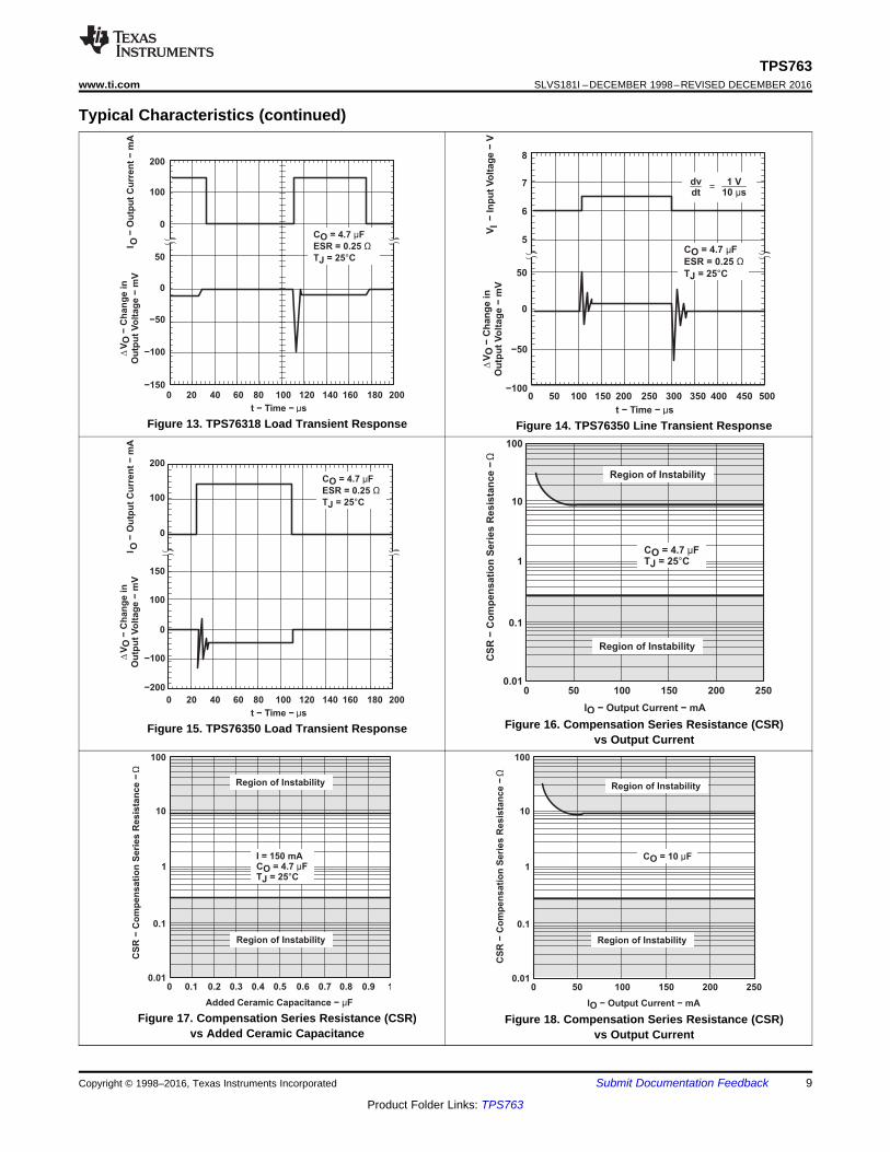
Typical Characteristics (continued)
Figure 13. TPS76318 Load Transient Response Figure 14. TPS76350 Line Transient Response
Figure 15. TPS76350 Load Transient Response Figure 16. Compensation Series Resistance (CSR)vs Output Current
Figure 17. Compensation Series Resistance (CSR)vs Added Ceramic Capacitance
Figure 18. Compensation Series Resistance (CSR)vs Output Current
0.1
0.010 0.1 0.2 0.3 0.4 0.5
10
100
Added Ceramic Capacitance − µF
1
0.6 0.7 0.8 0.9 1
CS
R−
Co
mp
en
sati
on
Seri
es
Resis
tan
ce
−Ω
CO = 10 µF
Region of Instability
Region of Instability
10
TPS763SLVS181I –DECEMBER 1998–REVISED DECEMBER 2016 www.ti.com
Product Folder Links: TPS763
Submit Documentation Feedback Copyright © 1998–2016, Texas Instruments Incorporated
Typical Characteristics (continued)
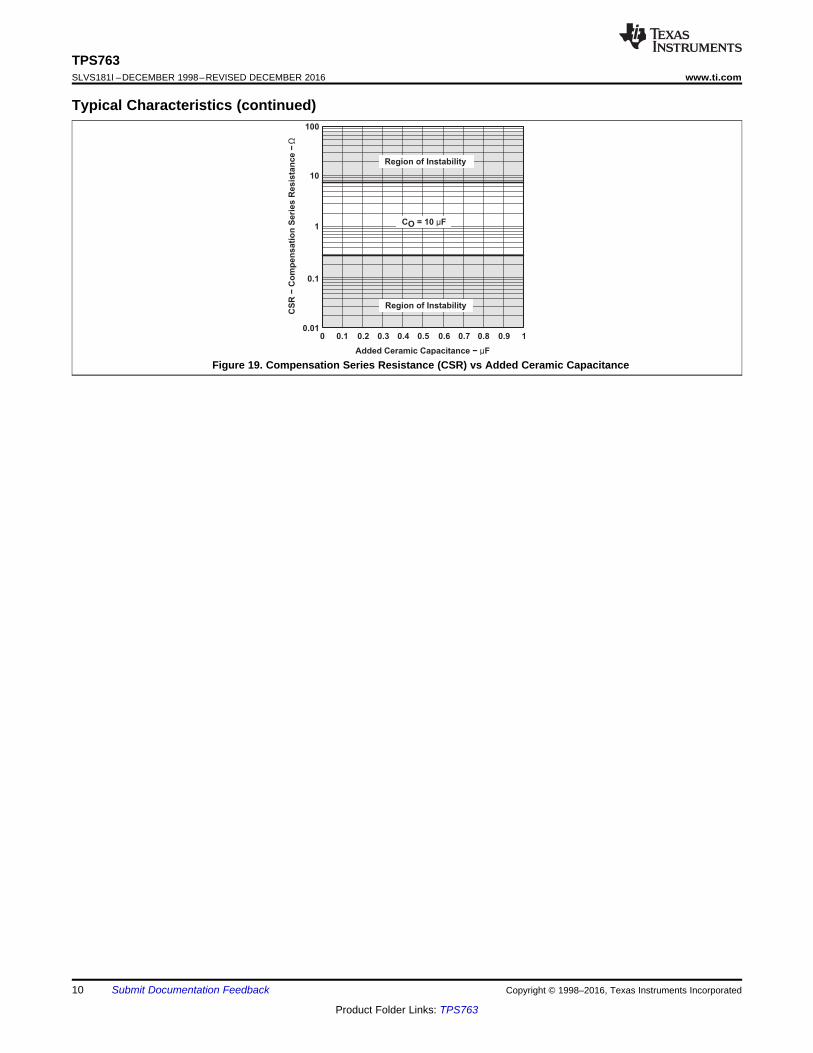
Figure 19. Compensation Series Resistance (CSR) vs Added Ceramic Capacitance
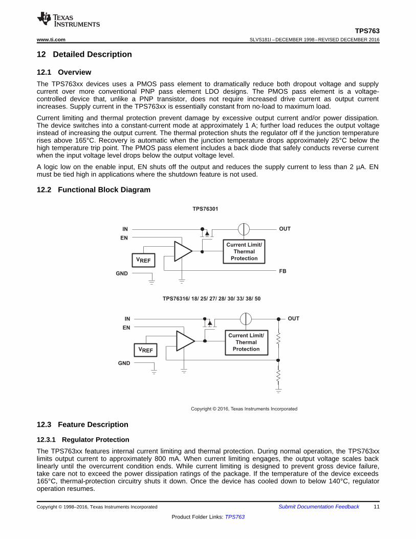
TPS76301
OUTIN
FBGND
EN
VREF
TPS76316/ 18/ 25/ 27/ 28/ 30/ 33/ 38/ 50
OUTIN
GND
EN
VREF
Current Limit/
Thermal
Protection
Current Limit/
Thermal
Protection
Copyright © 2016, Texas Instruments Incorporated
11
TPS763www.ti.com SLVS181I –DECEMBER 1998–REVISED DECEMBER 2016
Product Folder Links: TPS763
Submit Documentation FeedbackCopyright © 1998–2016, Texas Instruments Incorporated
12 Detailed Description
12.1 OverviewThe TPS763xx devices uses a PMOS pass element to dramatically reduce both dropout voltage and supplycurrent over more conventional PNP pass element LDO designs. The PMOS pass element is a voltage-controlled device that, unlike a PNP transistor, does not require increased drive current as output currentincreases. Supply current in the TPS763xx is essentially constant from no-load to maximum load.
Current limiting and thermal protection prevent damage by excessive output current and/or power dissipation.The device switches into a constant-current mode at approximately 1 A; further load reduces the output voltageinstead of increasing the output current. The thermal protection shuts the regulator off if the junction temperaturerises above 165°C. Recovery is automatic when the junction temperature drops approximately 25°C below thehigh temperature trip point. The PMOS pass element includes a back diode that safely conducts reverse currentwhen the input voltage level drops below the output voltage level.
A logic low on the enable input, EN shuts off the output and reduces the supply current to less than 2 µA. ENmust be tied high in applications where the shutdown feature is not used.
12.2 Functional Block Diagram
12.3 Feature Description
12.3.1 Regulator ProtectionThe TPS763xx features internal current limiting and thermal protection. During normal operation, the TPS763xxlimits output current to approximately 800 mA. When current limiting engages, the output voltage scales backlinearly until the overcurrent condition ends. While current limiting is designed to prevent gross device failure,take care not to exceed the power dissipation ratings of the package. If the temperature of the device exceeds165°C, thermal-protection circuitry shuts it down. Once the device has cooled down to below 140°C, regulatoroperation resumes.
12
TPS763SLVS181I –DECEMBER 1998–REVISED DECEMBER 2016 www.ti.com
Product Folder Links: TPS763
Submit Documentation Feedback Copyright © 1998–2016, Texas Instruments Incorporated
Feature Description (continued)
(1) All table conditions must be met.(2) The device is disabled when any condition is met.
12.3.2 EnableThe enable signal (VEN) is an active-high digital control that enables the LDO when the enable voltage is past therising threshold (VEN ≥ VIH(EN)) and disables the LDO when the enable voltage is below the falling threshold(VEN ≤ VIL(EN)). The exact enable threshold is between VIH(EN) and VIL(EN) because EN is a digital control. Inapplications that do not use the enable control, connect EN to VIN.
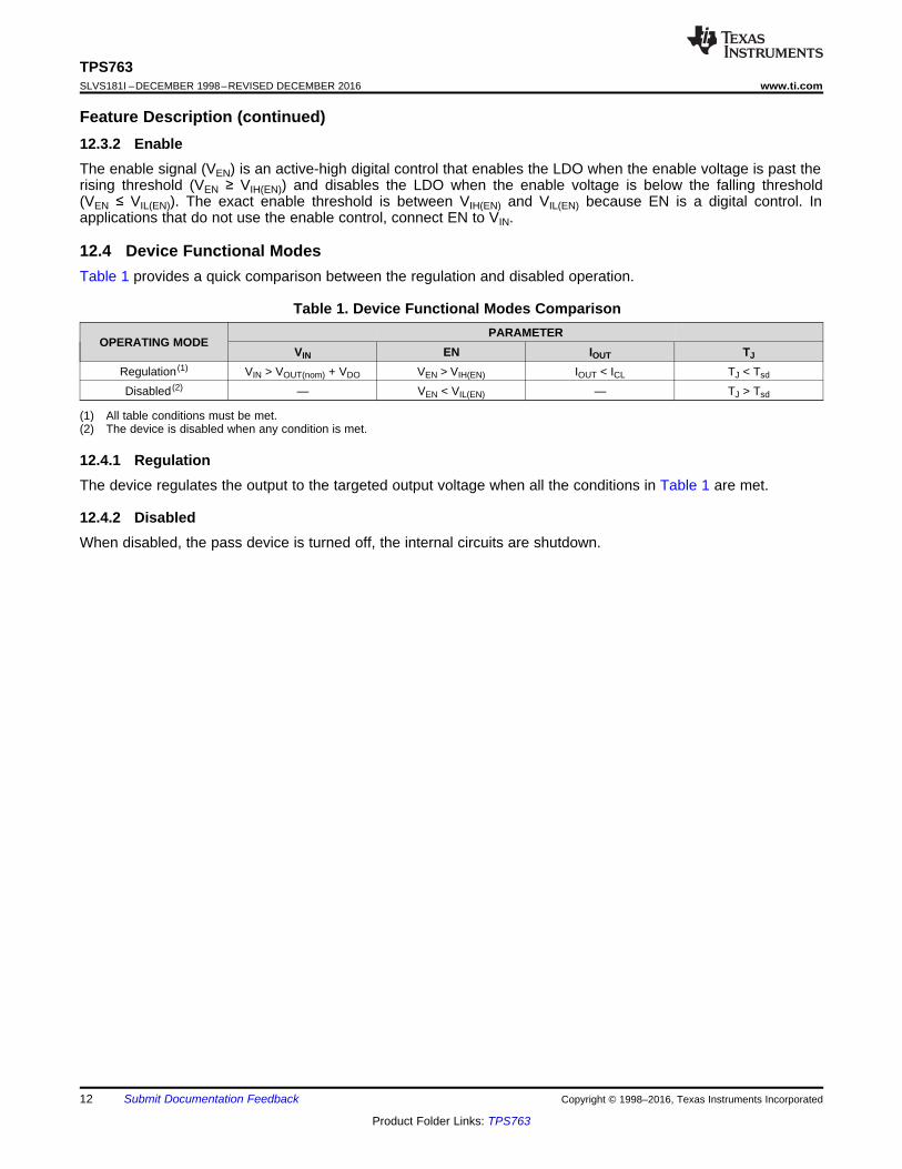
12.4 Device Functional ModesTable 1 provides a quick comparison between the regulation and disabled operation.
Table 1. Device Functional Modes Comparison
OPERATING MODEPARAMETER
VIN EN IOUT TJ
Regulation (1) VIN > VOUT(nom) + VDO VEN > VIH(EN) IOUT < ICL TJ < Tsd
Disabled (2) — VEN < VIL(EN) — TJ > Tsd
12.4.1 RegulationThe device regulates the output to the targeted output voltage when all the conditions in Table 1 are met.
12.4.2 DisabledWhen disabled, the pass device is turned off, the internal circuits are shutdown.
VO
VI
OUT
FB
R2GND
EN
IN
≤0.5 V
≥2 V
TPS76301
1 µF
3
1
4
2
R1
5
CSR = 1 Ω
4.7 µF
+
Copyright © 2016, Texas Instruments Incorporated
13
TPS763www.ti.com SLVS181I –DECEMBER 1998–REVISED DECEMBER 2016
Product Folder Links: TPS763
Submit Documentation FeedbackCopyright © 1998–2016, Texas Instruments Incorporated
13 Application and Implementation
NOTEInformation in the following applications sections is not part of the TI componentspecification, and TI does not warrant its accuracy or completeness. TI’s customers areresponsible for determining suitability of components for their purposes. Customers shouldvalidate and test their design implementation to confirm system functionality.
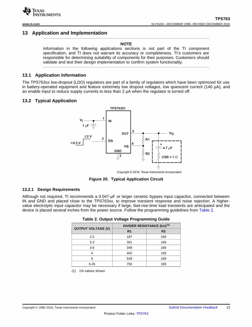
13.1 Application InformationThe TPS763xx low-dropout (LDO) regulators are part of a family of regulators which have been optimized for usein battery-operated equipment and feature extremely low dropout voltages, low quiescent current (140 µA), andan enable input to reduce supply currents to less than 2 µA when the regulator is turned off.
13.2 Typical Application
Figure 20. Typical Application Circuit
13.2.1 Design RequirementsAlthough not required, TI recommends a 0.047-µF or larger ceramic bypass input capacitor, connected betweenIN and GND and placed close to the TPS763xx, to improve transient response and noise rejection. A higher-value electrolytic input capacitor may be necessary if large, fast-rise-time load transients are anticipated and thedevice is placed several inches from the power source. Follow the programming guidelines from Table 2.
(1) 1% values shown
Table 2. Output Voltage Programming Guide
OUTPUT VOLTAGE (V)DIVIDER RESISTANCE (kΩ) (1)
R1 R22.5 187 1693.3 301 1693.6 348 1694 402 1695 549 169
6.45 750 169
VO
VI
OUT
FB
R2GND
EN
IN
≤0.5 V
≥2 V
TPS76301
1 µF
3
1
4
2
R1
5
CSR = 1 Ω
4.7 µF
+
Copyright © 2016, Texas Instruments Incorporated
O
ref
VR1 1 R2
0.995 V
æ ö= - ´ç ÷
´è ø
O ref
R1V 0.995 V 1
R2
æ ö= ´ ´ +ç ÷
è ø
14
TPS763SLVS181I –DECEMBER 1998–REVISED DECEMBER 2016 www.ti.com
Product Folder Links: TPS763
Submit Documentation Feedback Copyright © 1998–2016, Texas Instruments Incorporated
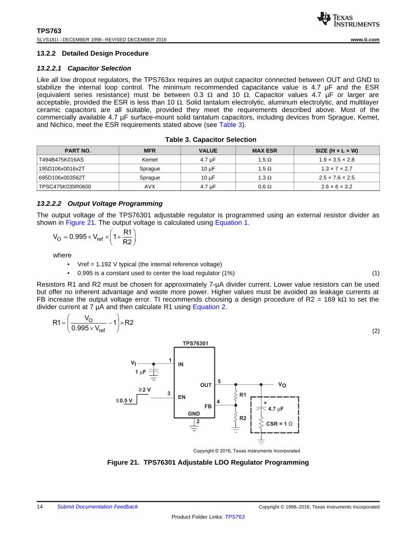
13.2.2 Detailed Design Procedure
13.2.2.1 Capacitor SelectionLike all low dropout regulators, the TPS763xx requires an output capacitor connected between OUT and GND tostabilize the internal loop control. The minimum recommended capacitance value is 4.7 µF and the ESR(equivalent series resistance) must be between 0.3 Ω and 10 Ω. Capacitor values 4.7 µF or larger areacceptable, provided the ESR is less than 10 Ω. Solid tantalum electrolytic, aluminum electrolytic, and multilayerceramic capacitors are all suitable, provided they meet the requirements described above. Most of thecommercially available 4.7 µF surface-mount solid tantalum capacitors, including devices from Sprague, Kemet,and Nichico, meet the ESR requirements stated above (see Table 3).
Table 3. Capacitor SelectionPART NO. MFR VALUE MAX ESR SIZE (H × L × W)
T494B475K016AS Kemet 4.7 µF 1.5 Ω 1.9 × 3.5 × 2.8195D106x0016x2T Sprague 10 µF 1.5 Ω 1.3 × 7 × 2.7695D106x003562T Sprague 10 µF 1.3 Ω 2.5 × 7.6 × 2.5TPSC475K035R0600 AVX 4.7 µF 0.6 Ω 2.6 × 6 × 3.2
13.2.2.2 Output Voltage ProgrammingThe output voltage of the TPS76301 adjustable regulator is programmed using an external resistor divider asshown in Figure 21. The output voltage is calculated using Equation 1.
where• Vref = 1.192 V typical (the internal reference voltage)• 0.995 is a constant used to center the load regulator (1%) (1)
Resistors R1 and R2 must be chosen for approximately 7-µA divider current. Lower value resistors can be usedbut offer no inherent advantage and waste more power. Higher values must be avoided as leakage currents atFB increase the output voltage error. TI recommends choosing a design procedure of R2 = 169 kΩ to set thedivider current at 7 µA and then calculate R1 using Equation 2.
(2)
Figure 21. TPS76301 Adjustable LDO Regulator Programming
0.1
0.010 50 100 150 200 250
10
100
IO − Output Current − mA
CS
R−
Co
mp
en
sati
on
Seri
es R
esis
tan
ce
−Ω
1
Region of Instability
CO = 4.7 µFTJ = 25°C
Region of Instability
0.1
0.010 0.1 0.2 0.3 0.4 0.5
10
100
Added Ceramic Capacitance − µF
1
0.6 0.7 0.8 0.9 1
CS
R−
Co
mp
en
sati
on
Seri
es
Resis
tan
ce
−Ω
CO = 10 µF
Region of Instability
Region of Instability
15
TPS763www.ti.com SLVS181I –DECEMBER 1998–REVISED DECEMBER 2016
Product Folder Links: TPS763
Submit Documentation FeedbackCopyright © 1998–2016, Texas Instruments Incorporated
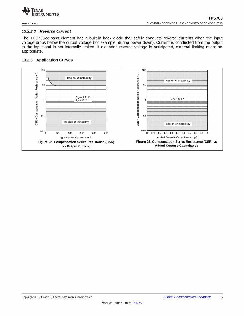
13.2.2.3 Reverse CurrentThe TPS763xx pass element has a built-in back diode that safely conducts reverse currents when the inputvoltage drops below the output voltage (for example, during power down). Current is conducted from the outputto the input and is not internally limited. If extended reverse voltage is anticipated, external limiting might beappropriate.
13.2.3 Application Curves
Figure 22. Compensation Series Resistance (CSR)vs Output Current
Figure 23. Compensation Series Resistance (CSR) vsAdded Ceramic Capacitance
COUT
VOUTVIN
GND PLANE
CIN
Represents via used for application specific connections
1
2
3 4
5
D I O OP (V V ) I= - ´
J AD(max)
JA
T max TP
Rq
-=
16
TPS763SLVS181I –DECEMBER 1998–REVISED DECEMBER 2016 www.ti.com
Product Folder Links: TPS763
Submit Documentation Feedback Copyright © 1998–2016, Texas Instruments Incorporated
14 Power Supply RecommendationsA 1-µF or larger input capacitor must be used.
14.1 Power Dissipation and Junction TemperatureSpecified regulator operation is assured to a junction temperature of 125°C; the maximum junction temperatureallowable to avoid damaging the device is 150°C. This restriction limits the power dissipation the regulator canhandle in any given application. To ensure the junction temperature is within acceptable limits, calculate themaximum allowable dissipation, PD(max), and the actual dissipation, PD, which must be less than or equal toPD(max).
The maximum-power-dissipation limit is determined using Equation 3.
where• TJmax is the maximum allowable junction temperature• RθJA is the thermal resistance junction-to-ambient for the package, see Thermal Information• TA is the ambient temperature (3)
The regulator dissipation is calculating using Equation 4.(4)
Power dissipation resulting from quiescent current is negligible.
15 Layout
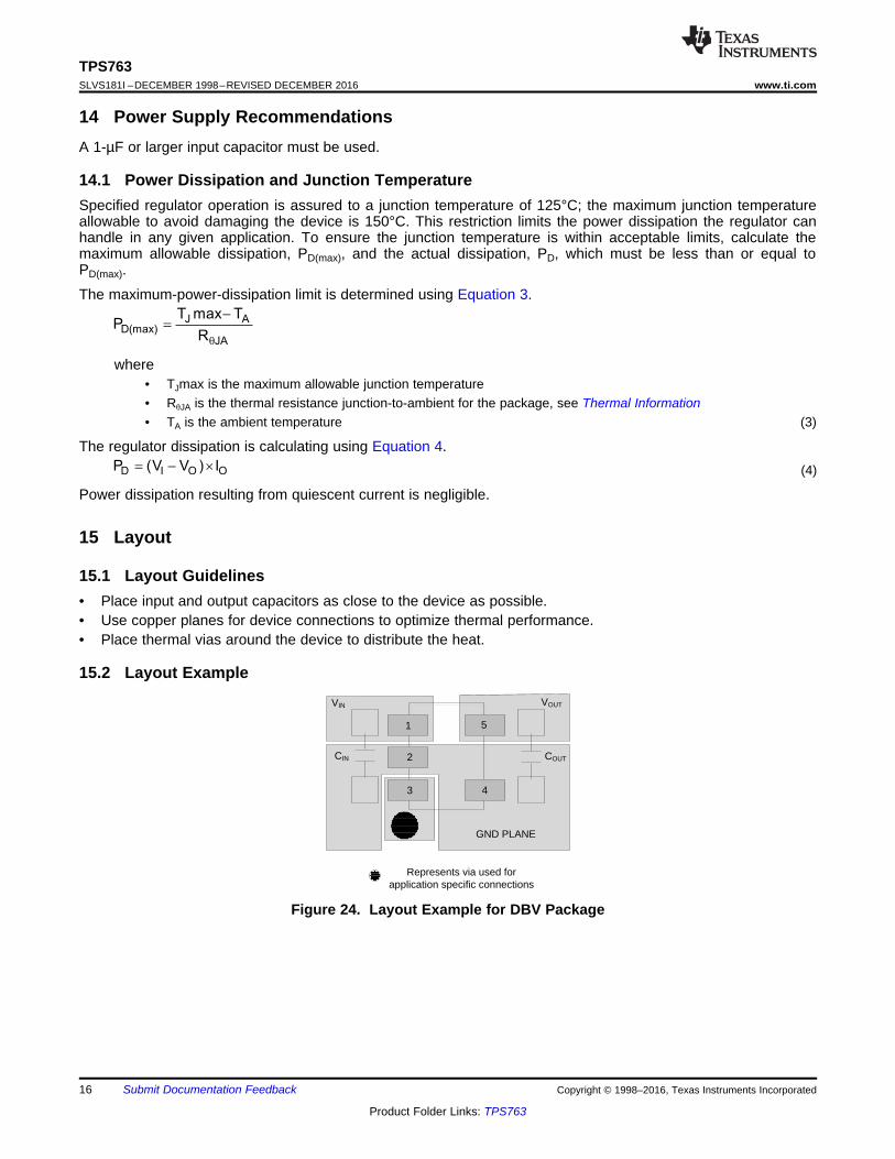
15.1 Layout Guidelines• Place input and output capacitors as close to the device as possible.• Use copper planes for device connections to optimize thermal performance.• Place thermal vias around the device to distribute the heat.
15.2 Layout Example
Figure 24. Layout Example for DBV Package
17
TPS763www.ti.com SLVS181I –DECEMBER 1998–REVISED DECEMBER 2016
Product Folder Links: TPS763
Submit Documentation FeedbackCopyright © 1998–2016, Texas Instruments Incorporated
16 Device and Documentation Support
16.1 Receiving Notification of Documentation UpdatesTo receive notification of documentation updates, navigate to the device product folder on ti.com. In the upperright corner, click on Alert me to register and receive a weekly digest of any product information that haschanged. For change details, review the revision history included in any revised document.
16.2 Community ResourcesThe following links connect to TI community resources. Linked contents are provided "AS IS" by the respectivecontributors. They do not constitute TI specifications and do not necessarily reflect TI's views; see TI's Terms ofUse.
TI E2E™ Online Community TI's Engineer-to-Engineer (E2E) Community. Created to foster collaborationamong engineers. At e2e.ti.com, you can ask questions, share knowledge, explore ideas and helpsolve problems with fellow engineers.
Design Support TI's Design Support Quickly find helpful E2E forums along with design support tools andcontact information for technical support.
16.3 TrademarksE2E is a trademark of Texas Instruments.All other trademarks are the property of their respective owners.
16.4 Electrostatic Discharge CautionThese devices have limited built-in ESD protection. The leads should be shorted together or the device placed in conductive foamduring storage or handling to prevent electrostatic damage to the MOS gates.
16.5 GlossarySLYZ022 — TI Glossary.
This glossary lists and explains terms, acronyms, and definitions.
17 Mechanical, Packaging, and Orderable InformationThe following pages include mechanical, packaging, and orderable information. This information is the mostcurrent data available for the designated devices. This data is subject to change without notice and revision ofthis document. For browser-based versions of this data sheet, refer to the left-hand navigation.
PACKAGE OPTION ADDENDUM
www.ti.com 17-Mar-2017
Addendum-Page 1
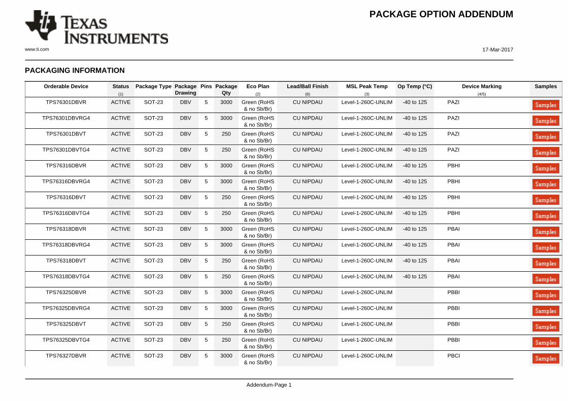
PACKAGING INFORMATION
Orderable Device Status(1)
Package Type PackageDrawing
Pins PackageQty
Eco Plan(2)
Lead/Ball Finish(6)
MSL Peak Temp(3)
Op Temp (°C) Device Marking(4/5)
Samples
TPS76301DBVR ACTIVE SOT-23 DBV 5 3000 Green (RoHS& no Sb/Br)
CU NIPDAU Level-1-260C-UNLIM -40 to 125 PAZI
TPS76301DBVRG4 ACTIVE SOT-23 DBV 5 3000 Green (RoHS& no Sb/Br)
CU NIPDAU Level-1-260C-UNLIM -40 to 125 PAZI
TPS76301DBVT ACTIVE SOT-23 DBV 5 250 Green (RoHS& no Sb/Br)
CU NIPDAU Level-1-260C-UNLIM -40 to 125 PAZI
TPS76301DBVTG4 ACTIVE SOT-23 DBV 5 250 Green (RoHS& no Sb/Br)
CU NIPDAU Level-1-260C-UNLIM -40 to 125 PAZI
TPS76316DBVR ACTIVE SOT-23 DBV 5 3000 Green (RoHS& no Sb/Br)
CU NIPDAU Level-1-260C-UNLIM -40 to 125 PBHI
TPS76316DBVRG4 ACTIVE SOT-23 DBV 5 3000 Green (RoHS& no Sb/Br)
CU NIPDAU Level-1-260C-UNLIM -40 to 125 PBHI
TPS76316DBVT ACTIVE SOT-23 DBV 5 250 Green (RoHS& no Sb/Br)
CU NIPDAU Level-1-260C-UNLIM -40 to 125 PBHI
TPS76316DBVTG4 ACTIVE SOT-23 DBV 5 250 Green (RoHS& no Sb/Br)
CU NIPDAU Level-1-260C-UNLIM -40 to 125 PBHI
TPS76318DBVR ACTIVE SOT-23 DBV 5 3000 Green (RoHS& no Sb/Br)
CU NIPDAU Level-1-260C-UNLIM -40 to 125 PBAI
TPS76318DBVRG4 ACTIVE SOT-23 DBV 5 3000 Green (RoHS& no Sb/Br)
CU NIPDAU Level-1-260C-UNLIM -40 to 125 PBAI
TPS76318DBVT ACTIVE SOT-23 DBV 5 250 Green (RoHS& no Sb/Br)
CU NIPDAU Level-1-260C-UNLIM -40 to 125 PBAI
TPS76318DBVTG4 ACTIVE SOT-23 DBV 5 250 Green (RoHS& no Sb/Br)
CU NIPDAU Level-1-260C-UNLIM -40 to 125 PBAI
TPS76325DBVR ACTIVE SOT-23 DBV 5 3000 Green (RoHS& no Sb/Br)
CU NIPDAU Level-1-260C-UNLIM PBBI
TPS76325DBVRG4 ACTIVE SOT-23 DBV 5 3000 Green (RoHS& no Sb/Br)
CU NIPDAU Level-1-260C-UNLIM PBBI
TPS76325DBVT ACTIVE SOT-23 DBV 5 250 Green (RoHS& no Sb/Br)
CU NIPDAU Level-1-260C-UNLIM PBBI
TPS76325DBVTG4 ACTIVE SOT-23 DBV 5 250 Green (RoHS& no Sb/Br)
CU NIPDAU Level-1-260C-UNLIM PBBI
TPS76327DBVR ACTIVE SOT-23 DBV 5 3000 Green (RoHS& no Sb/Br)
CU NIPDAU Level-1-260C-UNLIM PBCI
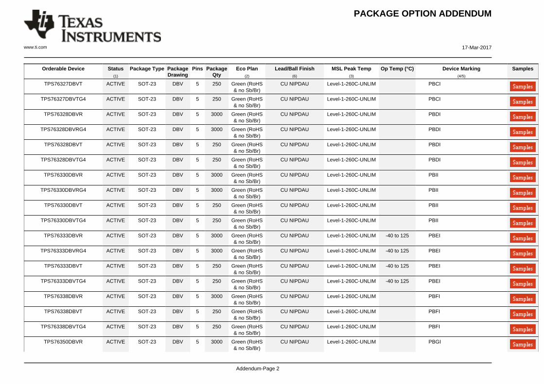
PACKAGE OPTION ADDENDUM
www.ti.com 17-Mar-2017
Addendum-Page 2
Orderable Device Status(1)
Package Type PackageDrawing
Pins PackageQty
Eco Plan(2)
Lead/Ball Finish(6)
MSL Peak Temp(3)
Op Temp (°C) Device Marking(4/5)
Samples
TPS76327DBVT ACTIVE SOT-23 DBV 5 250 Green (RoHS& no Sb/Br)
CU NIPDAU Level-1-260C-UNLIM PBCI
TPS76327DBVTG4 ACTIVE SOT-23 DBV 5 250 Green (RoHS& no Sb/Br)
CU NIPDAU Level-1-260C-UNLIM PBCI
TPS76328DBVR ACTIVE SOT-23 DBV 5 3000 Green (RoHS& no Sb/Br)
CU NIPDAU Level-1-260C-UNLIM PBDI
TPS76328DBVRG4 ACTIVE SOT-23 DBV 5 3000 Green (RoHS& no Sb/Br)
CU NIPDAU Level-1-260C-UNLIM PBDI
TPS76328DBVT ACTIVE SOT-23 DBV 5 250 Green (RoHS& no Sb/Br)
CU NIPDAU Level-1-260C-UNLIM PBDI
TPS76328DBVTG4 ACTIVE SOT-23 DBV 5 250 Green (RoHS& no Sb/Br)
CU NIPDAU Level-1-260C-UNLIM PBDI
TPS76330DBVR ACTIVE SOT-23 DBV 5 3000 Green (RoHS& no Sb/Br)
CU NIPDAU Level-1-260C-UNLIM PBII
TPS76330DBVRG4 ACTIVE SOT-23 DBV 5 3000 Green (RoHS& no Sb/Br)
CU NIPDAU Level-1-260C-UNLIM PBII
TPS76330DBVT ACTIVE SOT-23 DBV 5 250 Green (RoHS& no Sb/Br)
CU NIPDAU Level-1-260C-UNLIM PBII
TPS76330DBVTG4 ACTIVE SOT-23 DBV 5 250 Green (RoHS& no Sb/Br)
CU NIPDAU Level-1-260C-UNLIM PBII
TPS76333DBVR ACTIVE SOT-23 DBV 5 3000 Green (RoHS& no Sb/Br)
CU NIPDAU Level-1-260C-UNLIM -40 to 125 PBEI
TPS76333DBVRG4 ACTIVE SOT-23 DBV 5 3000 Green (RoHS& no Sb/Br)
CU NIPDAU Level-1-260C-UNLIM -40 to 125 PBEI
TPS76333DBVT ACTIVE SOT-23 DBV 5 250 Green (RoHS& no Sb/Br)
CU NIPDAU Level-1-260C-UNLIM -40 to 125 PBEI
TPS76333DBVTG4 ACTIVE SOT-23 DBV 5 250 Green (RoHS& no Sb/Br)
CU NIPDAU Level-1-260C-UNLIM -40 to 125 PBEI
TPS76338DBVR ACTIVE SOT-23 DBV 5 3000 Green (RoHS& no Sb/Br)
CU NIPDAU Level-1-260C-UNLIM PBFI
TPS76338DBVT ACTIVE SOT-23 DBV 5 250 Green (RoHS& no Sb/Br)
CU NIPDAU Level-1-260C-UNLIM PBFI
TPS76338DBVTG4 ACTIVE SOT-23 DBV 5 250 Green (RoHS& no Sb/Br)
CU NIPDAU Level-1-260C-UNLIM PBFI
TPS76350DBVR ACTIVE SOT-23 DBV 5 3000 Green (RoHS& no Sb/Br)
CU NIPDAU Level-1-260C-UNLIM PBGI
PACKAGE OPTION ADDENDUM
www.ti.com 17-Mar-2017
Addendum-Page 3
Orderable Device Status(1)
Package Type PackageDrawing
Pins PackageQty
Eco Plan(2)
Lead/Ball Finish(6)
MSL Peak Temp(3)
Op Temp (°C) Device Marking(4/5)
Samples
TPS76350DBVRG4 ACTIVE SOT-23 DBV 5 3000 Green (RoHS& no Sb/Br)
CU NIPDAU Level-1-260C-UNLIM PBGI
TPS76350DBVT ACTIVE SOT-23 DBV 5 250 Green (RoHS& no Sb/Br)
CU NIPDAU Level-1-260C-UNLIM PBGI
TPS76350DBVTG4 ACTIVE SOT-23 DBV 5 250 Green (RoHS& no Sb/Br)
CU NIPDAU Level-1-260C-UNLIM PBGI
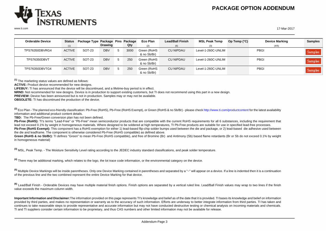
(1) The marketing status values are defined as follows:ACTIVE: Product device recommended for new designs.LIFEBUY: TI has announced that the device will be discontinued, and a lifetime-buy period is in effect.NRND: Not recommended for new designs. Device is in production to support existing customers, but TI does not recommend using this part in a new design.PREVIEW: Device has been announced but is not in production. Samples may or may not be available.OBSOLETE: TI has discontinued the production of the device.
(2) Eco Plan - The planned eco-friendly classification: Pb-Free (RoHS), Pb-Free (RoHS Exempt), or Green (RoHS & no Sb/Br) - please check http://www.ti.com/productcontent for the latest availabilityinformation and additional product content details.TBD: The Pb-Free/Green conversion plan has not been defined.Pb-Free (RoHS): TI's terms "Lead-Free" or "Pb-Free" mean semiconductor products that are compatible with the current RoHS requirements for all 6 substances, including the requirement thatlead not exceed 0.1% by weight in homogeneous materials. Where designed to be soldered at high temperatures, TI Pb-Free products are suitable for use in specified lead-free processes.Pb-Free (RoHS Exempt): This component has a RoHS exemption for either 1) lead-based flip-chip solder bumps used between the die and package, or 2) lead-based die adhesive used betweenthe die and leadframe. The component is otherwise considered Pb-Free (RoHS compatible) as defined above.Green (RoHS & no Sb/Br): TI defines "Green" to mean Pb-Free (RoHS compatible), and free of Bromine (Br) and Antimony (Sb) based flame retardants (Br or Sb do not exceed 0.1% by weightin homogeneous material)
(3) MSL, Peak Temp. - The Moisture Sensitivity Level rating according to the JEDEC industry standard classifications, and peak solder temperature.
(4) There may be additional marking, which relates to the logo, the lot trace code information, or the environmental category on the device.
(5) Multiple Device Markings will be inside parentheses. Only one Device Marking contained in parentheses and separated by a "~" will appear on a device. If a line is indented then it is a continuationof the previous line and the two combined represent the entire Device Marking for that device.
(6) Lead/Ball Finish - Orderable Devices may have multiple material finish options. Finish options are separated by a vertical ruled line. Lead/Ball Finish values may wrap to two lines if the finishvalue exceeds the maximum column width.
Important Information and Disclaimer:The information provided on this page represents TI's knowledge and belief as of the date that it is provided. TI bases its knowledge and belief on informationprovided by third parties, and makes no representation or warranty as to the accuracy of such information. Efforts are underway to better integrate information from third parties. TI has taken andcontinues to take reasonable steps to provide representative and accurate information but may not have conducted destructive testing or chemical analysis on incoming materials and chemicals.TI and TI suppliers consider certain information to be proprietary, and thus CAS numbers and other limited information may not be available for release.
PACKAGE OPTION ADDENDUM
www.ti.com 17-Mar-2017
Addendum-Page 4
In no event shall TI's liability arising out of such information exceed the total purchase price of the TI part(s) at issue in this document sold by TI to Customer on an annual basis.
OTHER QUALIFIED VERSIONS OF TPS763 :
• Automotive: TPS763-Q1
NOTE: Qualified Version Definitions:
• Automotive - Q100 devices qualified for high-reliability automotive applications targeting zero defects
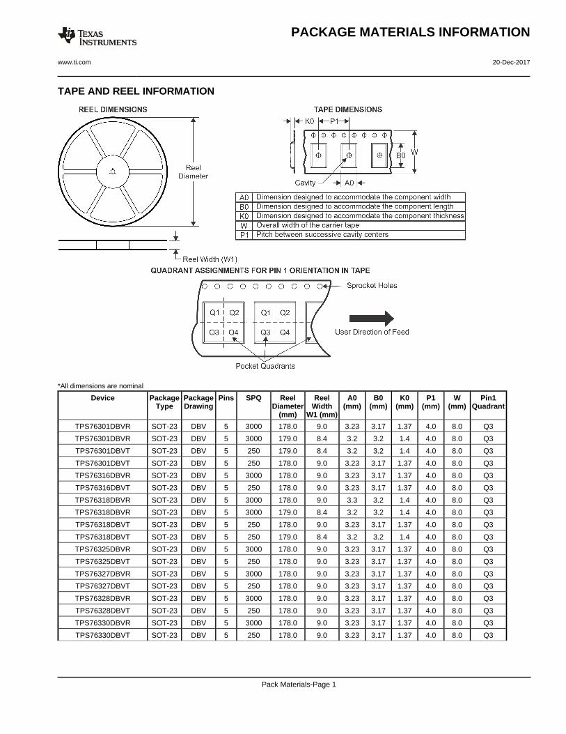
TAPE AND REEL INFORMATION
*All dimensions are nominal
Device PackageType
PackageDrawing
Pins SPQ ReelDiameter
(mm)
ReelWidth
W1 (mm)
A0(mm)
B0(mm)
K0(mm)
P1(mm)
W(mm)
Pin1Quadrant
TPS76301DBVR SOT-23 DBV 5 3000 178.0 9.0 3.23 3.17 1.37 4.0 8.0 Q3
TPS76301DBVR SOT-23 DBV 5 3000 179.0 8.4 3.2 3.2 1.4 4.0 8.0 Q3
TPS76301DBVT SOT-23 DBV 5 250 179.0 8.4 3.2 3.2 1.4 4.0 8.0 Q3
TPS76301DBVT SOT-23 DBV 5 250 178.0 9.0 3.23 3.17 1.37 4.0 8.0 Q3
TPS76316DBVR SOT-23 DBV 5 3000 178.0 9.0 3.23 3.17 1.37 4.0 8.0 Q3
TPS76316DBVT SOT-23 DBV 5 250 178.0 9.0 3.23 3.17 1.37 4.0 8.0 Q3
TPS76318DBVR SOT-23 DBV 5 3000 178.0 9.0 3.3 3.2 1.4 4.0 8.0 Q3
TPS76318DBVR SOT-23 DBV 5 3000 179.0 8.4 3.2 3.2 1.4 4.0 8.0 Q3
TPS76318DBVT SOT-23 DBV 5 250 178.0 9.0 3.23 3.17 1.37 4.0 8.0 Q3
TPS76318DBVT SOT-23 DBV 5 250 179.0 8.4 3.2 3.2 1.4 4.0 8.0 Q3
TPS76325DBVR SOT-23 DBV 5 3000 178.0 9.0 3.23 3.17 1.37 4.0 8.0 Q3
TPS76325DBVT SOT-23 DBV 5 250 178.0 9.0 3.23 3.17 1.37 4.0 8.0 Q3
TPS76327DBVR SOT-23 DBV 5 3000 178.0 9.0 3.23 3.17 1.37 4.0 8.0 Q3
TPS76327DBVT SOT-23 DBV 5 250 178.0 9.0 3.23 3.17 1.37 4.0 8.0 Q3
TPS76328DBVR SOT-23 DBV 5 3000 178.0 9.0 3.23 3.17 1.37 4.0 8.0 Q3
TPS76328DBVT SOT-23 DBV 5 250 178.0 9.0 3.23 3.17 1.37 4.0 8.0 Q3
TPS76330DBVR SOT-23 DBV 5 3000 178.0 9.0 3.23 3.17 1.37 4.0 8.0 Q3
TPS76330DBVT SOT-23 DBV 5 250 178.0 9.0 3.23 3.17 1.37 4.0 8.0 Q3
PACKAGE MATERIALS INFORMATION
www.ti.com 20-Dec-2017
Pack Materials-Page 1
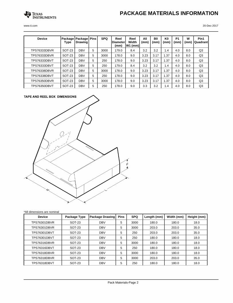
Device PackageType
PackageDrawing
Pins SPQ ReelDiameter
(mm)
ReelWidth
W1 (mm)
A0(mm)
B0(mm)
K0(mm)
P1(mm)
W(mm)
Pin1Quadrant
TPS76333DBVR SOT-23 DBV 5 3000 179.0 8.4 3.2 3.2 1.4 4.0 8.0 Q3
TPS76333DBVR SOT-23 DBV 5 3000 178.0 9.0 3.23 3.17 1.37 4.0 8.0 Q3
TPS76333DBVT SOT-23 DBV 5 250 178.0 9.0 3.23 3.17 1.37 4.0 8.0 Q3
TPS76333DBVT SOT-23 DBV 5 250 179.0 8.4 3.2 3.2 1.4 4.0 8.0 Q3
TPS76338DBVR SOT-23 DBV 5 3000 178.0 9.0 3.23 3.17 1.37 4.0 8.0 Q3
TPS76338DBVT SOT-23 DBV 5 250 178.0 9.0 3.23 3.17 1.37 4.0 8.0 Q3
TPS76350DBVR SOT-23 DBV 5 3000 178.0 9.0 3.23 3.17 1.37 4.0 8.0 Q3
TPS76350DBVT SOT-23 DBV 5 250 178.0 9.0 3.3 3.2 1.4 4.0 8.0 Q3
*All dimensions are nominal
Device Package Type Package Drawing Pins SPQ Length (mm) Width (mm) Height (mm)
TPS76301DBVR SOT-23 DBV 5 3000 180.0 180.0 18.0
TPS76301DBVR SOT-23 DBV 5 3000 203.0 203.0 35.0
TPS76301DBVT SOT-23 DBV 5 250 203.0 203.0 35.0
TPS76301DBVT SOT-23 DBV 5 250 180.0 180.0 18.0
TPS76316DBVR SOT-23 DBV 5 3000 180.0 180.0 18.0
TPS76316DBVT SOT-23 DBV 5 250 180.0 180.0 18.0
TPS76318DBVR SOT-23 DBV 5 3000 180.0 180.0 18.0
TPS76318DBVR SOT-23 DBV 5 3000 203.0 203.0 35.0
TPS76318DBVT SOT-23 DBV 5 250 180.0 180.0 18.0
PACKAGE MATERIALS INFORMATION
www.ti.com 20-Dec-2017
Pack Materials-Page 2
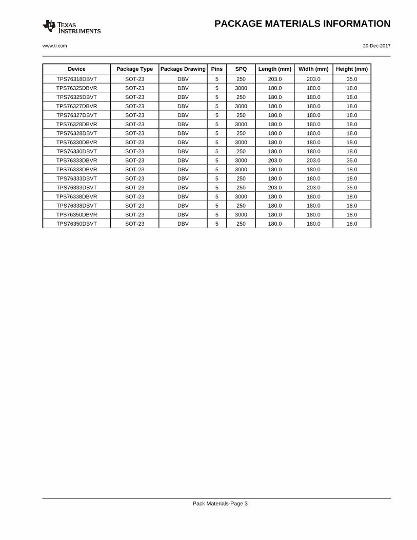
Device Package Type Package Drawing Pins SPQ Length (mm) Width (mm) Height (mm)
TPS76318DBVT SOT-23 DBV 5 250 203.0 203.0 35.0
TPS76325DBVR SOT-23 DBV 5 3000 180.0 180.0 18.0
TPS76325DBVT SOT-23 DBV 5 250 180.0 180.0 18.0
TPS76327DBVR SOT-23 DBV 5 3000 180.0 180.0 18.0
TPS76327DBVT SOT-23 DBV 5 250 180.0 180.0 18.0
TPS76328DBVR SOT-23 DBV 5 3000 180.0 180.0 18.0
TPS76328DBVT SOT-23 DBV 5 250 180.0 180.0 18.0
TPS76330DBVR SOT-23 DBV 5 3000 180.0 180.0 18.0
TPS76330DBVT SOT-23 DBV 5 250 180.0 180.0 18.0
TPS76333DBVR SOT-23 DBV 5 3000 203.0 203.0 35.0
TPS76333DBVR SOT-23 DBV 5 3000 180.0 180.0 18.0
TPS76333DBVT SOT-23 DBV 5 250 180.0 180.0 18.0
TPS76333DBVT SOT-23 DBV 5 250 203.0 203.0 35.0
TPS76338DBVR SOT-23 DBV 5 3000 180.0 180.0 18.0
TPS76338DBVT SOT-23 DBV 5 250 180.0 180.0 18.0
TPS76350DBVR SOT-23 DBV 5 3000 180.0 180.0 18.0
TPS76350DBVT SOT-23 DBV 5 250 180.0 180.0 18.0
PACKAGE MATERIALS INFORMATION
www.ti.com 20-Dec-2017
Pack Materials-Page 3
www.ti.com
PACKAGE OUTLINE
C
TYP0.220.08
0.25
3.02.6
2X 0.95
1.9
1.45 MAX
TYP0.150.00
5X 0.50.3
TYP0.60.3
TYP80
1.9
A
3.052.75
B1.751.45
(1.1)
SOT-23 - 1.45 mm max heightDBV0005ASMALL OUTLINE TRANSISTOR
4214839/C 04/2017
NOTES: 1. All linear dimensions are in millimeters. Any dimensions in parenthesis are for reference only. Dimensioning and tolerancing per ASME Y14.5M.2. This drawing is subject to change without notice.3. Refernce JEDEC MO-178.
0.2 C A B
1
34
5
2
INDEX AREAPIN 1
GAGE PLANE
SEATING PLANE
0.1 C
SCALE 4.000
www.ti.com
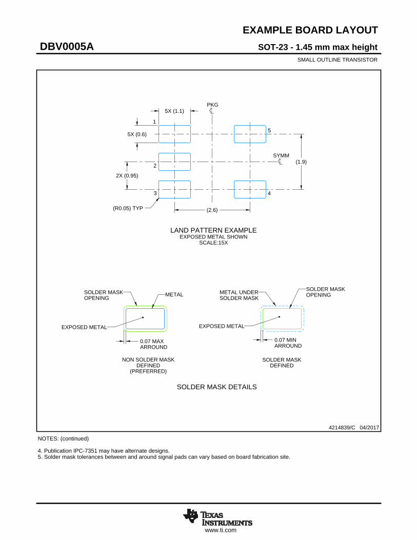
EXAMPLE BOARD LAYOUT
0.07 MAXARROUND
0.07 MINARROUND
5X (1.1)
5X (0.6)
(2.6)
(1.9)
2X (0.95)
(R0.05) TYP
4214839/C 04/2017
SOT-23 - 1.45 mm max heightDBV0005ASMALL OUTLINE TRANSISTOR
NOTES: (continued) 4. Publication IPC-7351 may have alternate designs. 5. Solder mask tolerances between and around signal pads can vary based on board fabrication site.
SYMM
LAND PATTERN EXAMPLEEXPOSED METAL SHOWN
SCALE:15X
PKG
1
3 4
5
2
SOLDER MASKOPENINGMETAL UNDER
SOLDER MASK
SOLDER MASKDEFINED
EXPOSED METAL
METALSOLDER MASKOPENING
NON SOLDER MASKDEFINED
(PREFERRED)
SOLDER MASK DETAILS
EXPOSED METAL
www.ti.com
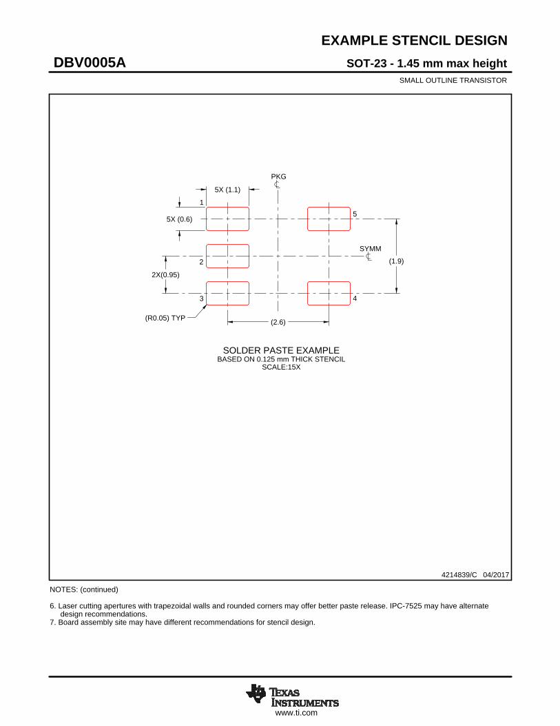
EXAMPLE STENCIL DESIGN
(2.6)
(1.9)
2X(0.95)
5X (1.1)
5X (0.6)
(R0.05) TYP
SOT-23 - 1.45 mm max heightDBV0005ASMALL OUTLINE TRANSISTOR
4214839/C 04/2017
NOTES: (continued) 6. Laser cutting apertures with trapezoidal walls and rounded corners may offer better paste release. IPC-7525 may have alternate design recommendations. 7. Board assembly site may have different recommendations for stencil design.
SOLDER PASTE EXAMPLEBASED ON 0.125 mm THICK STENCIL
SCALE:15X
SYMM
PKG
1
3 4
5
2
IMPORTANT NOTICE
Texas Instruments Incorporated (TI) reserves the right to make corrections, enhancements, improvements and other changes to itssemiconductor products and services per JESD46, latest issue, and to discontinue any product or service per JESD48, latest issue. Buyersshould obtain the latest relevant information before placing orders and should verify that such information is current and complete.TI’s published terms of sale for semiconductor products (http://www.ti.com/sc/docs/stdterms.htm) apply to the sale of packaged integratedcircuit products that TI has qualified and released to market. Additional terms may apply to the use or sale of other types of TI products andservices.Reproduction of significant portions of TI information in TI data sheets is permissible only if reproduction is without alteration and isaccompanied by all associated warranties, conditions, limitations, and notices. TI is not responsible or liable for such reproduceddocumentation. Information of third parties may be subject to additional restrictions. Resale of TI products or services with statementsdifferent from or beyond the parameters stated by TI for that product or service voids all express and any implied warranties for theassociated TI product or service and is an unfair and deceptive business practice. TI is not responsible or liable for any such statements.Buyers and others who are developing systems that incorporate TI products (collectively, “Designers”) understand and agree that Designersremain responsible for using their independent analysis, evaluation and judgment in designing their applications and that Designers havefull and exclusive responsibility to assure the safety of Designers' applications and compliance of their applications (and of all TI productsused in or for Designers’ applications) with all applicable regulations, laws and other applicable requirements. Designer represents that, withrespect to their applications, Designer has all the necessary expertise to create and implement safeguards that (1) anticipate dangerousconsequences of failures, (2) monitor failures and their consequences, and (3) lessen the likelihood of failures that might cause harm andtake appropriate actions. Designer agrees that prior to using or distributing any applications that include TI products, Designer willthoroughly test such applications and the functionality of such TI products as used in such applications.TI’s provision of technical, application or other design advice, quality characterization, reliability data or other services or information,including, but not limited to, reference designs and materials relating to evaluation modules, (collectively, “TI Resources”) are intended toassist designers who are developing applications that incorporate TI products; by downloading, accessing or using TI Resources in anyway, Designer (individually or, if Designer is acting on behalf of a company, Designer’s company) agrees to use any particular TI Resourcesolely for this purpose and subject to the terms of this Notice.TI’s provision of TI Resources does not expand or otherwise alter TI’s applicable published warranties or warranty disclaimers for TIproducts, and no additional obligations or liabilities arise from TI providing such TI Resources. TI reserves the right to make corrections,enhancements, improvements and other changes to its TI Resources. TI has not conducted any testing other than that specificallydescribed in the published documentation for a particular TI Resource.Designer is authorized to use, copy and modify any individual TI Resource only in connection with the development of applications thatinclude the TI product(s) identified in such TI Resource. NO OTHER LICENSE, EXPRESS OR IMPLIED, BY ESTOPPEL OR OTHERWISETO ANY OTHER TI INTELLECTUAL PROPERTY RIGHT, AND NO LICENSE TO ANY TECHNOLOGY OR INTELLECTUAL PROPERTYRIGHT OF TI OR ANY THIRD PARTY IS GRANTED HEREIN, including but not limited to any patent right, copyright, mask work right, orother intellectual property right relating to any combination, machine, or process in which TI products or services are used. Informationregarding or referencing third-party products or services does not constitute a license to use such products or services, or a warranty orendorsement thereof. Use of TI Resources may require a license from a third party under the patents or other intellectual property of thethird party, or a license from TI under the patents or other intellectual property of TI.TI RESOURCES ARE PROVIDED “AS IS” AND WITH ALL FAULTS. TI DISCLAIMS ALL OTHER WARRANTIES ORREPRESENTATIONS, EXPRESS OR IMPLIED, REGARDING RESOURCES OR USE THEREOF, INCLUDING BUT NOT LIMITED TOACCURACY OR COMPLETENESS, TITLE, ANY EPIDEMIC FAILURE WARRANTY AND ANY IMPLIED WARRANTIES OFMERCHANTABILITY, FITNESS FOR A PARTICULAR PURPOSE, AND NON-INFRINGEMENT OF ANY THIRD PARTY INTELLECTUALPROPERTY RIGHTS. TI SHALL NOT BE LIABLE FOR AND SHALL NOT DEFEND OR INDEMNIFY DESIGNER AGAINST ANY CLAIM,INCLUDING BUT NOT LIMITED TO ANY INFRINGEMENT CLAIM THAT RELATES TO OR IS BASED ON ANY COMBINATION OFPRODUCTS EVEN IF DESCRIBED IN TI RESOURCES OR OTHERWISE. IN NO EVENT SHALL TI BE LIABLE FOR ANY ACTUAL,DIRECT, SPECIAL, COLLATERAL, INDIRECT, PUNITIVE, INCIDENTAL, CONSEQUENTIAL OR EXEMPLARY DAMAGES INCONNECTION WITH OR ARISING OUT OF TI RESOURCES OR USE THEREOF, AND REGARDLESS OF WHETHER TI HAS BEENADVISED OF THE POSSIBILITY OF SUCH DAMAGES.Unless TI has explicitly designated an individual product as meeting the requirements of a particular industry standard (e.g., ISO/TS 16949and ISO 26262), TI is not responsible for any failure to meet such industry standard requirements.Where TI specifically promotes products as facilitating functional safety or as compliant with industry functional safety standards, suchproducts are intended to help enable customers to design and create their own applications that meet applicable functional safety standardsand requirements. Using products in an application does not by itself establish any safety features in the application. Designers mustensure compliance with safety-related requirements and standards applicable to their applications. Designer may not use any TI products inlife-critical medical equipment unless authorized officers of the parties have executed a special contract specifically governing such use.Life-critical medical equipment is medical equipment where failure of such equipment would cause serious bodily injury or death (e.g., lifesupport, pacemakers, defibrillators, heart pumps, neurostimulators, and implantables). Such equipment includes, without limitation, allmedical devices identified by the U.S. Food and Drug Administration as Class III devices and equivalent classifications outside the U.S.TI may expressly designate certain products as completing a particular qualification (e.g., Q100, Military Grade, or Enhanced Product).Designers agree that it has the necessary expertise to select the product with the appropriate qualification designation for their applicationsand that proper product selection is at Designers’ own risk. Designers are solely responsible for compliance with all legal and regulatoryrequirements in connection with such selection.Designer will fully indemnify TI and its representatives against any damages, costs, losses, and/or liabilities arising out of Designer’s non-compliance with the terms and provisions of this Notice.
Mailing Address: Texas Instruments, Post Office Box 655303, Dallas, Texas 75265Copyright © 2018, Texas Instruments Incorporated