Capacitance and Myelination vs. Conduction Velocity Mengqi Xing, Basheer Subei, Rafael Romero.
This is information on a product in full production.
June 2014 DocID025890 Rev 1 1/12
ESDAULC5-1BF4
Low clamping and ultra low capacitance single line bidirectionalESD protection
Datasheet - production data
Features• Low clamping voltage
• Bidirectional device
• Dynamic resistance Rd = 0.3 Ω typ.
• Low leakage current
• 0201 package size compatible
• Ultra small PCB area: 0.18 mm2
• ECOPACK®2 compliant component
Complies with the following standards
• IEC 61000-4-2 level 4:– ±30 kV (air discharge)– ±30 kV (contact discharge)
ApplicationsWhere transient over voltage protection in ESD sensitive equipment is required, such as:
• Smartphones, mobile phones and accessories
• Tablet, PC, netbooks and notebooks
• Portable multimedia devices and accessories
• Digital cameras and camcorders
• Communication and highly integrated systems
DescriptionThe ESDAULC5-1BF4 is a bidirectional single line TVS diode designed to protect the data line or other I/O ports against ESD transients.
The device is ideal for applications where both reduced line capacitance and board space saving are required.
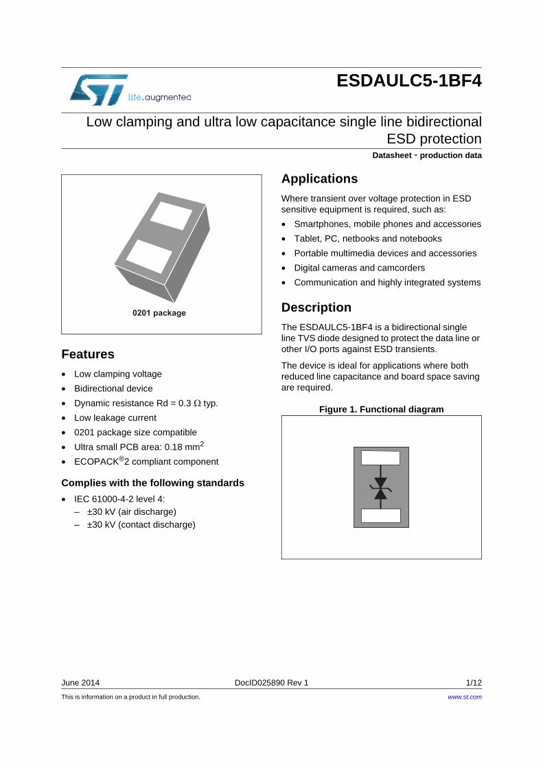
Figure 1. Functional diagram
0201 package
www.st.com
Characteristics ESDAULC5-1BF4
2/12 DocID025890 Rev 1
1 Characteristics
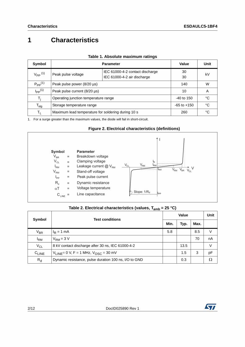
Figure 2. Electrical characteristics (definitions)
Table 1. Absolute maximum ratings
Symbol Parameter Value Unit
VPP (1) Peak pulse voltage
IEC 61000-4-2 contact dischargeIEC 61000-4-2 air discharge
3030
kV
PPP(1) Peak pulse power (8/20 µs) 140 W
IPP(1) Peak pulse current (8/20 µs) 10 A
Tj Operating junction temperature range -40 to 150 °C
Tstg Storage temperature range -65 to +150 °C
TL Maximum lead temperature for soldering during 10 s 260 °C
1. For a surge greater than the maximum values, the diode will fail in short-circuit.
Symbol Parameter
V = Breakdown voltage
I = Leakage current @ V
V = Stand-off voltage
I = Peak pulse current
R
BR
RM RM
RM
PP
V = Clamping voltageCL
d = Dynamic resistance
T = Voltage temperature
C = Line capacitanceLINE
V
V
IPPSlope: 1/Rd
CL
CL
Table 2. Electrical characteristics (values, Tamb = 25 °C)
Symbol Test conditionsValue Unit
Min. Typ. Max.
VBR IR = 1 mA 5.8 8.5 V
IRM VRM = 3 V 70 nA
VCL 8 kV contact discharge after 30 ns, IEC 61000-4-2 13.5 V
CLINE VLINE= 0 V, F = 1 MHz, VOSC = 30 mV 1.5 3 pF
Rd Dynamic resistance, pulse duration 100 ns, I/O to GND 0.3 Ω
DocID025890 Rev 1 3/12
ESDAULC5-1BF4 Characteristics
12
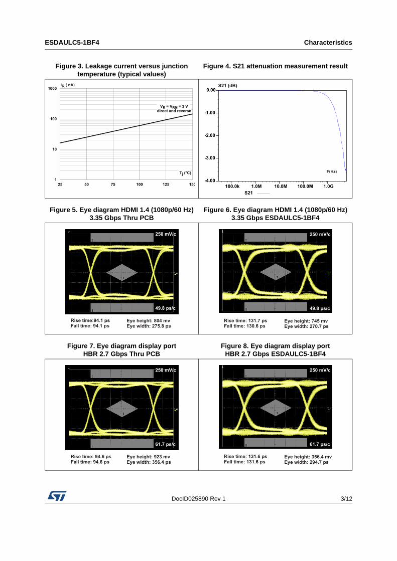
Figure 3. Leakage current versus junction temperature (typical values)
Figure 4. S21 attenuation measurement result
IR ( nA)
1
10
100
1000
25 50 75 100 125 150
V = V = 3 VR RMdirect and reverse
Tj °C( )
100.0k 1.0M 10.0M 100.0M 1.0G
-4.00
-3.00
-2.00
-1.00
0.00
S21
S21 (dB)
F(Hz)
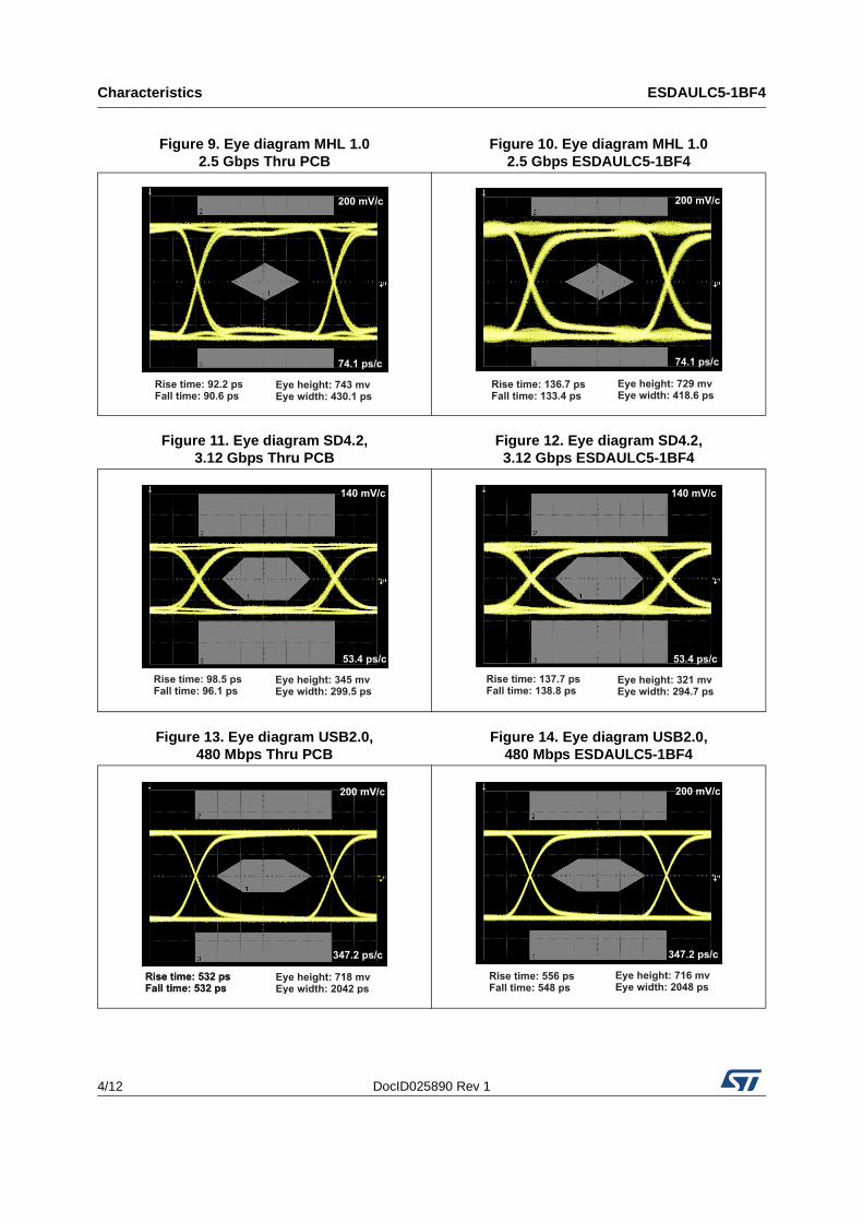
Figure 5. Eye diagram HDMI 1.4 (1080p/60 Hz) 3.35 Gbps Thru PCB
Figure 6. Eye diagram HDMI 1.4 (1080p/60 Hz) 3.35 Gbps ESDAULC5-1BF4
Rise time:94.1 psFall time: 94.1 ps
Eye height: 804 mvEye width: 275.8 ps
250 mV/c
49.8 ps/c
Rise time: 131.7 psFall time: 130.6 ps
Eye height: 745 mvEye width: 270.7 ps
250 mV/c
49.8 ps/c
Figure 7. Eye diagram display port HBR 2.7 Gbps Thru PCB
Figure 8. Eye diagram display port HBR 2.7 Gbps ESDAULC5-1BF4
Rise time: 94.6 psFall time: 94.6 ps
Eye height: 923 mvEye width: 356.4 ps
250 mV/c
61.7 ps/c
Rise time: 131.6 psFall time: 131.6 ps
Eye height: 356.4 mvEye width: 294.7 ps
250 mV/c
61.7 ps/c
Characteristics ESDAULC5-1BF4
4/12 DocID025890 Rev 1
Figure 9. Eye diagram MHL 1.0 2.5 Gbps Thru PCB
Figure 10. Eye diagram MHL 1.0 2.5 Gbps ESDAULC5-1BF4
Rise time: 92.2 psFall time: 90.6 ps
200 mV/c
74.1 ps/c
Eye height: 743 mvEye width: 430.1 ps
200 mV/c
74.1 ps/c
Rise time: 136.7 psFall time: 133.4 ps
Eye height: 729 mvEye width: 418.6 ps
Figure 11. Eye diagram SD4.2, 3.12 Gbps Thru PCB
Figure 12. Eye diagram SD4.2, 3.12 Gbps ESDAULC5-1BF4
Rise time: 98.5 psFall time: 96.1 ps
Eye height: 345 mvEye width: 299.5 ps
140 mV/c
53.4 ps/c
Rise time: 137.7 psFall time: 138.8 ps
Eye height: 321 mvEye width: 294.7 ps
140 mV/c
53.4 ps/c
Figure 13. Eye diagram USB2.0, 480 Mbps Thru PCB
Figure 14. Eye diagram USB2.0, 480 Mbps ESDAULC5-1BF4
Rise time: 532 psFall time: 532 ps
200 mV/c
347.2 ps/c
Rise time: 532 psFall time: 532 ps
Eye height: 718 mvEye width: 2042 ps
200 mV/c
347.2 ps/c
Rise time: 556 psFall time: 548 ps
Eye height: 716 mvEye width: 2048 ps
DocID025890 Rev 1 5/12
ESDAULC5-1BF4 Characteristics
12
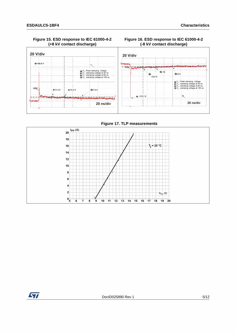
Figure 17. TLP measurements
Figure 15. ESD response to IEC 61000-4-2 (+8 kV contact discharge)
Figure 16. ESD response to IEC 61000-4-2 (-8 kV contact discharge)
20 V/div
7.5 V4
20 ns/div
V : Peak clamping voltageCL
V :clamping voltage at 30 nsCL
V :clamping voltage at 60 nsCL
V :clamping voltage at 100 nsCL
1234
1
11.3 V2 13.3 V32
106.8 V
-8 V4
20 ns/div
20 V/div
-1032
-12.4 V
1 -113.1 V
V : Peak clamping voltageCL
V :clamping voltage at 30 nsCL
V :clamping voltage at 60 nsCL
V :clamping voltage at 100 nsCL
1234
I (A)PP
0
2
4
6
8
10
12
14
16
18
20
5 6 7 8 9 10 11 12 13 14 15 16 17 18 19 20
V (V)CL
Tj = 25 °C
Package information ESDAULC5-1BF4
6/12 DocID025890 Rev 1
2 Package information
• Epoxy meets UL94, V0
• Lead-free package
In order to meet environmental requirements, ST offers these devices in different grades of ECOPACK® packages, depending on their level of environmental compliance. ECOPACK® specifications, grade definitions and product status are available at: www.st.com. ECOPACK® is an ST trademark.
Figure 18. 0201 package dimension definitions
Table 3. 0201 package dimension values
Ref.
Dimensions
Millimeters Inches
Min. Typ. Max. Min. Typ. Max.
A 0.28 0.3 0.32 0.0110 0.0118 0.0126
b 0.125 0.14 0.155 0.0049 0.0055 0.0061
D 0.57 0.6 0.63 0.0224 0.0236 0.0248
D1 0.35 0.0138
E 0.27 0.3 0.33 0.0106 0.0118 0.0130
E1 0.175 0.19 0.205 0.0069 0.0075 0.0081
fD 0.065 0.08 0.095 0.0026 0.0031 0.0037
fE 0.11 0.125 0.13 0.0043 0.0049 0.0051
Top
Bottom
Side
D
E
A
fD
fE
b
D1
E1
DocID025890 Rev 1 7/12
ESDAULC5-1BF4 Package information
12
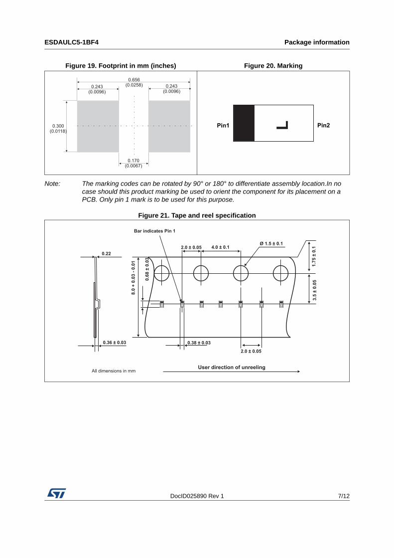
Note: The marking codes can be rotated by 90° or 180° to differentiate assembly location.In no case should this product marking be used to orient the component for its placement on a PCB. Only pin 1 mark is to be used for this purpose.
Figure 21. Tape and reel specification
Figure 19. Footprint in mm (inches) Figure 20. Marking
0.243(0.0096)
0.170(0.0067)
0.300(0.0118)
0.243(0.0096)
0.656(0.0258)
Pin1 Pin2L
Bar indicates Pin 1
User direction of unreelingAll dimensions in mm
4.0 ± 0.12.0 ± 0.05
8.0
+ 0
.03
- 0
.01
2.0 ± 0.05
1.7
5 ±
0.1
3.5
± 0
.05
Ø 1.5 ± 0.1
0.36 ± 0.03 0.38 ± 0.03
0.22
0.6
8 ±
0.0
3
5 5 55555
Recommendation on PCB assembly ESDAULC5-1BF4
8/12 DocID025890 Rev 1
3 Recommendation on PCB assembly
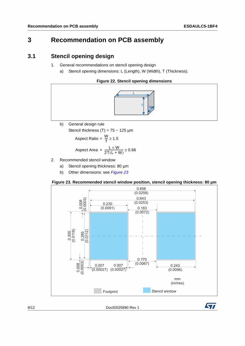
3.1 Stencil opening design1. General recommendations on stencil opening design
a) Stencil opening dimensions: L (Length), W (Width), T (Thickness).
Figure 22. Stencil opening dimensions
b) General design rule
Stencil thickness (T) = 75 ~ 125 µm
2. Recommended stencil window
a) Stencil opening thickness: 80 µm
b) Other dimensions: see Figure 23
Figure 23. Recommended stencil window position, stencil opening thickness: 80 µm
L
TW
Aspect Ratio WT----- 1.5≥=
Aspect AreaL W×
2T L W+( )---------------------------- 0.66≥=
0.230(0.0091) 0.183
(0.0072)
0.170(0.0067)
0.3
00
(0.0
118)
0.2
85
(0.0
112)
0.656(0.0258)
0.643(0.0253)
Footprint Stencil window
0.007(0.00027)
0.007(0.00027)0
.00
8(0
.00
03
)0
.00
8(0
.00
03
)
mm(inches)
0.243(0.0096)
DocID025890 Rev 1 9/12
ESDAULC5-1BF4 Recommendation on PCB assembly
12
3.2 Solder paste1. Use halide-free flux, qualification ROL0 according to ANSI/J-STD-004.
2. “No clean” solder paste recommended.
3. Offers a high tack force to resist component displacement during PCB movement.
4. Use solder paste with fine particles: Type 4 (powder particle size 20-48 µm per IPC J STD-005).
3.3 Placement1. Manual positioning is not recommended.
2. It is recommended to use the lead recognition capabilities of the placement system, not the outline centering.
3. Standard tolerance of ± 0.05 mm is recommended.
4. 1.0 N placement force is recommended. Too much placement force can lead to squeezed out solder paste and cause solder joints to short. Too low placement force can lead to insufficient contact between package and solder paste that could cause open solder joints or badly centered packages.
5. To improve the package placement accuracy, a bottom side optical control should be performed with a high resolution tool.
6. For assembly, a perfect supporting of the PCB (all the more on flexible PCB) is recommended during solder paste printing, pick and place and reflow soldering by using optimized tools.
3.4 PCB design preference1. To control the solder paste amount, the closed via is recommended instead of open
vias.
2. The position of tracks and open vias in the solder area should be well balanced. The symmetrical layout is recommended, in case any tilt phenomena caused by asymmetrical solder paste amount due to the solder flow away.
Recommendation on PCB assembly ESDAULC5-1BF4
10/12 DocID025890 Rev 1
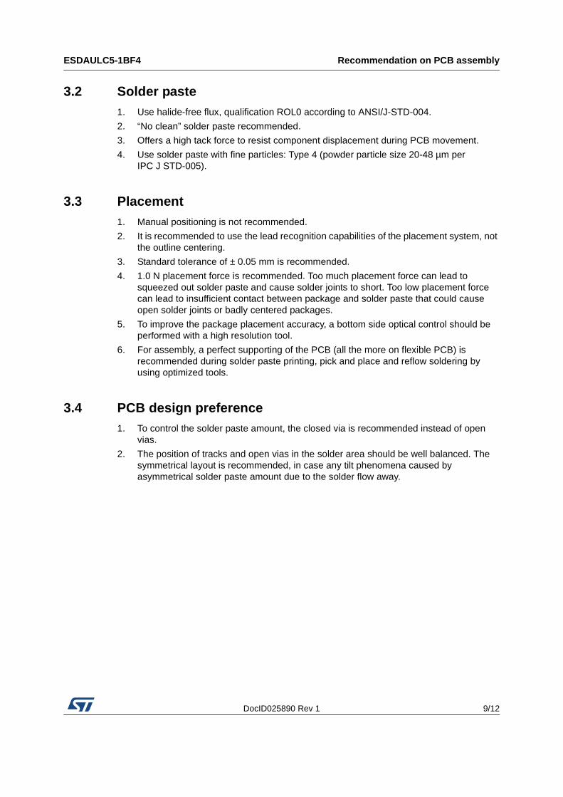
3.5 Reflow profile
Figure 24. ST ECOPACK® recommended soldering reflow profile for PCB mounting
Note: Minimize air convection currents in the reflow oven to avoid component movement.
250
0
50
100
150
200
240210180150120906030 300270
-6 °C/s
240-245 °C
2 - 3 °C/s
Temperature (°C)-2 °C/s
-3 °C/s
Time (s)
0.9 °C/s
60 sec(90 max)
DocID025890 Rev 1 11/12
ESDAULC5-1BF4 Ordering information
12
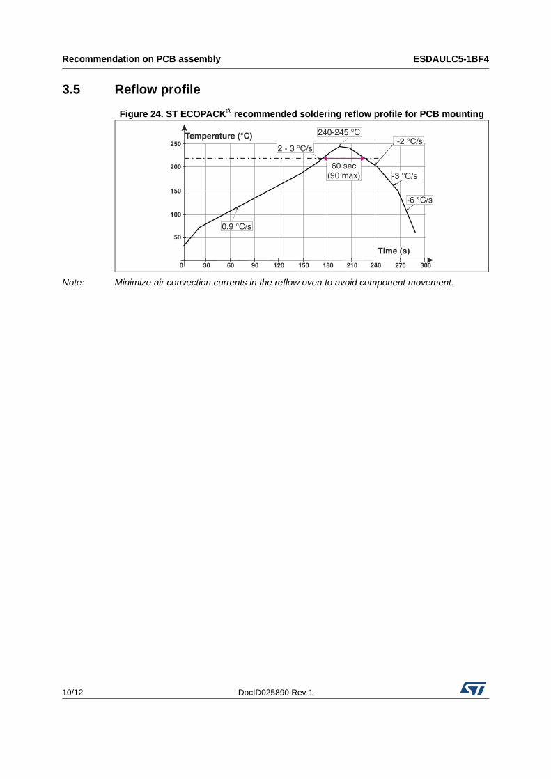
4 Ordering information
Figure 25. Ordering information scheme
5 Revision history
Table 4. Ordering information
Order code Marking Package Weight Base qty Delivery mode
ESDAULC5-1BF4 L(1)
1. The marking codes can be rotated by 90° or 180° to differentiate assembly location
0201 0.116 mg 15000 Tape and reel
ESDA - 1 BULC 5 F4
ESDA array
Ultra low capacitance
Breakdown voltage
5 = 5.8 V min
Number of lines
Directional
B = Bi-directional
Package
=F4 0201
Table 5. Document revision history
Date Revision Changes
03-Jun-2014 1 First issue.
ESDAULC5-1BF4
12/12 DocID025890 Rev 1
Please Read Carefully:
Information in this document is provided solely in connection with ST products. STMicroelectronics NV and its subsidiaries (“ST”) reserve theright to make changes, corrections, modifications or improvements, to this document, and the products and services described herein at anytime, without notice.
All ST products are sold pursuant to ST’s terms and conditions of sale.
Purchasers are solely responsible for the choice, selection and use of the ST products and services described herein, and ST assumes noliability whatsoever relating to the choice, selection or use of the ST products and services described herein.
No license, express or implied, by estoppel or otherwise, to any intellectual property rights is granted under this document. If any part of thisdocument refers to any third party products or services it shall not be deemed a license grant by ST for the use of such third party productsor services, or any intellectual property contained therein or considered as a warranty covering the use in any manner whatsoever of suchthird party products or services or any intellectual property contained therein.
UNLESS OTHERWISE SET FORTH IN ST’S TERMS AND CONDITIONS OF SALE ST DISCLAIMS ANY EXPRESS OR IMPLIED WARRANTY WITH RESPECT TO THE USE AND/OR SALE OF ST PRODUCTS INCLUDING WITHOUT LIMITATION IMPLIED WARRANTIES OF MERCHANTABILITY, FITNESS FOR A PARTICULAR PURPOSE (AND THEIR EQUIVALENTS UNDER THE LAWS OF ANY JURISDICTION), OR INFRINGEMENT OF ANY PATENT, COPYRIGHT OR OTHER INTELLECTUAL PROPERTY RIGHT.
ST PRODUCTS ARE NOT DESIGNED OR AUTHORIZED FOR USE IN: (A) SAFETY CRITICAL APPLICATIONS SUCH AS LIFE SUPPORTING, ACTIVE IMPLANTED DEVICES OR SYSTEMS WITH PRODUCT FUNCTIONAL SAFETY REQUIREMENTS; (B) AERONAUTIC APPLICATIONS; (C) AUTOMOTIVE APPLICATIONS OR ENVIRONMENTS, AND/OR (D) AEROSPACE APPLICATIONS OR ENVIRONMENTS. WHERE ST PRODUCTS ARE NOT DESIGNED FOR SUCH USE, THE PURCHASER SHALL USE PRODUCTS AT PURCHASER’S SOLE RISK, EVEN IF ST HAS BEEN INFORMED IN WRITING OF SUCH USAGE, UNLESS A PRODUCT IS EXPRESSLY DESIGNATED BY ST AS BEING INTENDED FOR “AUTOMOTIVE, AUTOMOTIVE SAFETY OR MEDICAL” INDUSTRY DOMAINS ACCORDING TO ST PRODUCT DESIGN SPECIFICATIONS. PRODUCTS FORMALLY ESCC, QML OR JAN QUALIFIED ARE DEEMED SUITABLE FOR USE IN AEROSPACE BY THE CORRESPONDING GOVERNMENTAL AGENCY.
Resale of ST products with provisions different from the statements and/or technical features set forth in this document shall immediately voidany warranty granted by ST for the ST product or service described herein and shall not create or extend in any manner whatsoever, anyliability of ST.
ST and the ST logo are trademarks or registered trademarks of ST in various countries.Information in this document supersedes and replaces all information previously supplied.
The ST logo is a registered trademark of STMicroelectronics. All other names are the property of their respective owners.
© 2014 STMicroelectronics - All rights reserved
STMicroelectronics group of companies
Australia - Belgium - Brazil - Canada - China - Czech Republic - Finland - France - Germany - Hong Kong - India - Israel - Italy - Japan - Malaysia - Malta - Morocco - Philippines - Singapore - Spain - Sweden - Switzerland - United Kingdom - United States of America
www.st.com