EE 330 Lecture 19 - Iowa State Universityclass.ece.iastate.edu/ee330/lectures/EE 330 Lect 19...
73
EE 330 Lecture 19 Bipolar Process Flow
Transcript of EE 330 Lecture 19 - Iowa State Universityclass.ece.iastate.edu/ee330/lectures/EE 330 Lect 19...

EE 330
Lecture 19
Bipolar Process Flow
Simplified Multi-Region Model
AF
CEBC
V
V1βII
t
BE
V
V
ESB e
β
AJI
q
kTVt
VBE=0.7V
VCE=0.2V
IC=IB=0
Forward Active
Saturation
Cutoff
VBE>0.4V
VBC<0
IC<βIB
VBE<0
VBC<0
A small portion of the operating region is missed with this model but seldom operate in
the missing region
0<IB
Review from Last Lecture

Further Simplified Multi-Region dc Model
Equivalent Simplified Multi-Region Model
C BI βI
BEV 0.6V
q
kTVt
VBE=0.7V
VCE=0.2V
IC=IB=0
Forward Active
Saturation
Cutoff
VBE>0.4V
VBC<0
IC<βIB
VBE<0
VBC<0
A small portion of the operating region is missed with this model but seldom operate in
the missing region
Review from Last Lecture
0<IB

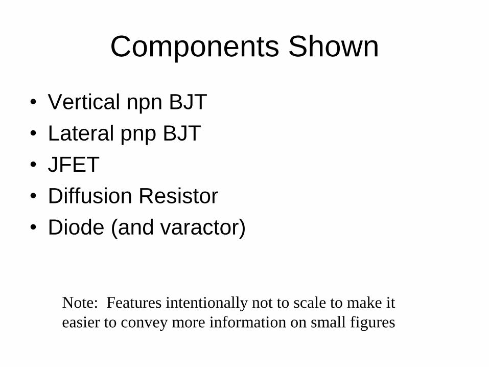
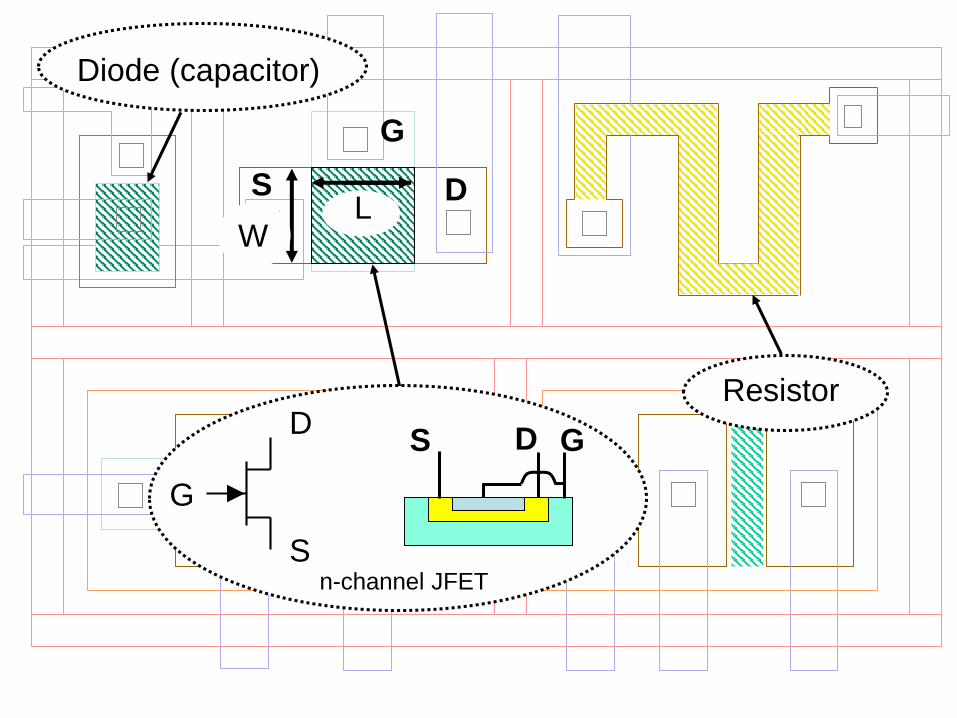
Bipolar Process Description
p-substrate epi
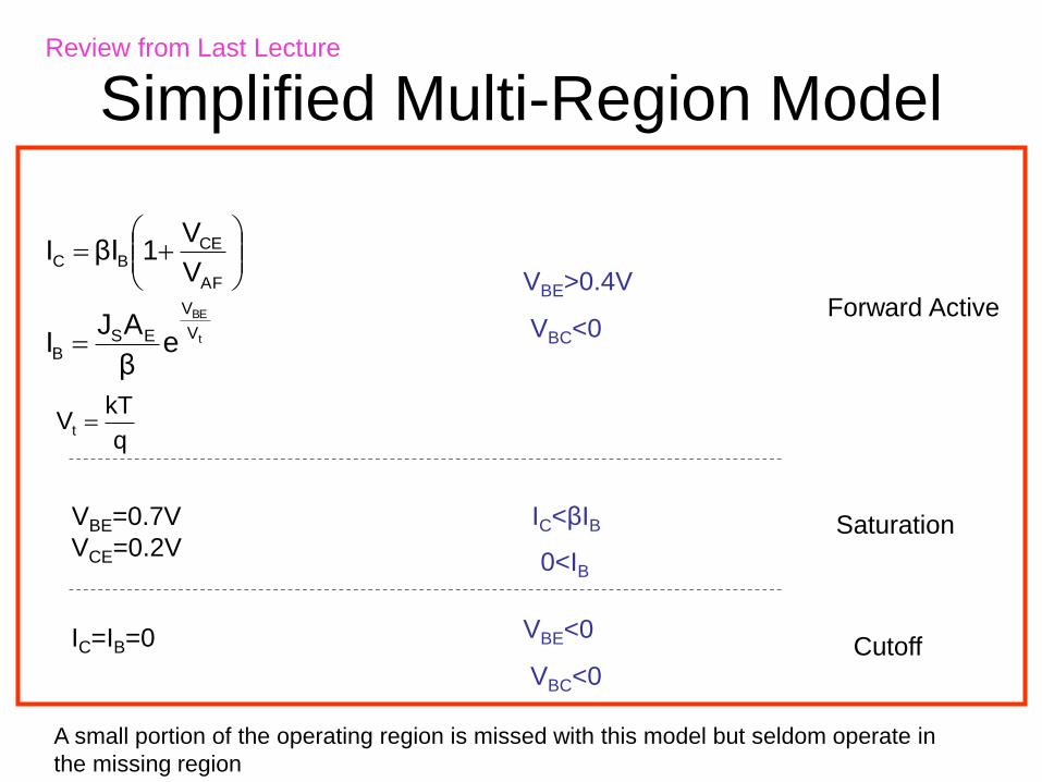
Components Shown
• Vertical npn BJT
• Lateral pnp BJT
• JFET
• Diffusion Resistor
• Diode (and varactor)
Note: Features intentionally not to scale to make it
easier to convey more information on small figures


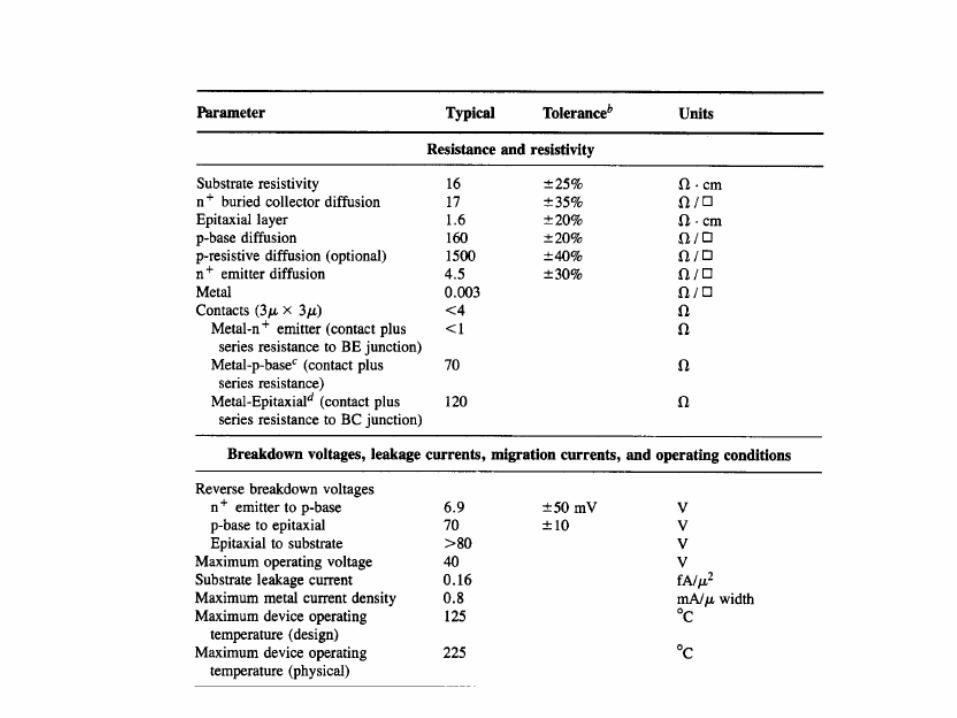
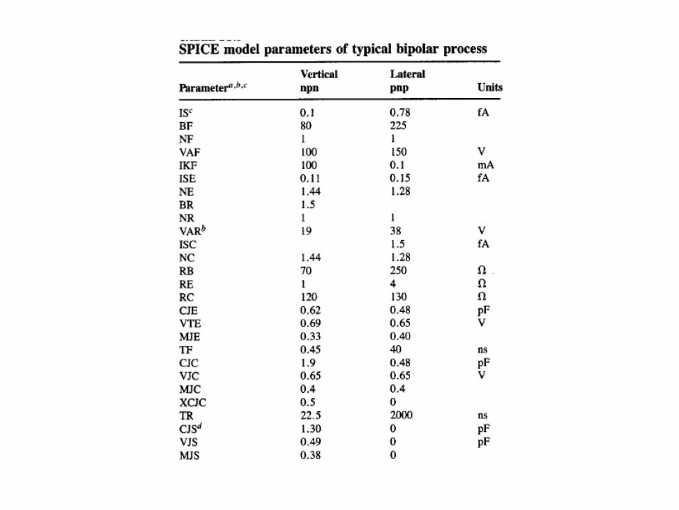
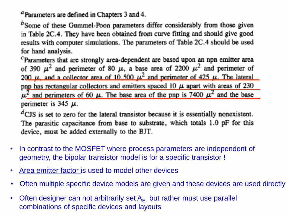
• In contrast to the MOSFET where process parameters are independent of
geometry, the bipolar transistor model is for a specific transistor !
• Area emitter factor is used to model other devices
• Often multiple specific device models are given and these devices are used directly
• Often designer can not arbitrarily set AE but rather must use parallel
combinations of specific devices and layouts
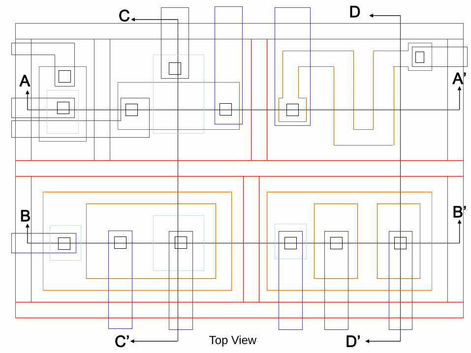
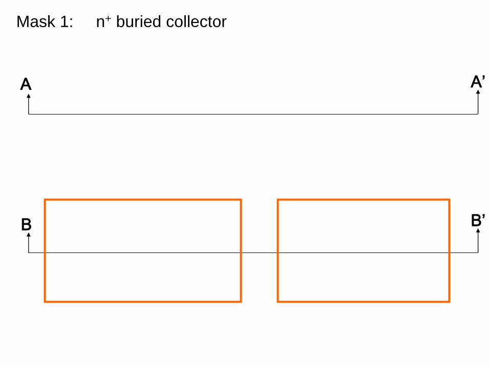
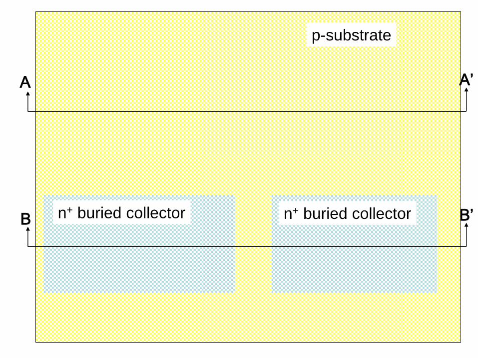
A A’
B’B
C
C’
D
D’Top View
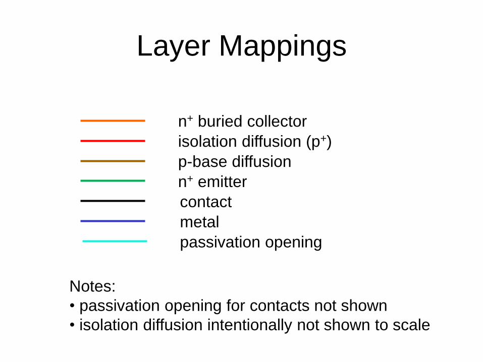
Layer Mappings
n+ buried collector
isolation diffusion (p+)
p-base diffusion
n+ emitter
contact
metal
passivation opening
Notes:
• passivation opening for contacts not shown
• isolation diffusion intentionally not shown to scale
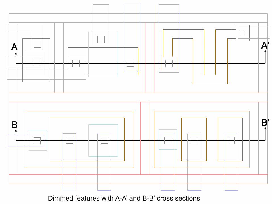
A A’
B’B
Dimmed features with A-A’ and B-B’ cross sections
A A’
B’B

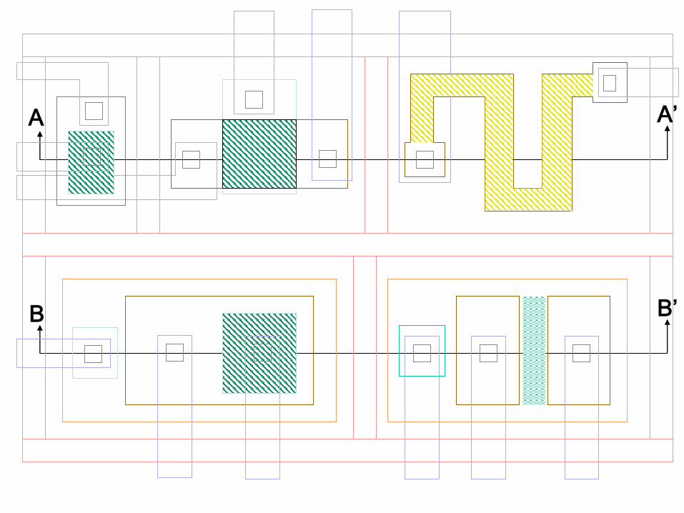
BE
C
E
B
C
EC Blateral pnp
E
C
B
vertical npn
B
C
E
E C
B

L
G
DS
Resistor
Diode (capacitor)
GDS
S
D
G
n-channel JFET
W

Detailed Description of First
Photolithographic Steps Only
• Top View
• Cross-Section View
A A’
B’B
n+ buried collector
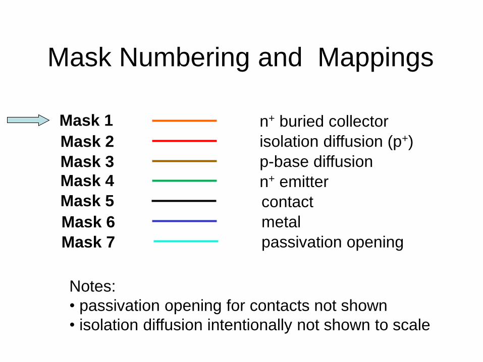
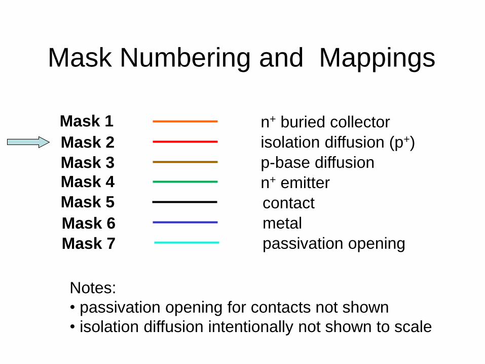
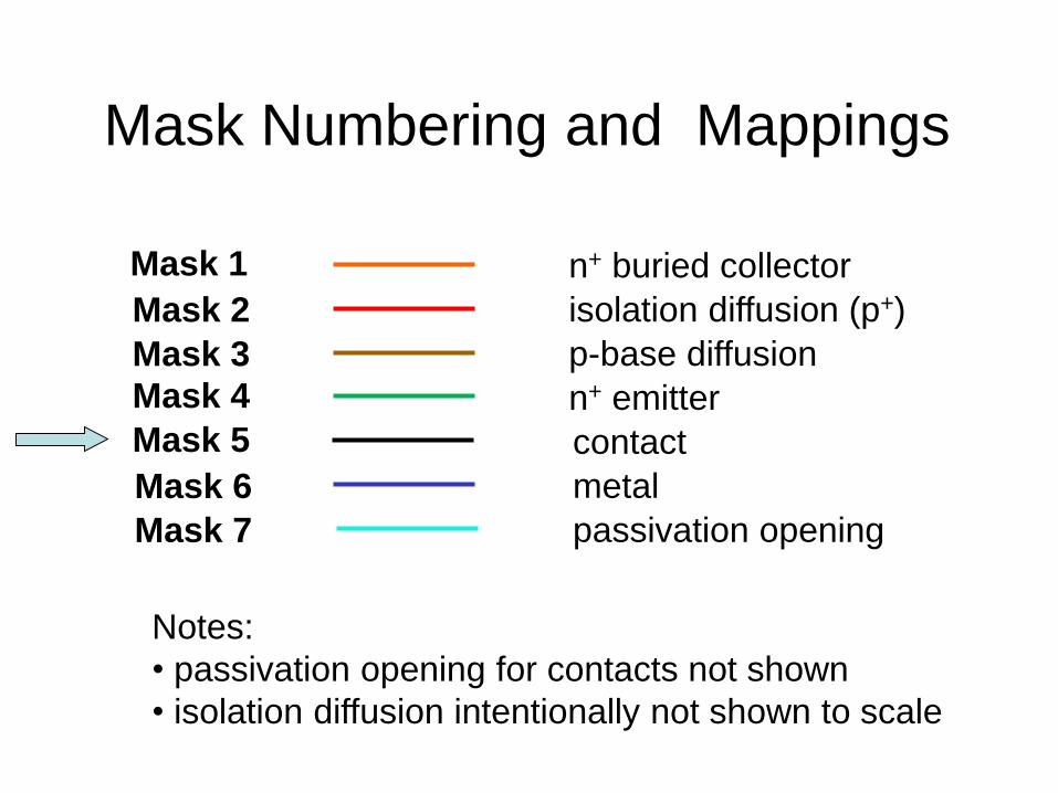
Mask Numbering and Mappings
n+ buried collector
isolation diffusion (p+)
p-base diffusion
n+ emitter
contact
metal
passivation opening
Notes:
• passivation opening for contacts not shown
• isolation diffusion intentionally not shown to scale
Mask 1
Mask 2
Mask 3
Mask 4
Mask 5
Mask 6
Mask 7
A A’
B’B
Mask 1: n+ buried collector
A-A’ Section
B-B’ Section
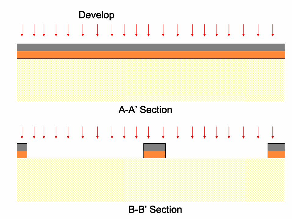
Photoresistn+ buried collector maskExposureDevelop
A-A’ Section
B-B’ Section
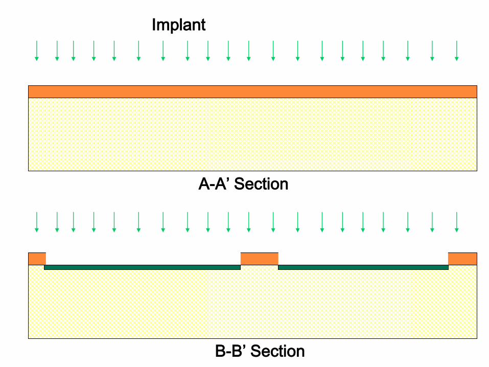
Implant

A-A’ Section
B-B’ Section
Strip Photoresist
A A’
B’B
p-substrate
n+ buried collector n+ buried collector
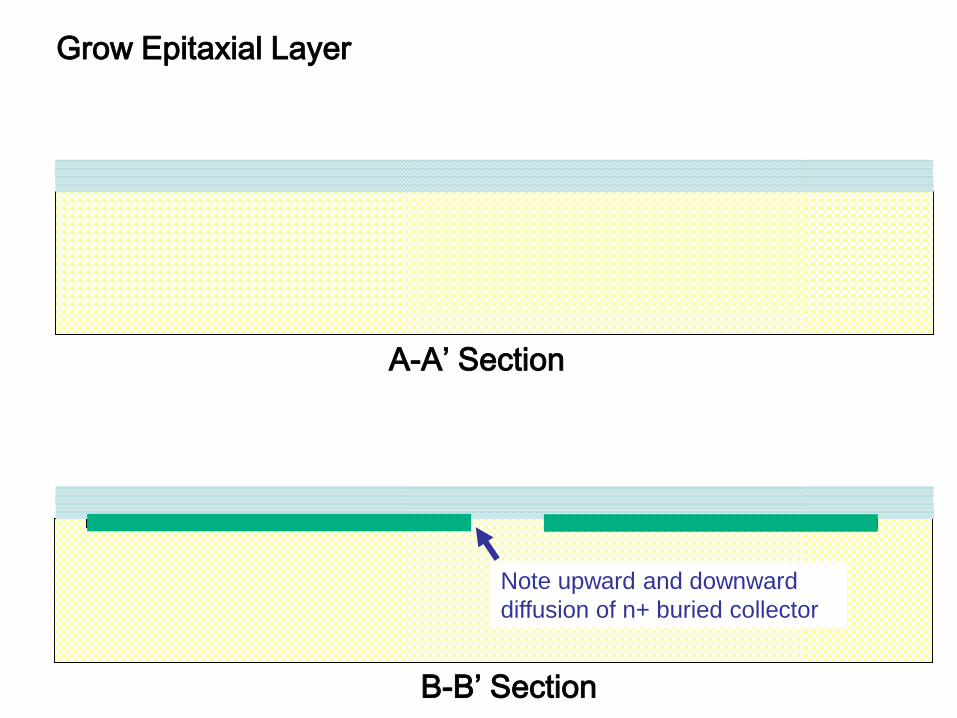
A-A’ Section
B-B’ Section
Grow Epitaxial Layer
Note upward and downward
diffusion of n+ buried collector
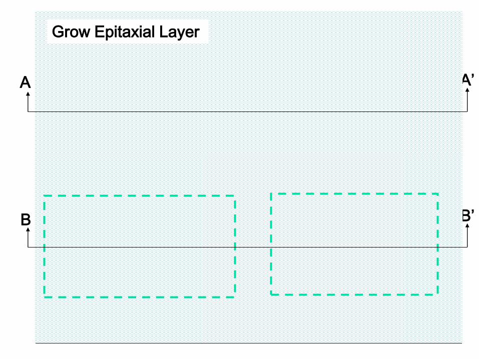
A A’
B’B
p-substrate
n+ buried collector n+ buried collector
Grow Epitaxial Layer

A A’
B’B
Isolation Diffusion
Mask Numbering and Mappings
n+ buried collector
isolation diffusion (p+)
p-base diffusion
n+ emitter
contact
metal
passivation opening
Notes:
• passivation opening for contacts not shown
• isolation diffusion intentionally not shown to scale
Mask 1
Mask 2
Mask 3
Mask 4
Mask 5
Mask 6
Mask 7
A
B
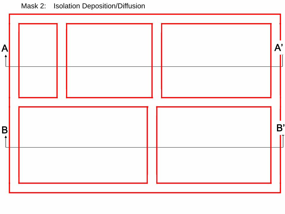
Mask 2: Isolation Deposition/Diffusion
B’
A’

A-A’ Section
B-B’ Section
Isolation Deposition/Diffusion

A A’
B’B
p-substrate
n+ buried collector n+ buried collector
Isolation Diffusion
A A’
B B’
Have created 5 “islands” of n- material on top of p-- substrate
A A’
B’B
p-base diffusion

Mask Numbering and Mappings
n+ buried collector
isolation diffusion (p+)
p-base diffusion
n+ emitter
contact
metal
passivation opening
Notes:
• passivation opening for contacts not shown
• isolation diffusion intentionally not shown to scale
Mask 1
Mask 2
Mask 3
Mask 4
Mask 5
Mask 6
Mask 7

A A’
B’B
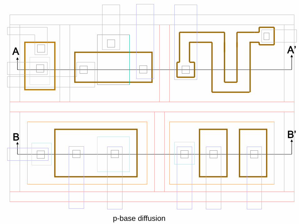
Mask 3: p-base diffusion
A-A’ Section
B-B’ Section
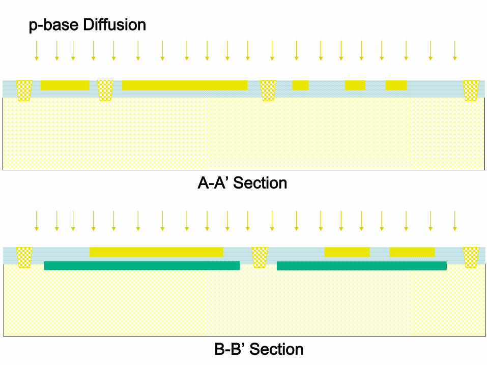
p-base Diffusion

A A’
B’B
p-substrate
n+ buried collector n+ buried collector
p-base Diffusion
A A’
B B’
A A’
B’B
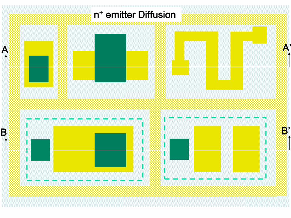
n+ emitter diffusion

Mask Numbering and Mappings
n+ buried collector
isolation diffusion (p+)
p-base diffusion
n+ emitter
contact
metal
passivation opening
Notes:
• passivation opening for contacts not shown
• isolation diffusion intentionally not shown to scale
Mask 1
Mask 2
Mask 3
Mask 4
Mask 5
Mask 6
Mask 7
A A’
B’B
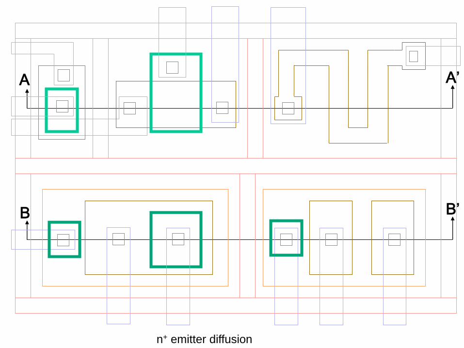
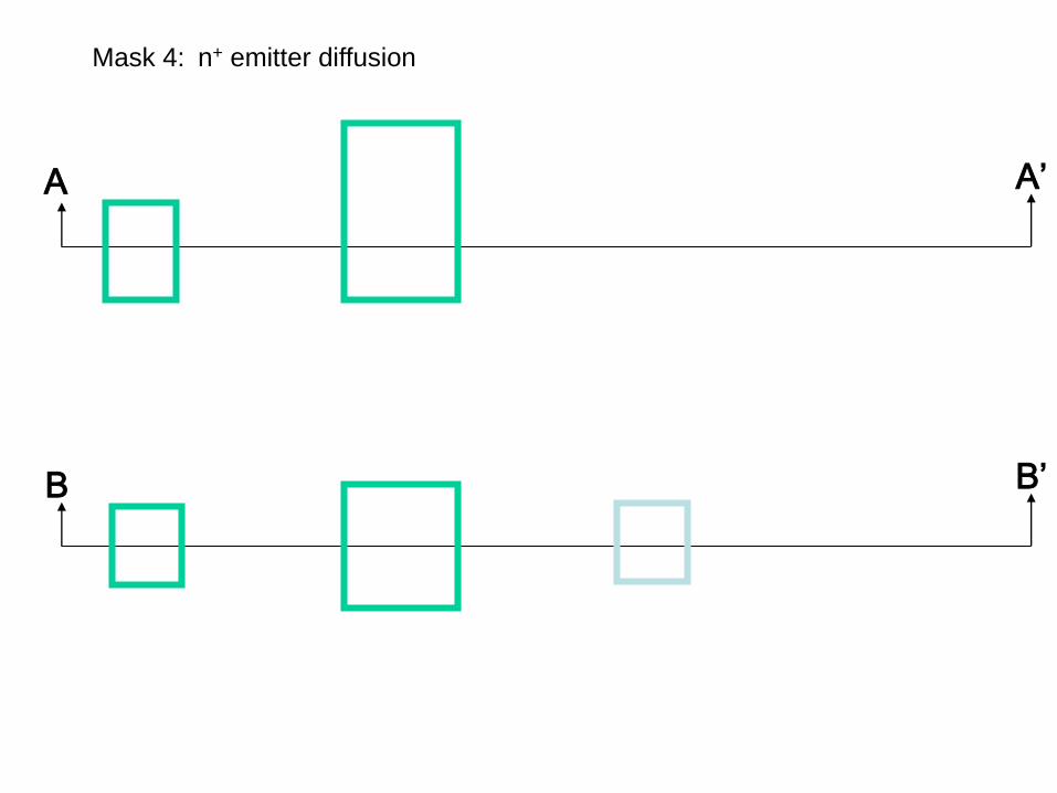
Mask 4: n+ emitter diffusion

A-A’ Section
B-B’ Section
n+ emitter Diffusion
A A’
B’B
p-substrate
n+ buried collector n+ buried collector
A A’
B B’
n+ emitter Diffusion
A-A’ Section
B-B’ Section
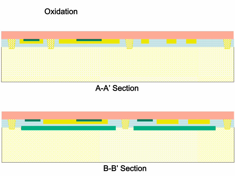
Oxidation
A
B’B
p-substrate
n+ buried collector n+ buried collector
A
B
A’
B’
Oxidation
A A’
B’B
contacts
Mask Numbering and Mappings
n+ buried collector
isolation diffusion (p+)
p-base diffusion
n+ emitter
contact
metal
passivation opening
Notes:
• passivation opening for contacts not shown
• isolation diffusion intentionally not shown to scale
Mask 1
Mask 2
Mask 3
Mask 4
Mask 5
Mask 6
Mask 7
A A’
B’B
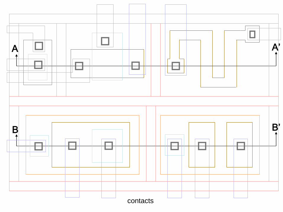
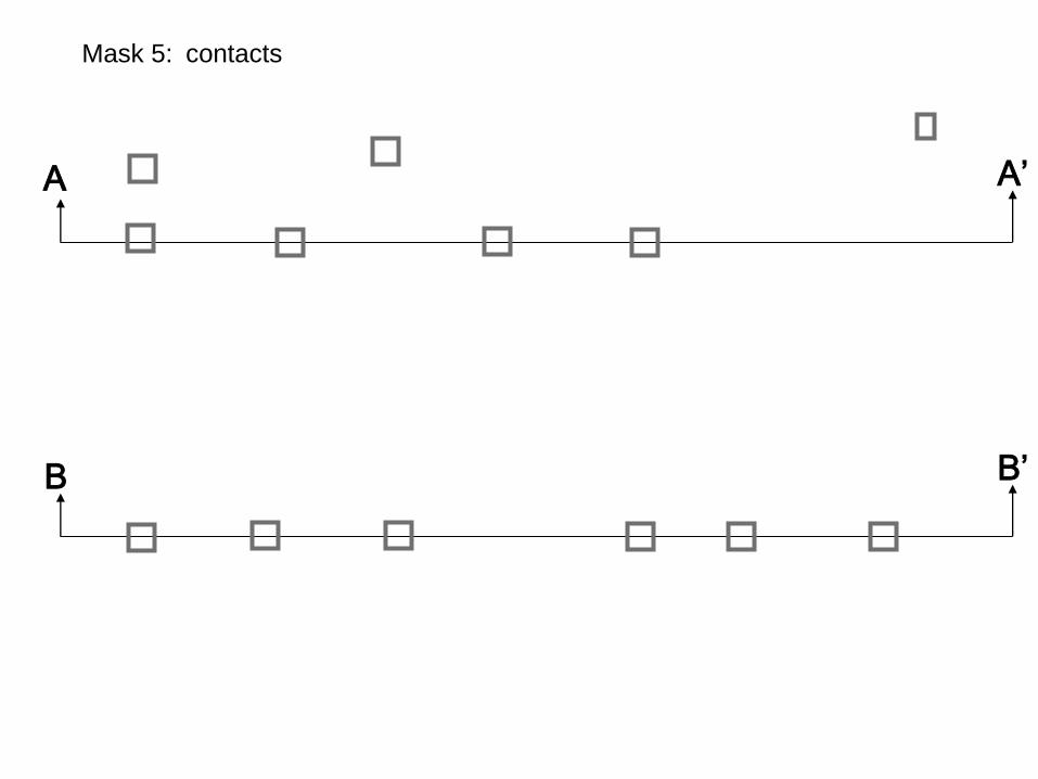
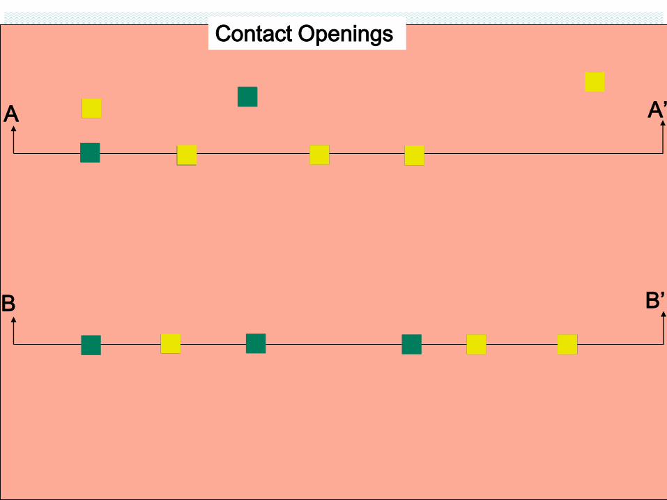
Mask 5: contacts
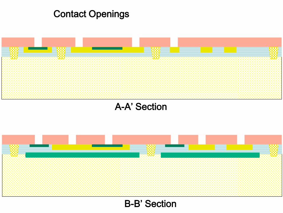
A-A’ Section
B-B’ Section
Contact Openings
A A’
B’B
p-substrate
n+ buried collector n+ buried collector
A
B B’
Contact Openings
A’
A A’
B’B
metal

Mask Numbering and Mappings
n+ buried collector
isolation diffusion (p+)
p-base diffusion
n+ emitter
contact
metal
passivation opening
Notes:
• passivation opening for contacts not shown
• isolation diffusion intentionally not shown to scale
Mask 1
Mask 2
Mask 3
Mask 4
Mask 5
Mask 6
Mask 7

A A’
B’B
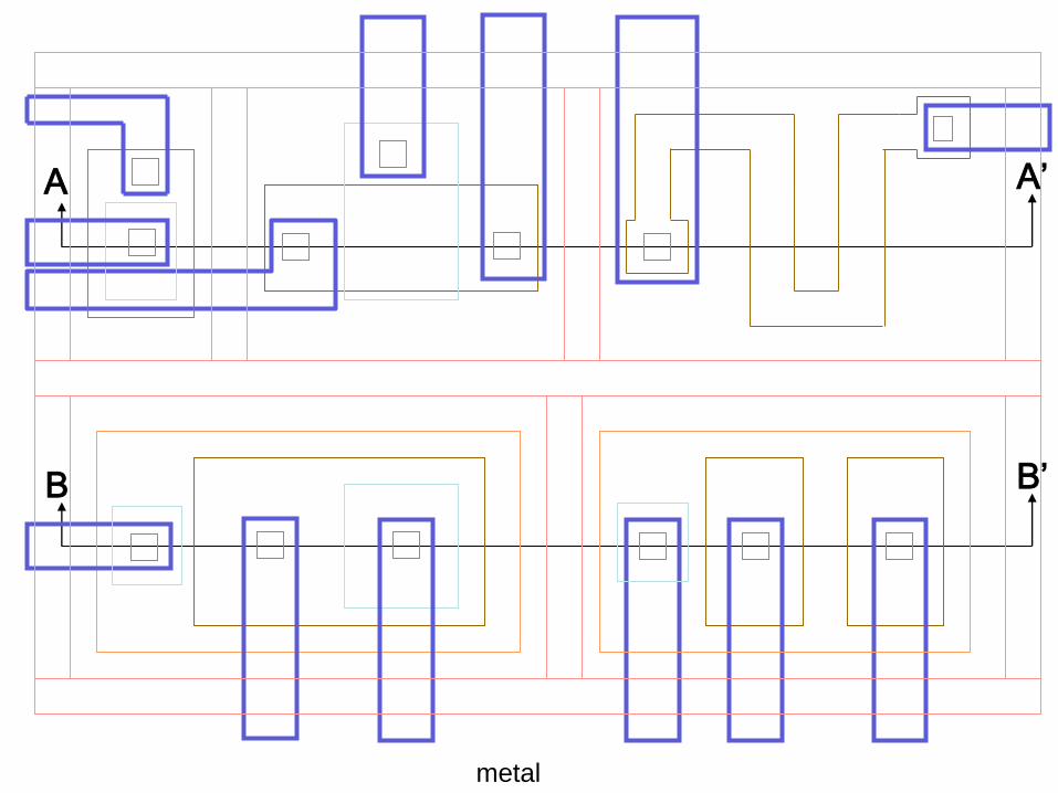
Mask 6: metal
A-A’ Section
B-B’ Section
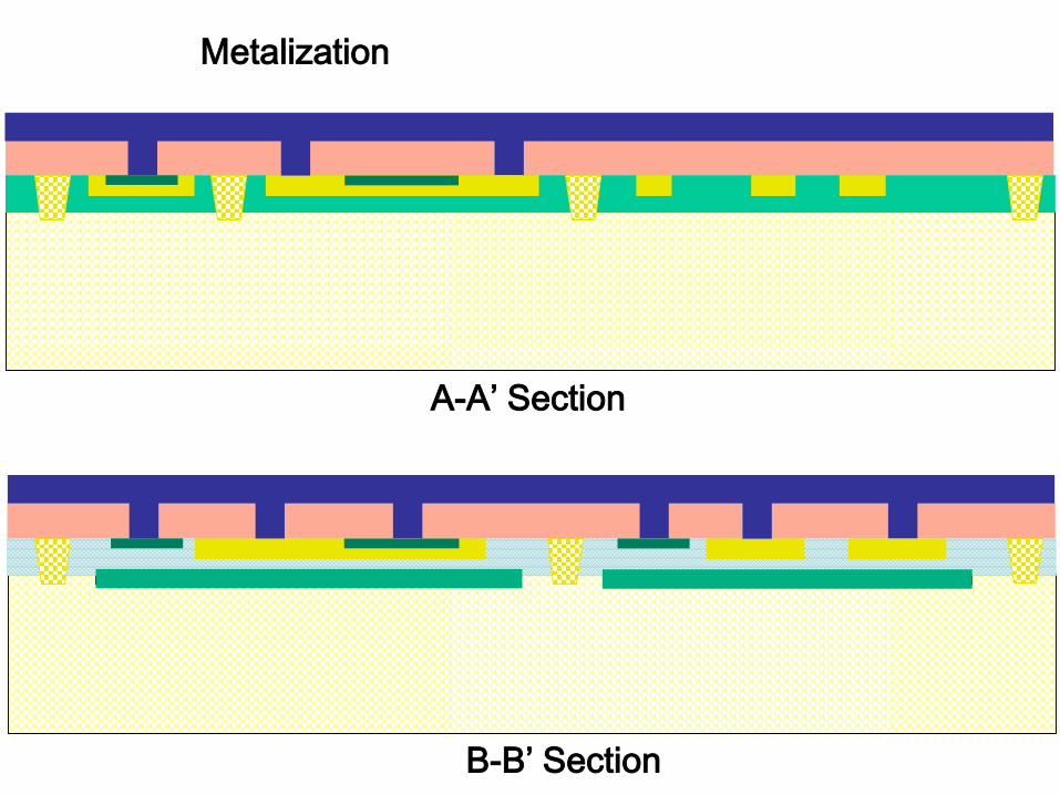
Metalization
A-A’ Section
B-B’ Section
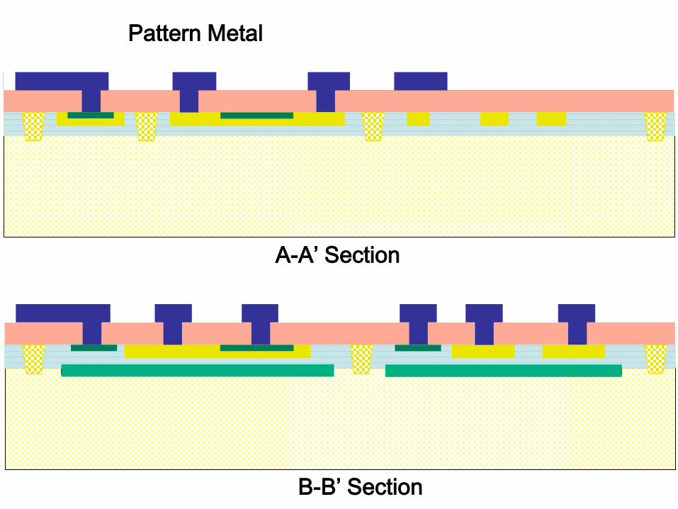
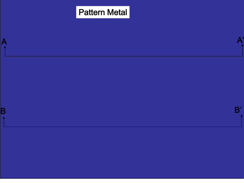
Pattern Metal

A A’
B’B
p-substrate
n+ buried collector n+ buried collector
A
B B’
A’
Metalization
A A’
B’B
A A’
B’B
p-substrate
n+ buried collector n+ buried collector
Pattern Metal
B’B
A A’
A-A’ Section
B-B’ Section
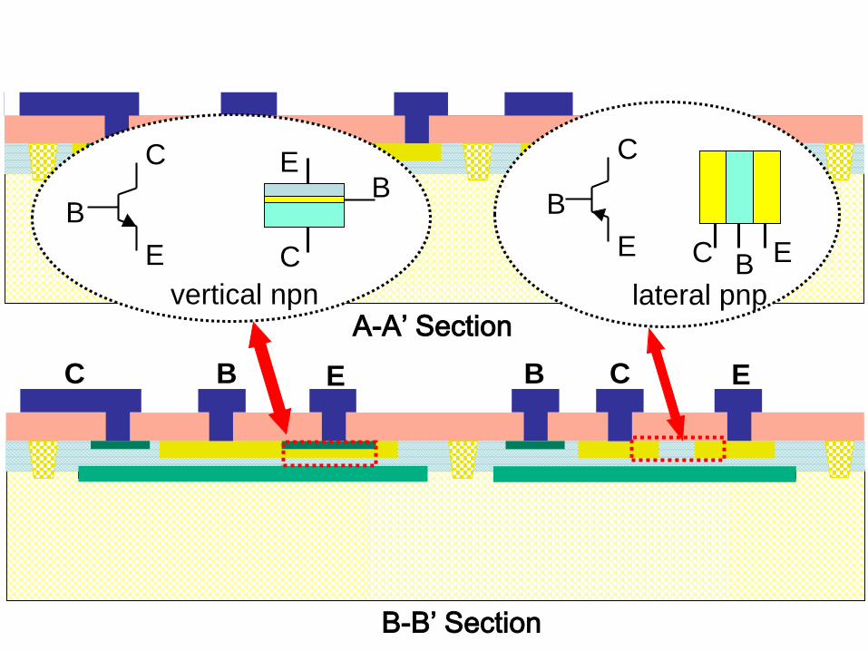
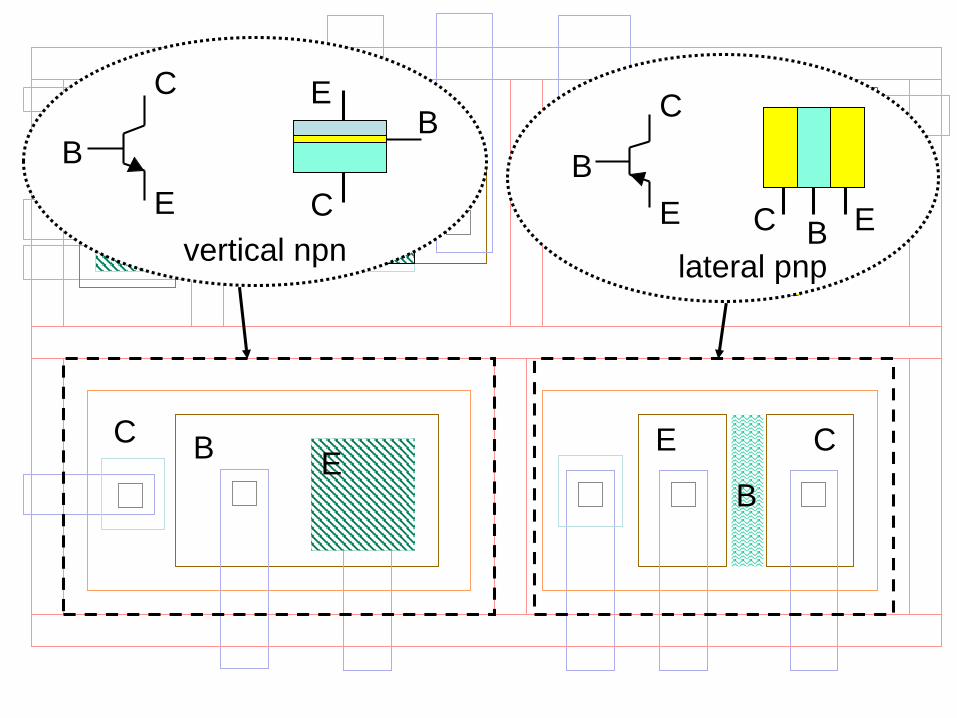
E
C
B
vertical npn
B
C
E
E
B
C
EC Blateral pnp
C B E B C E
A-A’ Section
B-B’ Section
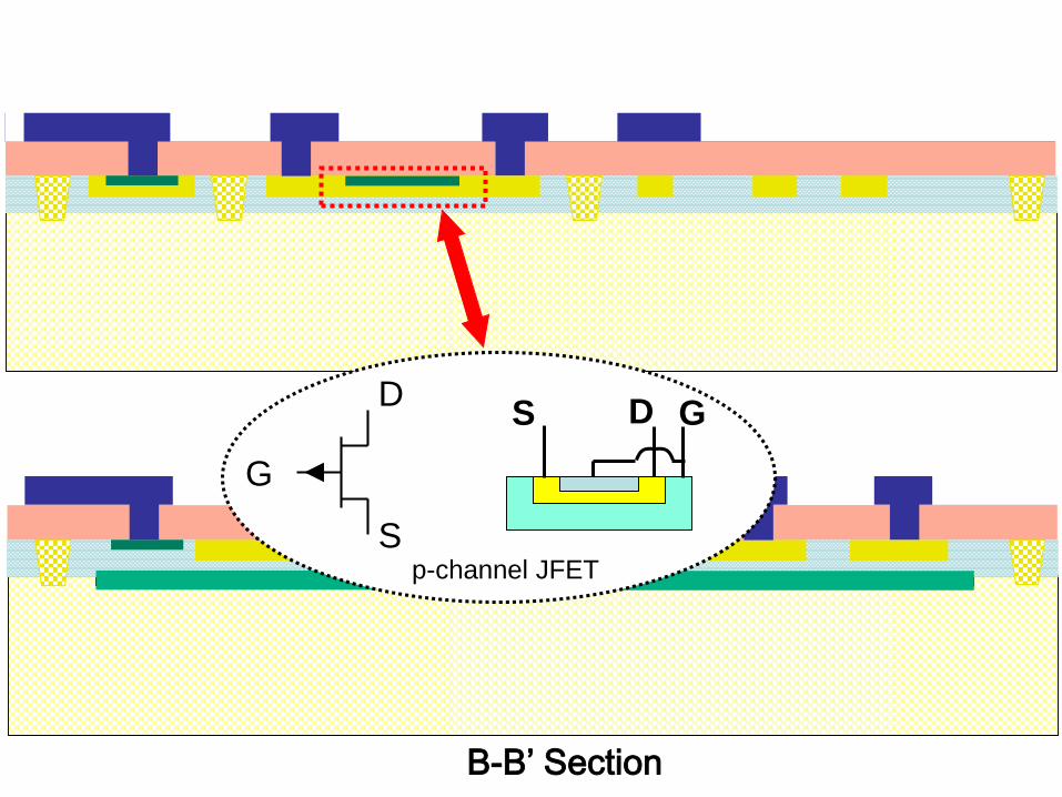
GDS
S
D
G
p-channel JFET
BE
C
E
B
C
EC Blateral pnp
E
C
B
vertical npn
B
C
E
E C
B
L
G
DS
W
Resistor
Diode (capacitor)
GDS
S
D
G
n-channel JFET

Mask Numbering and Mappings
n+ buried collector
isolation diffusion (p+)
p-base diffusion
n+ emitter
contact
metal
passivation opening
Notes:
• passivation opening for contacts not shown
• isolation diffusion intentionally not shown to scale
Mask 1
Mask 2
Mask 3
Mask 4
Mask 5
Mask 6
Mask 7
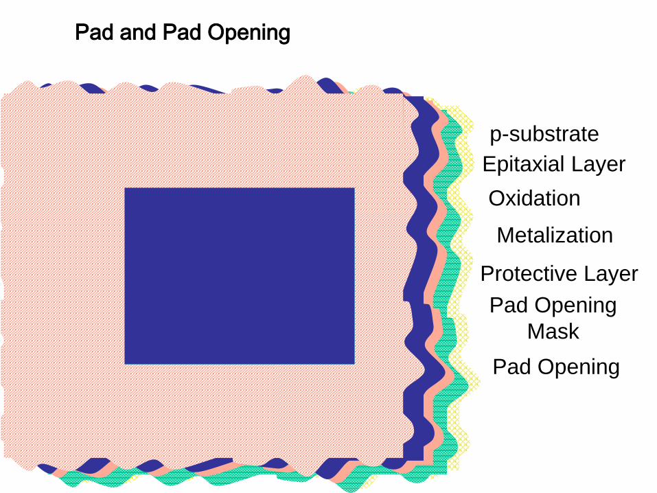
Pad and Pad Opening
Epitaxial Layer
Oxidation
Metalization
Protective Layer
Pad Opening
Pad Opening
Mask
p-substrate

The vertical npn transistor
• Emitter area only geometric parameter that appears in basic device model
• Transistor much larger than emitter
• Multiple-emitter devices often used (TTL Logic) and don’t significantly
increase area
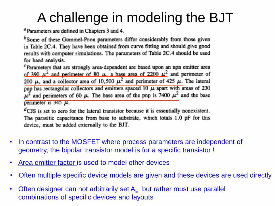
• In contrast to the MOSFET where process parameters are independent of
geometry, the bipolar transistor model is for a specific transistor !
• Area emitter factor is used to model other devices
• Often multiple specific device models are given and these devices are used directly
• Often designer can not arbitrarily set AE but rather must use parallel
combinations of specific devices and layouts
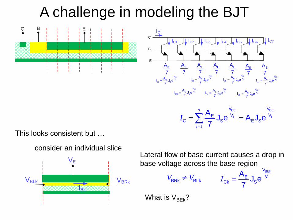
A challenge in modeling the BJT

C B E
Top View of Vertical npn
Cross-Sectional View
A challenge in modeling the BJT

A challenge in modeling the BJT
C B E
C B E
B
E
C
EA
7
EA
7EA
7EA
7EA
7EA
7
EA
7BE
t
V
VEC1 S
AI J e
7
BE
t
V
VEC2 S
AI J e
7
BE
t
V
VEC3 S
AI J e
7
BE
t
V
VEC4 S
AI J e
7
BE
t
V
VEC5 S
AI J e
7
BE
t
V
VEC6 S
AI J e
7
BE
t
V
VEC7 S
AI J e
7
IC
IC1 IC2 IC3 IC4 IC5 IC6 IC7
B
E
C
AE
ICBE
t
V
V
C E SA J eI
7
1
BE BE
t t
V V
V VEC S E S
AJ e A J e
7i
I
This looks consistent but …
A challenge in modeling the BJTC B E
B
E
C
EA
7
EA
7EA
7EA
7EA
7EA
7
EA
7BE
t
V
VEC1 S
AI J e
7
BE
t
V
VEC2 S
AI J e
7
BE
t
V
VEC3 S
AI J e
7
BE
t
V
VEC4 S
AI J e
7
BE
t
V
VEC5 S
AI J e
7
BE
t
V
VEC6 S
AI J e
7
BE
t
V
VEC7 S
AI J e
7
IC
IC1 IC2 IC3 IC4 IC5 IC6 IC7
7
1
BE BE
t t
V V
V VEC S E S
AJ e A J e
7i
I
This looks consistent but …
VBRk
IBk
VBLk
VE
consider an individual sliceLateral flow of base current causes a drop in
base voltage across the base region
BRk BLkV VBEk
t
V
VECk S
AJ e
7I
What is VBEk?

A challenge in modeling the BJT
B
E
C
EA
7
EA
7EA
7EA
7EA
7EA
7
EA
7BE
t
V
VEC1 S
AI J e
7
BE
t
V
VEC2 S
AI J e
7
BE
t
V
VEC3 S
AI J e
7
BE
t
V
VEC4 S
AI J e
7
BE
t
V
VEC5 S
AI J e
7
BE
t
V
VEC6 S
AI J e
7
BE
t
V
VEC7 S
AI J e
7
IC
IC1 IC2 IC3 IC4 IC5 IC6 IC7
7
1
BE BE
t t
V V
V VEC S E S
AJ e A J e
7i
I
This looks consistent but …
VBRk
IBk
VBLk
VE
• Lateral flow of base current causes a drop in base
voltage across the base region
• And that drop differs from one slice to the next
• So VBE is not fixed across the slices
• Since current is exponentially related to VBE, affects
can be significant
• Termed base spreading resistance problem
• Strongly dependent upon layout and contact
placement
• No good models to include this effect
• Major reason designer does not have control of
transistor layout detail in some bipolar processes
• Similar issue does not exist in MOSFET because the
corresponding gate voltage does not change with
position since IG=0

End of Lecture 19