EE 330 Lecture 17 - Iowa State University
49
EE 330 Lecture 17 MOSFET Modeling
Transcript of EE 330 Lecture 17 - Iowa State University
EE 330
Lecture 17
MOSFET Modeling
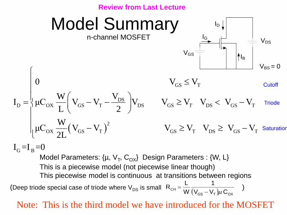
Model SummaryVDS
VBS = 0
VGS
ID
IG
IB
GS T
DSD OX GS T DS GS DS GS T
2
OX GS T GS T DS GS T
G B
0 V V
VWI μC V V V V V V V V
L 2
WμC V V V V V V V
2L
I =I =0
T
Note: This is the third model we have introduced for the MOSFET
Cutoff
Triode
Saturation
OXTGS
CHCVV
1
W
LR
(Deep triode special case of triode where VDS is small )
This is a piecewise model (not piecewise linear though)
This piecewise model is continuous at transitions between regions
n-channel MOSFET
Model Parameters: {µ, VT, COX} Design Parameters : {W, L}
Review from Last Lecture
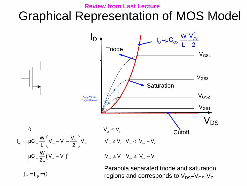
Graphical Representation of MOS Model
G BI =I =0
0
0.5
1
1.5
2
2.5
3
0 1 2 3 4 5
VDS
Cutoff
Triode
Saturation
ID
VDS
VGS1
VGS2
VGS3
VGS4
Deep Triode
RegionRegion
2
DSD OX
VWI =μC
L 2
Parabola separated triode and saturation
regions and corresponds to VDS=VGS-VT
GS T
DS
D OX GS T DS GS DS GS T
2
OX GS T GS T DS GS T
0 V V
VWI μC V V V V V V V V
L 2
WμC V V V V V V V
2L
T
Review from Last Lecture
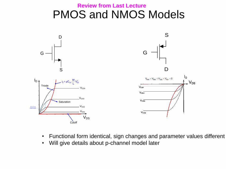
PMOS and NMOS Models
S
D
G
0
0.5
1
1.5
2
2.5
3
0 1 2 3 4 5
VDS
Cutoff
Triode
Saturation
ID
VDS
2
D OX DS
WI = μC V
L
VGS1
VGS2
VGS3
VGS4
Deep Triode
RegionRegion
D
S
G
• Functional form identical, sign changes and parameter values different
• Will give details about p-channel model later
Review from Last Lecture
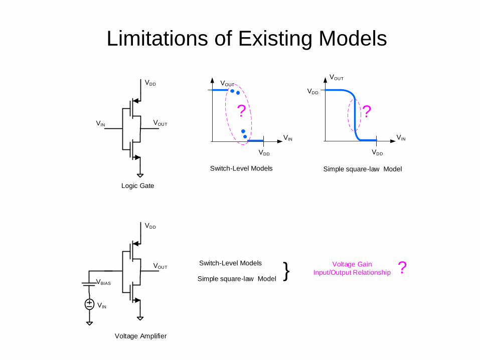
VDD
VIN VOUT
VIN
VDD
VDD
VOUT
VIN
VDD
VOUT
? ?
Switch-Level Models Simple square-law Model
VDD
VIN
VOUT
VBIAS
Logic Gate
Voltage Amplifier
Switch-Level Models
Simple square-law Model?Voltage Gain
Input/Output Relationship}
Limitations of Existing Models
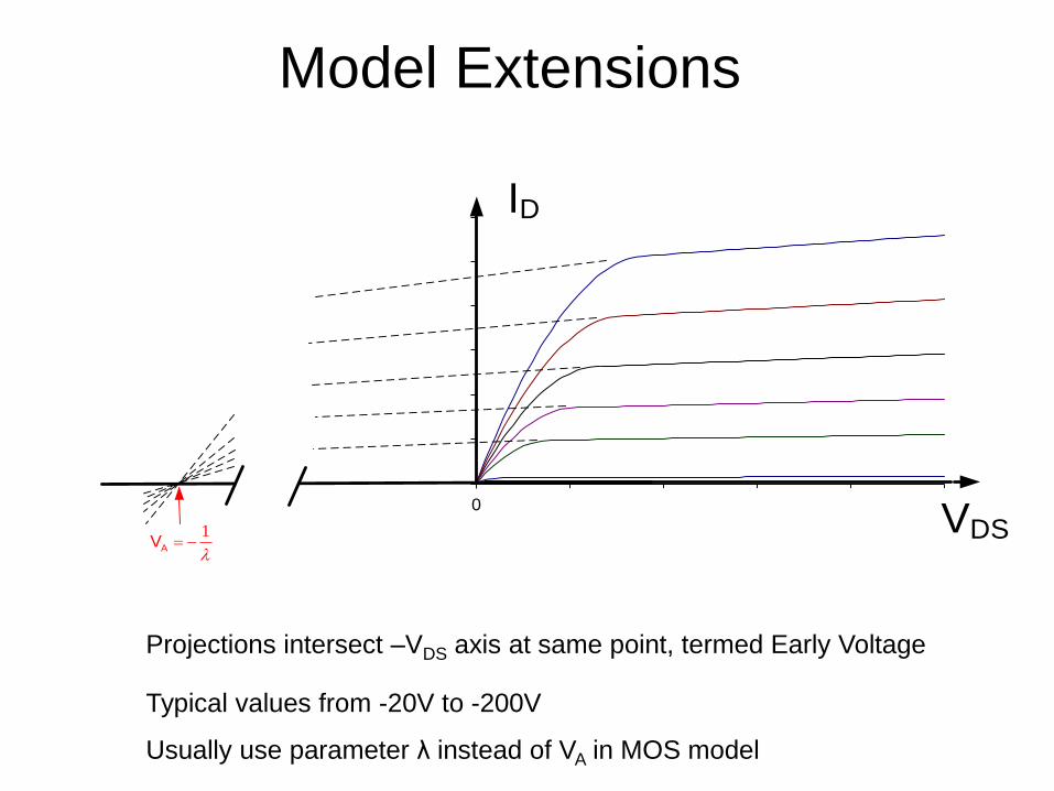
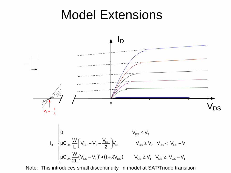
Model Extensions
0
50
100
150
200
250
300
0 1 2 3 4 5
1AV
VDS
ID
Projections intersect –VDS axis at same point, termed Early Voltage
Typical values from -20V to -200V
Usually use parameter λ instead of VA in MOS model
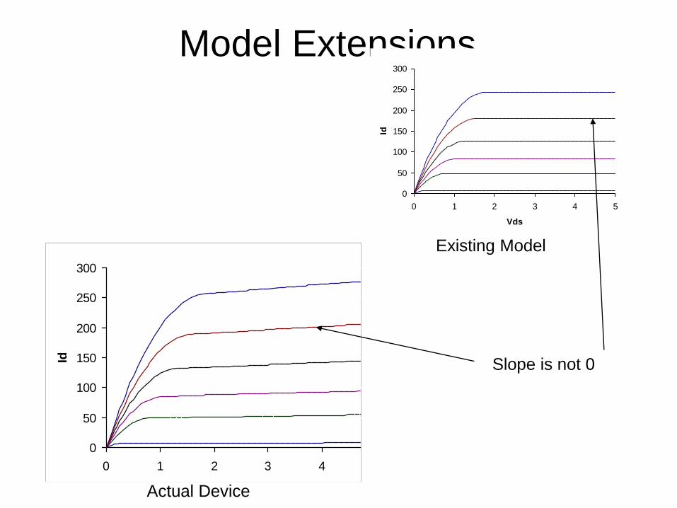
Model Extensions
0
50
100
150
200
250
300
0 1 2 3 4 5
Vds
Id
0
50
100
150
200
250
300
0 1 2 3 4 5
Vds
Id
Existing Model
Actual Device
Slope is not 0
Model Extensions
TGSDSTGSDS
2
TGSOX
TGSDSGSDSDS
TGSOX
TGS
D
VVVVVVVV2L
WμC
VVVVVV2
VVV
L
WμC
VV0
I
1
T
Note: This introduces small discontinuity in model at SAT/Triode transition
0
50
100
150
200
250
300
0 1 2 3 4 5
1AV
VDS
ID
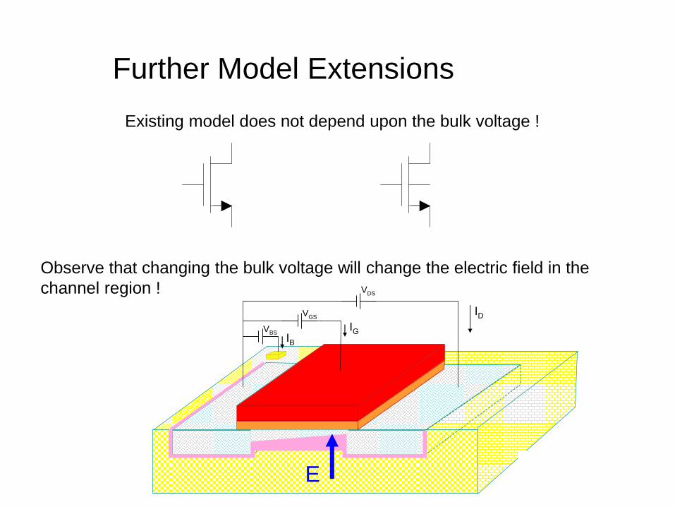
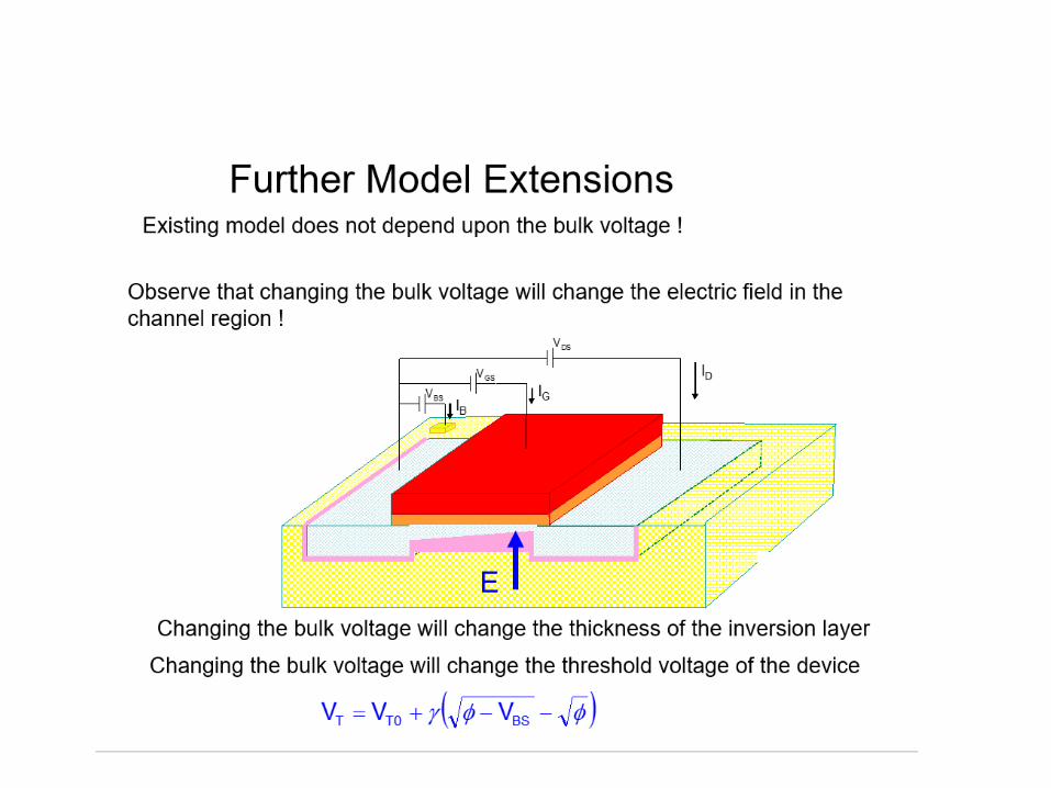
Further Model Extensions
Existing model does not depend upon the bulk voltage !
Observe that changing the bulk voltage will change the electric field in the
channel region !
VBS
VGS
VDS
IDIG
IB
(VBS small)
E
-6 -5 -4 -3 -2 -1 0 1
VTH
-5V
VTH0
VBS
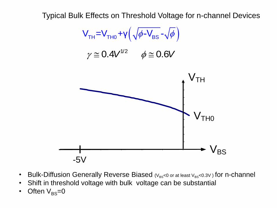
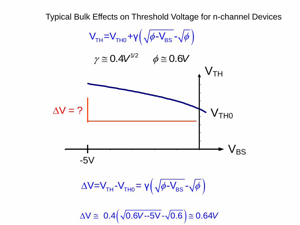
TH TH0 BSV =V +γ -V -
Typical Bulk Effects on Threshold Voltage for n-channel Devices
• Bulk-Diffusion Generally Reverse Biased (VBS<0 or at least VBS<0.3V ) for n-channel
• Shift in threshold voltage with bulk voltage can be substantial
• Often VBS=0
1/20.4 0.6V V
-6 -5 -4 -3 -2 -1 0 1
VTH
-5V
VTH0
VBS
TH TH0 BSV =V +γ -V -
Typical Bulk Effects on Threshold Voltage for n-channel Devices
1/20.4 0.6V V
V = ?
TH TH0 BSV=V -V = γ -V -
V 0.4 0.6 --5V- 0.6 0.64V V
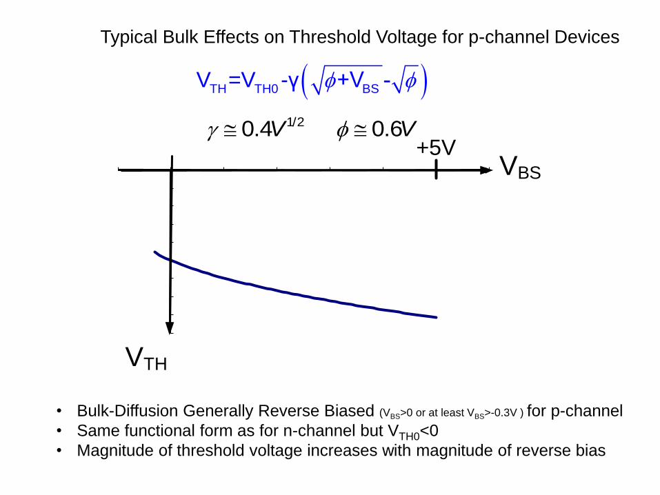
TH TH0 BSV =V -γ +V -
Typical Bulk Effects on Threshold Voltage for p-channel Devices
• Bulk-Diffusion Generally Reverse Biased (VBS>0 or at least VBS>-0.3V ) for p-channel
• Same functional form as for n-channel but VTH0<0
• Magnitude of threshold voltage increases with magnitude of reverse bias
1/20.4 0.6V V
VTH
VBS
+5V
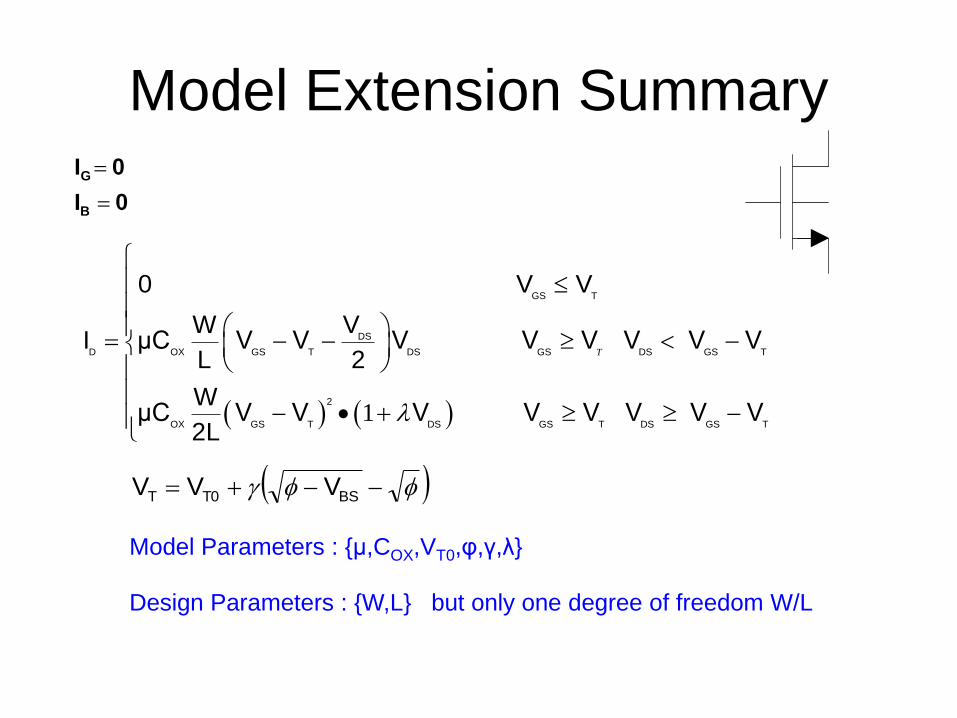
Model Extension Summary
1
GS T
DS
D OX GS T DS GS DS GS T
2
OX GS T DS GS T DS GS T
0 V V
VWI μC V V V V V V V V
L 2
WμC V V V V V V V V
2L
T
BST0T VVV
Model Parameters : {μ,COX,VT0,φ,γ,λ}
Design Parameters : {W,L} but only one degree of freedom W/L
0I
0I
B
G
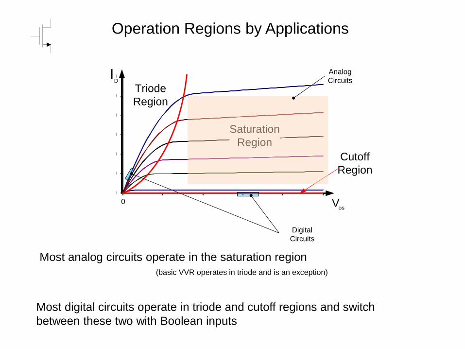
Operation Regions by Applications
0
50
100
150
200
250
300
0 1 2 3 4 5
Id
Vds
Saturation
Region
Triode
Region
Cutoff
Region
Analog
Circuits
Digital
Circuits
DI
DSV
Most analog circuits operate in the saturation region
(basic VVR operates in triode and is an exception)
Most digital circuits operate in triode and cutoff regions and switch
between these two with Boolean inputs
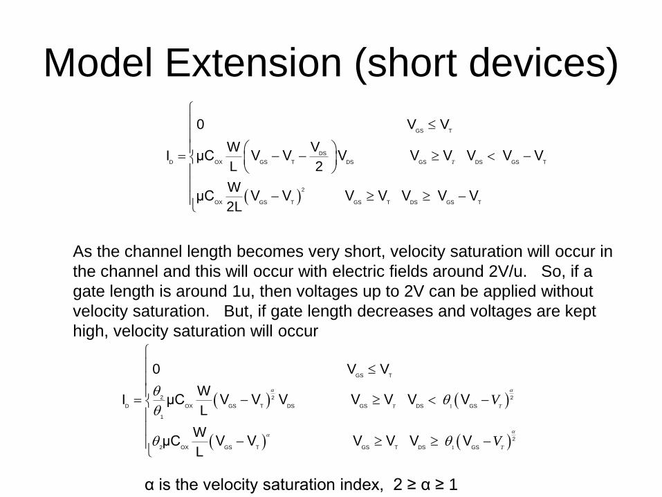
Model Extension (short devices)
GS T
DS
D OX GS T DS GS DS GS T
2
OX GS T GS T DS GS T
0 V V
VWI μC V V V V V V V V
L 2
WμC V V V V V V V
2L
T
As the channel length becomes very short, velocity saturation will occur in
the channel and this will occur with electric fields around 2V/u. So, if a
gate length is around 1u, then voltages up to 2V can be applied without
velocity saturation. But, if gate length decreases and voltages are kept
high, velocity saturation will occur
1
1
GS T
2 2 2
D OX GS T DS GS DS GS
1
2
2 OX GS T GS T DS GS
0 V V
WI μC V V V V V V V
L
WμC V V V V V V
L
T T
T
V
V
α is the velocity saturation index, 2 ≥ α ≥ 1
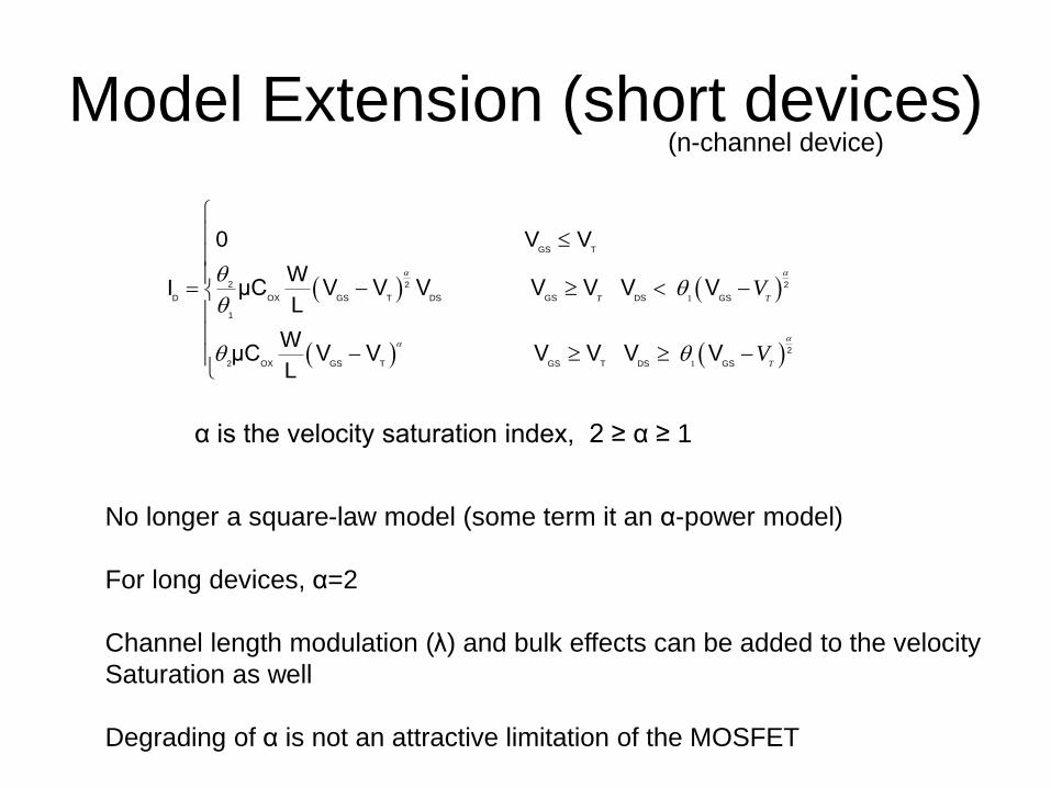
Model Extension (short devices)
1
1
GS T
2 2 2
D OX GS T DS GS DS GS
1
2
2 OX GS T GS T DS GS
0 V V
WI μC V V V V V V V
L
WμC V V V V V V
L
T T
T
V
V
α is the velocity saturation index, 2 ≥ α ≥ 1
No longer a square-law model (some term it an α-power model)
For long devices, α=2
Channel length modulation (λ) and bulk effects can be added to the velocity
Saturation as well
Degrading of α is not an attractive limitation of the MOSFET
(n-channel device)
Model Extension (BSIM model)
ID
VDS
VGS1
VGS2
VGS3
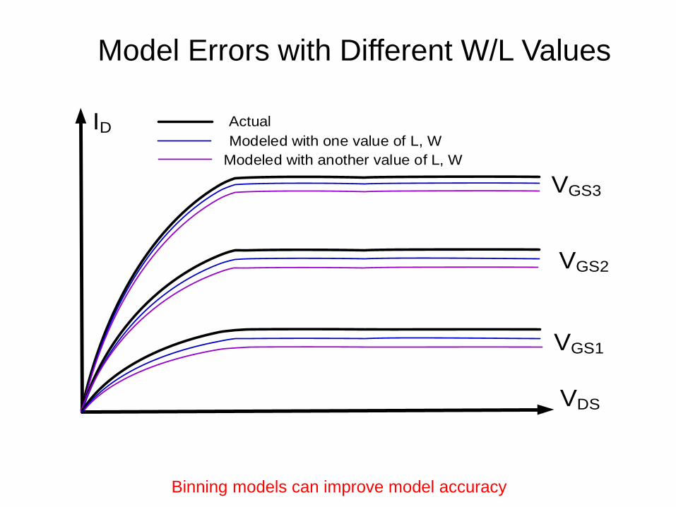
Actual
Modeled with one value of L, W
Modeled with another value of L, W
Model Errors with Different W/L Values
Binning models can improve model accuracy
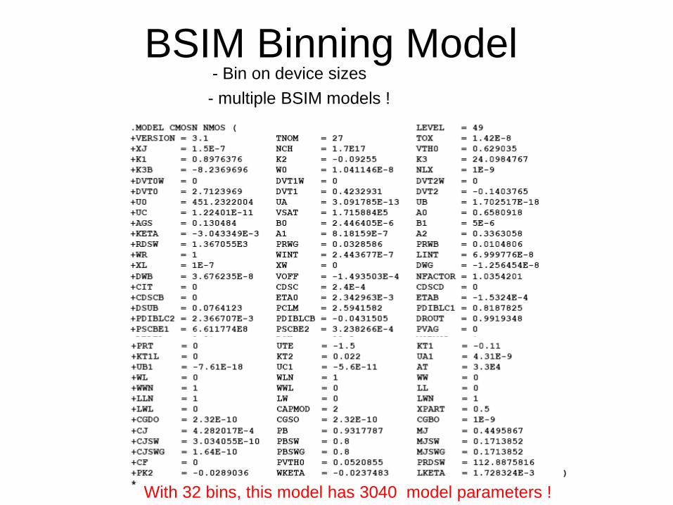
BSIM Binning Model - multiple BSIM models !
With 32 bins, this model has 3040 model parameters !
- Bin on device sizes
ID
VGS1
VGS2
VGS3
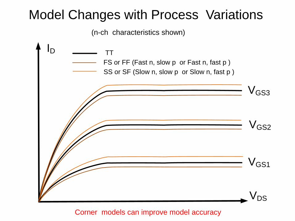
TT
FS or FF (Fast n, slow p or Fast n, fast p )
SS or SF (Slow n, slow p or Slow n, fast p )
VDS
Model Changes with Process Variations
(n-ch characteristics shown)
Corner models can improve model accuracy
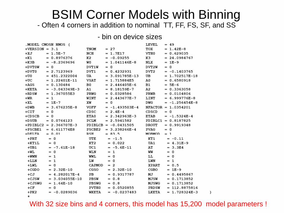
BSIM Corner Models with Binning
- bin on device sizes
With 32 size bins and 4 corners, this model has 15,200 model parameters !
- Often 4 corners in addition to nominal TT, FF, FS, SF, and SS
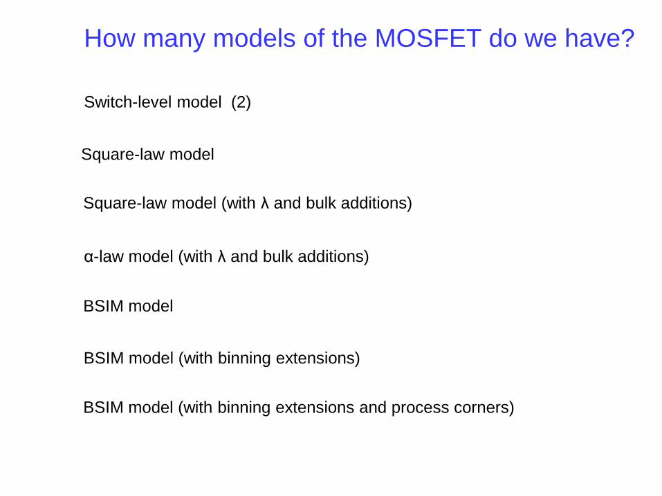
How many models of the MOSFET do we have?
Switch-level model (2)
Square-law model (with λ and bulk additions)
α-law model (with λ and bulk additions)
BSIM model
Square-law model
BSIM model (with binning extensions)
BSIM model (with binning extensions and process corners)
ID
VDS
VGS1
VGS2
VGS3
Actual
Modeled with one model
Local Agreement
with Any Model
(and W/L variations or
Process Variations)
(and W/L variations or
Process Variations)
(and W/L variations or
Process Variations)
(and W/L variations or
Process Variations)
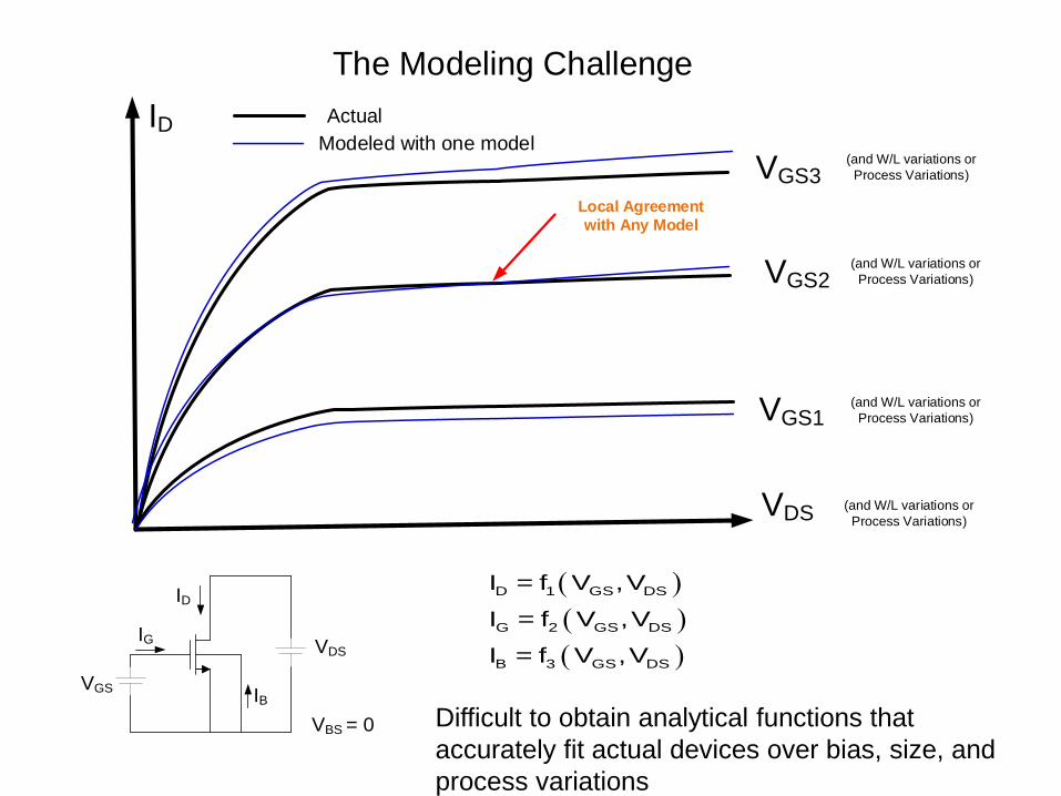
The Modeling Challenge
VDS
VBS = 0
VGS
ID
IG
IB
D 1 GS DS
G 2 GS DS
B 3 GS DS
I = f V ,V
I = f V ,V
I = f V ,V
Difficult to obtain analytical functions that
accurately fit actual devices over bias, size, and
process variations
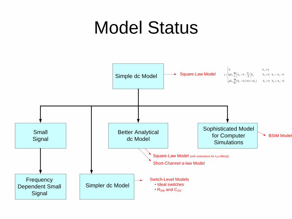
Model Status
Simple dc Model
Small
Signal
Frequency
Dependent Small
Signal
Better Analytical
dc Model
Sophisticated Model
for Computer
Simulations
Simpler dc Model
Square-Law Model
Square-Law Model (with extensions for λ,γ effects)
Short-Channel α-law Model
BSIM Model
Switch-Level Models
• Ideal switches
• RSW and CGS
1
GS T
DS
D OX GS T DS GS DS GS T
2
OX GS T DS GS T DS GS T
0 V V
VWI μC V V V V V V V V
L 2
WμC V V V V V V V V
2L
T
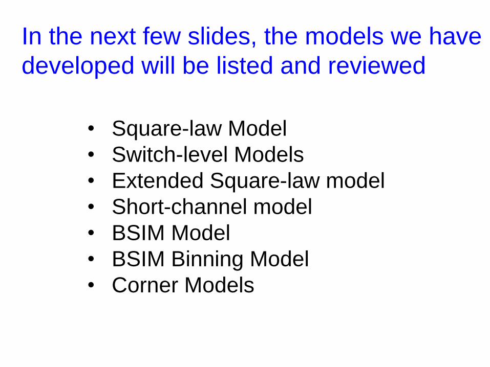
In the next few slides, the models we have
developed will be listed and reviewed
• Square-law Model
• Switch-level Models
• Extended Square-law model
• Short-channel model
• BSIM Model
• BSIM Binning Model
• Corner Models
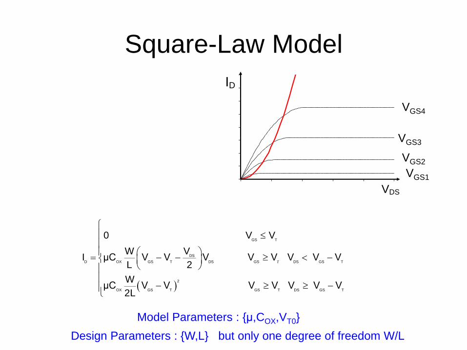
Square-Law Model
ID
VDS
GS T
DS
D OX GS T DS GS DS GS T
2
OX GS T GS T DS GS T
0 V V
VWI μC V V V V V V V V
L 2
WμC V V V V V V V
2L
T
VGS1
VGS3
VGS2
VGS4
Model Parameters : {μ,COX,VT0}
Design Parameters : {W,L} but only one degree of freedom W/L
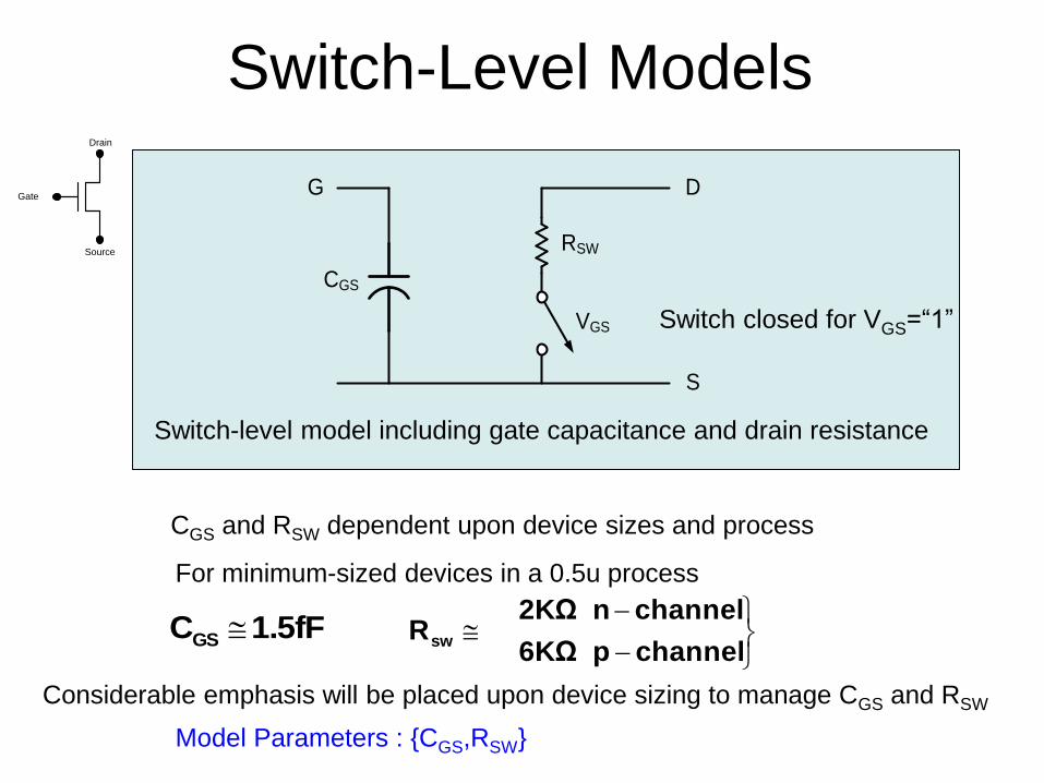
VGS
RSW
CGS
S
DG
Switch-Level Models
Switch-level model including gate capacitance and drain resistance
Switch closed for VGS=“1”
CGS and RSW dependent upon device sizes and process
For minimum-sized devices in a 0.5u process
1.5fFCGS
channelp6KΩ
channeln2KΩRsw
Considerable emphasis will be placed upon device sizing to manage CGS and RSW
Drain
Gate
Source
Model Parameters : {CGS,RSW}
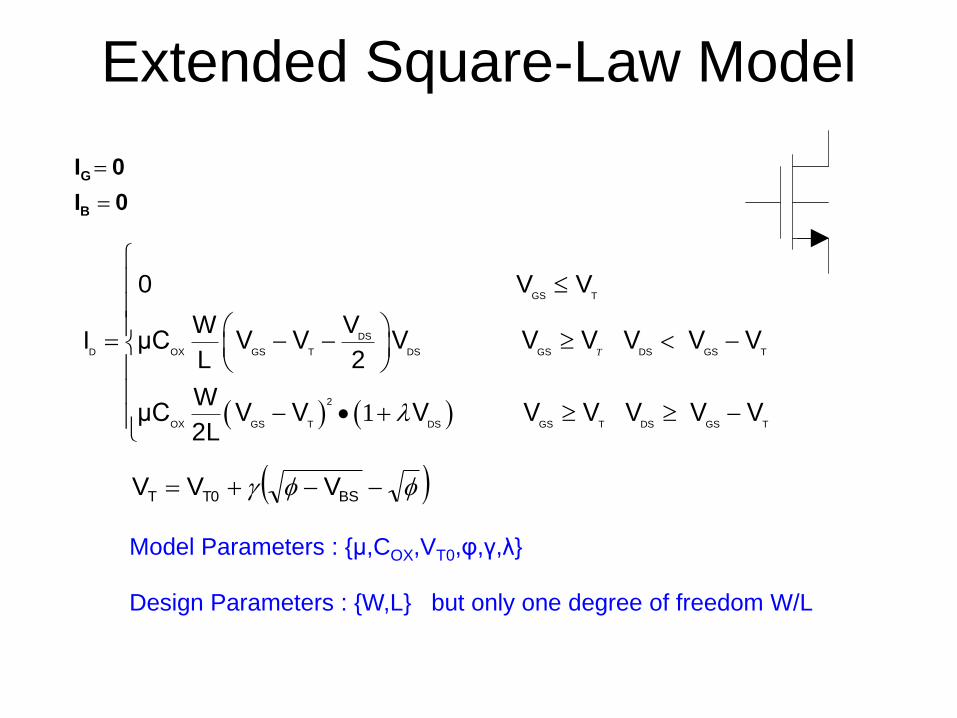
Extended Square-Law Model
1
GS T
DS
D OX GS T DS GS DS GS T
2
OX GS T DS GS T DS GS T
0 V V
VWI μC V V V V V V V V
L 2
WμC V V V V V V V V
2L
T
BST0T VVV
Model Parameters : {μ,COX,VT0,φ,γ,λ}
Design Parameters : {W,L} but only one degree of freedom W/L
0I
0I
B
G
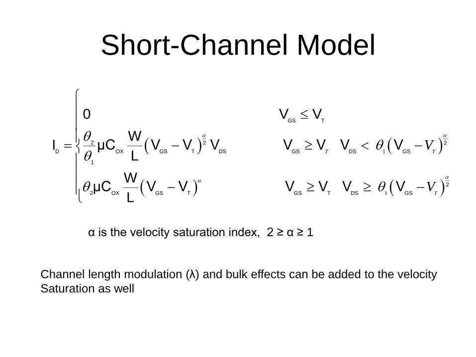
Short-Channel Model
1
1
GS T
2 2 2
D OX GS T DS GS DS GS
1
2
2 OX GS T GS T DS GS
0 V V
WI μC V V V V V V V
L
WμC V V V V V V
L
T T
T
V
V
α is the velocity saturation index, 2 ≥ α ≥ 1
Channel length modulation (λ) and bulk effects can be added to the velocity
Saturation as well
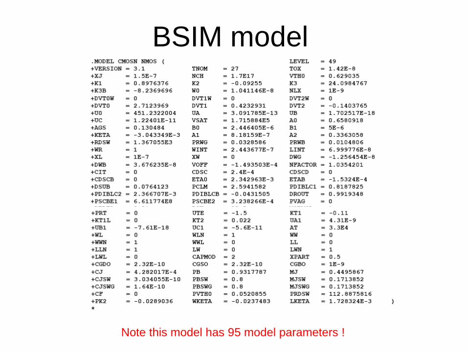
BSIM model
Note this model has 95 model parameters !

BSIM Binning Model - multiple BSIM models !
With 32 bins, this model has 3040 model parameters !
- Bin on device sizes
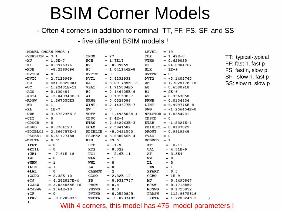
BSIM Corner Models
- five different BSIM models !
With 4 corners, this model has 475 model parameters !
- Often 4 corners in addition to nominal TT, FF, FS, SF, and SS
TT: typical-typical
FF: fast n, fast p
FS: fast n, slow p
SF: slow n, fast p
SS: slow n, slow p
W
L
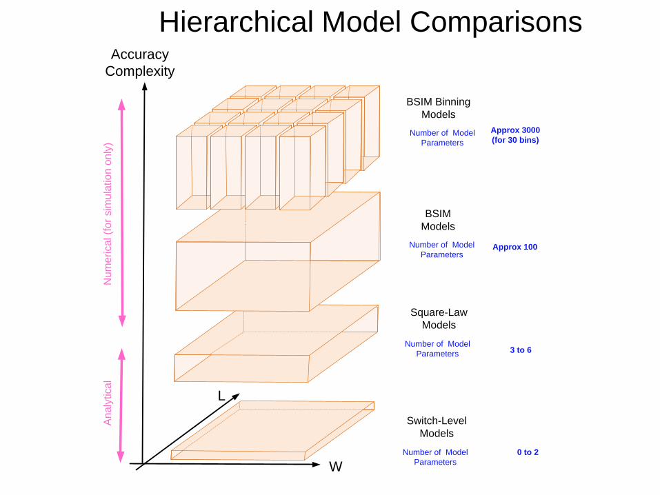
Accuracy
Complexity
Switch-Level
Models
Number of Model
Parameters
0 to 2
Square-Law
Models
Number of Model
Parameters 3 to 6
BSIM
Models
Number of Model
ParametersApprox 100
BSIM Binning
Models
Number of Model
Parameters
Approx 3000
(for 30 bins)
An
aly
tica
lN
um
erica
l (f
or
sim
ula
tio
n o
nly
)
Hierarchical Model Comparisons
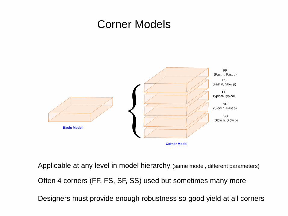
TT
Typical-Typical
SS
(Slow n, Slow p)
SF
(Slow n, Fast p)
FS
(Fast n, Slow p)
FF
(Fast n, Fast p)
Basic Model
Corner Model
Corner Models
Applicable at any level in model hierarchy (same model, different parameters)
Often 4 corners (FF, FS, SF, SS) used but sometimes many more
Designers must provide enough robustness so good yield at all corners
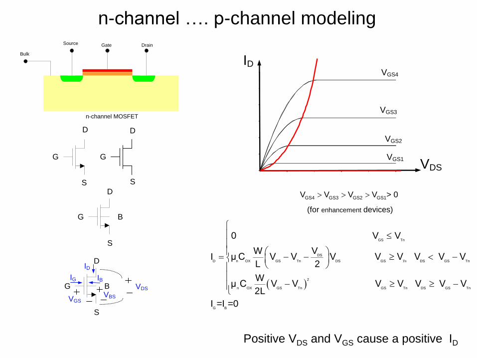
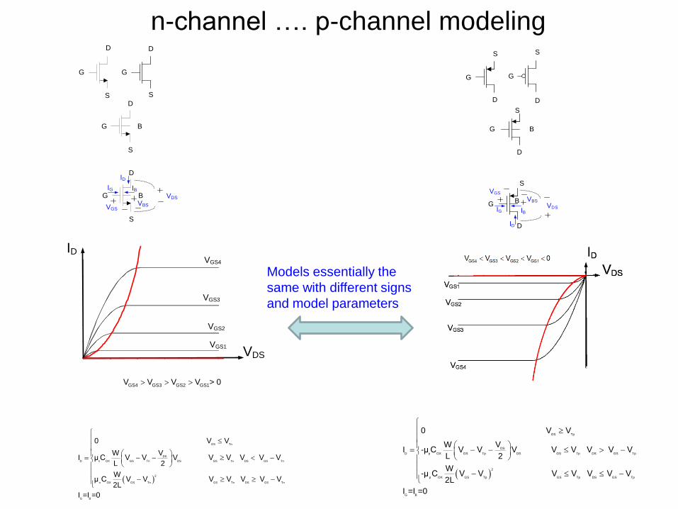
n-channel …. p-channel modeling
GS Tn
DS
D n OX GS Tn DS GS DS GS Tn
2
n OX GS Tn GS Tn DS GS Tn
G B
0 V V
VWI μ C V V V V V V V V
L 2
Wμ C V V V V V V V
2L
I =I =0
Tn
0
0.5
1
1.5
2
2.5
3
0 1 2 3 4 5
VDS
ID
VGS1
VGS2
VGS4
VGS3
GS4 GS3 GS2 GS1V V V V > 0
VDS
D
BG
S
VDS
VGSVBS
ID
IG IB
D D
S S
G G
D
BG
S
Gate DrainSource
Bulk
n-channel MOSFET
Positive VDS and VGS cause a positive ID
(for enhancement devices)
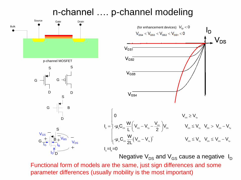
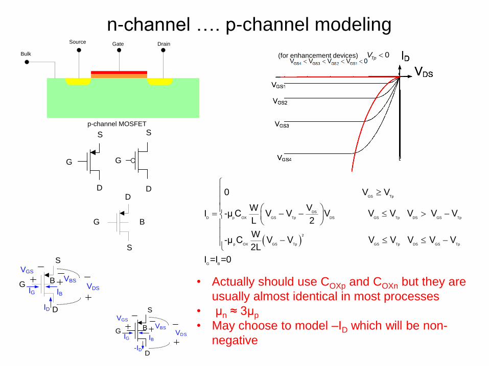
n-channel …. p-channel modeling
D D
S S
G G
D
BG
S
D
BG
S
VDS
VGS
VBS
ID
IG IB
GS Tp
DS
D p OX GS Tp DS GS Tp DS GS Tp
2
p OX GS Tp GS Tp DS GS Tp
G B
0 V V
VWI -μ C V V V V V V V V
L 2
W-μ C V V V V V V V
2L
I =I =0
Gate DrainSource
Bulk
p-channel MOSFET
Negative VDS and VGS cause a negative ID
(for enhancement devices)
Functional form of models are the same, just sign differences and some
parameter differences (usually mobility is the most important)
0TpV
n-channel …. p-channel modeling
D D
S S
G G
D
BG
S
D
BG
S
VDS
VGS
VBS
ID
IG IB
GS Tp
DS
D p OX GS Tp DS GS Tp DS GS Tp
2
p OX GS Tp GS Tp DS GS Tp
G B
0 V V
VWI -μ C V V V V V V V V
L 2
W-μ C V V V V V V V
2L
I =I =0
Gate DrainSource
Bulk
p-channel MOSFET
(for enhancement devices)
• Actually should use COXp and COXn but they are
usually almost identical in most processes
• μn ≈ 3μp
• May choose to model –ID which will be non-
negativeD
BG
S
VDS
VGS
VBS
-ID
IG IB
0TpV
n-channel …. p-channel modeling
D
BG
S
VDS
VGS
VBS
ID
IG IB
GS Tp
DS
D p OX GS Tp DS GS Tp DS GS Tp
2
p OX GS Tp GS Tp DS GS Tp
G B
0 V V
VWI -μ C V V V V V V V V
L 2
W-μ C V V V V V V V
2L
I =I =0
Gate DrainSource
Bulk
p-channel MOSFET
(for enhancement devices)
GS Tp
DS
D p OX GS Tp DS GS Tp DS GS Tp
2
p OX GS Tp GS Tp DS GS Tp
G B
0 V V
VWI μ C V V V V V V V V
L 2
Wμ C V V V V V V V
2L
I =I =0
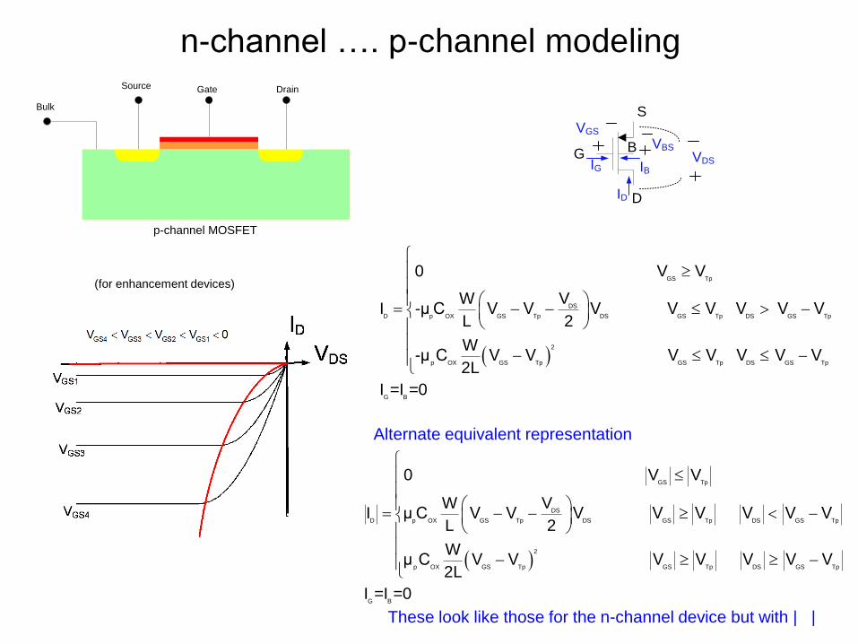
Alternate equivalent representation
These look like those for the n-channel device but with | |
D D
S S
G G
D
BG
S
D
BG
S
VDS
VGSVBS
ID
IG IB
0
0.5
1
1.5
2
2.5
3
0 1 2 3 4 5
VDS
ID
VGS1
VGS2
VGS4
VGS3
GS4 GS3 GS2 GS1V V V V > 0
VDS
GS Tn
DS
D n OX GS Tn DS GS DS GS Tn
2
n OX GS Tn GS Tn DS GS Tn
G B
0 V V
VWI μ C V V V V V V V V
L 2
Wμ C V V V V V V V
2L
I =I =0
Tn
D D
S S
G G
D
BG
S
D
BG
S
VDS
VGS
VBS
ID
IG IB
GS Tp
DS
D p OX GS Tp DS GS Tp DS GS Tp
2
p OX GS Tp GS Tp DS GS Tp
G B
0 V V
VWI -μ C V V V V V V V V
L 2
W-μ C V V V V V V V
2L
I =I =0
n-channel …. p-channel modeling
Models essentially the
same with different signs
and model parameters
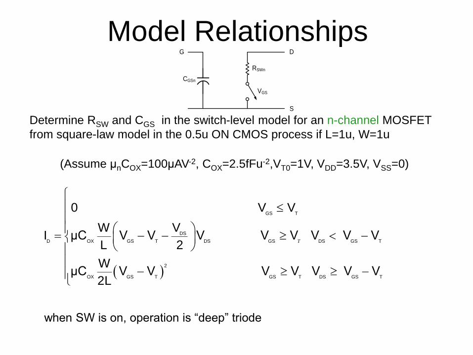
Model Relationships
Determine RSW and CGS in the switch-level model for an n-channel MOSFET
from square-law model in the 0.5u ON CMOS process if L=1u, W=1u
(Assume μnCOX=100μAV-2, COX=2.5fFu-2,VT0=1V, VDD=3.5V, VSS=0)
GS T
DS
D OX GS T DS GS DS GS T
2
OX GS T GS T DS GS T
0 V V
VWI μC V V V V V V V V
L 2
WμC V V V V V V V
2L
T
when SW is on, operation is “deep” triode
VGS
RSWn
CGSn
S
DG
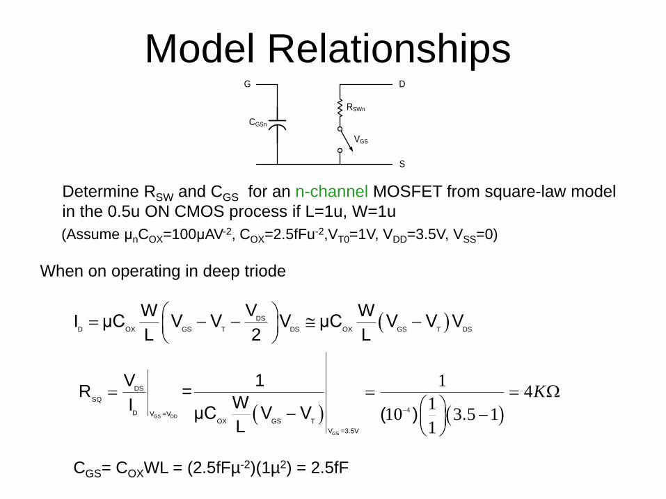
Model Relationships
(Assume μnCOX=100μAV-2, COX=2.5fFu-2,VT0=1V, VDD=3.5V, VSS=0)
DS
D OX GS T DS OX GS T DS
VW WI μC V V V μC V V V
L 2 L
4
14
110 3 5 1
1GS DD
GS
DS
SQ
D V =VOX GS T
V =3.5V
V 1R =
WIμC V V ( ) .
L
K
CGS= COXWL = (2.5fFµ-2)(1µ2) = 2.5fF
Determine RSW and CGS for an n-channel MOSFET from square-law model
in the 0.5u ON CMOS process if L=1u, W=1u
When on operating in deep triode
VGS
RSWn
CGSn
S
DG
Model Relationships
(μpCOX=33μAV-2 , μnCOX=100μAV-2 , COX=2.5fFu-2,VT0=1V, VDD=3.5V, VSS=0)
GS T
DS
D OX GS T DS GS DS GS T
2
OX GS T GS T DS GS T
0 V V
VW-I μC V V V V V V V V
L 2
WμC V V V V V V V
2L
T
When SW is on, operation is “deep” triode
Determine RSW and CGS for an p-channel MOSFET from square-law model
in the 0.5u ON CMOS process if L=1u, W=1u
Observe µn\ µp≈3
VGS
RSWp
CGSp
S
DG
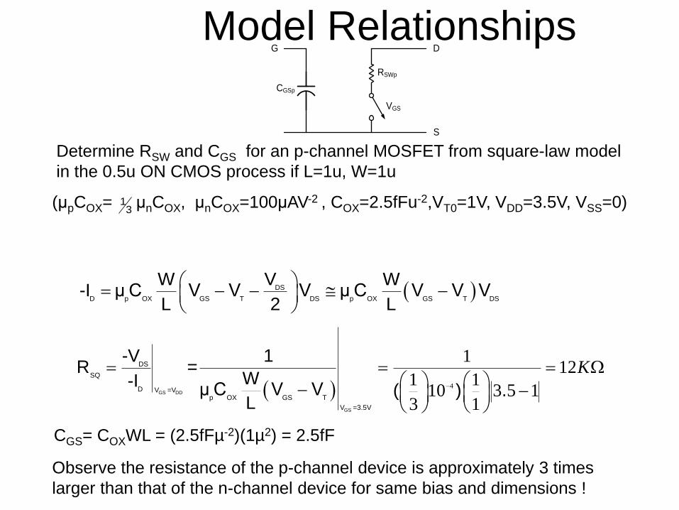
Model Relationships
DS
D p OX GS T DS p OX GS T DS
VW W-I μ C V V V μ C V V V
L 2 L
4
112
1 110 3 5 1
3 1GS DD
GS
DS
SQ
D V =Vp OX GS T
V =3.5V
-V 1R =
W-Iμ C V V ( ) .
L
K
CGS= COXWL = (2.5fFµ-2)(1µ2) = 2.5fF
Determine RSW and CGS for an p-channel MOSFET from square-law model
in the 0.5u ON CMOS process if L=1u, W=1u
(μpCOX= μnCOX, μnCOX=100μAV-2 , COX=2.5fFu-2,VT0=1V, VDD=3.5V, VSS=0)
Observe the resistance of the p-channel device is approximately 3 times
larger than that of the n-channel device for same bias and dimensions !
VGS
RSWp
CGSp
S
DG
13
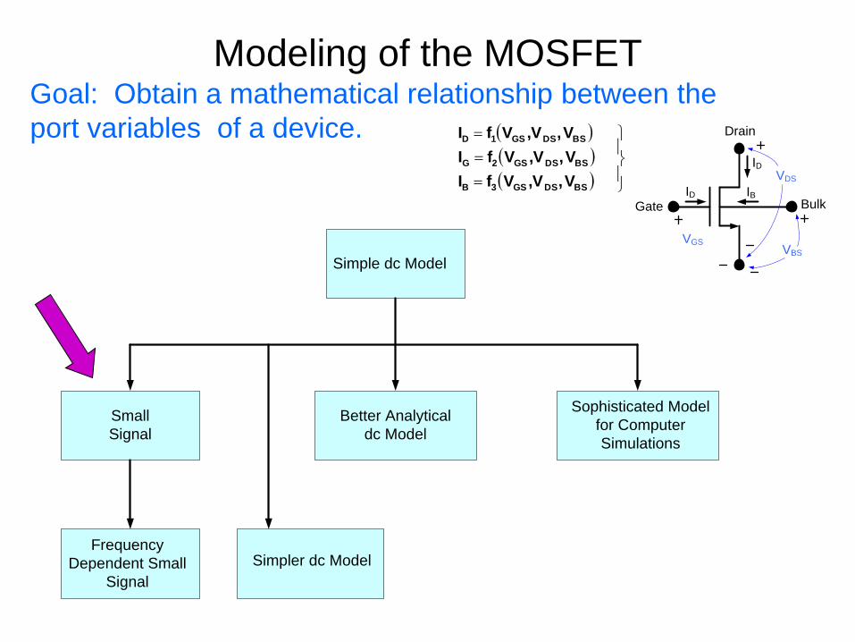
Modeling of the MOSFET
Drain
Gate Bulk
ID
ID IB
VDS
VBS
VGS
Goal: Obtain a mathematical relationship between the
port variables of a device.
Simple dc Model
Small
Signal
Frequency
Dependent Small
Signal
Better Analytical
dc Model
Sophisticated Model
for Computer
Simulations
Simpler dc Model
BSDSGS3B
BSDSGS2G
BSDSGS1D
V,,VVfI
V,,VVfI
V,,VVfI
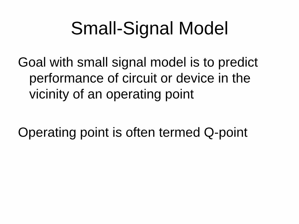
Small-Signal Model
Goal with small signal model is to predict
performance of circuit or device in the
vicinity of an operating point
Operating point is often termed Q-point
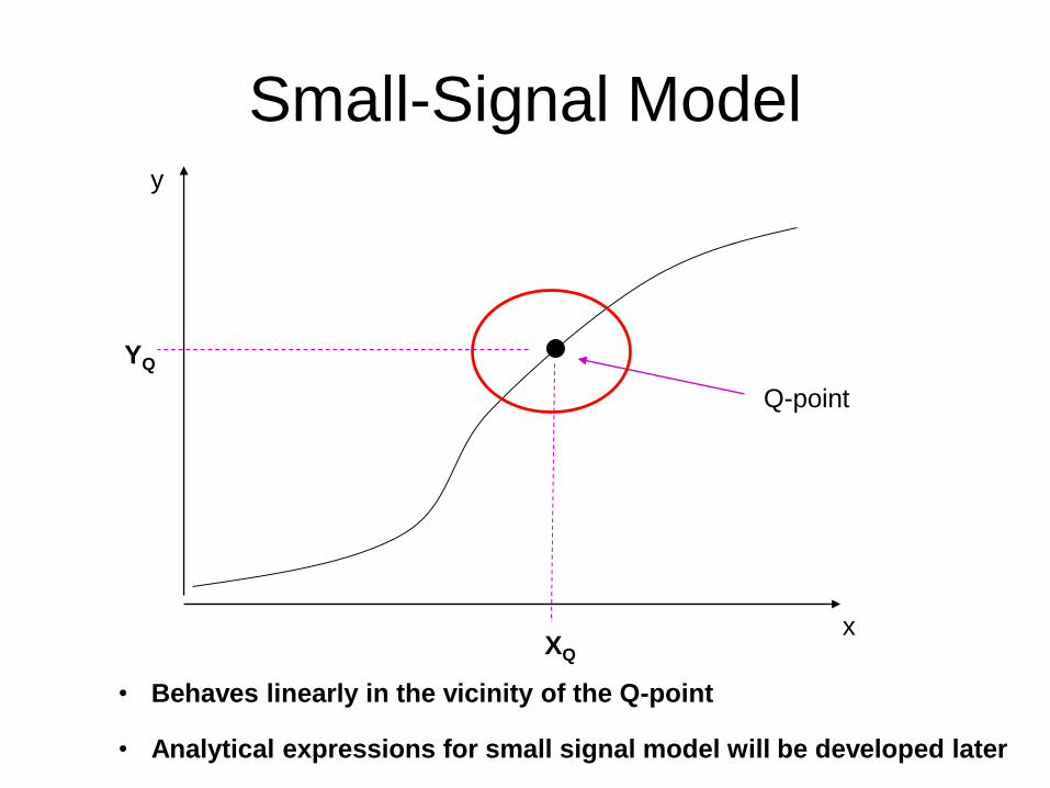
Small-Signal Modely
x
Q-point
XQ
YQ
• Analytical expressions for small signal model will be developed later
• Behaves linearly in the vicinity of the Q-point

Stay Safe and Stay Healthy !
End of Lecture 17