Operating Points for Amplifier Applications Amplification ...class.ece.iastate.edu/ee330/lectures/EE...
38
EE 330 Lecture 20 • Operating Points for Amplifier Applications • Amplification with Transistor Circuits • Small Signal Modelling
Transcript of Operating Points for Amplifier Applications Amplification ...class.ece.iastate.edu/ee330/lectures/EE...
EE 330
Lecture 20
• Operating Points for Amplifier Applications
• Amplification with Transistor Circuits
• Small Signal Modelling
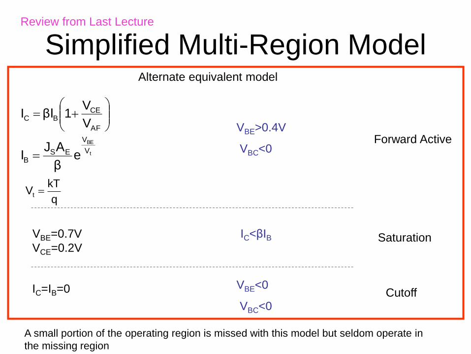
Simplified Multi-Region Model
AF
CEBC
V
V1βII
t
BE
V
V
ESB e
β
AJI
q
kTVt
VBE=0.7V
VCE=0.2V
IC=IB=0
Forward Active
Saturation
Cutoff
VBE>0.4V
VBC<0
IC<βIB
VBE<0
VBC<0
A small portion of the operating region is missed with this model but seldom operate in
the missing region
Alternate equivalent model
Review from Last Lecture
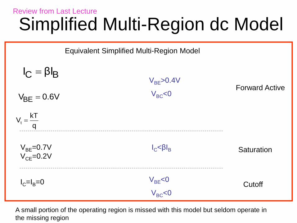
Simplified Multi-Region dc Model
Equivalent Simplified Multi-Region Model
C BI βI
BEV 0.6V
q
kTVt
VBE=0.7V
VCE=0.2V
IC=IB=0
Forward Active
Saturation
Cutoff
VBE>0.4V
VBC<0
IC<βIB
VBE<0
VBC<0
A small portion of the operating region is missed with this model but seldom operate in
the missing region
Review from Last Lecture
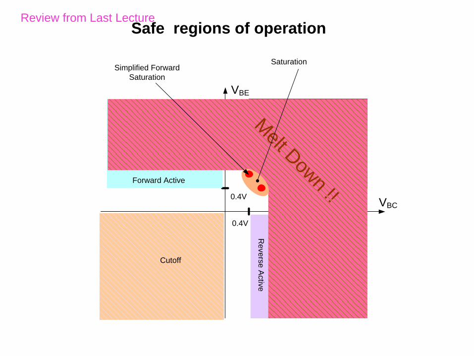
Safe regions of operation
VBC
VBE
0.4V
0.4V
Forward Active
Cutoff
Re
ve
rse
Activ
e
Saturation
Melt D
own !!
SaturationSimplified Forward
Saturation
Review from Last Lecture
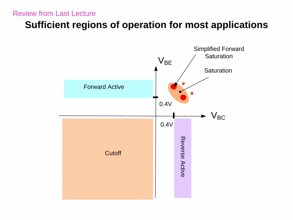
Sufficient regions of operation for most applications
VBC
VBE
0.4V
0.4V
Forward Active
Cutoff
Re
ve
rse
Activ
e
Saturation
Simplified Forward
Saturation
Review from Last Lecture
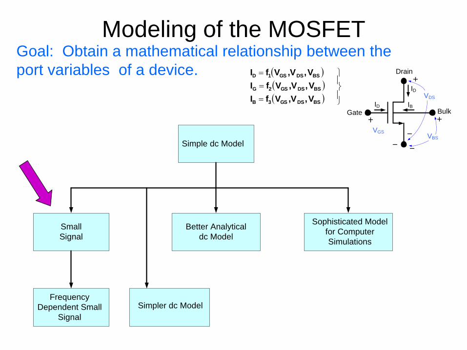
Modeling of the MOSFET
Drain
Gate Bulk
ID
ID IB
VDS
VBS
VGS
Goal: Obtain a mathematical relationship between the
port variables of a device.
Simple dc Model
Small
Signal
Frequency
Dependent Small
Signal
Better Analytical
dc Model
Sophisticated Model
for Computer
Simulations
Simpler dc Model
BSDSGS3B
BSDSGS2G
BSDSGS1D
V,,VVfI
V,,VVfI
V,,VVfI
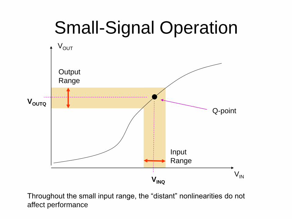
Small-Signal Operation
VIN
Q-point
VINQ
VOUTQ
VOUT
Input
Range
Output
Range
Throughout the small input range, the “distant” nonlinearities do not
affect performance
Small-Signal Operation
VIN
Q-point
VINQ
VOUTQ
VOUT
Input
Range
Output
Range
• If slope is steep, output range can be much larger than input range
• The slope can be viewed as the voltage gain of the circuit
• Nonlinear circuit behaves as a linear circuit near Q-point with small-signal
inputs
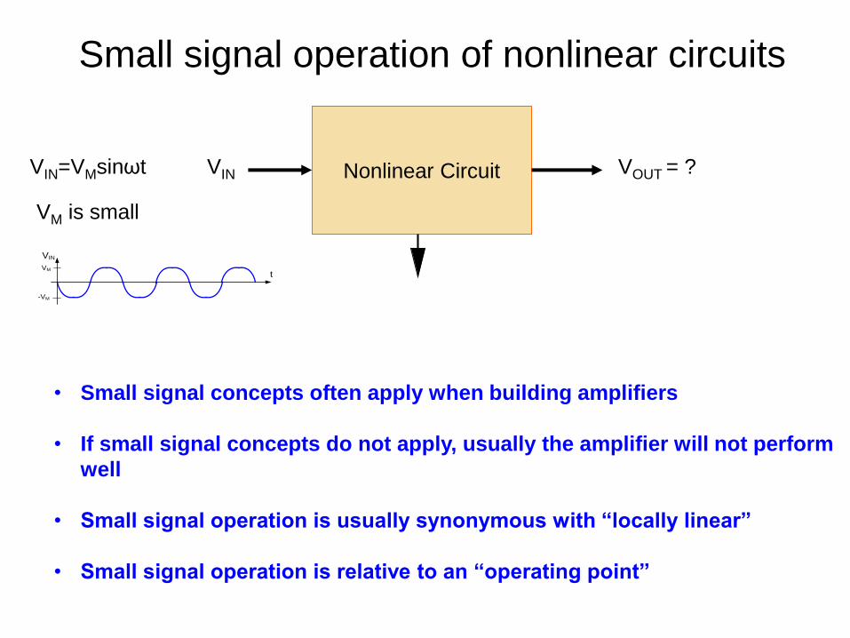
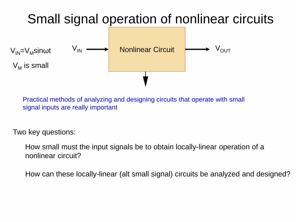
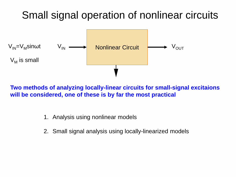
Small signal operation of nonlinear circuits
VIN=VMsinωt
VM is small
Nonlinear CircuitVIN VOUT = ?
VIN
tVM
-VM
• Small signal concepts often apply when building amplifiers
• If small signal concepts do not apply, usually the amplifier will not perform
well
• Small signal operation is usually synonymous with “locally linear”
• Small signal operation is relative to an “operating point”
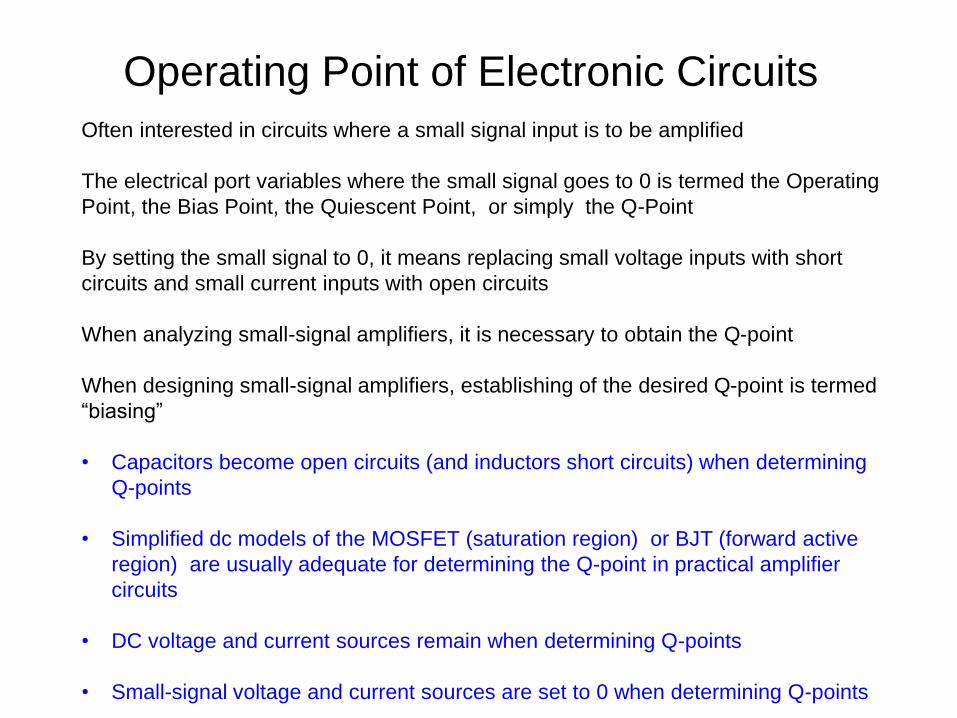
Operating Point of Electronic Circuits
Often interested in circuits where a small signal input is to be amplified
The electrical port variables where the small signal goes to 0 is termed the Operating
Point, the Bias Point, the Quiescent Point, or simply the Q-Point
By setting the small signal to 0, it means replacing small voltage inputs with short
circuits and small current inputs with open circuits
When analyzing small-signal amplifiers, it is necessary to obtain the Q-point
When designing small-signal amplifiers, establishing of the desired Q-point is termed
“biasing”
• Capacitors become open circuits (and inductors short circuits) when determining
Q-points
• Simplified dc models of the MOSFET (saturation region) or BJT (forward active
region) are usually adequate for determining the Q-point in practical amplifier
circuits
• DC voltage and current sources remain when determining Q-points
• Small-signal voltage and current sources are set to 0 when determining Q-points
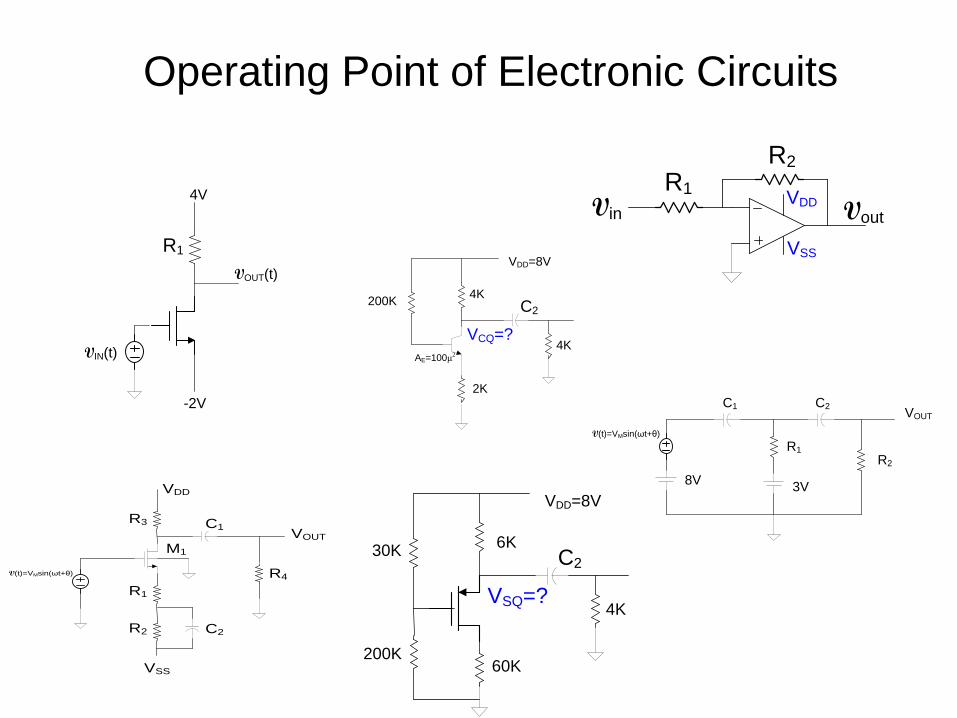
Operating Point of Electronic Circuits
VDD=8V
4K
C2
VSQ=?
30K
200K60K
6K
VDD=8V
4K
4K
C2
VCQ=?
2K
200K
AE=100μ2
R1
C1 C2
R2
3V8V
V(t)=VMsin(ωt+θ)
VOUT
M1
VDD
R3
R4
C1VOUT
V(t)=VMsin(ωt+θ)
VSS
R1
R2 C2
VIN(t)
R1
-2V
4V
VOUT(t)
Vin Vout
R2
R1
VSS
VDD
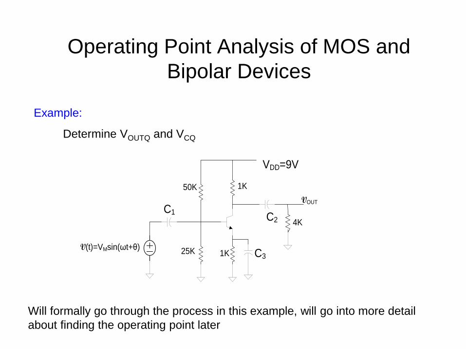
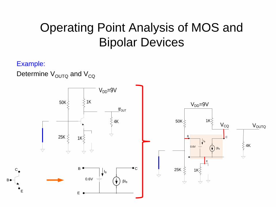
Operating Point Analysis of MOS and
Bipolar Devices
25KV(t)=VMsin(ωt+θ)
50K
VDD=9V
VOUT
1K
4K
1K
C1C2
C3
Determine VOUTQ and VCQ
Example:
Will formally go through the process in this example, will go into more detail
about finding the operating point later
Operating Point Analysis of MOS and
Bipolar Devices
25K
50K
VDD=9V
VOUT
1K
4K
1K
Determine VOUTQ and VCQ
Example:
βIB
IBB C
E
0.6V
E
B
C 25K
50K
VDD=9V
1K
4K
1K
βIB
IB
C
0.6V
B
E
VOUTQVCQ
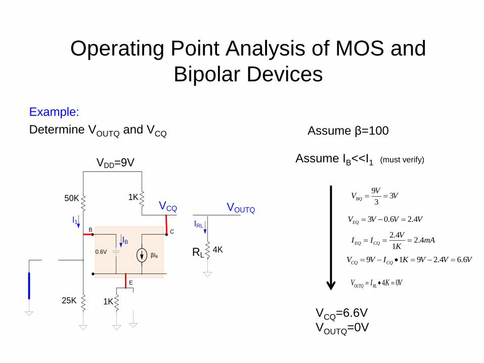
Operating Point Analysis of MOS and
Bipolar Devices
Determine VOUTQ and VCQ
Example:
25K
50K
VDD=9V
1K
4K
1K
βIB
IB
C
0.6V
B
E
VOUTQVCQ
I1
RL
IRL
Assume β=100
Assume IB<<I1 (must verify)
VCQ=6.6V
VOUTQ=0V
93
3BQ
VV V
3 0.6 2.4EQV V V V
2.42.4
1EQ CQ
VI I mA
K
9 1 9 2.4 6.6CQ CQV V I K V V V
4 0OUTQ RLV I K V
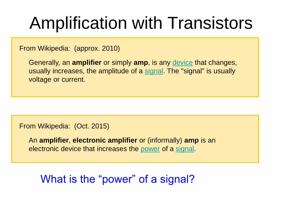
Amplification with Transistors
Generally, an amplifier or simply amp, is any device that changes,
usually increases, the amplitude of a signal. The "signal" is usually
voltage or current.
From Wikipedia: (approx. 2010)
An amplifier, electronic amplifier or (informally) amp is an
electronic device that increases the power of a signal.
From Wikipedia: (Oct. 2015)
What is the “power” of a signal?
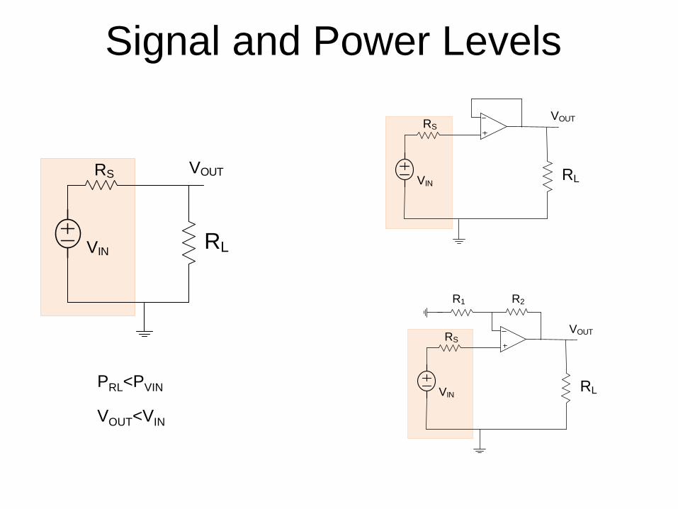
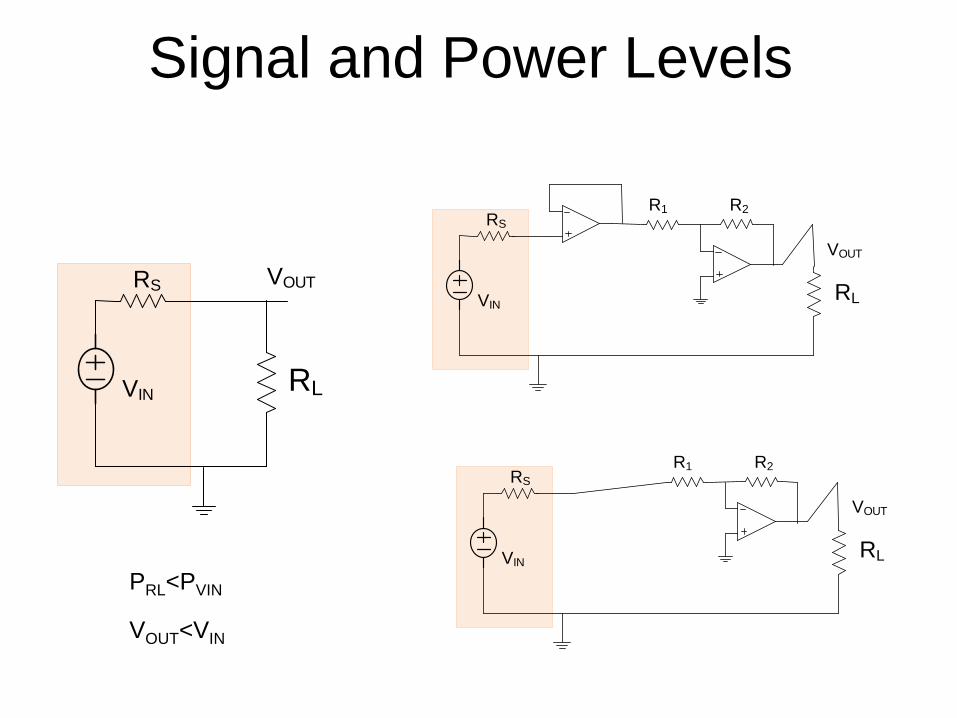
Signal and Power Levels
RL
RS
VIN
VOUT RL
RS
VIN
VOUT
RL
RS
VIN
VOUT
R2R1
PRL<PVIN
VOUT<VIN
Signal and Power Levels
RL
RS
VIN
VOUTRL
RS
VIN
VOUT
R2R1
RL
RS
VIN
VOUT
R2R1
PRL<PVIN
VOUT<VIN
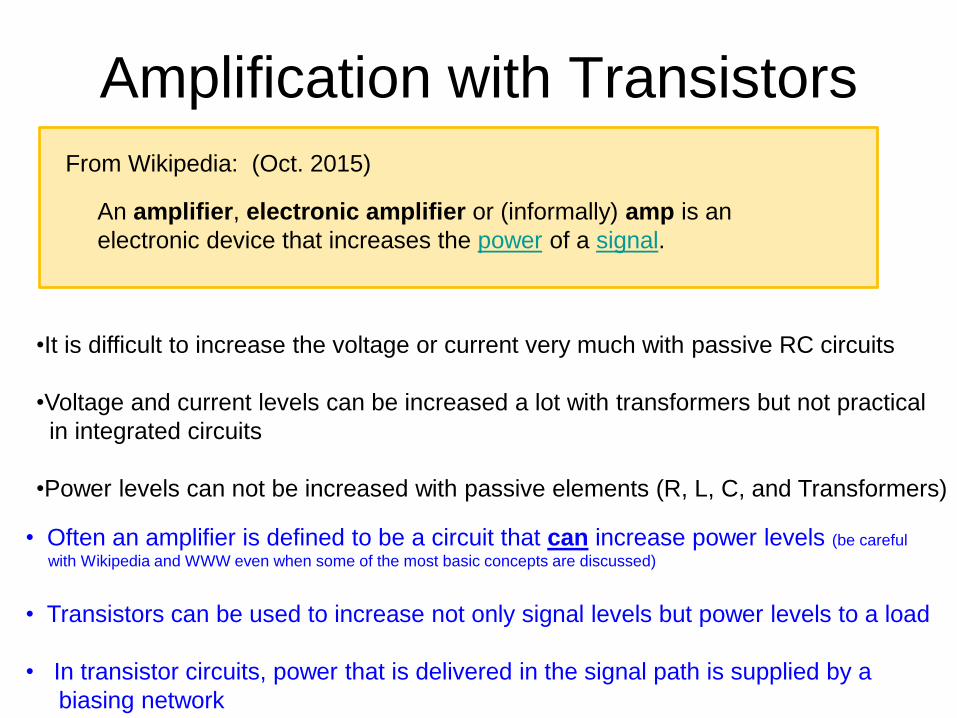
Amplification with Transistors
An amplifier, electronic amplifier or (informally) amp is an
electronic device that increases the power of a signal.
From Wikipedia: (Oct. 2015)
•It is difficult to increase the voltage or current very much with passive RC circuits
•Voltage and current levels can be increased a lot with transformers but not practical
in integrated circuits
•Power levels can not be increased with passive elements (R, L, C, and Transformers)
• Often an amplifier is defined to be a circuit that can increase power levels (be careful
with Wikipedia and WWW even when some of the most basic concepts are discussed)
• Transistors can be used to increase not only signal levels but power levels to a load
• In transistor circuits, power that is delivered in the signal path is supplied by a
biasing network
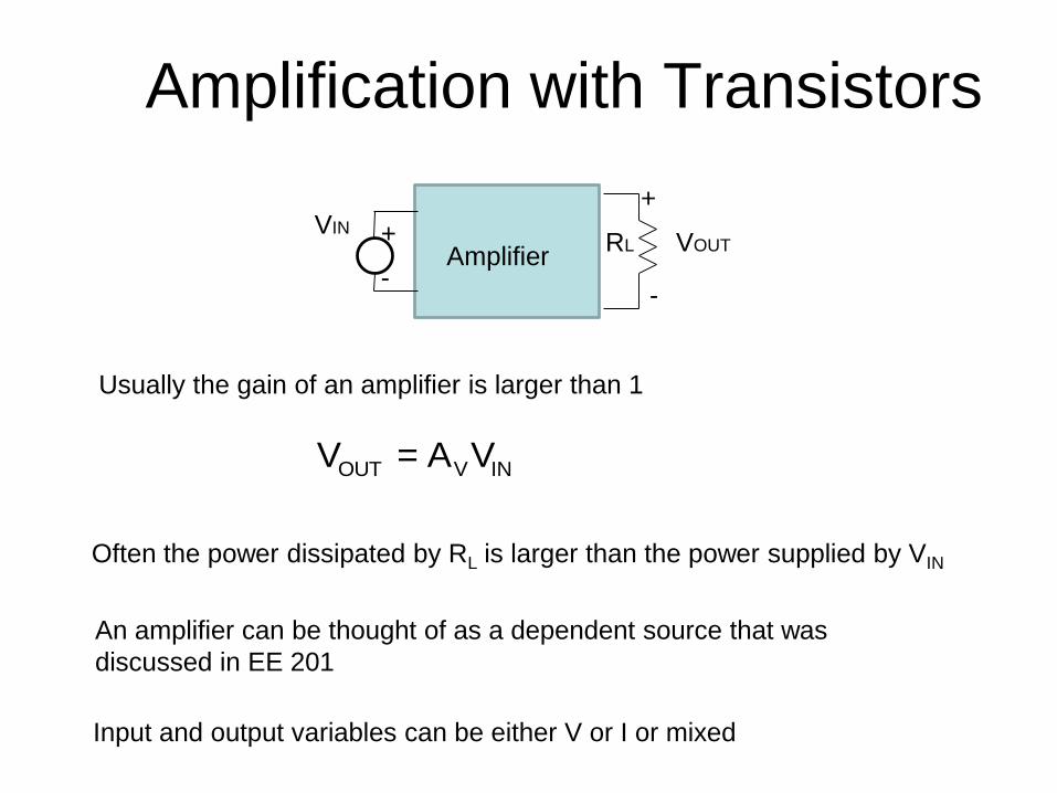
Amplification with Transistors
VINVOUTRL
+
-
Amplifier
Usually the gain of an amplifier is larger than 1
OUT V INV = A V
Often the power dissipated by RL is larger than the power supplied by VIN
An amplifier can be thought of as a dependent source that was
discussed in EE 201
Input and output variables can be either V or I or mixed
+
-
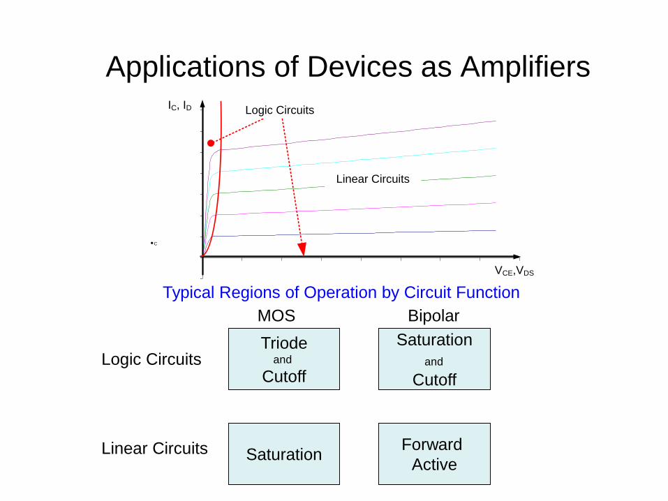
Applications of Devices as Amplifiers
MOS Bipolar
Logic Circuits
Linear Circuits
Triodeand
Cutoff
Saturation
and
Cutoff
SaturationForward
Active
Typical Regions of Operation by Circuit Function
C
VCE,VDS
IC, ID
Linear Circuits
Logic Circuits
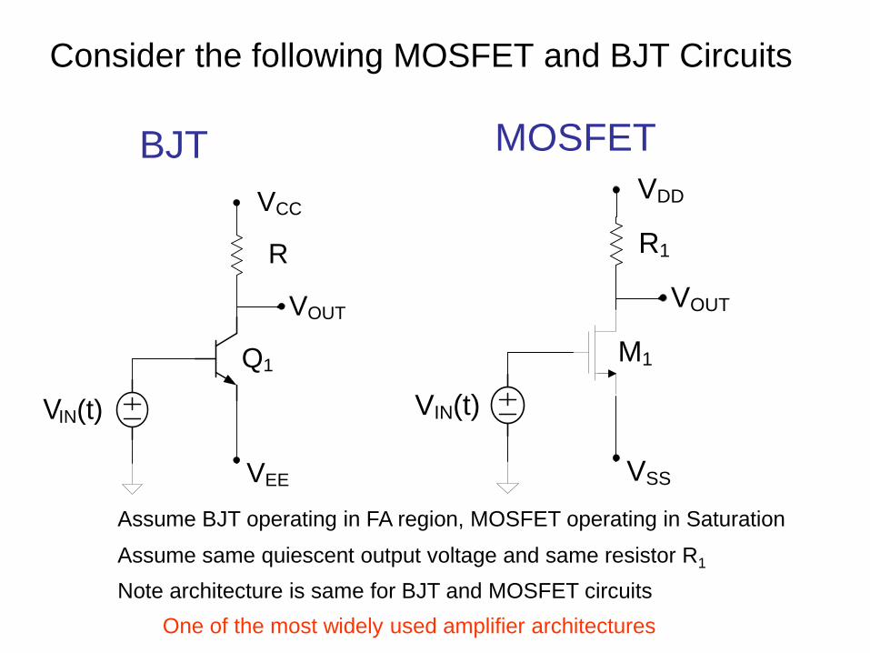
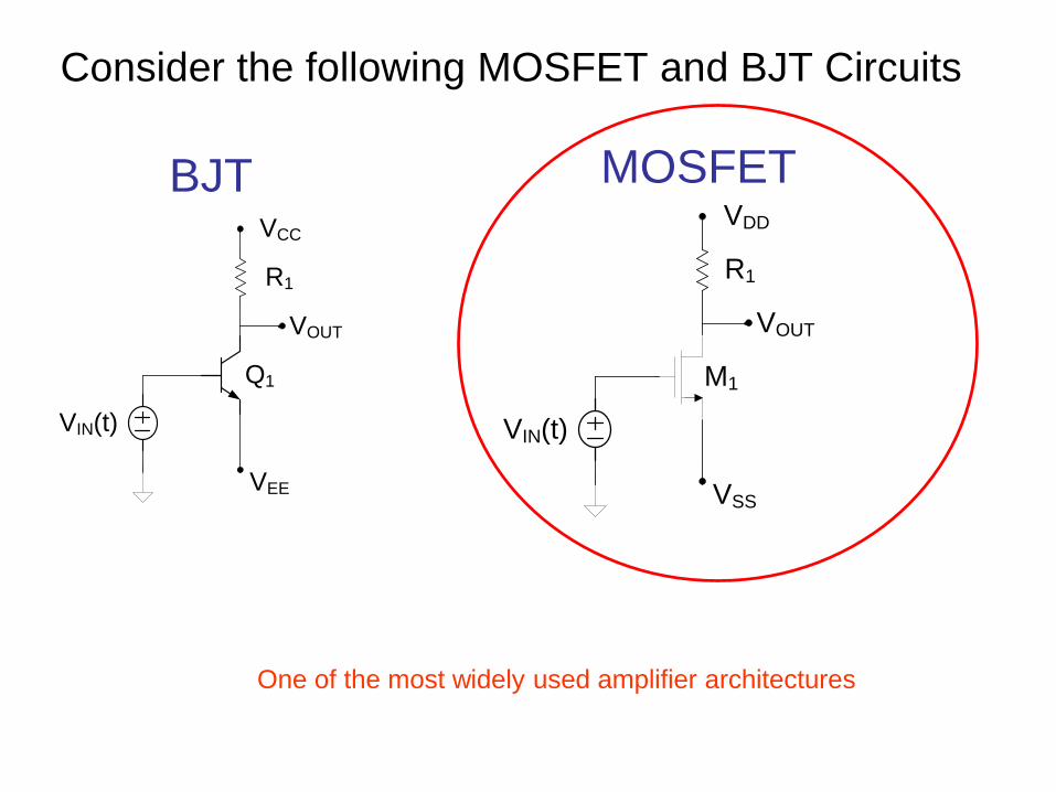
Consider the following MOSFET and BJT Circuits
R
Q1
VIN(t)
VOUT
VCC
VEE
BJT MOSFET
R1
VIN(t)
VOUT
VDD
VSS
M1
Assume BJT operating in FA region, MOSFET operating in Saturation
Assume same quiescent output voltage and same resistor R1
One of the most widely used amplifier architectures
Note architecture is same for BJT and MOSFET circuits
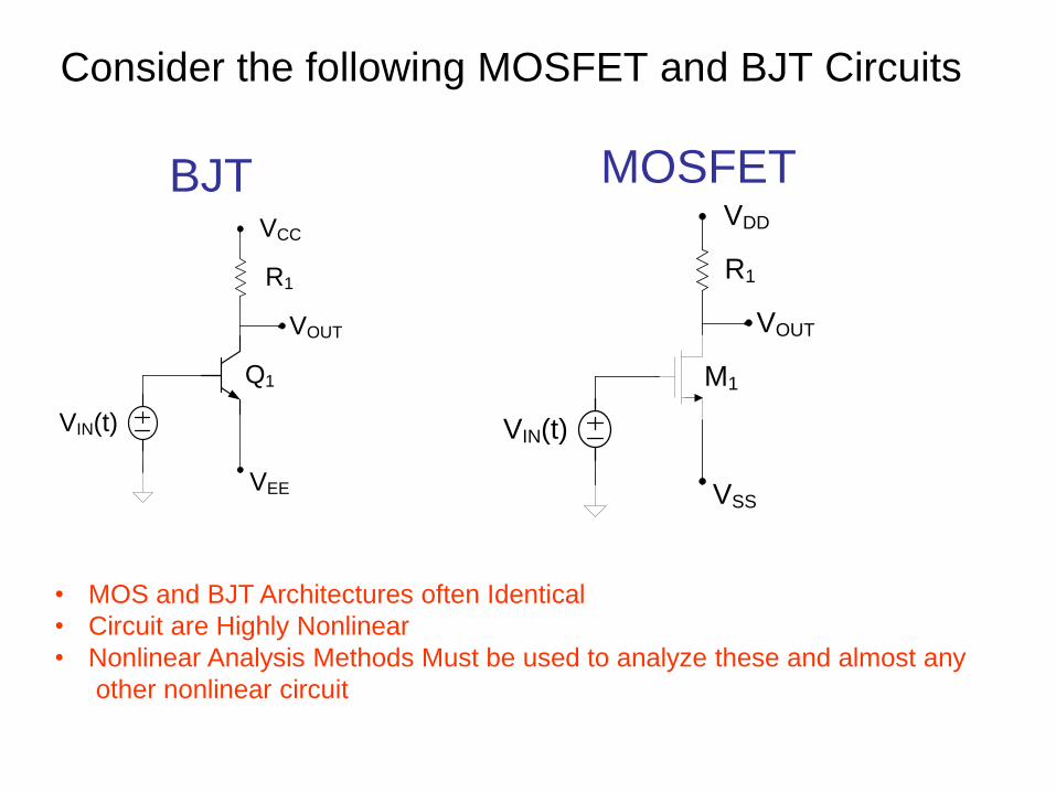
Consider the following MOSFET and BJT Circuits
R1
Q1
VIN(t)
VOUT
VCC
VEE
BJT MOSFET
R1
VIN(t)
VOUT
VDD
VSS
M1
• MOS and BJT Architectures often Identical
• Circuit are Highly Nonlinear
• Nonlinear Analysis Methods Must be used to analyze these and almost any
other nonlinear circuit
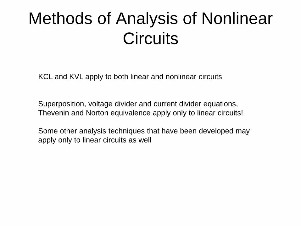
Methods of Analysis of Nonlinear
Circuits
KCL and KVL apply to both linear and nonlinear circuits
Superposition, voltage divider and current divider equations,
Thevenin and Norton equivalence apply only to linear circuits!
Some other analysis techniques that have been developed may
apply only to linear circuits as well
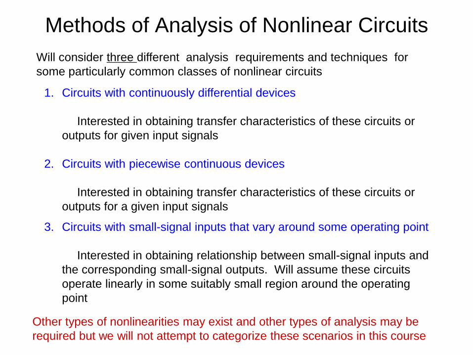
Methods of Analysis of Nonlinear Circuits
Will consider three different analysis requirements and techniques for
some particularly common classes of nonlinear circuits
1. Circuits with continuously differential devices
Interested in obtaining transfer characteristics of these circuits or
outputs for given input signals
2. Circuits with piecewise continuous devices
Interested in obtaining transfer characteristics of these circuits or
outputs for a given input signals
3. Circuits with small-signal inputs that vary around some operating point
Interested in obtaining relationship between small-signal inputs and
the corresponding small-signal outputs. Will assume these circuits
operate linearly in some suitably small region around the operating
point
Other types of nonlinearities may exist and other types of analysis may be
required but we will not attempt to categorize these scenarios in this course
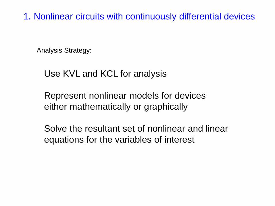
1. Nonlinear circuits with continuously differential devices
Use KVL and KCL for analysis
Represent nonlinear models for devices
either mathematically or graphically
Solve the resultant set of nonlinear and linear
equations for the variables of interest
Analysis Strategy:
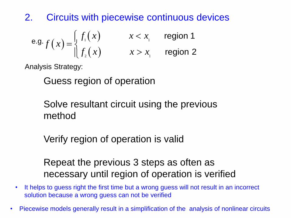
2. Circuits with piecewise continuous devices
e.g.
1 1
2 1
region 1
region 2
f x x xf x
f x x x
Analysis Strategy:
Guess region of operation
Solve resultant circuit using the previous
method
Verify region of operation is valid
Repeat the previous 3 steps as often as
necessary until region of operation is verified
• It helps to guess right the first time but a wrong guess will not result in an incorrect
solution because a wrong guess can not be verified
• Piecewise models generally result in a simplification of the analysis of nonlinear circuits
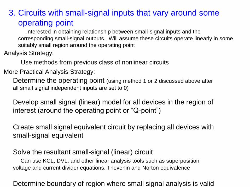
3. Circuits with small-signal inputs that vary around some
operating point Interested in obtaining relationship between small-signal inputs and the
corresponding small-signal outputs. Will assume these circuits operate linearly in some
suitably small region around the operating point
More Practical Analysis Strategy:
Determine the operating point (using method 1 or 2 discussed above after
all small signal independent inputs are set to 0)
Develop small signal (linear) model for all devices in the region of
interest (around the operating point or “Q-point”)
Create small signal equivalent circuit by replacing all devices with
small-signal equivalent
Solve the resultant small-signal (linear) circuit
Can use KCL, DVL, and other linear analysis tools such as superposition,
voltage and current divider equations, Thevenin and Norton equivalence
Determine boundary of region where small signal analysis is valid
Analysis Strategy:
Use methods from previous class of nonlinear circuits
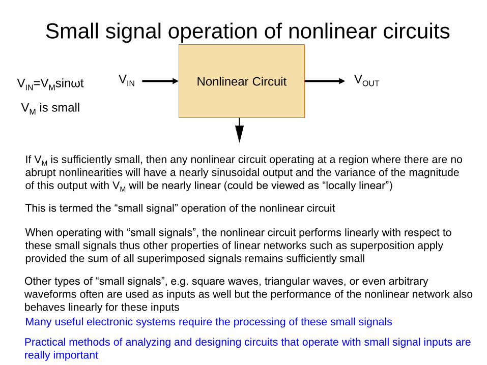
Small signal operation of nonlinear circuits
VIN=VMsinωt
VM is small
Nonlinear CircuitVIN VOUT
If VM is sufficiently small, then any nonlinear circuit operating at a region where there are no
abrupt nonlinearities will have a nearly sinusoidal output and the variance of the magnitude
of this output with VM will be nearly linear (could be viewed as “locally linear”)
This is termed the “small signal” operation of the nonlinear circuit
Many useful electronic systems require the processing of these small signals
Other types of “small signals”, e.g. square waves, triangular waves, or even arbitrary
waveforms often are used as inputs as well but the performance of the nonlinear network also
behaves linearly for these inputs
When operating with “small signals”, the nonlinear circuit performs linearly with respect to
these small signals thus other properties of linear networks such as superposition apply
provided the sum of all superimposed signals remains sufficiently small
Practical methods of analyzing and designing circuits that operate with small signal inputs are
really important
Small signal operation of nonlinear circuits
VIN=VMsinωt
VM is small
Nonlinear CircuitVIN VOUT
Practical methods of analyzing and designing circuits that operate with small
signal inputs are really important
Two key questions:
How small must the input signals be to obtain locally-linear operation of a
nonlinear circuit?
How can these locally-linear (alt small signal) circuits be analyzed and designed?
Consider the following MOSFET and BJT Circuits
R1
Q1
VIN(t)
VOUT
VCC
VEE
BJT MOSFET
R1
VIN(t)
VOUT
VDD
VSS
M1
One of the most widely used amplifier architectures
Small signal operation of nonlinear circuits
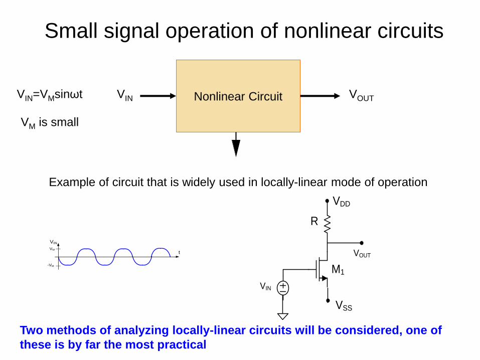
VDD
R
M1
VIN
VOUT
VSS
VIN=VMsinωt
VM is small
Nonlinear CircuitVIN VOUT
VIN
tVM
-VM
Example of circuit that is widely used in locally-linear mode of operation
Two methods of analyzing locally-linear circuits will be considered, one of
these is by far the most practical
Small signal operation of nonlinear circuits
VIN=VMsinωt
VM is small
Nonlinear CircuitVIN VOUT
Two methods of analyzing locally-linear circuits for small-signal excitaions
will be considered, one of these is by far the most practical
1. Analysis using nonlinear models
2. Small signal analysis using locally-linearized models
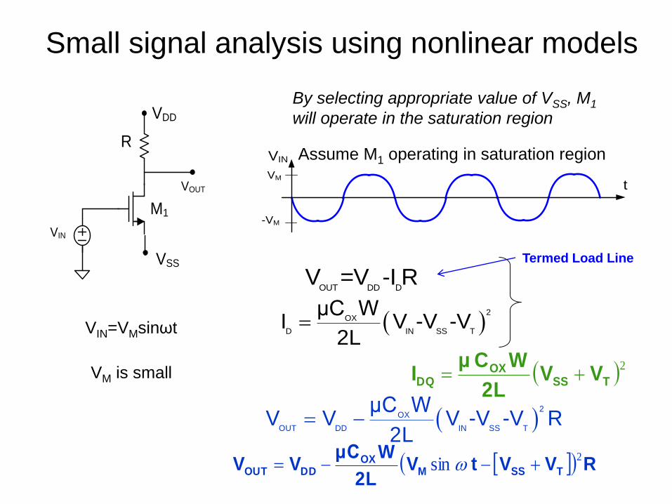
Small signal analysis using nonlinear models
RVVtV2L
WμCVV TSSM
OXDDOUT
2sin
VDD
R
M1
VIN
VOUT
VSS
Assume M1 operating in saturation region
By selecting appropriate value of VSS, M1
will operate in the saturation region
VIN=VMsinωt
VM is small
VIN
tVM
-VM
2
OX
D IN SS T
μC WI V -V -V
2L
OUT DD DV =V -I R
2
OX
OUT DD IN SS T
μC WV V V -V -V R
2L
2TSSOX
DQ VV2L
WC μI
Termed Load Line
Small signal analysis example
RVVtV2L
WμCVV TSSM
OXDDOUT
2sin
VDD
R
M1
VIN
VOUT
VSS
VIN=VMsinωt
VM is small
RVV
tV1-VV
2L
WμCVV
TSS
MTSS
OXDDOUT
2
2 sin
Recall that if x is small 2
1+x 1+2x
2 sinOX MOUT DD SS T
SS T
μC W 2V tV V V V 1- R
2L V V
2 2OX OX M
OUT DD SS T SS T
SS T
μC W μC W 2V sin tV V V V R V V R
2L 2L V V
2
OX OX
OUT DD SS T SS T M
μC W μC WV V V V R V V R V sin t
2L L
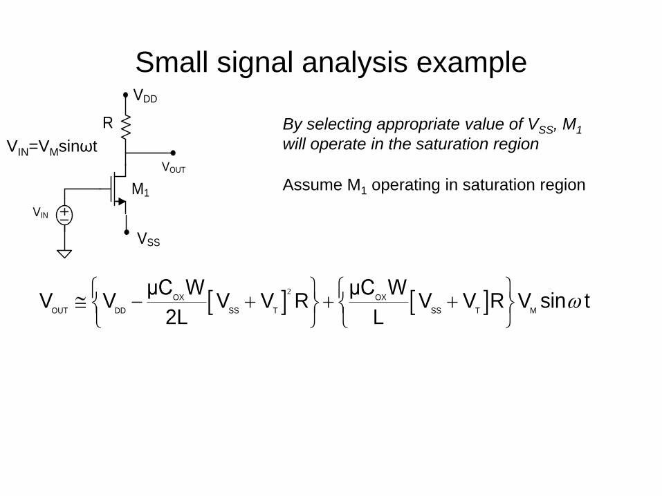
Small signal analysis exampleVDD
R
M1
VIN
VOUT
VSS
VIN=VMsinωt
2
OX OX
OUT DD SS T SS T M
μC W μC WV V V V R V V R V sin t
2L L
By selecting appropriate value of VSS, M1
will operate in the saturation region
Assume M1 operating in saturation region
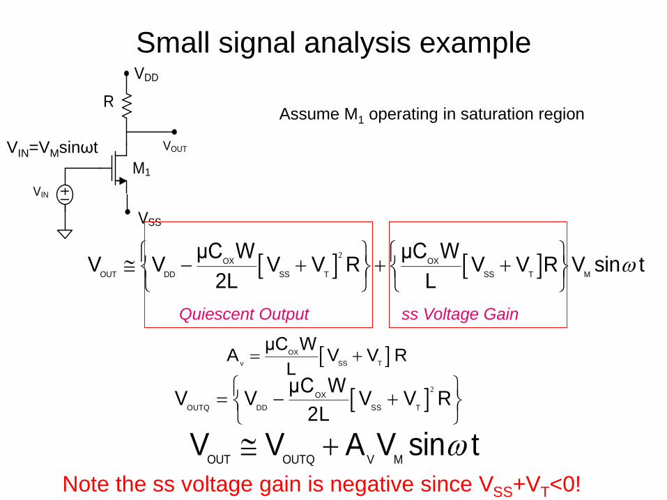
Small signal analysis exampleVDD
R
M1
VIN
VOUT
VSS
VIN=VMsinωt
2
OX OX
OUT DD SS T SS T M
μC W μC WV V V V R V V R V sin t
2L L
Quiescent Output ss Voltage Gain
OX
v SS T
μC WA V V R
L
Assume M1 operating in saturation region
2
OX
OUTQ DD SS T
μC WV V V V R
2L
OUT OUTQ V MV V A V sin t
Note the ss voltage gain is negative since VSS+VT<0!
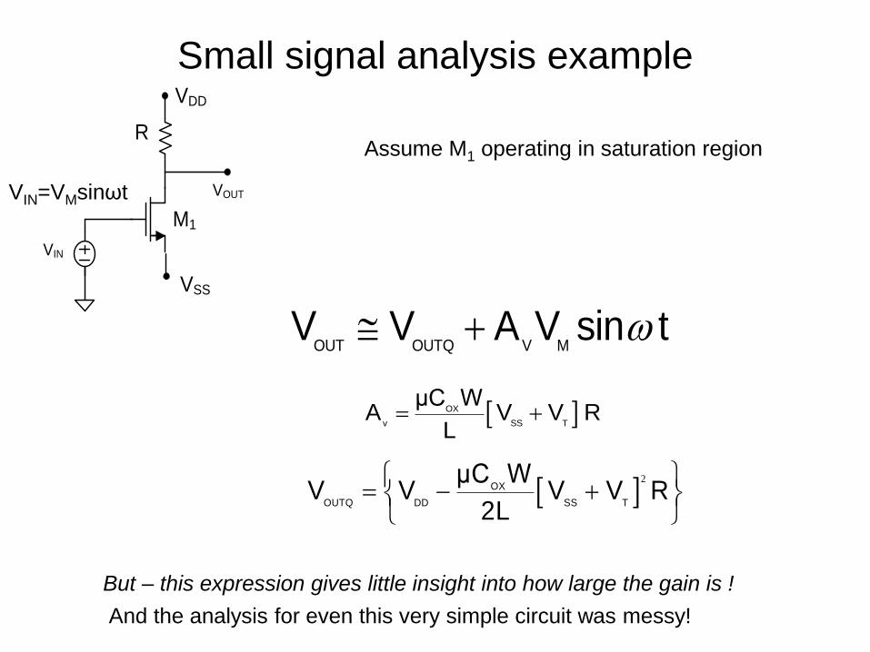
Small signal analysis exampleVDD
R
M1
VIN
VOUT
VSS
VIN=VMsinωt
OX
v SS T
μC WA V V R
L
But – this expression gives little insight into how large the gain is !
Assume M1 operating in saturation region
And the analysis for even this very simple circuit was messy!
2
OX
OUTQ DD SS T
μC WV V V V R
2L
OUT OUTQ V MV V A V sin t

End of Lecture 20