
(TOP VIEW) DD SHUTDOWN V - Analog, Embedded … · SLOS230D − NOVEMBER 1998 − REVISED OCTOBER...
39
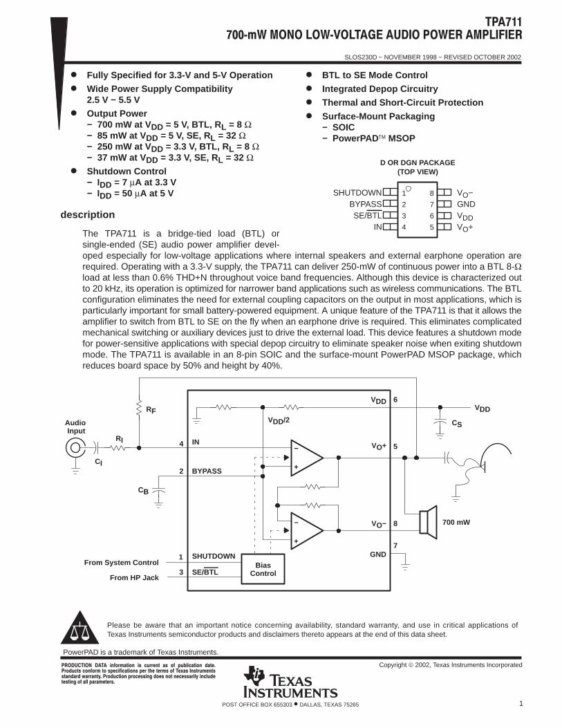
TPA711 700ĆmW MONO LOWĆVOLTAGE AUDIO POWER AMPLIFIER SLOS230D - NOVEMBER 1998 - REVISED OCTOBER 2002 1 POST OFFICE BOX 655303 • DALLAS, TEXAS 75265 D Fully Specified for 3.3-V and 5-V Operation D Wide Power Supply Compatibility 2.5 V - 5.5 V D Output Power - 700 mW at V DD = 5 V, BTL, R L = 8 Ω - 85 mW at V DD = 5 V, SE, R L = 32 Ω - 250 mW at V DD = 3.3 V, BTL, R L = 8 Ω - 37 mW at V DD = 3.3 V, SE, R L = 32 Ω D Shutdown Control - I DD = 7 µA at 3.3 V - I DD = 50 µA at 5 V D BTL to SE Mode Control D Integrated Depop Circuitry D Thermal and Short-Circuit Protection D Surface-Mount Packaging - SOIC - PowerPAD MSOP description The TPA711 is a bridge-tied load (BTL) or single-ended (SE) audio power amplifier devel- oped especially for low-voltage applications where internal speakers and external earphone operation are required. Operating with a 3.3-V supply, the TPA711 can deliver 250-mW of continuous power into a BTL 8-Ω load at less than 0.6% THD+N throughout voice band frequencies. Although this device is characterized out to 20 kHz, its operation is optimized for narrower band applications such as wireless communications. The BTL configuration eliminates the need for external coupling capacitors on the output in most applications, which is particularly important for small battery-powered equipment. A unique feature of the TPA711 is that it allows the amplifier to switch from BTL to SE on the fly when an earphone drive is required. This eliminates complicated mechanical switching or auxiliary devices just to drive the external load. This device features a shutdown mode for power-sensitive applications with special depop circuitry to eliminate speaker noise when exiting shutdown mode. The TPA711 is available in an 8-pin SOIC and the surface-mount PowerPAD MSOP package, which reduces board space by 50% and height by 40%. Audio Input Bias Control V DD 700 mW 6 5 7 V O + V DD 3 1 2 4 BYPASS IN SE/BTL V DD /2 C I R I C S C B R F SHUTDOWN From HP Jack V O - 8 GND From System Control - + - + Please be aware that an important notice concerning availability, standard warranty, and use in critical applications of Texas Instruments semiconductor products and disclaimers thereto appears at the end of this data sheet. Copyright 2002, Texas Instruments Incorporated PRODUCTION DATA information is current as of publication date. Products conform to specifications per the terms of Texas Instruments standard warranty. Production processing does not necessarily include testing of all parameters. 1 2 3 4 8 7 6 5 SHUTDOWN BYPASS SE/BTL IN V O - GND V DD V O + D OR DGN PACKAGE (TOP VIEW) PowerPAD is a trademark of Texas Instruments.
Transcript of (TOP VIEW) DD SHUTDOWN V - Analog, Embedded … · SLOS230D − NOVEMBER 1998 − REVISED OCTOBER...
SLOS230D − NOVEMBER 1998 − REVISED OCTOBER 2002
1POST OFFICE BOX 655303 • DALLAS, TEXAS 75265
Fully Specified for 3.3-V and 5-V Operation
Wide Power Supply Compatibility2.5 V − 5.5 V
Output Power− 700 mW at VDD = 5 V, BTL, RL = 8 Ω− 85 mW at VDD = 5 V, SE, RL = 32 Ω− 250 mW at VDD = 3.3 V, BTL, RL = 8 Ω− 37 mW at VDD = 3.3 V, SE, RL = 32 Ω
Shutdown Control− IDD = 7 µA at 3.3 V− IDD = 50 µA at 5 V
BTL to SE Mode Control
Integrated Depop Circuitry
Thermal and Short-Circuit Protection
Surface-Mount Packaging− SOIC− PowerPAD MSOP
description
The TPA711 is a bridge-tied load (BTL) orsingle-ended (SE) audio power amplifier devel-oped especially for low-voltage applications where internal speakers and external earphone operation arerequired. Operating with a 3.3-V supply, the TPA711 can deliver 250-mW of continuous power into a BTL 8-Ωload at less than 0.6% THD+N throughout voice band frequencies. Although this device is characterized outto 20 kHz, its operation is optimized for narrower band applications such as wireless communications. The BTLconfiguration eliminates the need for external coupling capacitors on the output in most applications, which isparticularly important for small battery-powered equipment. A unique feature of the TPA711 is that it allows theamplifier to switch from BTL to SE on the fly when an earphone drive is required. This eliminates complicatedmechanical switching or auxiliary devices just to drive the external load. This device features a shutdown modefor power-sensitive applications with special depop circuitry to eliminate speaker noise when exiting shutdownmode. The TPA711 is available in an 8-pin SOIC and the surface-mount PowerPAD MSOP package, whichreduces board space by 50% and height by 40%.
Audio Input
BiasControl
VDD
700 mW
6
5
7
VO+
VDD
3
1
2
4
BYPASS
IN
SE/BTL
VDD/2
CI
RI
CS
CB
RF
SHUTDOWN
From HP Jack
VO− 8
GNDFrom System Control
−
+
−
+
Please be aware that an important notice concerning availability, standard warranty, and use in critical applications ofTexas Instruments semiconductor products and disclaimers thereto appears at the end of this data sheet.
Copyright 2002, Texas Instruments Incorporated !" #!$% &"'&! #" #" (" " ") !"&& *+' &! #", &" ""%+ %!&"", %% #""'
1
2
3
4
8
7
6
5
SHUTDOWNBYPASSSE/BTL
IN
VO−GNDVDDVO+
D OR DGN PACKAGE(TOP VIEW)
PowerPAD is a trademark of Texas Instruments.
SLOS230D − NOVEMBER 1998 − REVISED OCTOBER 2002
2 POST OFFICE BOX 655303 • DALLAS, TEXAS 75265
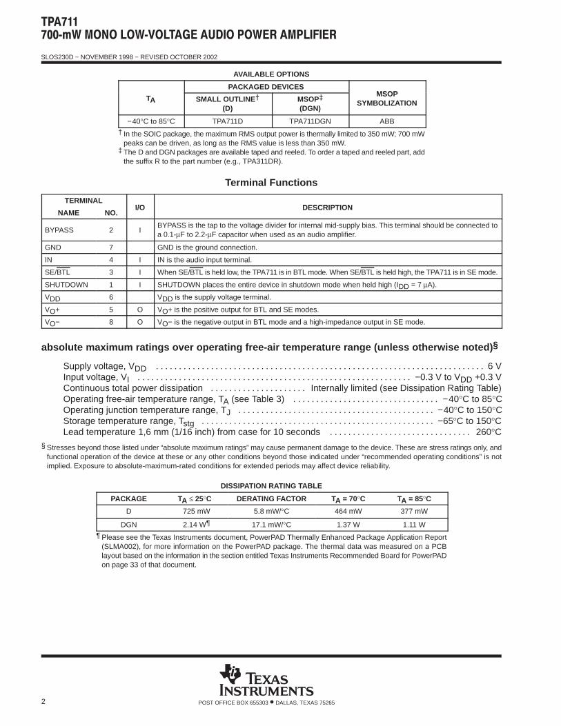
AVAILABLE OPTIONS
PACKAGED DEVICESMSOP
TA SMALL OUTLINE †
(D)MSOP‡
(DGN)
MSOPSYMBOLIZATION
−40°C to 85°C TPA711D TPA711DGN ABB
† In the SOIC package, the maximum RMS output power is thermally limited to 350 mW; 700 mWpeaks can be driven, as long as the RMS value is less than 350 mW.
‡ The D and DGN packages are available taped and reeled. To order a taped and reeled part, addthe suffix R to the part number (e.g., TPA311DR).
Terminal Functions
TERMINALI/O DESCRIPTION
NAME NO.I/O DESCRIPTION
BYPASS 2 IBYPASS is the tap to the voltage divider for internal mid-supply bias. This terminal should be connected toa 0.1-µF to 2.2-µF capacitor when used as an audio amplifier.
GND 7 GND is the ground connection.
IN 4 I IN is the audio input terminal.
SE/BTL 3 I When SE/BTL is held low, the TPA711 is in BTL mode. When SE/BTL is held high, the TPA711 is in SE mode.
SHUTDOWN 1 I SHUTDOWN places the entire device in shutdown mode when held high (IDD = 7 µA).
VDD 6 VDD is the supply voltage terminal.
VO+ 5 O VO+ is the positive output for BTL and SE modes.
VO− 8 O VO− is the negative output in BTL mode and a high-impedance output in SE mode.
absolute maximum ratings over operating free-air temperature range (unless otherwise noted) §
Supply voltage, VDD 6 V. . . . . . . . . . . . . . . . . . . . . . . . . . . . . . . . . . . . . . . . . . . . . . . . . . . . . . . . . . . . . . . . . . . . . . . . Input voltage, VI −0.3 V to VDD +0.3 V. . . . . . . . . . . . . . . . . . . . . . . . . . . . . . . . . . . . . . . . . . . . . . . . . . . . . . . . . . . . Continuous total power dissipation Internally limited (see Dissipation Rating Table). . . . . . . . . . . . . . . . . . . . . Operating free-air temperature range, TA (see Table 3) −40°C to 85°C. . . . . . . . . . . . . . . . . . . . . . . . . . . . . . . . Operating junction temperature range, TJ −40°C to 150°C. . . . . . . . . . . . . . . . . . . . . . . . . . . . . . . . . . . . . . . . . . . Storage temperature range, Tstg −65°C to 150°C. . . . . . . . . . . . . . . . . . . . . . . . . . . . . . . . . . . . . . . . . . . . . . . . . . . Lead temperature 1,6 mm (1/16 inch) from case for 10 seconds 260°C. . . . . . . . . . . . . . . . . . . . . . . . . . . . . . .
§ Stresses beyond those listed under “absolute maximum ratings” may cause permanent damage to the device. These are stress ratings only, andfunctional operation of the device at these or any other conditions beyond those indicated under “recommended operating conditions” is notimplied. Exposure to absolute-maximum-rated conditions for extended periods may affect device reliability.
DISSIPATION RATING TABLE
PACKAGE TA ≤ 25°C DERATING FACTOR TA = 70°C TA = 85°C
D 725 mW 5.8 mW/°C 464 mW 377 mW
DGN 2.14 W¶ 17.1 mW/°C 1.37 W 1.11 W
¶ Please see the Texas Instruments document, PowerPAD Thermally Enhanced Package Application Report(SLMA002), for more information on the PowerPAD package. The thermal data was measured on a PCBlayout based on the information in the section entitled Texas Instruments Recommended Board for PowerPADon page 33 of that document.
SLOS230D − NOVEMBER 1998 − REVISED OCTOBER 2002
3POST OFFICE BOX 655303 • DALLAS, TEXAS 75265
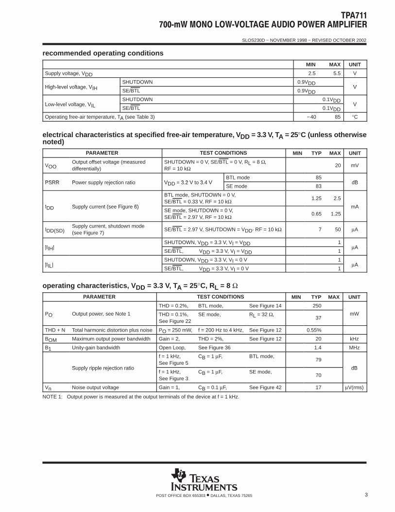
recommended operating conditions
MIN MAX UNITÁÁÁÁÁÁÁÁÁÁÁÁÁÁÁÁÁÁÁÁÁÁÁÁÁÁÁÁÁÁÁÁÁÁÁÁÁÁÁÁÁÁÁÁÁÁÁÁÁÁÁÁSupply voltage, VDD
ÁÁÁÁÁÁÁÁ2.5
ÁÁÁÁÁÁ5.5
ÁÁÁÁÁÁVÁÁÁÁÁÁÁÁÁ
ÁÁÁÁÁÁÁÁÁHigh-level voltage, VIHSHUTDOWN
ÁÁÁÁÁÁÁÁ
0.9VDDÁÁÁÁÁÁ
ÁÁÁÁÁÁVÁÁÁÁÁÁÁÁÁ
ÁÁÁÁÁÁÁÁÁHigh-level voltage, VIH SE/BTL
ÁÁÁÁÁÁÁÁ
0.9VDDÁÁÁÁÁÁ
ÁÁÁÁÁÁ
V
ÁÁÁÁÁÁÁÁÁÁÁÁÁÁÁÁÁÁLow-level voltage, VIL
SHUTDOWN ÁÁÁÁÁÁÁÁ
ÁÁÁÁÁÁ
0.1VDDÁÁÁÁÁÁVÁÁÁÁÁÁÁÁÁ
ÁÁÁÁÁÁÁÁÁ
Low-level voltage, VIL SE/BTL ÁÁÁÁÁÁÁÁ
ÁÁÁÁÁÁ
0.1VDDÁÁÁÁÁÁ
V
ÁÁÁÁÁÁÁÁÁÁÁÁÁÁÁÁÁÁÁÁÁÁÁÁÁÁÁÁÁÁÁÁÁÁÁÁÁÁÁÁÁÁÁÁÁÁÁÁÁÁÁÁ
Operating free-air temperature, TA (see Table 3) ÁÁÁÁÁÁÁÁ
−40ÁÁÁÁÁÁ
85ÁÁÁÁÁÁ
°C
electrical characteristics at specified free-air temperature, V DD = 3.3 V, TA = 25°C (unless otherwisenoted)
PARAMETER TEST CONDITIONS MIN TYP MAX UNITÁÁÁÁÁÁÁÁÁÁÁÁ
VOO
ÁÁÁÁÁÁÁÁÁÁÁÁÁÁÁÁÁÁÁÁÁÁÁÁÁÁÁÁÁÁ
Output offset voltage (measureddifferentially)
ÁÁÁÁÁÁÁÁÁÁÁÁÁÁÁÁÁÁÁÁÁÁÁÁÁÁÁÁÁÁÁÁÁÁÁÁÁÁÁ
SHUTDOWN = 0 V, SE/BTL = 0 V, RL = 8 Ω, RF = 10 kΩ
ÁÁÁÁÁÁÁÁÁ
ÁÁÁÁÁÁÁÁÁ
ÁÁÁÁÁÁÁÁÁ
20
ÁÁÁÁÁÁÁÁÁ
mV
ÁÁÁÁÁÁÁÁPSRR
ÁÁÁÁÁÁÁÁÁÁÁÁÁÁÁÁÁÁÁÁPower supply rejection ratio
ÁÁÁÁÁÁÁÁÁÁÁÁÁÁVDD = 3.2 V to 3.4 V
ÁÁÁÁÁÁÁÁÁÁÁÁÁÁ
BTL mode ÁÁÁÁÁÁ
ÁÁÁÁÁÁ
85ÁÁÁÁÁÁ
ÁÁÁÁÁÁdBÁÁÁÁ
ÁÁÁÁ
PSRR ÁÁÁÁÁÁÁÁÁÁÁÁÁÁÁÁÁÁÁÁ
Power supply rejection ratio ÁÁÁÁÁÁÁÁÁÁÁÁÁÁ
VDD = 3.2 V to 3.4 V ÁÁÁÁÁÁÁÁÁÁÁÁÁÁ
SE mode ÁÁÁÁÁÁ
ÁÁÁÁÁÁ
83ÁÁÁÁÁÁ
ÁÁÁÁÁÁ
dB
ÁÁÁÁÁÁÁÁIDD
ÁÁÁÁÁÁÁÁÁÁÁÁÁÁÁÁÁÁÁÁSupply current (see Figure 6)
ÁÁÁÁÁÁÁÁÁÁÁÁÁÁÁÁÁÁÁÁÁÁÁÁÁÁ
BTL mode, SHUTDOWN = 0 V,SE/BTL = 0.33 V, RF = 10 kΩ
ÁÁÁÁÁÁ
ÁÁÁÁÁÁ
1.25ÁÁÁÁÁÁ
2.5ÁÁÁÁÁÁmAÁÁÁÁ
ÁÁÁÁÁÁÁÁ
IDD ÁÁÁÁÁÁÁÁÁÁÁÁÁÁÁÁÁÁÁÁÁÁÁÁÁÁÁÁÁÁ
Supply current (see Figure 6) ÁÁÁÁÁÁÁÁÁÁÁÁÁÁÁÁÁÁÁÁÁÁÁÁÁÁÁÁÁÁÁÁÁÁÁÁÁÁÁ
SE mode, SHUTDOWN = 0 V,SE/BTL = 2.97 V, RF = 10 kΩ
ÁÁÁÁÁÁÁÁÁ
ÁÁÁÁÁÁÁÁÁ
0.65ÁÁÁÁÁÁÁÁÁ
1.25ÁÁÁÁÁÁÁÁÁ
mA
ÁÁÁÁÁÁÁÁ
IDD(SD)ÁÁÁÁÁÁÁÁÁÁÁÁÁÁÁÁÁÁÁÁSupply current, shutdown mode(see Figure 7)
ÁÁÁÁÁÁÁÁÁÁÁÁÁÁÁÁÁÁÁÁÁÁÁÁÁÁ
SE/BTL = 2.97 V, SHUTDOWN = VDD, RF = 10 kΩÁÁÁÁÁÁ
ÁÁÁÁÁÁ
7ÁÁÁÁÁÁ
50ÁÁÁÁÁÁ
µAÁÁÁÁÁÁÁÁ|IIH|
ÁÁÁÁÁÁÁÁÁÁÁÁÁÁÁÁÁÁÁÁ
ÁÁÁÁÁÁÁÁÁÁÁÁÁÁÁÁÁÁÁÁÁÁÁÁÁÁSHUTDOWN, VDD = 3.3 V, VI = VDD
ÁÁÁÁÁÁ
ÁÁÁÁÁÁ
ÁÁÁÁÁÁ1
ÁÁÁÁÁÁAÁÁÁÁ
ÁÁÁÁ|IIH| ÁÁÁÁÁÁÁÁÁÁ
ÁÁÁÁÁÁÁÁÁÁÁÁÁÁÁÁÁÁÁÁÁÁÁÁÁÁÁÁÁÁÁÁÁÁÁÁ
SE/BTL, VDD = 3.3 V, VI = VDDÁÁÁÁÁÁ
ÁÁÁÁÁÁ
ÁÁÁÁÁÁ
1ÁÁÁÁÁÁ
µA
ÁÁÁÁÁÁÁÁ|IIL|
ÁÁÁÁÁÁÁÁÁÁÁÁÁÁÁÁÁÁÁÁ
ÁÁÁÁÁÁÁÁÁÁÁÁÁÁÁÁÁÁÁÁÁÁÁÁÁÁ
SHUTDOWN, VDD = 3.3 V, VI = 0 VÁÁÁÁÁÁ
ÁÁÁÁÁÁ
ÁÁÁÁÁÁ
1ÁÁÁÁÁÁAÁÁÁÁ
ÁÁÁÁ|IIL| ÁÁÁÁÁÁÁÁÁÁ
ÁÁÁÁÁÁÁÁÁÁÁÁÁÁÁÁÁÁÁÁÁÁÁÁÁÁÁÁÁÁÁÁÁÁÁÁ
SE/BTL, VDD = 3.3 V, VI = 0 V ÁÁÁÁÁÁ
ÁÁÁÁÁÁ
ÁÁÁÁÁÁ
1ÁÁÁÁÁÁ
µA
operating characteristics, V DD = 3.3 V, TA = 25°C, RL = 8 ΩPARAMETER TEST CONDITIONS MIN TYP MAX UNIT
ÁÁÁÁÁÁÁÁ
ÁÁÁÁÁÁÁÁÁÁÁÁÁÁÁÁÁÁ
ÁÁÁÁÁÁÁÁÁÁ
THD = 0.2%,ÁÁÁÁÁÁÁÁÁÁÁÁ
BTL mode, ÁÁÁÁÁÁÁÁÁÁ
See Figure 14ÁÁÁÁÁÁ
ÁÁÁÁÁÁ
250ÁÁÁÁÁÁ
ÁÁÁÁÁÁÁÁÁÁ
ÁÁÁÁPO ÁÁÁÁÁÁÁÁÁ
ÁÁÁÁÁÁÁÁÁOutput power, see Note 1 ÁÁÁÁÁ
ÁÁÁÁÁTHD = 0.1%,See Figure 22
ÁÁÁÁÁÁÁÁÁÁÁÁ
SE mode, ÁÁÁÁÁÁÁÁÁÁ
RL = 32 Ω, ÁÁÁÁÁÁ
ÁÁÁÁÁÁ
37ÁÁÁÁÁÁ
ÁÁÁÁÁÁ
mW
ÁÁÁÁÁÁÁÁ
THD + NÁÁÁÁÁÁÁÁÁÁÁÁÁÁÁÁÁÁTotal harmonic distortion plus noise
ÁÁÁÁÁÁÁÁÁÁ
PO = 250 mW,ÁÁÁÁÁÁÁÁÁÁÁÁ
f = 200 Hz to 4 kHz,ÁÁÁÁÁÁÁÁÁÁ
See Figure 12ÁÁÁÁÁÁ
ÁÁÁÁÁÁ
0.55%ÁÁÁÁÁÁ
ÁÁÁÁÁÁÁÁÁÁ
ÁÁÁÁBOM
ÁÁÁÁÁÁÁÁÁÁÁÁÁÁÁÁÁÁMaximum output power bandwidthÁÁÁÁÁ
ÁÁÁÁÁGain = 2, ÁÁÁÁÁÁ
ÁÁÁÁÁÁTHD = 2%, ÁÁÁÁÁ
ÁÁÁÁÁSee Figure 12ÁÁÁ
ÁÁÁÁÁÁÁÁÁ
20ÁÁÁÁÁÁ
ÁÁÁÁÁÁ
kHzÁÁÁÁÁÁÁÁ
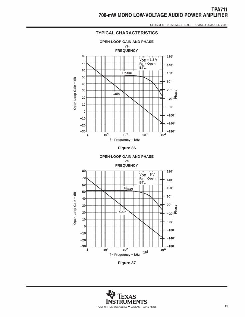
B1ÁÁÁÁÁÁÁÁÁÁÁÁÁÁÁÁÁÁUnity-gain bandwidth ÁÁÁÁÁ
ÁÁÁÁÁOpen Loop, ÁÁÁÁÁÁ
ÁÁÁÁÁÁSee Figure 36 ÁÁÁÁÁ
ÁÁÁÁÁÁÁÁÁÁÁ
ÁÁÁÁÁÁ
1.4ÁÁÁÁÁÁ
ÁÁÁÁÁÁ
MHz
ÁÁÁÁÁÁÁÁ
ÁÁÁÁÁÁÁÁÁÁÁÁÁÁÁÁÁÁSupply ripple rejection ratio
ÁÁÁÁÁÁÁÁÁÁ
f = 1 kHz,See Figure 5
ÁÁÁÁÁÁÁÁÁÁÁÁ
CB = 1 µF, ÁÁÁÁÁÁÁÁÁÁ
BTL mode, ÁÁÁÁÁÁ
ÁÁÁÁÁÁ
79ÁÁÁÁÁÁ
ÁÁÁÁÁÁdBÁÁÁÁ
ÁÁÁÁÁÁÁÁ
ÁÁÁÁÁÁÁÁÁÁÁÁÁÁÁÁÁÁÁÁÁÁÁÁÁÁÁ
Supply ripple rejection ratio ÁÁÁÁÁÁÁÁÁÁÁÁÁÁÁ
f = 1 kHz,See Figure 3
ÁÁÁÁÁÁÁÁÁÁÁÁÁÁÁÁÁÁ
CB = 1 µF,ÁÁÁÁÁÁÁÁÁÁÁÁÁÁÁ
SE mode,ÁÁÁÁÁÁÁÁÁ
ÁÁÁÁÁÁÁÁÁ
70
ÁÁÁÁÁÁÁÁÁ
ÁÁÁÁÁÁÁÁÁ
dB
ÁÁÁÁÁÁÁÁ
VnÁÁÁÁÁÁÁÁÁÁÁÁÁÁÁÁÁÁNoise output voltage ÁÁÁÁÁ
ÁÁÁÁÁGain = 1, ÁÁÁÁÁÁ
ÁÁÁÁÁÁCB = 0.1 µF, ÁÁÁÁÁ
ÁÁÁÁÁSee Figure 42ÁÁÁ
ÁÁÁÁÁÁÁÁÁ
17ÁÁÁÁÁÁ
ÁÁÁÁÁÁ
µV(rms)
NOTE 1: Output power is measured at the output terminals of the device at f = 1 kHz.
SLOS230D − NOVEMBER 1998 − REVISED OCTOBER 2002
4 POST OFFICE BOX 655303 • DALLAS, TEXAS 75265
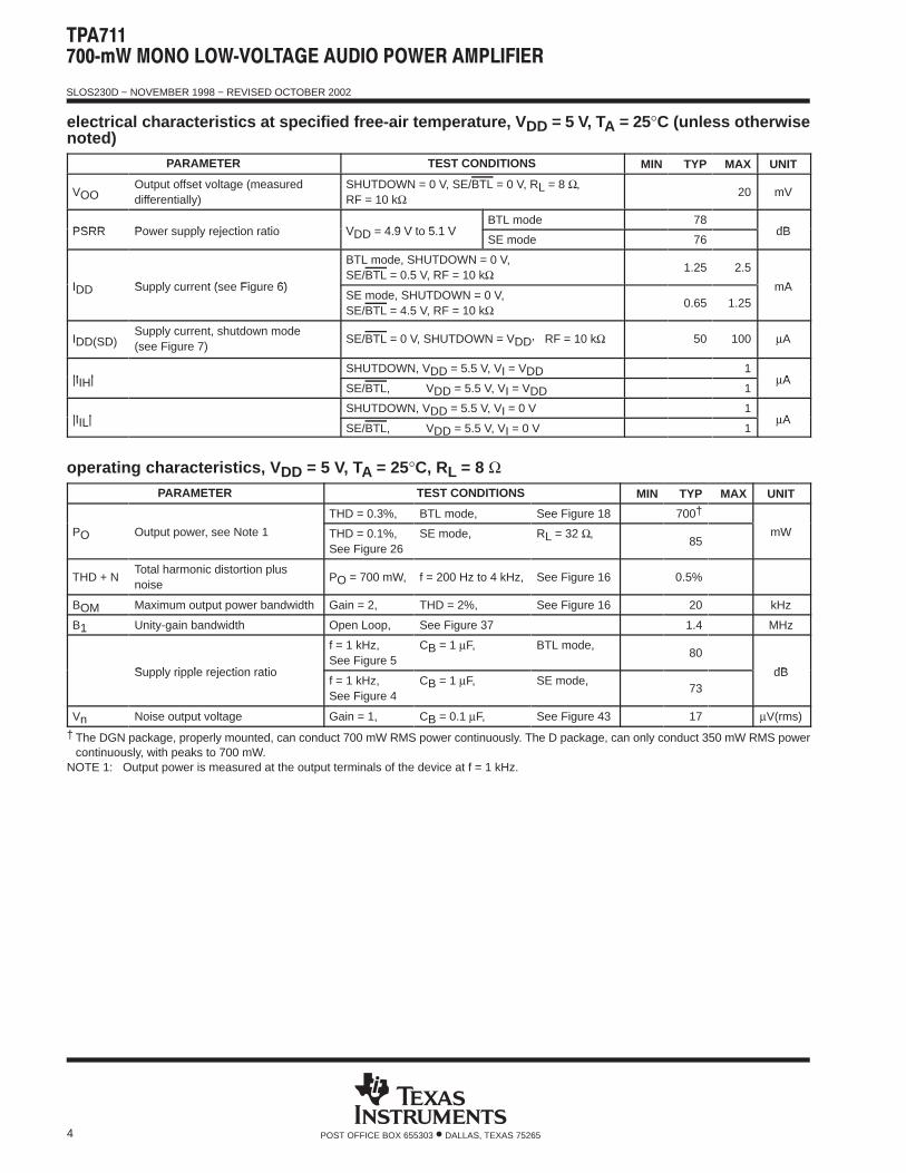
electrical characteristics at specified free-air temperature, V DD = 5 V, TA = 25°C (unless otherwisenoted)
PARAMETER TEST CONDITIONS MIN TYP MAX UNITÁÁÁÁÁÁÁÁÁÁÁÁ
VOO
ÁÁÁÁÁÁÁÁÁÁÁÁÁÁÁÁÁÁÁÁÁÁÁÁÁÁÁÁÁÁ
Output offset voltage (measureddifferentially)
ÁÁÁÁÁÁÁÁÁÁÁÁÁÁÁÁÁÁÁÁÁÁÁÁÁÁÁÁÁÁÁÁÁÁÁÁÁÁÁÁÁÁ
SHUTDOWN = 0 V, SE/BTL = 0 V, RL = 8 Ω, RF = 10 kΩ
ÁÁÁÁÁÁÁÁÁ
ÁÁÁÁÁÁÁÁÁ
ÁÁÁÁÁÁÁÁÁ
20ÁÁÁÁÁÁÁÁÁ
mV
ÁÁÁÁÁÁÁÁ
PSRRÁÁÁÁÁÁÁÁÁÁÁÁÁÁÁÁÁÁÁÁ
Power supply rejection ratioÁÁÁÁÁÁÁÁÁÁÁÁÁÁÁÁ
VDD = 4.9 V to 5.1 VÁÁÁÁÁÁÁÁÁÁÁÁÁÁ
BTL mode ÁÁÁÁÁÁ
ÁÁÁÁÁÁ
78ÁÁÁÁÁÁ
ÁÁÁÁÁÁ
dBÁÁÁÁ
PSRRÁÁÁÁÁÁÁÁÁÁ
Power supply rejection ratioÁÁÁÁÁÁÁÁ
VDD = 4.9 V to 5.1 VÁÁÁÁÁÁÁSE mode ÁÁÁÁÁÁ76ÁÁÁÁÁÁ
dBÁÁÁÁÁÁÁÁÁÁÁÁIDD
ÁÁÁÁÁÁÁÁÁÁÁÁÁÁÁÁÁÁÁÁÁÁÁÁÁÁÁÁÁÁSupply current (see Figure 6)
ÁÁÁÁÁÁÁÁÁÁÁÁÁÁÁÁÁÁÁÁÁÁÁÁÁÁÁÁÁÁÁÁÁÁÁÁÁÁÁÁÁÁ
BTL mode, SHUTDOWN = 0 V,SE/BTL = 0.5 V, RF = 10 kΩ
ÁÁÁÁÁÁÁÁÁ
ÁÁÁÁÁÁÁÁÁ
1.25
ÁÁÁÁÁÁÁÁÁ
2.5
ÁÁÁÁÁÁÁÁÁmAÁÁÁÁ
ÁÁÁÁÁÁÁÁ
IDD ÁÁÁÁÁÁÁÁÁÁÁÁÁÁÁÁÁÁÁÁÁÁÁÁÁÁÁÁÁÁ
Supply current (see Figure 6) ÁÁÁÁÁÁÁÁÁÁÁÁÁÁÁÁÁÁÁÁÁÁÁÁÁÁÁÁÁÁÁÁÁÁÁÁÁÁÁÁÁÁ
SE mode, SHUTDOWN = 0 V,SE/BTL = 4.5 V, RF = 10 kΩ
ÁÁÁÁÁÁÁÁÁ
ÁÁÁÁÁÁÁÁÁ
0.65ÁÁÁÁÁÁÁÁÁ
1.25ÁÁÁÁÁÁÁÁÁ
mA
ÁÁÁÁÁÁÁÁ
IDD(SD)ÁÁÁÁÁÁÁÁÁÁÁÁÁÁÁÁÁÁÁÁ
Supply current, shutdown mode(see Figure 7)
ÁÁÁÁÁÁÁÁÁÁÁÁÁÁÁÁÁÁÁÁÁÁÁÁÁÁÁÁ
SE/BTL = 0 V, SHUTDOWN = VDD, RF = 10 kΩ ÁÁÁÁÁÁ
ÁÁÁÁÁÁ
50ÁÁÁÁÁÁ
100ÁÁÁÁÁÁ
µA
ÁÁÁÁÁÁÁÁ|IIH|
ÁÁÁÁÁÁÁÁÁÁÁÁÁÁÁÁÁÁÁÁ
ÁÁÁÁÁÁÁÁÁÁÁÁÁÁÁÁÁÁÁÁÁÁÁÁÁÁÁÁ
SHUTDOWN, VDD = 5.5 V, VI = VDDÁÁÁÁÁÁ
ÁÁÁÁÁÁ
ÁÁÁÁÁÁ
1ÁÁÁÁÁÁAÁÁÁÁ
ÁÁÁÁ|IIH| ÁÁÁÁÁÁÁÁÁÁÁÁÁÁÁÁÁÁÁÁ
ÁÁÁÁÁÁÁÁÁÁÁÁÁÁÁÁÁÁÁÁÁÁÁÁÁÁÁÁ
SE/BTL, VDD = 5.5 V, VI = VDDÁÁÁÁÁÁ
ÁÁÁÁÁÁ
ÁÁÁÁÁÁ
1ÁÁÁÁÁÁ
µA
ÁÁÁÁÁÁÁÁ|IIL|
ÁÁÁÁÁÁÁÁÁÁÁÁÁÁÁÁÁÁÁÁ
ÁÁÁÁÁÁÁÁÁÁÁÁÁÁÁÁÁÁÁÁÁÁÁÁÁÁÁÁ
SHUTDOWN, VDD = 5.5 V, VI = 0 V ÁÁÁÁÁÁ
ÁÁÁÁÁÁ
ÁÁÁÁÁÁ
1ÁÁÁÁÁÁAÁÁÁÁ
ÁÁÁÁ
|IIL| ÁÁÁÁÁÁÁÁÁÁÁÁÁÁÁÁÁÁÁÁ
ÁÁÁÁÁÁÁÁÁÁÁÁÁÁÁÁÁÁÁÁÁÁÁÁÁÁÁÁ
SE/BTL, VDD = 5.5 V, VI = 0 V ÁÁÁÁÁÁ
ÁÁÁÁÁÁ
ÁÁÁÁÁÁ
1ÁÁÁÁÁÁ
µA
operating characteristics, V DD = 5 V, TA = 25°C, RL = 8 ΩPARAMETER TEST CONDITIONS MIN TYP MAX UNIT
ÁÁÁÁÁÁÁÁÁÁÁÁÁÁÁÁÁÁÁTHD = 0.3%, ÁÁÁÁÁÁBTL mode, ÁÁÁÁÁSee Figure 18ÁÁÁÁÁÁ700†ÁÁÁÁÁÁÁÁÁÁÁÁÁÁÁÁÁÁ
POÁÁÁÁÁÁÁÁÁÁÁÁÁÁÁÁÁÁÁÁÁÁÁÁÁÁÁÁÁÁ
Output power, see Note 1ÁÁÁÁÁÁÁÁÁÁÁÁÁÁÁ
THD = 0.1%,See Figure 26
ÁÁÁÁÁÁÁÁÁÁÁÁÁÁÁÁÁÁ
SE mode,ÁÁÁÁÁÁÁÁÁÁÁÁÁÁÁ
RL = 32 Ω,ÁÁÁÁÁÁÁÁÁ
ÁÁÁÁÁÁÁÁÁ
85
ÁÁÁÁÁÁÁÁÁ
ÁÁÁÁÁÁÁÁÁ
mW
ÁÁÁÁÁÁÁÁÁÁÁÁ
THD + NÁÁÁÁÁÁÁÁÁÁÁÁÁÁÁÁÁÁÁÁÁÁÁÁÁÁÁÁÁÁ
Total harmonic distortion plusnoise
ÁÁÁÁÁÁÁÁÁÁÁÁÁÁÁ
PO = 700 mW,ÁÁÁÁÁÁÁÁÁÁÁÁÁÁÁÁÁÁ
f = 200 Hz to 4 kHz,ÁÁÁÁÁÁÁÁÁÁÁÁÁÁÁ
See Figure 16ÁÁÁÁÁÁÁÁÁ
ÁÁÁÁÁÁÁÁÁ
0.5%ÁÁÁÁÁÁÁÁÁ
ÁÁÁÁÁÁÁÁÁÁÁÁÁBOM ÁÁÁÁÁÁÁÁÁÁMaximum output power bandwidthÁÁÁÁÁGain = 2, ÁÁÁÁÁÁTHD = 2%, ÁÁÁÁÁSee Figure 16ÁÁÁÁÁÁ20ÁÁÁÁÁÁkHzÁÁÁÁ
ÁÁÁÁB1
ÁÁÁÁÁÁÁÁÁÁÁÁÁÁÁÁÁÁÁÁUnity-gain bandwidth
ÁÁÁÁÁÁÁÁÁÁOpen Loop,
ÁÁÁÁÁÁÁÁÁÁÁÁSee Figure 37
ÁÁÁÁÁÁÁÁÁÁ
ÁÁÁÁÁÁ
ÁÁÁÁÁÁ1.4
ÁÁÁÁÁÁ
ÁÁÁÁÁÁMHzÁÁÁÁ
ÁÁÁÁÁÁÁÁ
ÁÁÁÁÁÁÁÁÁÁÁÁÁÁÁÁÁÁÁÁÁÁÁÁÁÁÁÁÁÁSupply ripple rejection ratio
ÁÁÁÁÁÁÁÁÁÁÁÁÁÁÁ
f = 1 kHz,See Figure 5
ÁÁÁÁÁÁÁÁÁÁÁÁÁÁÁÁÁÁ
CB = 1 µF,ÁÁÁÁÁÁÁÁÁÁÁÁÁÁÁ
BTL mode,ÁÁÁÁÁÁÁÁÁ
ÁÁÁÁÁÁÁÁÁ
80
ÁÁÁÁÁÁÁÁÁ
ÁÁÁÁÁÁÁÁÁdBÁÁÁÁ
ÁÁÁÁÁÁÁÁ
ÁÁÁÁÁÁÁÁÁÁÁÁÁÁÁÁÁÁÁÁÁÁÁÁÁÁÁÁÁÁ
Supply ripple rejection ratio ÁÁÁÁÁÁÁÁÁÁÁÁÁÁÁ
f = 1 kHz,See Figure 4
ÁÁÁÁÁÁÁÁÁÁÁÁÁÁÁÁÁÁ
CB = 1 µF, ÁÁÁÁÁÁÁÁÁÁÁÁÁÁÁ
SE mode, ÁÁÁÁÁÁÁÁÁ
ÁÁÁÁÁÁÁÁÁ
73ÁÁÁÁÁÁÁÁÁ
ÁÁÁÁÁÁÁÁÁ
dB
ÁÁÁÁVn ÁÁÁÁÁÁÁÁÁÁNoise output voltage ÁÁÁÁÁGain = 1, ÁÁÁÁÁÁCB = 0.1 µF, ÁÁÁÁÁSee Figure 43ÁÁÁÁÁÁ17ÁÁÁÁÁÁµV(rms)
† The DGN package, properly mounted, can conduct 700 mW RMS power continuously. The D package, can only conduct 350 mW RMS powercontinuously, with peaks to 700 mW.
NOTE 1: Output power is measured at the output terminals of the device at f = 1 kHz.
SLOS230D − NOVEMBER 1998 − REVISED OCTOBER 2002
5POST OFFICE BOX 655303 • DALLAS, TEXAS 75265
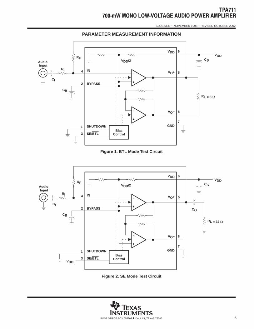
PARAMETER MEASUREMENT INFORMATION
Audio Input
BiasControl
VDD6
5
7
VO+
VDD
3
1
2
4
BYPASS
IN
SE/BTL
VDD/2
CI
RI
CS
CB
RF
SHUTDOWN
VO− 8
RL = 8 Ω
GND
−
+
−
+
Figure 1. BTL Mode Test Circuit
Audio Input
BiasControl
VDD
6
5
7
VO+
VDD
3
1
2
4
BYPASS
IN
SE/BTL
VDD/2
CI
RI
CS
CB
RF
SHUTDOWN
VO− 8
RL = 32 Ω
GND
CO
VDD
−
+
−
+
Figure 2. SE Mode Test Circuit
SLOS230D − NOVEMBER 1998 − REVISED OCTOBER 2002
6 POST OFFICE BOX 655303 • DALLAS, TEXAS 75265
TYPICAL CHARACTERISTICS
Table of GraphsFIGURE
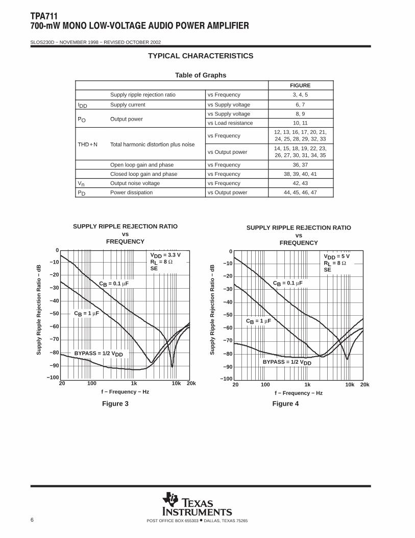
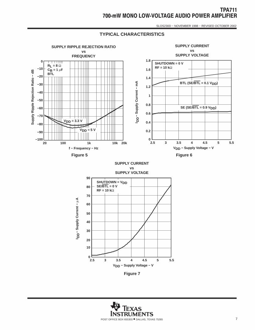
Supply ripple rejection ratio vs Frequency 3, 4, 5
IDD Supply current vs Supply voltage 6, 7
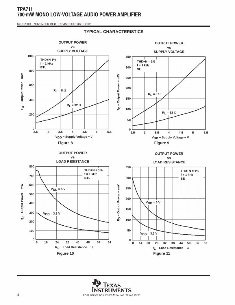
PO Output powervs Supply voltage 8, 9
PO Output powervs Load resistance 10, 11
THD+N Total harmonic distortion plus noise
vs Frequency12, 13, 16, 17, 20, 21,24, 25, 28, 29, 32, 33
THD+N Total harmonic distortion plus noisevs Output power
14, 15, 18, 19, 22, 23,26, 27, 30, 31, 34, 35
Open loop gain and phase vs Frequency 36, 37
Closed loop gain and phase vs Frequency 38, 39, 40, 41
Vn Output noise voltage vs Frequency 42, 43
PD Power dissipation vs Output power 44, 45, 46, 47
Figure 3
−50
−60
−80
−10020 100 1k
−30
−20
f − Frequency − Hz
SUPPLY RIPPLE REJECTION RATIOvs
FREQUENCY0
10k 20k
−10
−40
−70
−90
BYPASS = 1/2 VDD
CB = 0.1 µF
VDD = 3.3 VRL = 8 ΩSE
CB = 1 µF
Sup
ply
Rip
ple
Rej
ectio
n R
atio
− d
B
Figure 4
−50
−60
−80
−10020 100 1k
−30
−20
f − Frequency − Hz
SUPPLY RIPPLE REJECTION RATIOvs
FREQUENCY0
10k 20k
−10
−40
−70
−90BYPASS = 1/2 VDD
CB = 0.1 µF
VDD = 5 VRL = 8 ΩSE
CB = 1 µF
Sup
ply
Rip
ple
Rej
ectio
n R
atio
− d
B
SLOS230D − NOVEMBER 1998 − REVISED OCTOBER 2002
7POST OFFICE BOX 655303 • DALLAS, TEXAS 75265
TYPICAL CHARACTERISTICS
Figure 5
−50
−60
−80
−10020 100 1k
−30
−20
f − Frequency − Hz
SUPPLY RIPPLE REJECTION RATIOvs
FREQUENCY0
10k 20k
−10
−40
−70
−90VDD = 5 V
VDD = 3.3 V
RL = 8 ΩCB = 1 µFBTL
Sup
ply
Rip
ple
Rej
ectio
n R
atio
− d
B
Figure 6
VDD − Supply Voltage − V
SUPPLY CURRENTvs
SUPPLY VOLTAGE1.8
1.4
0.4
0
1.6
1.2
0.2
3 3.5 5.54.5
I DD
− S
uppl
y C
urre
nt −
mA
42.5 5
0.8
0.6
1
BTL (SE/BTL = 0.1 VDD)
SHUTDOWN = 0 VRF = 10 kΩ
SE (SE/BTL = 0.9 VDD)
2.5
VDD − Supply Voltage − V
SUPPLY CURRENTvs
SUPPLY VOLTAGE
20
10
03 43.5 4.5
60
5
30
SHUTDOWN = VDDSE/BTL = 0 VRF = 10 kΩ
40
50
5.5
I DD
− S
uppl
y C
urre
nt −
Aµ
70
80
90
Figure 7
SLOS230D − NOVEMBER 1998 − REVISED OCTOBER 2002
8 POST OFFICE BOX 655303 • DALLAS, TEXAS 75265
TYPICAL CHARACTERISTICS
Figure 8
VDD − Supply Voltage − V
OUTPUT POWERvs
SUPPLY VOLTAGE
600
400
200
02.5 3.53 4 5.5
1000
P
4.5 5
O−
Out
put P
ower
− m
W
800
THD+N 1%f = 1 kHzBTL
RL = 32 Ω
RL = 8 Ω
Figure 9
VDD − Supply Voltage − V
OUTPUT POWERvs
SUPPLY VOLTAGE
150
100
50
03 43.5 4.5
350
P
5
O−
Out
put P
ower
− m
W
200
THD+N = 1%f = 1 kHzSE
RL = 32 Ω
RL = 8 Ω
250
300
5.52.5
Figure 10
RL − Load Resistance − Ω
OUTPUT POWERvs
LOAD RESISTANCE
300
200
100
016 3224 40 64
800
8
P
48 56
O−
Out
put P
ower
− m
W
400
THD+N = 1%f = 1 kHzBTL
VDD = 5 V
500
600
VDD = 3.3 V
700
Figure 11
RL − Load Resistance − Ω
OUTPUT POWERvs
LOAD RESISTANCE
14 2620 32 508 38 44
THD+N = 1%f = 1 kHzSE
VDD = 5 V
VDD = 3.3 V
56 62
150
100
50
0
350
P O−
Out
put P
ower
− m
W
200
250
300
SLOS230D − NOVEMBER 1998 − REVISED OCTOBER 2002
9POST OFFICE BOX 655303 • DALLAS, TEXAS 75265
TYPICAL CHARACTERISTICS
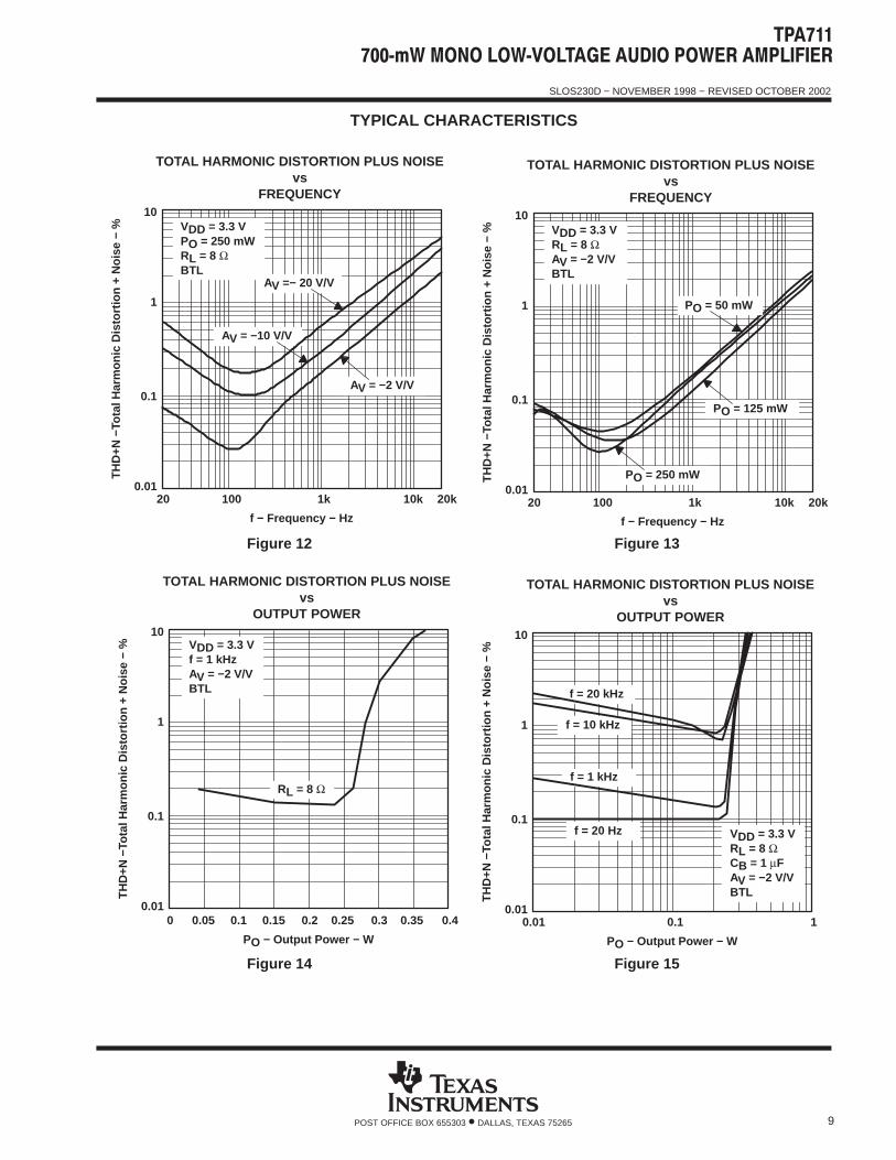
Figure 12
f − Frequency − Hz
TH
D+N
−To
tal H
arm
onic
Dis
tort
ion
+ N
oise
− %
TOTAL HARMONIC DISTORTION PLUS NOISEvs
FREQUENCY
AV = −2 V/V
VDD = 3.3 VPO = 250 mWRL = 8 ΩBTL
20 1k 10k
1
0.01
10
0.1
20k100
AV =− 20 V/V
AV = −10 V/V
Figure 13
f − Frequency − Hz
TH
D+N
−To
tal H
arm
onic
Dis
tort
ion
+ N
oise
− %
TOTAL HARMONIC DISTORTION PLUS NOISEvs
FREQUENCY
PO = 125 mW
VDD = 3.3 VRL = 8 ΩAV = −2 V/VBTL
20 1k 10k
1
0.01
10
0.1
20k100
PO = 50 mW
PO = 250 mW
Figure 14
PO − Output Power − W
TH
D+N
−To
tal H
arm
onic
Dis
tort
ion
+ N
oise
− %
TOTAL HARMONIC DISTORTION PLUS NOISEvs
OUTPUT POWER
0 0.15 0.4
1
0.01
10
0.1
0.2 0.25 0.3 0.35
VDD = 3.3 Vf = 1 kHzAV = −2 V/VBTL
0.05 0.1
RL = 8 Ω
Figure 15
PO − Output Power − W
TH
D+N
−To
tal H
arm
onic
Dis
tort
ion
+ N
oise
− %
TOTAL HARMONIC DISTORTION PLUS NOISEvs
OUTPUT POWER
f = 20 kHz
VDD = 3.3 VRL = 8 ΩCB = 1 µFAV = −2 V/VBTL
0.01 0.1 1
1
0.01
10
0.1
f = 1 kHz
f = 10 kHz
f = 20 Hz
SLOS230D − NOVEMBER 1998 − REVISED OCTOBER 2002
10 POST OFFICE BOX 655303 • DALLAS, TEXAS 75265
TYPICAL CHARACTERISTICS
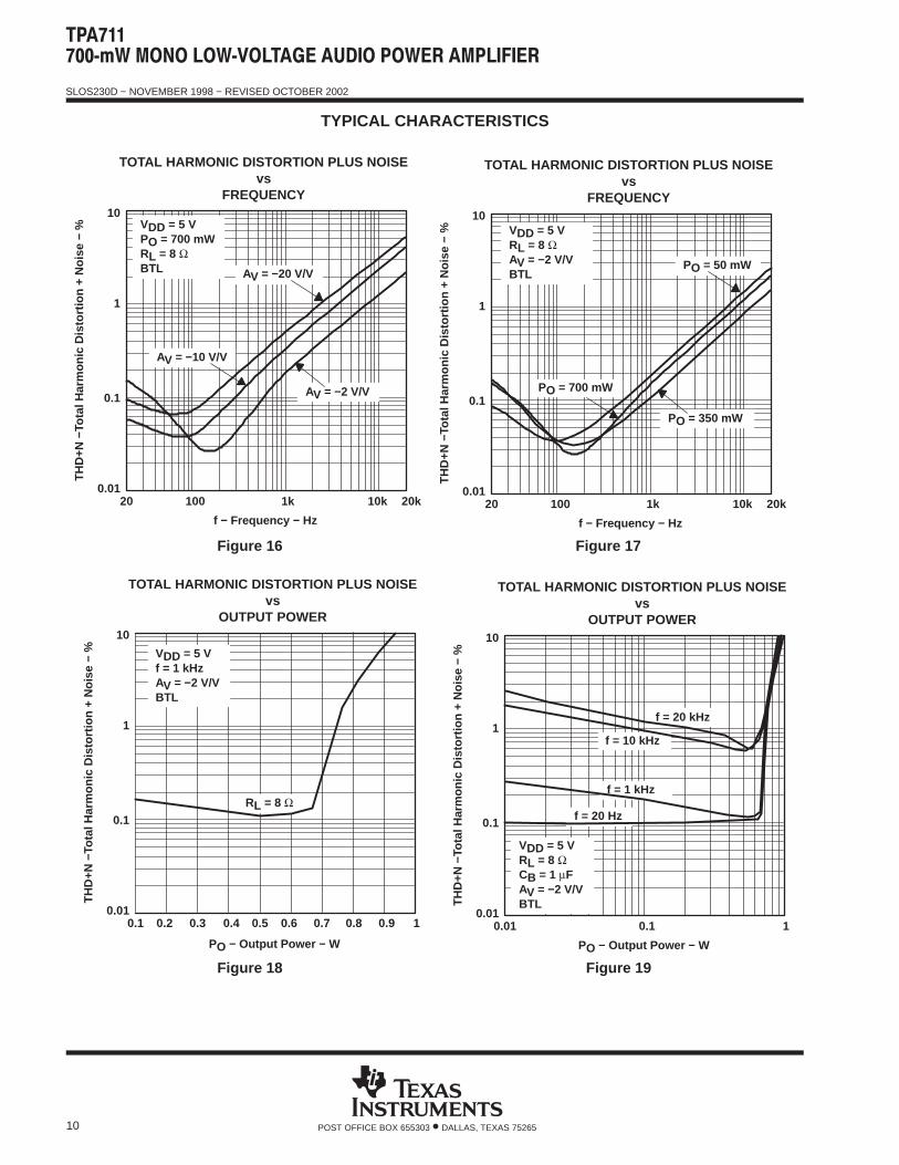
Figure 16
f − Frequency − Hz
TH
D+N
−To
tal H
arm
onic
Dis
tort
ion
+ N
oise
− %
TOTAL HARMONIC DISTORTION PLUS NOISEvs
FREQUENCY
AV = −2 V/V
VDD = 5 VPO = 700 mWRL = 8 ΩBTL
20 1k 10k
1
0.01
10
0.1
20k100
AV = −20 V/V
AV = −10 V/V
Figure 17
f − Frequency − Hz
TH
D+N
−To
tal H
arm
onic
Dis
tort
ion
+ N
oise
− %
TOTAL HARMONIC DISTORTION PLUS NOISEvs
FREQUENCY
PO = 700 mW
VDD = 5 VRL = 8 ΩAV = −2 V/VBTL
20 1k 10k
1
0.01
10
0.1
20k100
PO = 50 mW
PO = 350 mW
Figure 18
PO − Output Power − W
0.1 0.2 10.4 0.5 0.7 0.8
TH
D+N
−To
tal H
arm
onic
Dis
tort
ion
+ N
oise
− %
TOTAL HARMONIC DISTORTION PLUS NOISEvs
OUTPUT POWER
RL = 8 Ω
VDD = 5 Vf = 1 kHzAV = −2 V/VBTL
1
0.01
10
0.1
0.3 0.6 0.9
Figure 19
PO − Output Power − W
TH
D+N
−To
tal H
arm
onic
Dis
tort
ion
+ N
oise
− %
TOTAL HARMONIC DISTORTION PLUS NOISEvs
OUTPUT POWER
f = 20 Hz
VDD = 5 VRL = 8 ΩCB = 1 µFAV = −2 V/VBTL
0.01 0.1 1
1
0.01
10
0.1
f = 1 kHz
f = 10 kHz
f = 20 kHz
SLOS230D − NOVEMBER 1998 − REVISED OCTOBER 2002
11POST OFFICE BOX 655303 • DALLAS, TEXAS 75265
TYPICAL CHARACTERISTICS
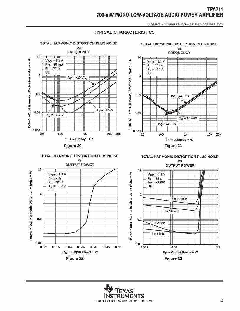
Figure 20
f − Frequency − Hz
TH
D+N
−To
tal H
arm
onic
Dis
tort
ion
+ N
oise
− %
TOTAL HARMONIC DISTORTION PLUS NOISEvs
FREQUENCY
AV = −10 V/V
VDD = 3.3 VPO = 30 mWRL = 32 ΩSE
20 1k 10k
0.1
0.001
10
0.01
20k100
AV = −1 V/V
1
AV = −5 V/V
Figure 21
f − Frequency − Hz
TH
D+N
−To
tal H
arm
onic
Dis
tort
ion
+ N
oise
− %
TOTAL HARMONIC DISTORTION PLUS NOISEvs
FREQUENCY
VDD = 3.3 VRL = 32 ΩAV = −1 V/VSE
20 1k 10k
0.1
0.001
10
0.01
20k100
PO = 10 mW
PO = 15 mW
1
PO = 30 mW
Figure 22
TH
D+N
−To
tal H
arm
onic
Dis
tort
ion
+ N
oise
− %
TOTAL HARMONIC DISTORTION PLUS NOISEvs
OUTPUT POWER
VDD = 3.3 Vf = 1 kHzRL = 32 ΩAV = −1 V/VSE
1
0.01
10
0.1
PO − Output Power − W
0.02 0.025 0.050.03 0.035 0.04 0.045
Figure 23
PO − Output Power − W
TH
D+N
−To
tal H
arm
onic
Dis
tort
ion
+ N
oise
− %
TOTAL HARMONIC DISTORTION PLUS NOISEvs
OUTPUT POWER
f = 20 Hz
1
0.01
10
0.1
f = 1 kHz
f = 10 kHz
f = 20 kHz
0.002 0.10.01
VDD = 3.3 VRL = 32 ΩAV = −1 V/VSE
SLOS230D − NOVEMBER 1998 − REVISED OCTOBER 2002
12 POST OFFICE BOX 655303 • DALLAS, TEXAS 75265
TYPICAL CHARACTERISTICS
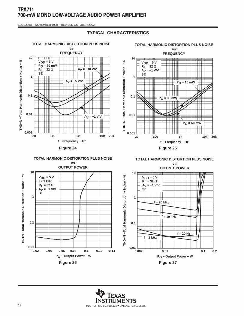
Figure 24
f − Frequency − Hz
TH
D+N
−To
tal H
arm
onic
Dis
tort
ion
+ N
oise
− %
TOTAL HARMONIC DISTORTION PLUS NOISEvs
FREQUENCY
AV = −10 V/V
VDD = 5 VPO = 60 mWRL = 32 ΩSE
20 1k 10k
0.1
0.001
10
0.01
20k100
AV = −1 V/V
1AV = −5 V/V
Figure 25
f − Frequency − Hz
TH
D+N
−To
tal H
arm
onic
Dis
tort
ion
+ N
oise
− %
TOTAL HARMONIC DISTORTION PLUS NOISEvs
FREQUENCY
VDD = 5 VRL = 32 ΩAV = −1 V/VSE
20 1k 10k
0.1
0.001
10
0.01
20k100
PO = 15 mW
PO = 60 mW
1
PO = 30 mW
Figure 26
TH
D+N
−To
tal H
arm
onic
Dis
tort
ion
+ N
oise
− %
TOTAL HARMONIC DISTORTION PLUS NOISEvs
OUTPUT POWER
VDD = 5 Vf = 1 kHzRL = 32 ΩAV = −1 V/VSE
1
0.01
10
0.1
PO − Output Power − W
0.02 0.04 0.140.06 0.08 0.1 0.12
Figure 27
PO − Output Power − W
TH
D+N
−To
tal H
arm
onic
Dis
tort
ion
+ N
oise
− %
TOTAL HARMONIC DISTORTION PLUS NOISEvs
OUTPUT POWER
f = 20 Hz
VDD = 5 VRL = 32 ΩAV = −1 V/VSE
1
0.01
10
0.1
f = 1 kHz
f = 10 kHz
f = 20 kHz
0.002 0.1 0.20.01
SLOS230D − NOVEMBER 1998 − REVISED OCTOBER 2002
13POST OFFICE BOX 655303 • DALLAS, TEXAS 75265
TYPICAL CHARACTERISTICS
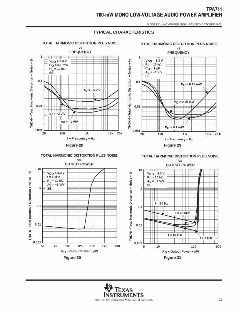
Figure 28
f − Frequency − Hz
TH
D+N
−To
tal H
arm
onic
Dis
tort
ion
+ N
oise
− %
TOTAL HARMONIC DISTORTION PLUS NOISEvs
FREQUENCY
20 1k 10k
0.1
0.001
1
20k100
0.01
VDD = 3.3 VPO = 0.1 mWRL = 10 kΩSE
AV = −5 V/V
AV = −2 V/V
AV = −1 V/V
Figure 29
f − Frequency − Hz
TH
D+N
−To
tal H
arm
onic
Dis
tort
ion
+ N
oise
− %
TOTAL HARMONIC DISTORTION PLUS NOISEvs
FREQUENCY
20 1 k 10 k
0.01
0.001
1
20 k100
0.1
VDD = 3.3 VRL = 10 kΩCB = 1 µFAV = −1 V/VSE
PO = 0.13 mW
PO = 0.05 mW
PO = 0.1 mW
Figure 30
TH
D+N
−To
tal H
arm
onic
Dis
tort
ion
+ N
oise
− %
TOTAL HARMONIC DISTORTION PLUS NOISEvs
OUTPUT POWER
VDD = 3.3 Vf = 1 kHzRL = 10 kΩAV = −1 V/VSE
0.1
0.001
10
0.01
1
PO − Output Power − µW
50 75 200100 125 150 175
Figure 31
PO − Output Power − µW
TH
D+N
−To
tal H
arm
onic
Dis
tort
ion
+ N
oise
− %
TOTAL HARMONIC DISTORTION PLUS NOISEvs
OUTPUT POWER
f = 20 Hz
VDD = 3.3 VRL = 10 kΩAV = −1 V/VSE
f = 1 kHzf = 10 kHz
f = 20 kHz
5 100 500
0.1
0.001
10
0.01
1
10
SLOS230D − NOVEMBER 1998 − REVISED OCTOBER 2002
14 POST OFFICE BOX 655303 • DALLAS, TEXAS 75265
TYPICAL CHARACTERISTICS
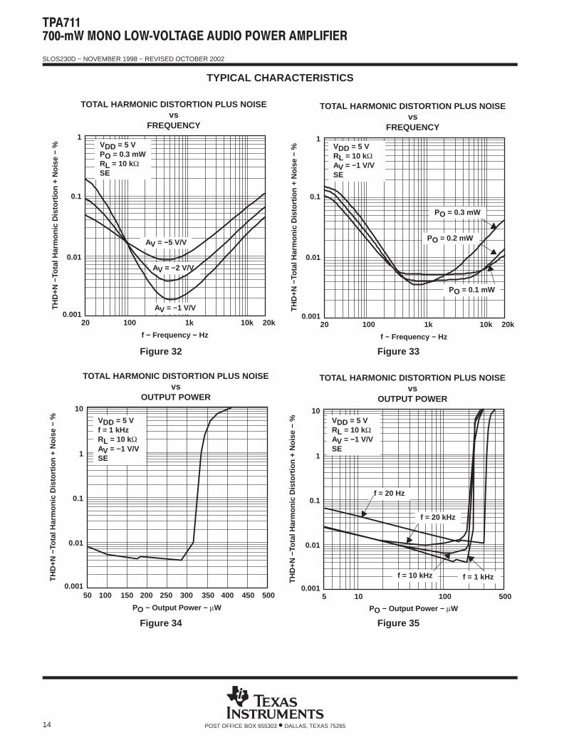
Figure 32
f − Frequency − Hz
TH
D+N
−To
tal H
arm
onic
Dis
tort
ion
+ N
oise
− %
TOTAL HARMONIC DISTORTION PLUS NOISEvs
FREQUENCY
VDD = 5 VPO = 0.3 mWRL = 10 kΩSE
20 1k 10k
0.01
0.001
1
20k100
AV = −1 V/V
AV = −2 V/V
AV = −5 V/V
0.1
Figure 33
f − Frequency − Hz
TH
D+N
−To
tal H
arm
onic
Dis
tort
ion
+ N
oise
− %
TOTAL HARMONIC DISTORTION PLUS NOISEvs
FREQUENCY
20 1k 10k
0.01
0.001
1
20k100
0.1
VDD = 5 VRL = 10 kΩAV = −1 V/VSE
PO = 0.1 mW
PO = 0.3 mW
PO = 0.2 mW
Figure 34
TH
D+N
−To
tal H
arm
onic
Dis
tort
ion
+ N
oise
− %
TOTAL HARMONIC DISTORTION PLUS NOISEvs
OUTPUT POWER
VDD = 5 Vf = 1 kHzRL = 10 kΩAV = −1 V/VSE
0.1
0.001
10
0.01
1
PO − Output Power − µW
50 100 500150 200 250 300 350 400 450
Figure 35
PO − Output Power − µW
TH
D+N
−To
tal H
arm
onic
Dis
tort
ion
+ N
oise
− %
TOTAL HARMONIC DISTORTION PLUS NOISEvs
OUTPUT POWER
f = 20 Hz
VDD = 5 VRL = 10 kΩAV = −1 V/VSE
f = 10 kHz
5 100 500
0.1
0.001
10
0.01
1
10
f = 1 kHz
f = 20 kHz
SLOS230D − NOVEMBER 1998 − REVISED OCTOBER 2002
15POST OFFICE BOX 655303 • DALLAS, TEXAS 75265
TYPICAL CHARACTERISTICS
10
0
−20
−30
20
30
f − Frequency − kHz
80
−10
180°
−180°
Phase
60°
−60°
OPEN-LOOP GAIN AND PHASEvs
FREQUENCY
Ope
n-Lo
op G
ain
− dB
Pha
se
1 101 102 103 104
50
40
60
70140°
100°
20°
−20°
−100°
−140°
VDD = 3.3 VRL = OpenBTL
Gain
Figure 36
10
0
−20
−301
20
30
f − Frequency − kHz
80
−10
Gain
Phase
OPEN-LOOP GAIN AND PHASEvs
FREQUENCY
Ope
n-Lo
op G
ain
− dB
101 102103 104
50
40
60
70VDD = 5 VRL = OpenBTL
180°
−180°
60°
−60°
Pha
se
140°
100°
20°
−20°
−100°
−140°
Figure 37
SLOS230D − NOVEMBER 1998 − REVISED OCTOBER 2002
16 POST OFFICE BOX 655303 • DALLAS, TEXAS 75265
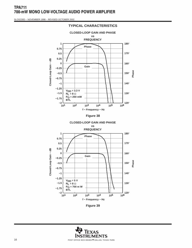
TYPICAL CHARACTERISTICS
CLOSED-LOOP GAIN AND PHASEvs
FREQUENCY
−0.5
−1
−1.5
−2
f − Frequency − Hz
−0.25
−0.75
−1.25
−1.75
0
0.5C
lose
d-Lo
op G
ain
− dB
0.25
0.75
130°
120°
140°
Pha
se
150°
160°
VDD = 3.3 VRL = 8 ΩPO = 250 mWBTL
1
170°
180°
Gain
Phase
101 102 103 104 105 106
Figure 38
CLOSED-LOOP GAIN AND PHASEvs
FREQUENCY
−0.5
−1
−1.5
−2
f − Frequency − Hz
−0.25
−0.75
−1.25
−1.75
0
0.5
Clo
sed-
Loop
Gai
n −
dB
0.25
0.75
130°
120°
140°
Pha
se
150°
160°
VDD = 5 VRL = 8 ΩPO = 700 m WBTL
1
170°
180°
Gain
Phase
101 102 103 104 105 106
Figure 39
SLOS230D − NOVEMBER 1998 − REVISED OCTOBER 2002
17POST OFFICE BOX 655303 • DALLAS, TEXAS 75265
TYPICAL CHARACTERISTICS
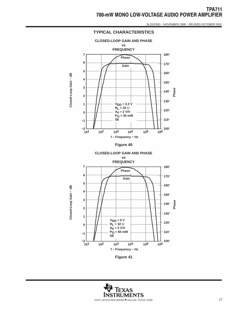
CLOSED-LOOP GAIN AND PHASEvs
FREQUENCY
3
1
−1
−2
f − Frequency − Hz
4
2
0
5
7
Clo
sed-
Loop
Gai
n −
dB
6
VDD = 3.3 VRL = 32 ΩAV = 2 V/VPO = 30 mWSE
Gain
Phase
110°
100°
120°
Pha
se
130°
140°
150°
180°
160°
170°
101 102 103 104 105 106
Figure 40
CLOSED-LOOP GAIN AND PHASEvs
FREQUENCY
4
2
0
−2
f − Frequency − Hz
5
3
1
−1
6
Clo
sed-
Loop
Gai
n −
dB
7
110°
100°
120°
Pha
se
130°
140°
VDD = 5 VRL = 32 ΩAV = 2 V/VPO = 60 mWSE
150°
180°
Gain
Phase
160°
170°
101 102 103 104 105 106
Figure 41
SLOS230D − NOVEMBER 1998 − REVISED OCTOBER 2002
18 POST OFFICE BOX 655303 • DALLAS, TEXAS 75265
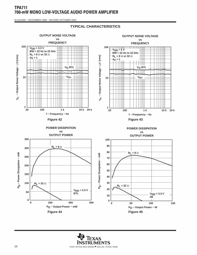
TYPICAL CHARACTERISTICS
Figure 42
− O
utpu
t Noi
se V
olta
ge −
VµV
n
f − Frequency − Hz
OUTPUT NOISE VOLTAGEvs
FREQUENCY
20 1 k 10 k
10
1
100
20 k100
VO BTL
VDD = 3.3 VBW = 22 Hz to 22 kHzRL = 8 Ω or 32 ΩAV = 1
VO+
(rm
s)
Figure 43
− O
utpu
t Noi
se V
olta
ge −
VµV
n
f − Frequency − Hz
OUTPUT NOISE VOLTAGEvs
FREQUENCY
20 1 k 10 k
10
1
100
20 k100
VDD = 5 VBW = 22 Hz to 22 kHzRL = 8 Ω or 32 ΩAV = 1
VO BTL
VO+
(rm
s)
Figure 44
PD − Output Power − mW
POWER DISSIPATIONvs
OUTPUT POWER
400 6000
150
100
50
0
350
PD
− P
ower
Dis
sipa
tion
− m
W
200
250
300
200
VDD = 3.3 VBTL
RL = 32 Ω
RL = 8 Ω
Figure 45
PD − Output Power − W
POWER DISSIPATIONvs
OUTPUT POWER
1500
30
20
10
0
70
PD
− P
ower
Dis
sipa
tion
− m
W
40
50
60
100
80
90
50 100
VDD = 3.3 VSE
RL = 32 Ω
RL = 8 Ω
SLOS230D − NOVEMBER 1998 − REVISED OCTOBER 2002
19POST OFFICE BOX 655303 • DALLAS, TEXAS 75265
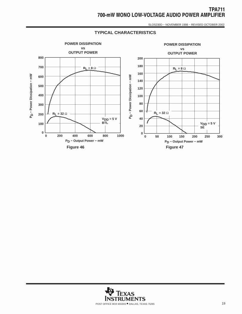
TYPICAL CHARACTERISTICS
Figure 46
PD − Output Power − mW
POWER DISSIPATIONvs
OUTPUT POWER
200 600400 8000 1000
400
300
100
0
800
PD
− P
ower
Dis
sipa
tion
− m
W
500
600
700
200VDD = 5 VBTL
RL = 32 Ω
RL = 8 Ω
Figure 47
PD − Output Power − mW
POWER DISSIPATIONvs
OUTPUT POWER
50 150100 2000 250 300
100
80
60
0
200
PD
− P
ower
Dis
sipa
tion
− m
W
120
140
160
20
40
180
VDD = 5 VSE
RL = 8 Ω
RL = 32 Ω
SLOS230D − NOVEMBER 1998 − REVISED OCTOBER 2002
20 POST OFFICE BOX 655303 • DALLAS, TEXAS 75265
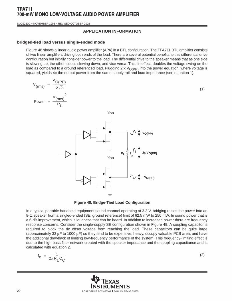
APPLICATION INFORMATION
bridged-tied load versus single-ended mode
Figure 48 shows a linear audio power amplifier (APA) in a BTL configuration. The TPA711 BTL amplifier consistsof two linear amplifiers driving both ends of the load. There are several potential benefits to this differential driveconfiguration but initially consider power to the load. The differential drive to the speaker means that as one sideis slewing up, the other side is slewing down, and vice versa. This, in effect, doubles the voltage swing on theload as compared to a ground referenced load. Plugging 2 × VO(PP) into the power equation, where voltage issquared, yields 4× the output power from the same supply rail and load impedance (see equation 1).
Power V(rms)
2
RL
(1)V(rms)
VO(PP)
2 2
RL 2x VO(PP)
VO(PP)
−VO(PP)
VDD
VDD
Figure 48. Bridge-Tied Load Configuration
In a typical portable handheld equipment sound channel operating at 3.3 V, bridging raises the power into an8-Ω speaker from a singled-ended (SE, ground reference) limit of 62.5 mW to 250 mW. In sound power that isa 6-dB improvement, which is loudness that can be heard. In addition to increased power there are frequencyresponse concerns. Consider the single-supply SE configuration shown in Figure 49. A coupling capacitor isrequired to block the dc offset voltage from reaching the load. These capacitors can be quite large(approximately 33 µF to 1000 µF) so they tend to be expensive, heavy, occupy valuable PCB area, and havethe additional drawback of limiting low-frequency performance of the system. This frequency-limiting effect isdue to the high pass filter network created with the speaker impedance and the coupling capacitance and iscalculated with equation 2.
fc 12RLCC
(2)
SLOS230D − NOVEMBER 1998 − REVISED OCTOBER 2002
21POST OFFICE BOX 655303 • DALLAS, TEXAS 75265
APPLICATION INFORMATION
bridged-tied load versus single-ended mode (continued)
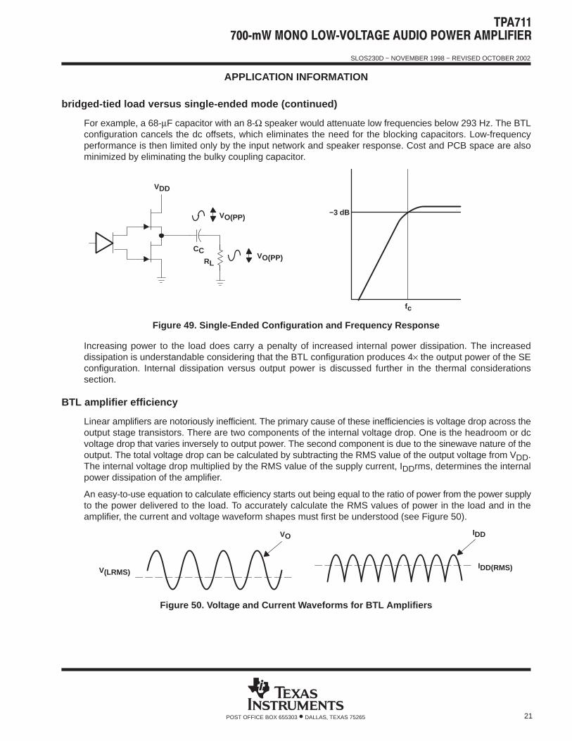
For example, a 68-µF capacitor with an 8-Ω speaker would attenuate low frequencies below 293 Hz. The BTLconfiguration cancels the dc offsets, which eliminates the need for the blocking capacitors. Low-frequencyperformance is then limited only by the input network and speaker response. Cost and PCB space are alsominimized by eliminating the bulky coupling capacitor.
RL
CCVO(PP)
VO(PP)
VDD
−3 dB
fc
Figure 49. Single-Ended Configuration and Frequency Response
Increasing power to the load does carry a penalty of increased internal power dissipation. The increaseddissipation is understandable considering that the BTL configuration produces 4× the output power of the SEconfiguration. Internal dissipation versus output power is discussed further in the thermal considerationssection.
BTL amplifier efficiency
Linear amplifiers are notoriously inefficient. The primary cause of these inefficiencies is voltage drop across theoutput stage transistors. There are two components of the internal voltage drop. One is the headroom or dcvoltage drop that varies inversely to output power. The second component is due to the sinewave nature of theoutput. The total voltage drop can be calculated by subtracting the RMS value of the output voltage from VDD.The internal voltage drop multiplied by the RMS value of the supply current, IDDrms, determines the internalpower dissipation of the amplifier.
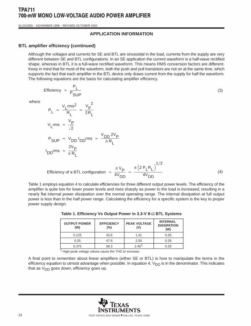
An easy-to-use equation to calculate efficiency starts out being equal to the ratio of power from the power supplyto the power delivered to the load. To accurately calculate the RMS values of power in the load and in theamplifier, the current and voltage waveform shapes must first be understood (see Figure 50).
V(LRMS)
VO IDD
IDD(RMS)
Figure 50. Voltage and Current Waveforms for BTL Amplifiers
SLOS230D − NOVEMBER 1998 − REVISED OCTOBER 2002
22 POST OFFICE BOX 655303 • DALLAS, TEXAS 75265
APPLICATION INFORMATION
BTL amplifier efficiency (continued)
Although the voltages and currents for SE and BTL are sinusoidal in the load, currents from the supply are verydifferent between SE and BTL configurations. In an SE application the current waveform is a half-wave rectifiedshape, whereas in BTL it is a full-wave rectified waveform. This means RMS conversion factors are different.Keep in mind that for most of the waveform, both the push and pull transistors are not on at the same time, whichsupports the fact that each amplifier in the BTL device only draws current from the supply for half the waveform.The following equations are the basis for calculating amplifier efficiency.
IDDrms 2VP RL
PSUP VDD IDDrms VDD 2VP
RL
Efficiency PL
PSUP
Efficiency of a BTL configuration VP4VDD
2 PLRL
12
4VDD
(3)
where
(4)
PL VLrms2
RL
Vp2
2RL
VLrms VP
2
Table 1 employs equation 4 to calculate efficiencies for three different output power levels. The efficiency of theamplifier is quite low for lower power levels and rises sharply as power to the load is increased, resulting in anearly flat internal power dissipation over the normal operating range. The internal dissipation at full outputpower is less than in the half power range. Calculating the efficiency for a specific system is the key to properpower supply design.
Table 1. Efficiency Vs Output Power in 3.3-V 8- Ω BTL Systems
OUTPUT POWER(W)
EFFICIENCY(%)
PEAK VOLTAGE(V)
INTERNAL DISSIPATION
(W)
0.125 33.6 1.41 0.26
0.25 47.6 2.00 0.29
0.375 58.3 2.45† 0.28† High-peak voltage values cause the THD to increase.
A final point to remember about linear amplifiers (either SE or BTL) is how to manipulate the terms in theefficiency equation to utmost advantage when possible. In equation 4, VDD is in the denominator. This indicatesthat as VDD goes down, efficiency goes up.
SLOS230D − NOVEMBER 1998 − REVISED OCTOBER 2002
23POST OFFICE BOX 655303 • DALLAS, TEXAS 75265
APPLICATION INFORMATION
application schematic
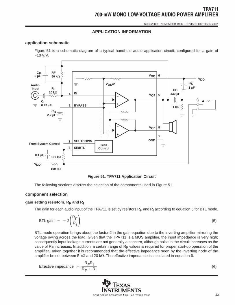
Figure 51 is a schematic diagram of a typical handheld audio application circuit, configured for a gain of−10 V/V.
Audio Input
BiasControl
VDD6
5
7
VO+
VDD
3
1
2
4
BYPASS
IN
SE/BTL
VDD/2
CI0.47 µF
RI10 kΩ
CS1 µF
CB2.2 µF
RF50 kΩ
SHUTDOWN
VO− 8
GNDFrom System Control
CF5 pF
CC330 µF
1 kΩ
100 kΩ
VDD100 kΩ
−
+
−
+
0.1 µF
Figure 51. TPA711 Application Circuit
The following sections discuss the selection of the components used in Figure 51.
component selection
gain setting resistors, R F and RI
The gain for each audio input of the TPA711 is set by resistors RF and RI according to equation 5 for BTL mode.
(5)BTL gain 2RFRI
BTL mode operation brings about the factor 2 in the gain equation due to the inverting amplifier mirroring thevoltage swing across the load. Given that the TPA711 is a MOS amplifier, the input impedance is very high;consequently input leakage currents are not generally a concern, although noise in the circuit increases as thevalue of RF increases. In addition, a certain range of RF values is required for proper start-up operation of theamplifier. Taken together it is recommended that the effective impedance seen by the inverting node of theamplifier be set between 5 kΩ and 20 kΩ. The effective impedance is calculated in equation 6.
(6)Effective impedance RFRI
RF RI
SLOS230D − NOVEMBER 1998 − REVISED OCTOBER 2002
24 POST OFFICE BOX 655303 • DALLAS, TEXAS 75265
APPLICATION INFORMATION
component selection (continued)
As an example consider an input resistance of 10 kΩ and a feedback resistor of 50 kΩ. The BTL gain of theamplifier would be −10 V/V and the effective impedance at the inverting terminal would be 8.3 kΩ, which is wellwithin the recommended range.
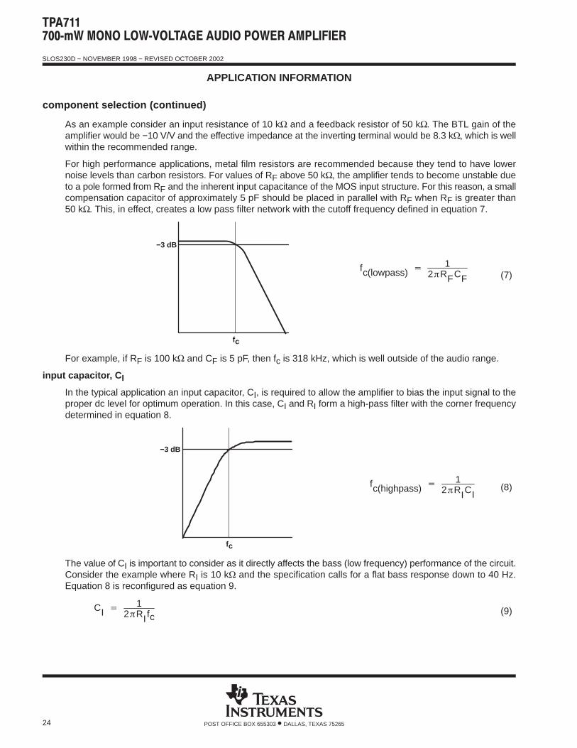
For high performance applications, metal film resistors are recommended because they tend to have lowernoise levels than carbon resistors. For values of RF above 50 kΩ, the amplifier tends to become unstable dueto a pole formed from RF and the inherent input capacitance of the MOS input structure. For this reason, a smallcompensation capacitor of approximately 5 pF should be placed in parallel with RF when RF is greater than50 kΩ. This, in effect, creates a low pass filter network with the cutoff frequency defined in equation 7.
(7)
−3 dB
fc
fc(lowpass) 12RFCF
For example, if RF is 100 kΩ and CF is 5 pF, then fc is 318 kHz, which is well outside of the audio range.
input capacitor, C I
In the typical application an input capacitor, CI, is required to allow the amplifier to bias the input signal to theproper dc level for optimum operation. In this case, CI and RI form a high-pass filter with the corner frequencydetermined in equation 8.
(8)fc(highpass) 12RICI
−3 dB
fc
The value of CI is important to consider as it directly affects the bass (low frequency) performance of the circuit.Consider the example where RI is 10 kΩ and the specification calls for a flat bass response down to 40 Hz.Equation 8 is reconfigured as equation 9.
(9)CI 12RIfc
SLOS230D − NOVEMBER 1998 − REVISED OCTOBER 2002
25POST OFFICE BOX 655303 • DALLAS, TEXAS 75265
APPLICATION INFORMATION
component selection (continued)
In this example, CI is 0.40 µF, so one would likely choose a value in the range of 0.47 µF to 1 µF. A furtherconsideration for this capacitor is the leakage path from the input source through the input network (RI, CI) andthe feedback resistor (RF) to the load. This leakage current creates a dc offset voltage at the input to the amplifierthat reduces useful headroom, especially in high gain applications. For this reason a low-leakage tantalum orceramic capacitor is the best choice. When polarized capacitors are used, the positive side of the capacitorshould face the amplifier input in most applications, as the dc level there is held at VDD/2, which is likely higherthan the source dc level. It is important to confirm the capacitor polarity in the application.
power supply decoupling, C S
The TPA711 is a high-performance CMOS audio amplifier that requires adequate power supply decoupling toensure the output total harmonic distortion (THD) is as low as possible. Power supply decoupling also preventsoscillations for long lead lengths between the amplifier and the speaker. The optimum decoupling is achievedby using two capacitors of different types that target different types of noise on the power supply leads. Forhigher frequency transients, spikes, or digital hash on the line, a good low equivalent-series-resistance (ESR)ceramic capacitor, typically 0.1 µF placed as close as possible to the device VDD lead, works best. For filteringlower-frequency noise signals, a larger aluminum electrolytic capacitor of 10 µF or greater placed near the audiopower amplifier is recommended.
midrail bypass capacitor, C B
The midrail bypass capacitor, CB, is the most critical capacitor and serves several important functions. Duringstart-up or recovery from shutdown mode, CB determines the rate at which the amplifier starts up. The secondfunction is to reduce noise produced by the power supply caused by coupling into the output drive signal. Thisnoise is from the midrail generation circuit internal to the amplifier, which appears as degraded PSRR THD + N. The capacitor is fed from a 250-kΩ source inside the amplifier. To keep the start-up pop as low aspossible, the relationship shown in equation 10 should be maintained. This insures the input capacitor is fullycharged before the bypass capacitor is fully charged and the amplifier starts up.
(10)10
CB 250 kΩ 1RF RI
CI
As an example, consider a circuit where CB is 2.2 µF, CI is 0.47 µF, RF is 50 kΩ, and RI is 10 kΩ. Inserting thesevalues into the equation 10 we get:
18.2 35.5
which satisfies the rule. Bypass capacitor, CB, values of 0.1 µF to 2.2 µF ceramic or tantalum low-ESR capacitorsare recommended for the best THD and noise performance.
single-ended operation
In SE mode (see Figure 51), the load is driven from the primary amplifier output (VO+, terminal 5).
In SE mode the gain is set by the RF and RI resistors and is shown in equation 11. Since the inverting amplifieris not used to mirror the voltage swing on the load, the factor of 2, from equation 5, is not included.
(11)SE Gain RFRI
SLOS230D − NOVEMBER 1998 − REVISED OCTOBER 2002
26 POST OFFICE BOX 655303 • DALLAS, TEXAS 75265
APPLICATION INFORMATION
component selection (continued)
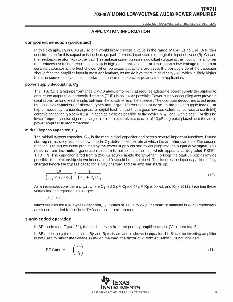
The output coupling capacitor required in single-supply SE mode also places additional constraints on theselection of other components in the amplifier circuit. The rules described earlier still hold with the addition ofthe following relationship:
(12)10
CB 250 kΩ 1
RF RI CI
1RLCC
output coupling capacitor, C C
In the typical single-supply SE configuration, an output coupling capacitor (CC) is required to block the dc biasat the output of the amplifier, thus preventing dc currents in the load. As with the input coupling capacitor, theoutput coupling capacitor and impedance of the load form a high-pass filter governed by equation 13.
(13)fc(high) 12RLCC
−3 dB
fc
The main disadvantage, from a performance standpoint, is the load impedances are typically small, which drivesthe low-frequency corner higher, degrading the bass response. Large values of CC are required to pass lowfrequencies into the load. Consider the example where a CC of 330 µF is chosen and loads vary from 4 Ω,8 Ω, 32 Ω, and 47 kΩ. Table 2 summarizes the frequency response characteristics of each configuration.
Table 2. Common Load Impedances Vs Low Frequency Output Characteristics in SE Mode
RL CC LOWEST FREQUENCY
8 Ω 330 µF 60 Hz
32 Ω 330 µF 15 Hz
47,000 Ω 330 µF 0.01 Hz
As Table 2 indicates, an 8-Ω load is adequate, earphone response is good, and drive into line level inputs (ahome stereo for example) is exceptional.
SLOS230D − NOVEMBER 1998 − REVISED OCTOBER 2002
27POST OFFICE BOX 655303 • DALLAS, TEXAS 75265
APPLICATION INFORMATION
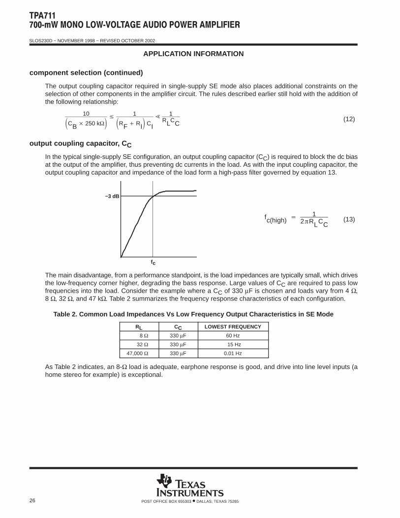
SE/BTL operation
The ability of the TPA711 to easily switch between BTL and SE modes is one of its most important cost-savingfeatures. This feature eliminates the requirement for an additional earphone amplifier in applications whereinternal speakers are driven in BTL mode but external earphone or speaker must be accommodated. Internalto the TPA711, two separate amplifiers drive VO+ and VO−. The SE/BTL input (terminal 3) controls the operationof the follower amplifier that drives VO− (terminal 8). When SE/BTL is held low, the amplifier is on and the TPA711is in the BTL mode. When SE/BTL is held high, the VO− amplifier is in a high output impedance state, whichconfigures the TPA711 as an SE driver from VO+ (terminal 5). IDD is reduced by approximately one-half in SEmode. Control of the SE/BTL input can be from a logic-level TTL source or, more typically, from a resistor dividernetwork as shown in Figure 52.
BiasControl
5
7
VO+
3
1
2
4
BYPASS
IN
SE/BTL
SHUTDOWN
VO− 8
GND
CC
1 kΩ
100 kΩ
VDD100 kΩ
−
+
−
+
0.1 µF
Figure 52. TPA711 Resistor Divider Network Circuit
Using a readily available 1/8-in. (3.5 mm) mono earphone jack, the control switch is closed when no plug isinserted. When closed, the 100-kΩ/1-kΩ divider pulls the SE/BTL input low. When a plug is inserted, the 1-kΩresistor is disconnected and the SE/BTL input is pulled high. When the input goes high, the VO− amplifier is shutdown causing the BTL speaker to mute (virtually open-circuits the speaker). The VO+ amplifier then drivesthrough the output capacitor (CC) into the earphone jack.
using low-ESR capacitors
Low-ESR capacitors are recommended throughout this applications section. A real (as opposed to ideal)capacitor can be modeled simply as a resistor in series with an ideal capacitor. The voltage drop across thisresistor minimizes the beneficial effects of the capacitor in the circuit. The lower the equivalent value of thisresistance the more the real capacitor behaves like an ideal capacitor.
SLOS230D − NOVEMBER 1998 − REVISED OCTOBER 2002
28 POST OFFICE BOX 655303 • DALLAS, TEXAS 75265
APPLICATION INFORMATION
5-V versus 3.3-V operation
The TPA711 operates over a supply range of 2.5 V to 5.5 V. This data sheet provides full specifications for 5-Vand 3.3-V operation, as these are considered to be the two most common standard voltages. There are nospecial considerations for 3.3-V versus 5-V operation with respect to supply bypassing, gain setting, or stability.The most important consideration is that of output power. Each amplifier in TPA711 can produce a maximumvoltage swing of VDD − 1 V. This means, for 3.3-V operation, clipping starts to occur when VO(PP) = 2.3 V asopposed to VO(PP) = 4 V at 5 V. The reduced voltage swing subsequently reduces maximum output power intoan 8-Ω load before distortion becomes significant.
Operation from 3.3-V supplies, as can be shown from the efficiency formula in equation 4, consumesapproximately two-thirds the supply power of operation from 5-V supplies for a given output-power level.
headroom and thermal considerations
Linear power amplifiers dissipate a significant amount of heat in the package under normal operating conditions.A typical music CD requires 12 dB to 15 dB of dynamic headroom to pass the loudest portions without distortionas compared with the average power output. From the TPA711 data sheet, one can see that when the TPA711is operating from a 5-V supply into a 8-Ω speaker that 700 mW peaks are available. Converting watts to dB:
PdB 10LogPWPref 10Log 700 mW
1W –1.5 dB
Subtracting the headroom restriction to obtain the average listening level without distortion yields:
−1.5 dB − 15 dB = −16.5 (15 dB headroom)−1.5 dB − 12 dB = −13.5 (12 dB headroom)−1.5 dB − 9 dB = −10.5 (9 dB headroom)−1.5 dB − 6 dB = −7.5 (6 dB headroom)−1.5 dB − 3 dB = −4.5 (3 dB headroom)
Converting dB back into watts:
PW 10PdB10 Pref 22 mW (15 dB headroom)
44 mW (12 dB headroom)
88 mW (9 dB headroom)
175 mW (6 dB headroom)
350 mW (3 dB headroom)
SLOS230D − NOVEMBER 1998 − REVISED OCTOBER 2002
29POST OFFICE BOX 655303 • DALLAS, TEXAS 75265
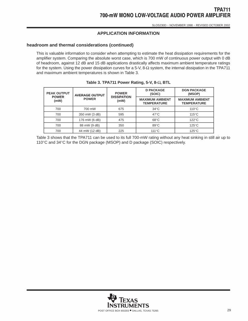
APPLICATION INFORMATION
headroom and thermal considerations (continued)
This is valuable information to consider when attempting to estimate the heat dissipation requirements for theamplifier system. Comparing the absolute worst case, which is 700 mW of continuous power output with 0 dBof headroom, against 12 dB and 15 dB applications drastically affects maximum ambient temperature ratingsfor the system. Using the power dissipation curves for a 5-V, 8-Ω system, the internal dissipation in the TPA711and maximum ambient temperatures is shown in Table 3.
Table 3. TPA711 Power Rating, 5-V, 8- Ω, BTL
PEAK OUTPUTPOWER AVERAGE OUTPUT
POWERDISSIPATION
D PACKAGE(SOIC)
DGN PACKAGE(MSOP)
POWER(mW)
AVERAGE OUTPUTPOWER
DISSIPATION(mW) MAXIMUM AMBIENT
TEMPERATUREMAXIMUM AMBIENT
TEMPERATURE
700 700 mW 675 34°C 110°C
700 350 mW (3 dB) 595 47°C 115°C
700 176 mW (6 dB) 475 68°C 122°C
700 88 mW (9 dB) 350 89°C 125°C
700 44 mW (12 dB) 225 111°C 125°C
Table 3 shows that the TPA711 can be used to its full 700-mW rating without any heat sinking in still air up to110°C and 34°C for the DGN package (MSOP) and D package (SOIC) respectively.
PACKAGE OPTION ADDENDUM
www.ti.com 8-Sep-2017
Addendum-Page 1
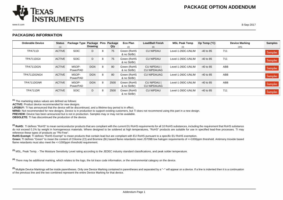
PACKAGING INFORMATION
Orderable Device Status(1)
Package Type PackageDrawing
Pins PackageQty
Eco Plan(2)
Lead/Ball Finish(6)
MSL Peak Temp(3)
Op Temp (°C) Device Marking(4/5)
Samples
TPA711D ACTIVE SOIC D 8 75 Green (RoHS& no Sb/Br)
CU NIPDAU Level-1-260C-UNLIM -40 to 85 711
TPA711DG4 ACTIVE SOIC D 8 75 Green (RoHS& no Sb/Br)
CU NIPDAU Level-1-260C-UNLIM -40 to 85 711
TPA711DGN ACTIVE MSOP-PowerPAD
DGN 8 80 Green (RoHS& no Sb/Br)
CU NIPDAU |CU NIPDAUAG
Level-1-260C-UNLIM -40 to 85 ABB
TPA711DGNG4 ACTIVE MSOP-PowerPAD
DGN 8 80 Green (RoHS& no Sb/Br)
CU NIPDAUAG Level-1-260C-UNLIM -40 to 85 ABB
TPA711DGNR ACTIVE MSOP-PowerPAD
DGN 8 2500 Green (RoHS& no Sb/Br)
CU NIPDAU |CU NIPDAUAG
Level-1-260C-UNLIM -40 to 85 ABB
TPA711DR ACTIVE SOIC D 8 2500 Green (RoHS& no Sb/Br)
CU NIPDAU Level-1-260C-UNLIM -40 to 85 711
(1) The marketing status values are defined as follows:ACTIVE: Product device recommended for new designs.LIFEBUY: TI has announced that the device will be discontinued, and a lifetime-buy period is in effect.NRND: Not recommended for new designs. Device is in production to support existing customers, but TI does not recommend using this part in a new design.PREVIEW: Device has been announced but is not in production. Samples may or may not be available.OBSOLETE: TI has discontinued the production of the device.
(2) RoHS: TI defines "RoHS" to mean semiconductor products that are compliant with the current EU RoHS requirements for all 10 RoHS substances, including the requirement that RoHS substancedo not exceed 0.1% by weight in homogeneous materials. Where designed to be soldered at high temperatures, "RoHS" products are suitable for use in specified lead-free processes. TI mayreference these types of products as "Pb-Free".RoHS Exempt: TI defines "RoHS Exempt" to mean products that contain lead but are compliant with EU RoHS pursuant to a specific EU RoHS exemption.Green: TI defines "Green" to mean the content of Chlorine (Cl) and Bromine (Br) based flame retardants meet JS709B low halogen requirements of <=1000ppm threshold. Antimony trioxide basedflame retardants must also meet the <=1000ppm threshold requirement.
(3) MSL, Peak Temp. - The Moisture Sensitivity Level rating according to the JEDEC industry standard classifications, and peak solder temperature.
(4) There may be additional marking, which relates to the logo, the lot trace code information, or the environmental category on the device.
(5) Multiple Device Markings will be inside parentheses. Only one Device Marking contained in parentheses and separated by a "~" will appear on a device. If a line is indented then it is a continuationof the previous line and the two combined represent the entire Device Marking for that device.
PACKAGE OPTION ADDENDUM
www.ti.com 8-Sep-2017
Addendum-Page 2
(6) Lead/Ball Finish - Orderable Devices may have multiple material finish options. Finish options are separated by a vertical ruled line. Lead/Ball Finish values may wrap to two lines if the finishvalue exceeds the maximum column width.
Important Information and Disclaimer:The information provided on this page represents TI's knowledge and belief as of the date that it is provided. TI bases its knowledge and belief on informationprovided by third parties, and makes no representation or warranty as to the accuracy of such information. Efforts are underway to better integrate information from third parties. TI has taken andcontinues to take reasonable steps to provide representative and accurate information but may not have conducted destructive testing or chemical analysis on incoming materials and chemicals.TI and TI suppliers consider certain information to be proprietary, and thus CAS numbers and other limited information may not be available for release.
In no event shall TI's liability arising out of such information exceed the total purchase price of the TI part(s) at issue in this document sold by TI to Customer on an annual basis.
TAPE AND REEL INFORMATION
*All dimensions are nominal
Device PackageType
PackageDrawing
Pins SPQ ReelDiameter
(mm)
ReelWidth
W1 (mm)
A0(mm)
B0(mm)
K0(mm)
P1(mm)
W(mm)
Pin1Quadrant
TPA711DGNR MSOP-Power PAD
DGN 8 2500 330.0 12.4 5.3 3.4 1.4 8.0 12.0 Q1
TPA711DGNR MSOP-Power PAD
DGN 8 2500 330.0 12.4 5.3 3.4 1.4 8.0 12.0 Q1
TPA711DR SOIC D 8 2500 330.0 12.4 6.4 5.2 2.1 8.0 12.0 Q1
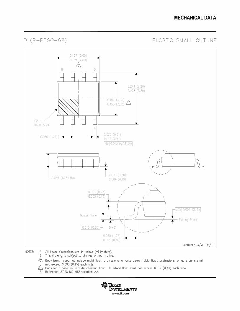
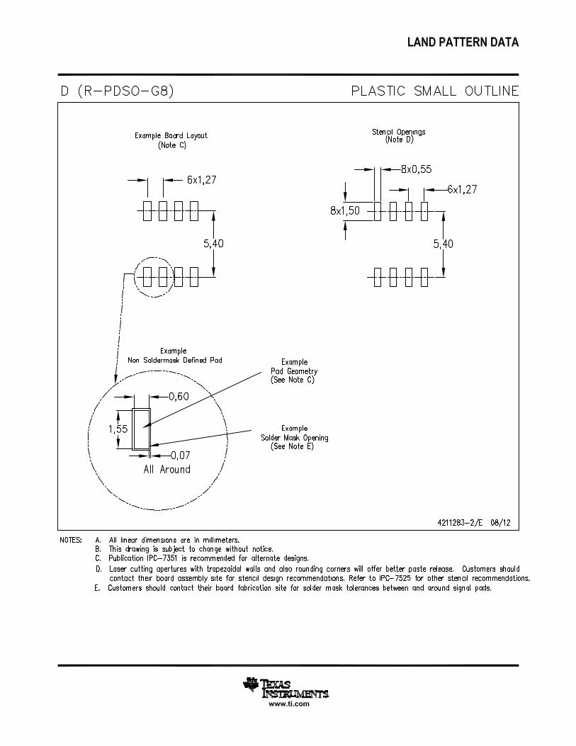
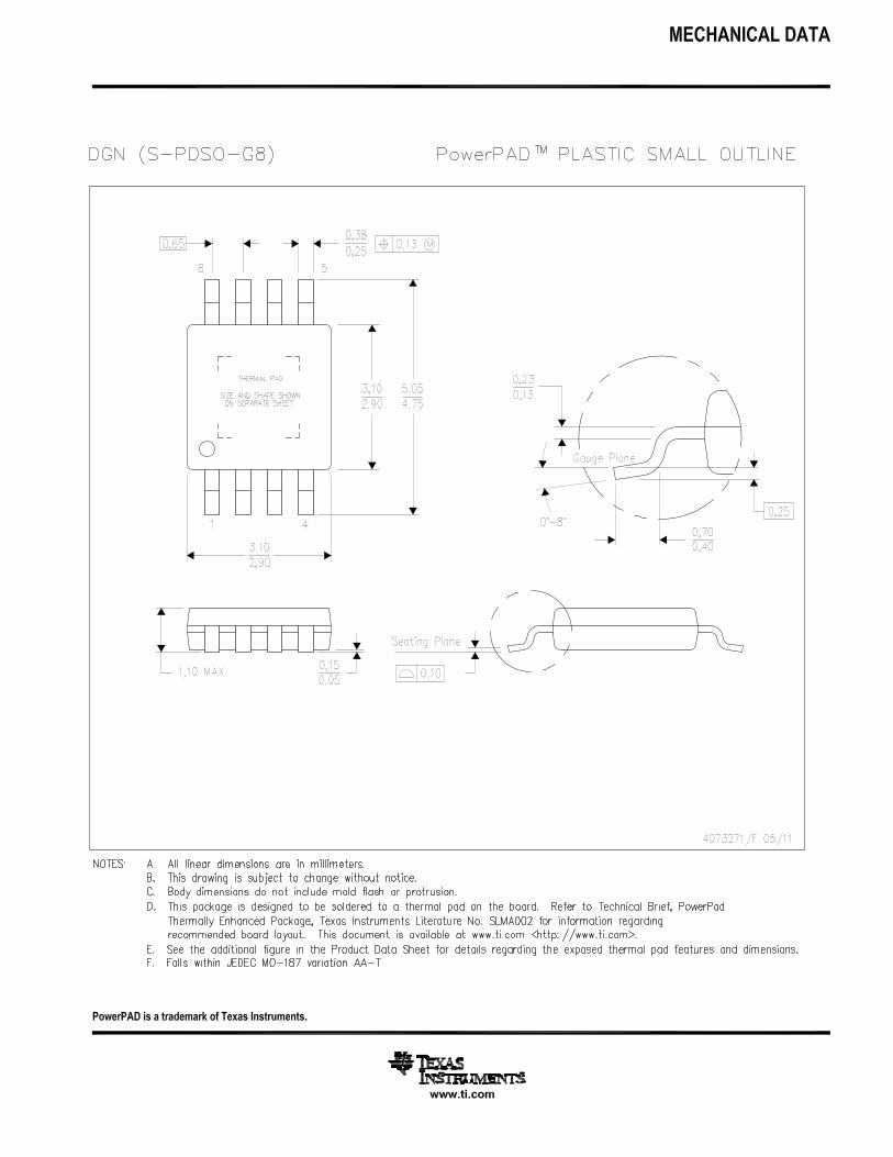
PACKAGE MATERIALS INFORMATION
www.ti.com 3-Aug-2017
Pack Materials-Page 1
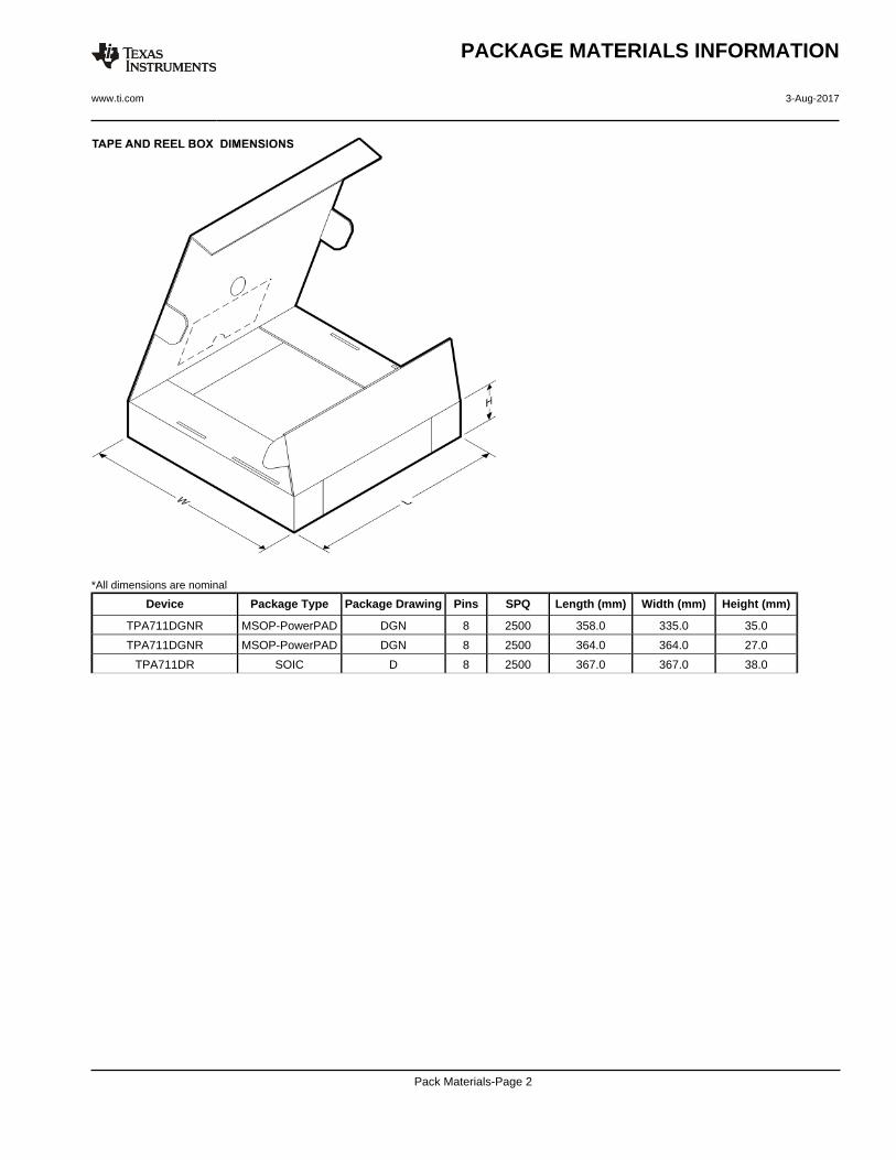
*All dimensions are nominal
Device Package Type Package Drawing Pins SPQ Length (mm) Width (mm) Height (mm)
TPA711DGNR MSOP-PowerPAD DGN 8 2500 358.0 335.0 35.0
TPA711DGNR MSOP-PowerPAD DGN 8 2500 364.0 364.0 27.0
TPA711DR SOIC D 8 2500 367.0 367.0 38.0
PACKAGE MATERIALS INFORMATION
www.ti.com 3-Aug-2017
Pack Materials-Page 2

IMPORTANT NOTICE
Texas Instruments Incorporated (TI) reserves the right to make corrections, enhancements, improvements and other changes to itssemiconductor products and services per JESD46, latest issue, and to discontinue any product or service per JESD48, latest issue. Buyersshould obtain the latest relevant information before placing orders and should verify that such information is current and complete.TI’s published terms of sale for semiconductor products (http://www.ti.com/sc/docs/stdterms.htm) apply to the sale of packaged integratedcircuit products that TI has qualified and released to market. Additional terms may apply to the use or sale of other types of TI products andservices.Reproduction of significant portions of TI information in TI data sheets is permissible only if reproduction is without alteration and isaccompanied by all associated warranties, conditions, limitations, and notices. TI is not responsible or liable for such reproduceddocumentation. Information of third parties may be subject to additional restrictions. Resale of TI products or services with statementsdifferent from or beyond the parameters stated by TI for that product or service voids all express and any implied warranties for theassociated TI product or service and is an unfair and deceptive business practice. TI is not responsible or liable for any such statements.Buyers and others who are developing systems that incorporate TI products (collectively, “Designers”) understand and agree that Designersremain responsible for using their independent analysis, evaluation and judgment in designing their applications and that Designers havefull and exclusive responsibility to assure the safety of Designers' applications and compliance of their applications (and of all TI productsused in or for Designers’ applications) with all applicable regulations, laws and other applicable requirements. Designer represents that, withrespect to their applications, Designer has all the necessary expertise to create and implement safeguards that (1) anticipate dangerousconsequences of failures, (2) monitor failures and their consequences, and (3) lessen the likelihood of failures that might cause harm andtake appropriate actions. Designer agrees that prior to using or distributing any applications that include TI products, Designer willthoroughly test such applications and the functionality of such TI products as used in such applications.TI’s provision of technical, application or other design advice, quality characterization, reliability data or other services or information,including, but not limited to, reference designs and materials relating to evaluation modules, (collectively, “TI Resources”) are intended toassist designers who are developing applications that incorporate TI products; by downloading, accessing or using TI Resources in anyway, Designer (individually or, if Designer is acting on behalf of a company, Designer’s company) agrees to use any particular TI Resourcesolely for this purpose and subject to the terms of this Notice.TI’s provision of TI Resources does not expand or otherwise alter TI’s applicable published warranties or warranty disclaimers for TIproducts, and no additional obligations or liabilities arise from TI providing such TI Resources. TI reserves the right to make corrections,enhancements, improvements and other changes to its TI Resources. TI has not conducted any testing other than that specificallydescribed in the published documentation for a particular TI Resource.Designer is authorized to use, copy and modify any individual TI Resource only in connection with the development of applications thatinclude the TI product(s) identified in such TI Resource. NO OTHER LICENSE, EXPRESS OR IMPLIED, BY ESTOPPEL OR OTHERWISETO ANY OTHER TI INTELLECTUAL PROPERTY RIGHT, AND NO LICENSE TO ANY TECHNOLOGY OR INTELLECTUAL PROPERTYRIGHT OF TI OR ANY THIRD PARTY IS GRANTED HEREIN, including but not limited to any patent right, copyright, mask work right, orother intellectual property right relating to any combination, machine, or process in which TI products or services are used. Informationregarding or referencing third-party products or services does not constitute a license to use such products or services, or a warranty orendorsement thereof. Use of TI Resources may require a license from a third party under the patents or other intellectual property of thethird party, or a license from TI under the patents or other intellectual property of TI.TI RESOURCES ARE PROVIDED “AS IS” AND WITH ALL FAULTS. TI DISCLAIMS ALL OTHER WARRANTIES ORREPRESENTATIONS, EXPRESS OR IMPLIED, REGARDING RESOURCES OR USE THEREOF, INCLUDING BUT NOT LIMITED TOACCURACY OR COMPLETENESS, TITLE, ANY EPIDEMIC FAILURE WARRANTY AND ANY IMPLIED WARRANTIES OFMERCHANTABILITY, FITNESS FOR A PARTICULAR PURPOSE, AND NON-INFRINGEMENT OF ANY THIRD PARTY INTELLECTUALPROPERTY RIGHTS. TI SHALL NOT BE LIABLE FOR AND SHALL NOT DEFEND OR INDEMNIFY DESIGNER AGAINST ANY CLAIM,INCLUDING BUT NOT LIMITED TO ANY INFRINGEMENT CLAIM THAT RELATES TO OR IS BASED ON ANY COMBINATION OFPRODUCTS EVEN IF DESCRIBED IN TI RESOURCES OR OTHERWISE. IN NO EVENT SHALL TI BE LIABLE FOR ANY ACTUAL,DIRECT, SPECIAL, COLLATERAL, INDIRECT, PUNITIVE, INCIDENTAL, CONSEQUENTIAL OR EXEMPLARY DAMAGES INCONNECTION WITH OR ARISING OUT OF TI RESOURCES OR USE THEREOF, AND REGARDLESS OF WHETHER TI HAS BEENADVISED OF THE POSSIBILITY OF SUCH DAMAGES.Unless TI has explicitly designated an individual product as meeting the requirements of a particular industry standard (e.g., ISO/TS 16949and ISO 26262), TI is not responsible for any failure to meet such industry standard requirements.Where TI specifically promotes products as facilitating functional safety or as compliant with industry functional safety standards, suchproducts are intended to help enable customers to design and create their own applications that meet applicable functional safety standardsand requirements. Using products in an application does not by itself establish any safety features in the application. Designers mustensure compliance with safety-related requirements and standards applicable to their applications. Designer may not use any TI products inlife-critical medical equipment unless authorized officers of the parties have executed a special contract specifically governing such use.Life-critical medical equipment is medical equipment where failure of such equipment would cause serious bodily injury or death (e.g., lifesupport, pacemakers, defibrillators, heart pumps, neurostimulators, and implantables). Such equipment includes, without limitation, allmedical devices identified by the U.S. Food and Drug Administration as Class III devices and equivalent classifications outside the U.S.TI may expressly designate certain products as completing a particular qualification (e.g., Q100, Military Grade, or Enhanced Product).Designers agree that it has the necessary expertise to select the product with the appropriate qualification designation for their applicationsand that proper product selection is at Designers’ own risk. Designers are solely responsible for compliance with all legal and regulatoryrequirements in connection with such selection.Designer will fully indemnify TI and its representatives against any damages, costs, losses, and/or liabilities arising out of Designer’s non-compliance with the terms and provisions of this Notice.
Mailing Address: Texas Instruments, Post Office Box 655303, Dallas, Texas 75265Copyright © 2017, Texas Instruments Incorporated


![CHARAKTERYSTYKI STAŁOPRĄDOWE … · dsp =β p V in −V DD −V tp] 2 [( ) 2 1 2 out dsn n in tn out V I =βV −V V ...](https://static.fdocument.org/doc/165x107/5b96032409d3f2d7438d1c5c/charakterystyki-stalopradowe-dsp-p-v-in-v-dd-v-tp-2-2-1-2.jpg)