8-Bit Latch With 3-State Outputs - TI.com · CY74FCT2573T 8-BIT LATCH WITH 3-STATE OUTPUTS SCCS075...
15
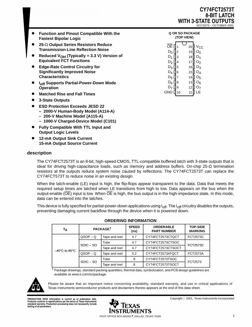
CY74FCT2573T 8-BIT LATCH WITH 3-STATE OUTPUTS SCCS075 – OCTOBER 2001 1 POST OFFICE BOX 655303 • DALLAS, TEXAS 75265 Function and Pinout Compatible With the Fastest Bipolar Logic 25-Ω Output Series Resistors Reduce Transmission-Line Reflection Noise Reduced V OH (Typically = 3.3 V) Version of Equivalent FCT Functions Edge-Rate Control Circuitry for Significantly Improved Noise Characteristics I off Supports Partial-Power-Down Mode Operation Matched Rise and Fall Times 3-State Outputs ESD Protection Exceeds JESD 22 – 2000-V Human-Body Model (A114-A) – 200-V Machine Model (A115-A) – 1000-V Charged-Device Model (C101) Fully Compatible With TTL Input and Output Logic Levels 12-mA Output Sink Current 15-mA Output Source Current description The CY74FCT2573T is an 8-bit, high-speed CMOS, TTL-compatible buffered latch with 3-state outputs that is ideal for driving high-capacitance loads, such as memory and address buffers. On-chip 25-Ω termination resistors at the outputs reduce system noise caused by reflections. The CY74FCT2573T can replace the CY74FCT573T to reduce noise in an existing design. When the latch-enable (LE) input is high, the flip-flops appear transparent to the data. Data that meets the required setup times are latched when LE transitions from high to low. Data appears on the bus when the output-enable (OE ) input is low. When OE is high, the bus output is in the high-impedance state. In this mode, data can be entered into the latches. This device is fully specified for partial-power-down applications using I off . The I off circuitry disables the outputs, preventing damaging current backflow through the device when it is powered down. ORDERING INFORMATION T A PACKAGE † SPEED (ns) ORDERABLE PART NUMBER TOP-SIDE MARKING QSOP – Q Tape and reel 4.7 CY74FCT2573CTQCT FCT2573C SOIC SO Tube 4.7 CY74FCT2573CTSOC FCT2573C 40°C to 85°C SOIC – SO Tape and reel 4.7 CY74FCT2573CTSOCT FCT2573C –40°C to 85°C QSOP – Q Tape and reel 5.2 CY74FCT2573ATQCT FCT2573A SOIC SO Tube 8 CY74FCT2573TSOC FCT2573 SOIC – SO Tape and reel 8 CY74FCT2573TSOCT FCT2573 † Package drawings, standard packing quantities, thermal data, symbolization, and PCB design guidelines are available at www.ti.com/sc/package. Copyright 2001, Texas Instruments Incorporated PRODUCTION DATA information is current as of publication date. Products conform to specifications per the terms of Texas Instruments standard warranty. Production processing does not necessarily include testing of all parameters. Please be aware that an important notice concerning availability, standard warranty, and use in critical applications of Texas Instruments semiconductor products and disclaimers thereto appears at the end of this data sheet. OE D 0 D 1 D 2 D 3 D 4 D 5 D 6 D 7 GND Q OR SO PACKAGE (TOP VIEW) 1 2 3 4 5 6 7 8 9 10 20 19 18 17 16 15 14 13 12 11 V CC O 0 O 1 O 2 O 3 O 4 O 5 O 6 O 7 LE
Transcript of 8-Bit Latch With 3-State Outputs - TI.com · CY74FCT2573T 8-BIT LATCH WITH 3-STATE OUTPUTS SCCS075...
CY74FCT2573T8-BIT LATCH
WITH 3-STATE OUTPUTS
SCCS075 – OCTOBER 2001
1POST OFFICE BOX 655303 • DALLAS, TEXAS 75265
Function and Pinout Compatible With theFastest Bipolar Logic
25-Ω Output Series Resistors ReduceTransmission-Line Reflection Noise
Reduced VOH (Typically = 3.3 V) Version ofEquivalent FCT Functions
Edge-Rate Control Circuitry forSignificantly Improved NoiseCharacteristics
Ioff Supports Partial-Power-Down ModeOperation
Matched Rise and Fall Times
3-State Outputs
ESD Protection Exceeds JESD 22– 2000-V Human-Body Model (A114-A)– 200-V Machine Model (A115-A)– 1000-V Charged-Device Model (C101)
Fully Compatible With TTL Input andOutput Logic Levels
12-mA Output Sink Current15-mA Output Source Current
description
The CY74FCT2573T is an 8-bit, high-speed CMOS, TTL-compatible buffered latch with 3-state outputs that isideal for driving high-capacitance loads, such as memory and address buffers. On-chip 25-Ω terminationresistors at the outputs reduce system noise caused by reflections. The CY74FCT2573T can replace theCY74FCT573T to reduce noise in an existing design.
When the latch-enable (LE) input is high, the flip-flops appear transparent to the data. Data that meets therequired setup times are latched when LE transitions from high to low. Data appears on the bus when theoutput-enable (OE) input is low. When OE is high, the bus output is in the high-impedance state. In this mode,data can be entered into the latches.
This device is fully specified for partial-power-down applications using Ioff. The Ioff circuitry disables the outputs,preventing damaging current backflow through the device when it is powered down.
ORDERING INFORMATION
TA PACKAGE† SPEED(ns)
ORDERABLEPART NUMBER
TOP-SIDEMARKING
QSOP – Q Tape and reel 4.7 CY74FCT2573CTQCT FCT2573C
SOIC SOTube 4.7 CY74FCT2573CTSOC
FCT2573C
40°C to 85°C
SOIC – SOTape and reel 4.7 CY74FCT2573CTSOCT
FCT2573C
–40°C to 85°CQSOP – Q Tape and reel 5.2 CY74FCT2573ATQCT FCT2573A
SOIC SOTube 8 CY74FCT2573TSOC
FCT2573SOIC – SOTape and reel 8 CY74FCT2573TSOCT
FCT2573
† Package drawings, standard packing quantities, thermal data, symbolization, and PCB design guidelines areavailable at www.ti.com/sc/package.
Copyright 2001, Texas Instruments IncorporatedPRODUCTION DATA information is current as of publication date.Products conform to specifications per the terms of Texas Instrumentsstandard warranty. Production processing does not necessarily includetesting of all parameters.
Please be aware that an important notice concerning availability, standard warranty, and use in critical applications ofTexas Instruments semiconductor products and disclaimers thereto appears at the end of this data sheet.
OED0D1D2D3D4D5D6D7
GND
Q OR SO PACKAGE(TOP VIEW)
1
2
3
4
5
6
7
8
9
10
20
19
18
17
16
15
14
13
12
11
VCCO0O1O2O3O4O5O6O7LE
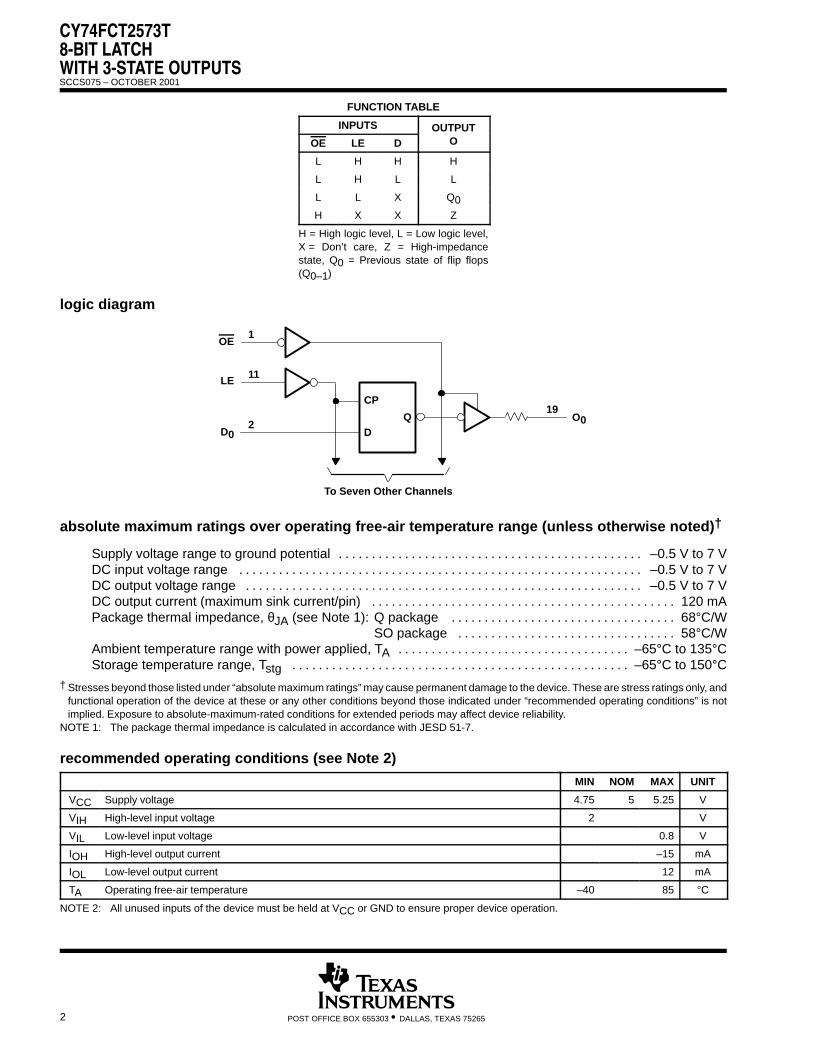
CY74FCT2573T8-BIT LATCHWITH 3-STATE OUTPUTS
SCCS075 – OCTOBER 2001
2 POST OFFICE BOX 655303 • DALLAS, TEXAS 75265
FUNCTION TABLE
INPUTS OUTPUTOE LE D O
L H H H
L H L L
L L X Q0
H X X Z
H = High logic level, L = Low logic level,X = Don’t care, Z = High-impedancestate, Q0 = Previous state of flip flops(Q0–1)
logic diagram
OE
LE
CP
DQ
To Seven Other Channels
D0
O0
1
11
219
absolute maximum ratings over operating free-air temperature range (unless otherwise noted)†
Supply voltage range to ground potential –0.5 V to 7 V. . . . . . . . . . . . . . . . . . . . . . . . . . . . . . . . . . . . . . . . . . . . . . DC input voltage range –0.5 V to 7 V. . . . . . . . . . . . . . . . . . . . . . . . . . . . . . . . . . . . . . . . . . . . . . . . . . . . . . . . . . . . . DC output voltage range –0.5 V to 7 V. . . . . . . . . . . . . . . . . . . . . . . . . . . . . . . . . . . . . . . . . . . . . . . . . . . . . . . . . . . . DC output current (maximum sink current/pin) 120 mA. . . . . . . . . . . . . . . . . . . . . . . . . . . . . . . . . . . . . . . . . . . . . . Package thermal impedance, θJA (see Note 1): Q package 68°C/W. . . . . . . . . . . . . . . . . . . . . . . . . . . . . . . . . .
SO package 58°C/W. . . . . . . . . . . . . . . . . . . . . . . . . . . . . . . . . Ambient temperature range with power applied, TA –65°C to 135°C. . . . . . . . . . . . . . . . . . . . . . . . . . . . . . . . . . . Storage temperature range, Tstg –65°C to 150°C. . . . . . . . . . . . . . . . . . . . . . . . . . . . . . . . . . . . . . . . . . . . . . . . . . .
† Stresses beyond those listed under “absolute maximum ratings” may cause permanent damage to the device. These are stress ratings only, andfunctional operation of the device at these or any other conditions beyond those indicated under “recommended operating conditions” is notimplied. Exposure to absolute-maximum-rated conditions for extended periods may affect device reliability.
NOTE 1: The package thermal impedance is calculated in accordance with JESD 51-7.
recommended operating conditions (see Note 2)
MIN NOM MAX UNIT
VCC Supply voltage 4.75 5 5.25 V
VIH High-level input voltage 2 V
VIL Low-level input voltage 0.8 V
IOH High-level output current –15 mA
IOL Low-level output current 12 mA
TA Operating free-air temperature –40 85 °C
NOTE 2: All unused inputs of the device must be held at VCC or GND to ensure proper device operation.
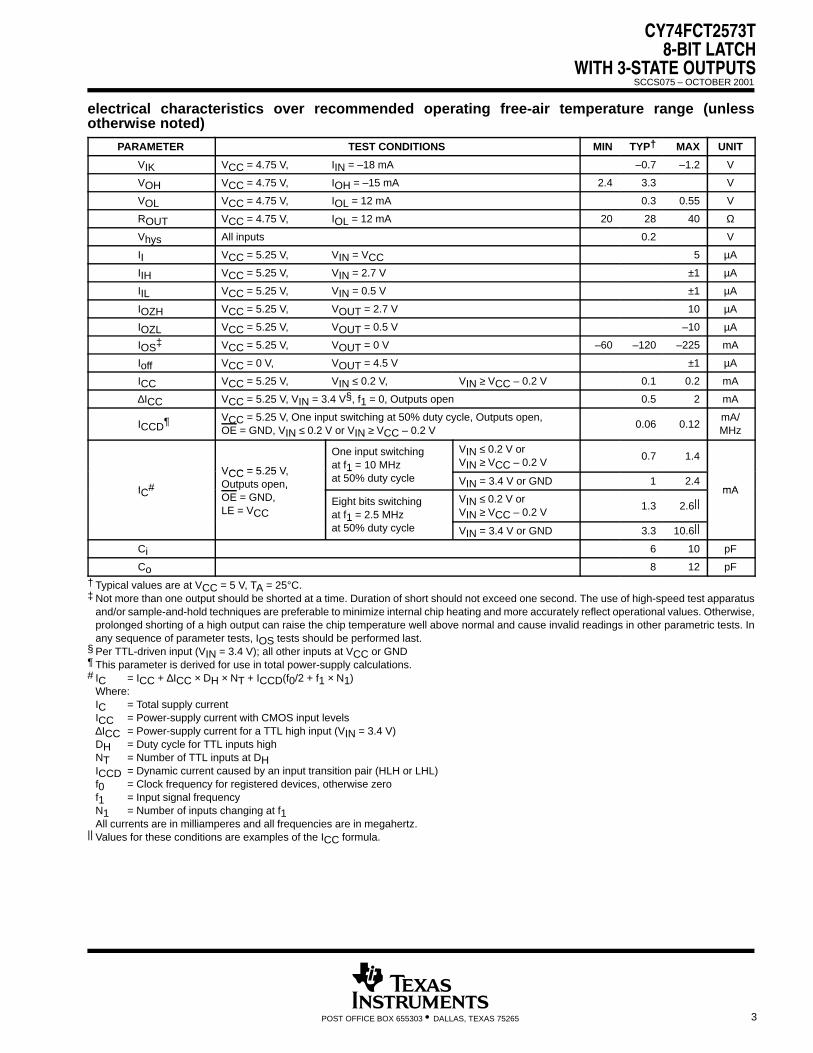
CY74FCT2573T8-BIT LATCH
WITH 3-STATE OUTPUTS
SCCS075 – OCTOBER 2001
3POST OFFICE BOX 655303 • DALLAS, TEXAS 75265
electrical characteristics over recommended operating free-air temperature range (unlessotherwise noted)
PARAMETER TEST CONDITIONS MIN TYP† MAX UNIT
VIK VCC = 4.75 V, IIN = –18 mA –0.7 –1.2 V
VOH VCC = 4.75 V, IOH = –15 mA 2.4 3.3 V
VOL VCC = 4.75 V, IOL = 12 mA 0.3 0.55 V
ROUT VCC = 4.75 V, IOL = 12 mA 20 28 40 Ω
Vhys All inputs 0.2 V
II VCC = 5.25 V, VIN = VCC 5 µA
IIH VCC = 5.25 V, VIN = 2.7 V ±1 µA
IIL VCC = 5.25 V, VIN = 0.5 V ±1 µA
IOZH VCC = 5.25 V, VOUT = 2.7 V 10 µA
IOZL VCC = 5.25 V, VOUT = 0.5 V –10 µA
IOS‡ VCC = 5.25 V, VOUT = 0 V –60 –120 –225 mA
Ioff VCC = 0 V, VOUT = 4.5 V ±1 µA
ICC VCC = 5.25 V, VIN ≤ 0.2 V, VIN ≥ VCC – 0.2 V 0.1 0.2 mA
∆ICC VCC = 5.25 V, VIN = 3.4 V§, f1 = 0, Outputs open 0.5 2 mA
ICCD¶ VCC = 5.25 V, One input switching at 50% duty cycle, Outputs open,OE = GND, VIN ≤ 0.2 V or VIN ≥ VCC – 0.2 V
0.06 0.12mA/MHz
#
VCC = 5 25 V
One input switchingat f1 = 10 MHz
VIN ≤ 0.2 V orVIN ≥ VCC – 0.2 V
0.7 1.4
IC#
VCC = 5.25 V,Outputs open,
1at 50% duty cycle VIN = 3.4 V or GND 1 2.4
mAIC# ,OE = GND,LE = VCC
Eight bits switchingat f1 = 2.5 MHz
VIN ≤ 0.2 V orVIN ≥ VCC – 0.2 V
1.3 2.6||mA
1at 50% duty cycle VIN = 3.4 V or GND 3.3 10.6||
Ci 6 10 pF
Co 8 12 pF
† Typical values are at VCC = 5 V, TA = 25°C.‡ Not more than one output should be shorted at a time. Duration of short should not exceed one second. The use of high-speed test apparatus
and/or sample-and-hold techniques are preferable to minimize internal chip heating and more accurately reflect operational values. Otherwise,prolonged shorting of a high output can raise the chip temperature well above normal and cause invalid readings in other parametric tests. Inany sequence of parameter tests, IOS tests should be performed last.
§ Per TTL-driven input (VIN = 3.4 V); all other inputs at VCC or GND¶ This parameter is derived for use in total power-supply calculations.# IC = ICC + ∆ICC × DH × NT + ICCD(f0/2 + f1 × N1)
Where:IC = Total supply currentICC = Power-supply current with CMOS input levels∆ICC = Power-supply current for a TTL high input (VIN = 3.4 V)DH = Duty cycle for TTL inputs highNT = Number of TTL inputs at DHICCD = Dynamic current caused by an input transition pair (HLH or LHL)f0 = Clock frequency for registered devices, otherwise zerof1 = Input signal frequencyN1 = Number of inputs changing at f1All currents are in milliamperes and all frequencies are in megahertz.
|| Values for these conditions are examples of the ICC formula.

CY74FCT2573T8-BIT LATCHWITH 3-STATE OUTPUTS
SCCS075 – OCTOBER 2001
4 POST OFFICE BOX 655303 • DALLAS, TEXAS 75265
timing requirements over recommended operating free-air temperature range (unless otherwisenoted) (see Figure 1)
CY74FCT2573T CY74FCT2573AT CY74FCT2573CTUNIT
MIN MAX MIN MAX MIN MAXUNIT
tw Pulse duration, LE high 6 5 5 ns
tsu Setup time, D to LE High to low 2 2 2 ns
th Hold time, D to LE High to low 1.5 1.5 1.5 ns
switching characteristics over operating free-air temperature range (see Figure 1)
PARAMETERFROM TO CY74FCT2573T CY74FCT2573AT CY74FCT2573CT
UNITPARAMETER (INPUT) (OUTPUT) MIN MAX MIN MAX MIN MAXUNIT
tPLHD O
1.5 8 1.5 5.2 1.5 4.7ns
tPHLD O
1.5 8 1.5 5.2 1.5 4.7ns
tPLHLE O
2 13 2 8.5 2 5.5ns
tPHLLE O
2 13 2 8.5 2 5.5ns
tPZHOE O
1.5 11 1.5 6.5 1.5 5.5ns
tPZLOE O
1.5 11 1.5 6.5 1.5 5.5ns
tPHZOE O
1.5 7 1.5 5.5 1.5 5ns
tPLZOE O
1.5 7 1.5 5.5 1.5 5ns
CY74FCT2573T8-BIT LATCH
WITH 3-STATE OUTPUTS
SCCS075 – OCTOBER 2001
5POST OFFICE BOX 655303 • DALLAS, TEXAS 75265
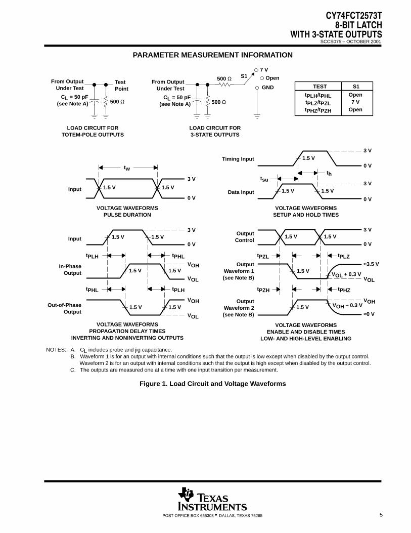
PARAMETER MEASUREMENT INFORMATION
3 V
3 V
0 V
0 V
thtsu
VOLTAGE WAVEFORMSSETUP AND HOLD TIMES
Data Input
tPLH
tPHL
tPHL
tPLH
VOH
VOH
VOL
VOL
3 V
0 VInput
Out-of-PhaseOutput
In-PhaseOutput
Timing Input
VOLTAGE WAVEFORMSPROPAGATION DELAY TIMES
INVERTING AND NONINVERTING OUTPUTS
OutputControl
OutputWaveform 1(see Note B)
OutputWaveform 2(see Note B)
VOL
VOH
tPZL
tPZH
tPLZ
tPHZ
≈3.5 V
0 V
VOL + 0.3 V
≈0 V
3 V
VOLTAGE WAVEFORMSENABLE AND DISABLE TIMES
LOW- AND HIGH-LEVEL ENABLING
tPLH/tPHLtPLZ/tPZLtPHZ/tPZH
Open7 V
Open
TEST S1
3 V
0 V
tw
VOLTAGE WAVEFORMSPULSE DURATION
Input
NOTES: A. CL includes probe and jig capacitance.B. Waveform 1 is for an output with internal conditions such that the output is low except when disabled by the output control.
Waveform 2 is for an output with internal conditions such that the output is high except when disabled by the output control.C. The outputs are measured one at a time with one input transition per measurement.
From OutputUnder Test
CL = 50 pF(see Note A)
LOAD CIRCUIT FOR3-STATE OUTPUTS
S17 V
500 ΩGND
From OutputUnder Test
CL = 50 pF(see Note A)
TestPoint
LOAD CIRCUIT FORTOTEM-POLE OUTPUTS
Open
VOH – 0.3 V
500 Ω500 Ω
1.5 V1.5 V
1.5 V 1.5 V
1.5 V 1.5 V
1.5 V 1.5 V
1.5 V
1.5 V1.5 V
1.5 V 1.5 V
1.5 V
1.5 V
Figure 1. Load Circuit and Voltage Waveforms
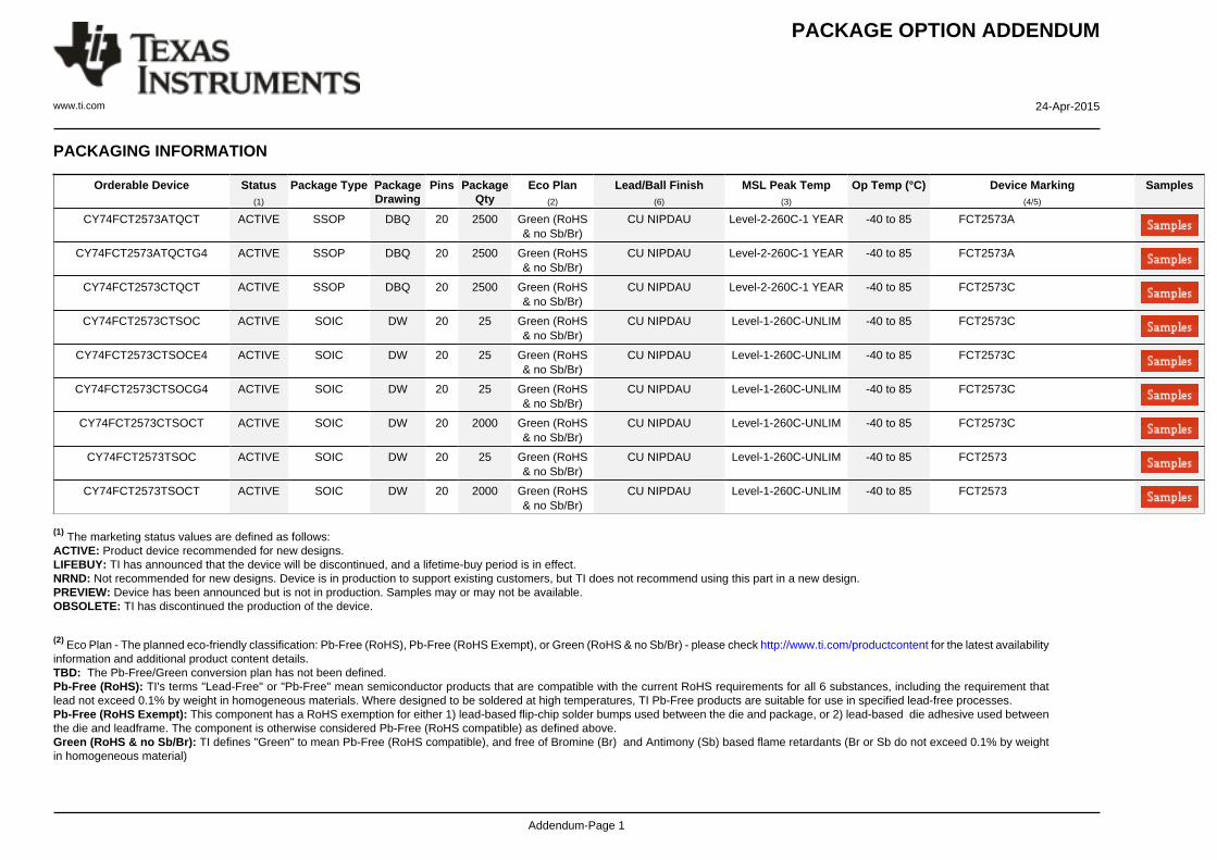
PACKAGE OPTION ADDENDUM
www.ti.com 24-Apr-2015
Addendum-Page 1
PACKAGING INFORMATION
Orderable Device Status(1)
Package Type PackageDrawing
Pins PackageQty
Eco Plan(2)
Lead/Ball Finish(6)
MSL Peak Temp(3)
Op Temp (°C) Device Marking(4/5)
Samples
CY74FCT2573ATQCT ACTIVE SSOP DBQ 20 2500 Green (RoHS& no Sb/Br)
CU NIPDAU Level-2-260C-1 YEAR -40 to 85 FCT2573A
CY74FCT2573ATQCTG4 ACTIVE SSOP DBQ 20 2500 Green (RoHS& no Sb/Br)
CU NIPDAU Level-2-260C-1 YEAR -40 to 85 FCT2573A
CY74FCT2573CTQCT ACTIVE SSOP DBQ 20 2500 Green (RoHS& no Sb/Br)
CU NIPDAU Level-2-260C-1 YEAR -40 to 85 FCT2573C
CY74FCT2573CTSOC ACTIVE SOIC DW 20 25 Green (RoHS& no Sb/Br)
CU NIPDAU Level-1-260C-UNLIM -40 to 85 FCT2573C
CY74FCT2573CTSOCE4 ACTIVE SOIC DW 20 25 Green (RoHS& no Sb/Br)
CU NIPDAU Level-1-260C-UNLIM -40 to 85 FCT2573C
CY74FCT2573CTSOCG4 ACTIVE SOIC DW 20 25 Green (RoHS& no Sb/Br)
CU NIPDAU Level-1-260C-UNLIM -40 to 85 FCT2573C
CY74FCT2573CTSOCT ACTIVE SOIC DW 20 2000 Green (RoHS& no Sb/Br)
CU NIPDAU Level-1-260C-UNLIM -40 to 85 FCT2573C
CY74FCT2573TSOC ACTIVE SOIC DW 20 25 Green (RoHS& no Sb/Br)
CU NIPDAU Level-1-260C-UNLIM -40 to 85 FCT2573
CY74FCT2573TSOCT ACTIVE SOIC DW 20 2000 Green (RoHS& no Sb/Br)
CU NIPDAU Level-1-260C-UNLIM -40 to 85 FCT2573
(1) The marketing status values are defined as follows:ACTIVE: Product device recommended for new designs.LIFEBUY: TI has announced that the device will be discontinued, and a lifetime-buy period is in effect.NRND: Not recommended for new designs. Device is in production to support existing customers, but TI does not recommend using this part in a new design.PREVIEW: Device has been announced but is not in production. Samples may or may not be available.OBSOLETE: TI has discontinued the production of the device.
(2) Eco Plan - The planned eco-friendly classification: Pb-Free (RoHS), Pb-Free (RoHS Exempt), or Green (RoHS & no Sb/Br) - please check http://www.ti.com/productcontent for the latest availabilityinformation and additional product content details.TBD: The Pb-Free/Green conversion plan has not been defined.Pb-Free (RoHS): TI's terms "Lead-Free" or "Pb-Free" mean semiconductor products that are compatible with the current RoHS requirements for all 6 substances, including the requirement thatlead not exceed 0.1% by weight in homogeneous materials. Where designed to be soldered at high temperatures, TI Pb-Free products are suitable for use in specified lead-free processes.Pb-Free (RoHS Exempt): This component has a RoHS exemption for either 1) lead-based flip-chip solder bumps used between the die and package, or 2) lead-based die adhesive used betweenthe die and leadframe. The component is otherwise considered Pb-Free (RoHS compatible) as defined above.Green (RoHS & no Sb/Br): TI defines "Green" to mean Pb-Free (RoHS compatible), and free of Bromine (Br) and Antimony (Sb) based flame retardants (Br or Sb do not exceed 0.1% by weightin homogeneous material)
PACKAGE OPTION ADDENDUM
www.ti.com 24-Apr-2015
Addendum-Page 2
(3) MSL, Peak Temp. - The Moisture Sensitivity Level rating according to the JEDEC industry standard classifications, and peak solder temperature.
(4) There may be additional marking, which relates to the logo, the lot trace code information, or the environmental category on the device.
(5) Multiple Device Markings will be inside parentheses. Only one Device Marking contained in parentheses and separated by a "~" will appear on a device. If a line is indented then it is a continuationof the previous line and the two combined represent the entire Device Marking for that device.
(6) Lead/Ball Finish - Orderable Devices may have multiple material finish options. Finish options are separated by a vertical ruled line. Lead/Ball Finish values may wrap to two lines if the finishvalue exceeds the maximum column width.
Important Information and Disclaimer:The information provided on this page represents TI's knowledge and belief as of the date that it is provided. TI bases its knowledge and belief on informationprovided by third parties, and makes no representation or warranty as to the accuracy of such information. Efforts are underway to better integrate information from third parties. TI has taken andcontinues to take reasonable steps to provide representative and accurate information but may not have conducted destructive testing or chemical analysis on incoming materials and chemicals.TI and TI suppliers consider certain information to be proprietary, and thus CAS numbers and other limited information may not be available for release.
In no event shall TI's liability arising out of such information exceed the total purchase price of the TI part(s) at issue in this document sold by TI to Customer on an annual basis.
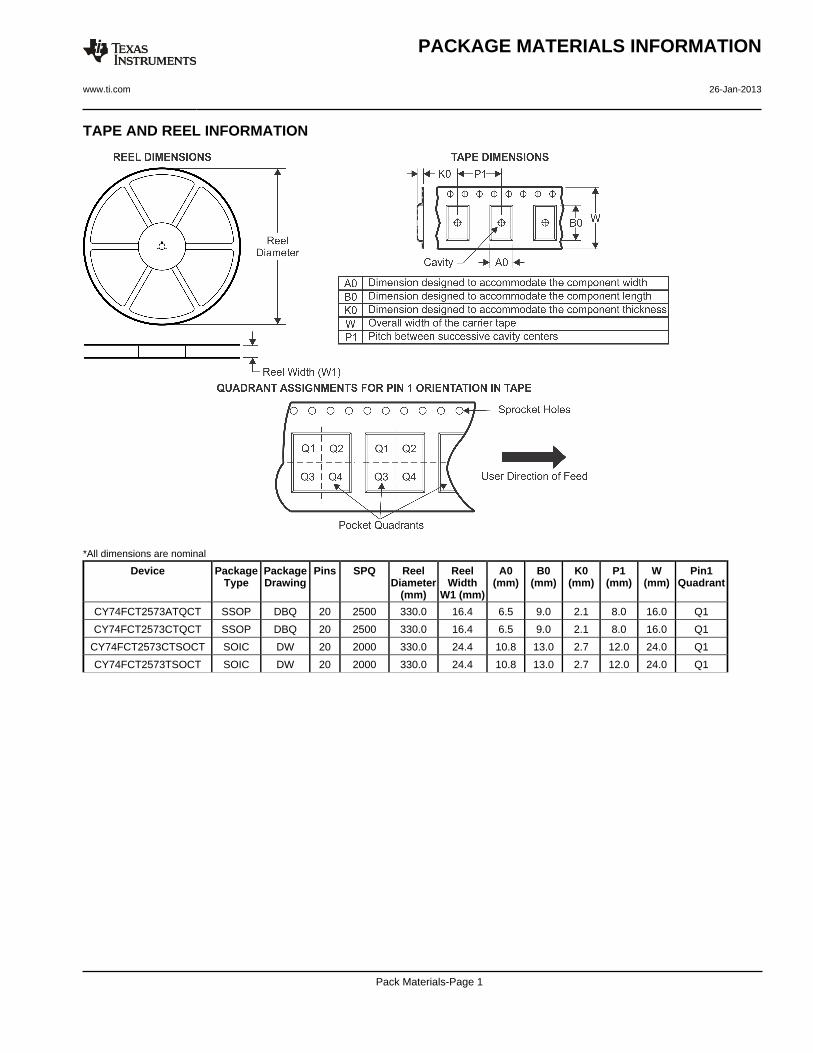
TAPE AND REEL INFORMATION
*All dimensions are nominal
Device PackageType
PackageDrawing
Pins SPQ ReelDiameter
(mm)
ReelWidth
W1 (mm)
A0(mm)
B0(mm)
K0(mm)
P1(mm)
W(mm)
Pin1Quadrant
CY74FCT2573ATQCT SSOP DBQ 20 2500 330.0 16.4 6.5 9.0 2.1 8.0 16.0 Q1
CY74FCT2573CTQCT SSOP DBQ 20 2500 330.0 16.4 6.5 9.0 2.1 8.0 16.0 Q1
CY74FCT2573CTSOCT SOIC DW 20 2000 330.0 24.4 10.8 13.0 2.7 12.0 24.0 Q1
CY74FCT2573TSOCT SOIC DW 20 2000 330.0 24.4 10.8 13.0 2.7 12.0 24.0 Q1
PACKAGE MATERIALS INFORMATION
www.ti.com 26-Jan-2013
Pack Materials-Page 1
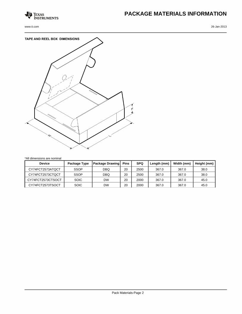
*All dimensions are nominal
Device Package Type Package Drawing Pins SPQ Length (mm) Width (mm) Height (mm)
CY74FCT2573ATQCT SSOP DBQ 20 2500 367.0 367.0 38.0
CY74FCT2573CTQCT SSOP DBQ 20 2500 367.0 367.0 38.0
CY74FCT2573CTSOCT SOIC DW 20 2000 367.0 367.0 45.0
CY74FCT2573TSOCT SOIC DW 20 2000 367.0 367.0 45.0
PACKAGE MATERIALS INFORMATION
www.ti.com 26-Jan-2013
Pack Materials-Page 2
www.ti.com
PACKAGE OUTLINE
C
TYP10.639.97
2.65 MAX
18X 1.27
20X 0.510.31
2X11.43
TYP0.330.10
0 - 80.30.1
0.25GAGE PLANE
1.270.40
A
NOTE 3
13.012.6
B 7.67.4
4220724/A 05/2016
SOIC - 2.65 mm max heightDW0020ASOIC
NOTES: 1. All linear dimensions are in millimeters. Dimensions in parenthesis are for reference only. Dimensioning and tolerancing per ASME Y14.5M. 2. This drawing is subject to change without notice. 3. This dimension does not include mold flash, protrusions, or gate burrs. Mold flash, protrusions, or gate burrs shall not exceed 0.15 mm per side. 4. This dimension does not include interlead flash. Interlead flash shall not exceed 0.43 mm per side.5. Reference JEDEC registration MS-013.
120
0.25 C A B
1110
PIN 1 IDAREA
NOTE 4
SEATING PLANE
0.1 C
SEE DETAIL A
DETAIL ATYPICAL
SCALE 1.200

www.ti.com
EXAMPLE BOARD LAYOUT
(9.3)
0.07 MAXALL AROUND
0.07 MINALL AROUND
20X (2)
20X (0.6)
18X (1.27)
(R )TYP
0.05
4220724/A 05/2016
SOIC - 2.65 mm max heightDW0020ASOIC
SYMM
SYMM
LAND PATTERN EXAMPLESCALE:6X
1
10 11
20
NOTES: (continued) 6. Publication IPC-7351 may have alternate designs. 7. Solder mask tolerances between and around signal pads can vary based on board fabrication site.
METALSOLDER MASKOPENING
NON SOLDER MASKDEFINED
SOLDER MASK DETAILS
SOLDER MASKOPENING
METAL UNDERSOLDER MASK
SOLDER MASKDEFINED
www.ti.com
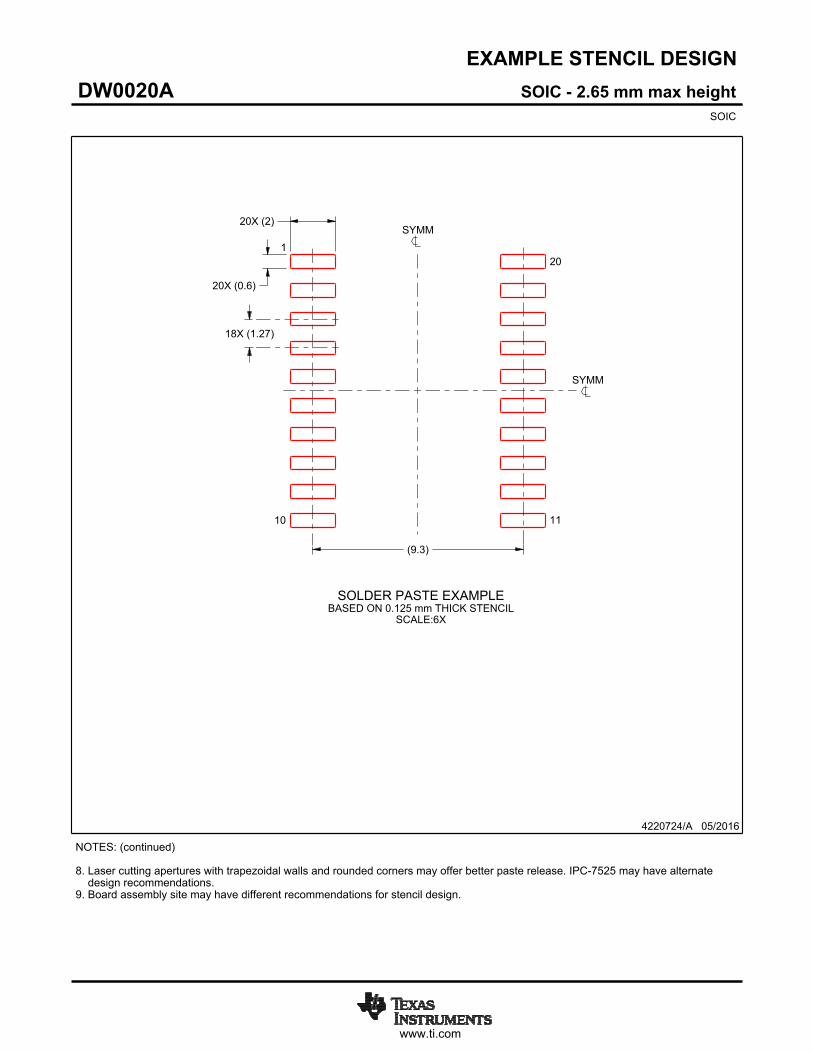
EXAMPLE STENCIL DESIGN
(9.3)
18X (1.27)
20X (0.6)
20X (2)
4220724/A 05/2016
SOIC - 2.65 mm max heightDW0020ASOIC
NOTES: (continued) 8. Laser cutting apertures with trapezoidal walls and rounded corners may offer better paste release. IPC-7525 may have alternate design recommendations. 9. Board assembly site may have different recommendations for stencil design.
SYMM
SYMM
1
10 11
20
SOLDER PASTE EXAMPLEBASED ON 0.125 mm THICK STENCIL
SCALE:6X
IMPORTANT NOTICE
Texas Instruments Incorporated (TI) reserves the right to make corrections, enhancements, improvements and other changes to itssemiconductor products and services per JESD46, latest issue, and to discontinue any product or service per JESD48, latest issue. Buyersshould obtain the latest relevant information before placing orders and should verify that such information is current and complete.TI’s published terms of sale for semiconductor products (http://www.ti.com/sc/docs/stdterms.htm) apply to the sale of packaged integratedcircuit products that TI has qualified and released to market. Additional terms may apply to the use or sale of other types of TI products andservices.Reproduction of significant portions of TI information in TI data sheets is permissible only if reproduction is without alteration and isaccompanied by all associated warranties, conditions, limitations, and notices. TI is not responsible or liable for such reproduceddocumentation. Information of third parties may be subject to additional restrictions. Resale of TI products or services with statementsdifferent from or beyond the parameters stated by TI for that product or service voids all express and any implied warranties for theassociated TI product or service and is an unfair and deceptive business practice. TI is not responsible or liable for any such statements.Buyers and others who are developing systems that incorporate TI products (collectively, “Designers”) understand and agree that Designersremain responsible for using their independent analysis, evaluation and judgment in designing their applications and that Designers havefull and exclusive responsibility to assure the safety of Designers' applications and compliance of their applications (and of all TI productsused in or for Designers’ applications) with all applicable regulations, laws and other applicable requirements. Designer represents that, withrespect to their applications, Designer has all the necessary expertise to create and implement safeguards that (1) anticipate dangerousconsequences of failures, (2) monitor failures and their consequences, and (3) lessen the likelihood of failures that might cause harm andtake appropriate actions. Designer agrees that prior to using or distributing any applications that include TI products, Designer willthoroughly test such applications and the functionality of such TI products as used in such applications.TI’s provision of technical, application or other design advice, quality characterization, reliability data or other services or information,including, but not limited to, reference designs and materials relating to evaluation modules, (collectively, “TI Resources”) are intended toassist designers who are developing applications that incorporate TI products; by downloading, accessing or using TI Resources in anyway, Designer (individually or, if Designer is acting on behalf of a company, Designer’s company) agrees to use any particular TI Resourcesolely for this purpose and subject to the terms of this Notice.TI’s provision of TI Resources does not expand or otherwise alter TI’s applicable published warranties or warranty disclaimers for TIproducts, and no additional obligations or liabilities arise from TI providing such TI Resources. TI reserves the right to make corrections,enhancements, improvements and other changes to its TI Resources. TI has not conducted any testing other than that specificallydescribed in the published documentation for a particular TI Resource.Designer is authorized to use, copy and modify any individual TI Resource only in connection with the development of applications thatinclude the TI product(s) identified in such TI Resource. NO OTHER LICENSE, EXPRESS OR IMPLIED, BY ESTOPPEL OR OTHERWISETO ANY OTHER TI INTELLECTUAL PROPERTY RIGHT, AND NO LICENSE TO ANY TECHNOLOGY OR INTELLECTUAL PROPERTYRIGHT OF TI OR ANY THIRD PARTY IS GRANTED HEREIN, including but not limited to any patent right, copyright, mask work right, orother intellectual property right relating to any combination, machine, or process in which TI products or services are used. Informationregarding or referencing third-party products or services does not constitute a license to use such products or services, or a warranty orendorsement thereof. Use of TI Resources may require a license from a third party under the patents or other intellectual property of thethird party, or a license from TI under the patents or other intellectual property of TI.TI RESOURCES ARE PROVIDED “AS IS” AND WITH ALL FAULTS. TI DISCLAIMS ALL OTHER WARRANTIES ORREPRESENTATIONS, EXPRESS OR IMPLIED, REGARDING RESOURCES OR USE THEREOF, INCLUDING BUT NOT LIMITED TOACCURACY OR COMPLETENESS, TITLE, ANY EPIDEMIC FAILURE WARRANTY AND ANY IMPLIED WARRANTIES OFMERCHANTABILITY, FITNESS FOR A PARTICULAR PURPOSE, AND NON-INFRINGEMENT OF ANY THIRD PARTY INTELLECTUALPROPERTY RIGHTS. TI SHALL NOT BE LIABLE FOR AND SHALL NOT DEFEND OR INDEMNIFY DESIGNER AGAINST ANY CLAIM,INCLUDING BUT NOT LIMITED TO ANY INFRINGEMENT CLAIM THAT RELATES TO OR IS BASED ON ANY COMBINATION OFPRODUCTS EVEN IF DESCRIBED IN TI RESOURCES OR OTHERWISE. IN NO EVENT SHALL TI BE LIABLE FOR ANY ACTUAL,DIRECT, SPECIAL, COLLATERAL, INDIRECT, PUNITIVE, INCIDENTAL, CONSEQUENTIAL OR EXEMPLARY DAMAGES INCONNECTION WITH OR ARISING OUT OF TI RESOURCES OR USE THEREOF, AND REGARDLESS OF WHETHER TI HAS BEENADVISED OF THE POSSIBILITY OF SUCH DAMAGES.Unless TI has explicitly designated an individual product as meeting the requirements of a particular industry standard (e.g., ISO/TS 16949and ISO 26262), TI is not responsible for any failure to meet such industry standard requirements.Where TI specifically promotes products as facilitating functional safety or as compliant with industry functional safety standards, suchproducts are intended to help enable customers to design and create their own applications that meet applicable functional safety standardsand requirements. Using products in an application does not by itself establish any safety features in the application. Designers mustensure compliance with safety-related requirements and standards applicable to their applications. Designer may not use any TI products inlife-critical medical equipment unless authorized officers of the parties have executed a special contract specifically governing such use.Life-critical medical equipment is medical equipment where failure of such equipment would cause serious bodily injury or death (e.g., lifesupport, pacemakers, defibrillators, heart pumps, neurostimulators, and implantables). Such equipment includes, without limitation, allmedical devices identified by the U.S. Food and Drug Administration as Class III devices and equivalent classifications outside the U.S.TI may expressly designate certain products as completing a particular qualification (e.g., Q100, Military Grade, or Enhanced Product).Designers agree that it has the necessary expertise to select the product with the appropriate qualification designation for their applicationsand that proper product selection is at Designers’ own risk. Designers are solely responsible for compliance with all legal and regulatoryrequirements in connection with such selection.Designer will fully indemnify TI and its representatives against any damages, costs, losses, and/or liabilities arising out of Designer’s non-compliance with the terms and provisions of this Notice.
Mailing Address: Texas Instruments, Post Office Box 655303, Dallas, Texas 75265Copyright © 2017, Texas Instruments Incorporated