8-Bit To 9-Bit Parity Bus Transceivers (Rev. F Sheets/Texas...SN54ABT853, SN74ABT853 8-BIT TO 9-BIT...
21
SN54ABT853, SN74ABT853 8-BIT TO 9-BIT PARITY BUS TRANSCEIVERS SCBS198F – FEBRUARY 1991 – REVISED OCTOBER 1997 1 POST OFFICE BOX 655303 • DALLAS, TEXAS 75265 State-of-the-Art EPIC-ΙΙB BiCMOS Design Significantly Reduces Power Dissipation ESD Protection Exceeds 2000 V Per MIL-STD-883, Method 3015; Exceeds 200 V Using Machine Model (C = 200 pF, R = 0) Latch-Up Performance Exceeds 500 mA Per JESD 17 Typical V OLP (Output Ground Bounce) < 1 V at V CC = 5 V, T A = 25°C High-Drive Outputs (–32-mA I OH , 64-mA I OL ) High-Impedance State During Power Up and Power Down Parity-Error Flag With Parity Generator/Checker Latch for Storage of Parity-Error Flag Package Options Include Plastic Small-Outline (DW), Shrink Small-Outline (DB), and Thin Shrink Small-Outline (PW) Packages, Ceramic Chip Carriers (FK), Ceramic Flat (W) Package, and Plastic (NT) and Ceramic (JT) DIPs description The ’ABT853 8-bit to 9-bit parity transceivers are designed for communication between data buses. When data is transmitted from the A bus to the B bus, a parity bit is generated. When data is transmitted from the B bus to the A bus with its corresponding parity bit, the open-collector parity-error (ERR ) output indicates whether or not an error in the B data has occurred. The output-enable (OEA and OEB ) inputs can be used to disable the device so that the buses are effectively isolated. The ’ABT853 transceivers provide true data at their outputs. A 9-bit parity generator/checker generates a parity-odd (PARITY) output and monitors the parity of the I/O ports with the ERR flag. The parity-error output can be passed, sampled, stored, or cleared from the latch using the latch-enable (LE ) and clear (CLR ) control inputs. When both OEA and OEB are low, data is transferred from the A bus to the B bus and inverted parity is generated. Inverted parity is a forced error condition that gives the designer more system diagnostic capability. When V CC is between 0 and 2.1 V, the device is in the high-impedance state during power up or power down. However, to ensure the high-impedance state above 2.1 V, OE should be tied to V CC through a pullup resistor; the minimum value of the resistor is determined by the current-sinking capability of the driver. Copyright 1997, Texas Instruments Incorporated PRODUCTION DATA information is current as of publication date. Products conform to specifications per the terms of Texas Instruments standard warranty. Production processing does not necessarily include testing of all parameters. EPIC-ΙΙB is a trademark of Texas Instruments Incorporated. Please be aware that an important notice concerning availability, standard warranty, and use in critical applications of Texas Instruments semiconductor products and disclaimers thereto appears at the end of this data sheet. 1 2 3 4 5 6 7 8 9 10 11 12 24 23 22 21 20 19 18 17 16 15 14 13 OEA A1 A2 A3 A4 A5 A6 A7 A8 ERR CLR GND V CC B1 B2 B3 B4 B5 B6 B7 B8 PARITY OEB LE SN54ABT853 . . . JT OR W PACKAGE SN74ABT853. . . DB, DW, NT, OR PW PACKAGE (TOP VIEW) 3 2 1 28 27 12 13 5 6 7 8 9 10 11 25 24 23 22 21 20 19 B3 B4 B5 NC B6 B7 B8 A3 A4 A5 NC A6 A7 A8 4 26 14 15 16 17 18 ERR CLR GND NC LE OEB PARITY A2 A1 OEA NC B1 B2 SN54ABT853 . . . FK PACKAGE (TOP VIEW) V CC NC – No internal connection
Transcript of 8-Bit To 9-Bit Parity Bus Transceivers (Rev. F Sheets/Texas...SN54ABT853, SN74ABT853 8-BIT TO 9-BIT...

SN54ABT853, SN74ABT8538-BIT TO 9-BIT PARITY BUS TRANSCEIVERS
SCBS198F – FEBRUARY 1991 – REVISED OCTOBER 1997
1POST OFFICE BOX 655303 • DALLAS, TEXAS 75265
State-of-the-Art EPIC-ΙΙB BiCMOS DesignSignificantly Reduces Power Dissipation
ESD Protection Exceeds 2000 V PerMIL-STD-883, Method 3015; Exceeds 200 VUsing Machine Model (C = 200 pF, R = 0)
Latch-Up Performance Exceeds 500 mA PerJESD 17
Typical V OLP (Output Ground Bounce)< 1 V at VCC = 5 V, TA = 25°C
High-Drive Outputs (–32-mA I OH, 64-mA IOL)
High-Impedance State During Power Upand Power Down
Parity-Error Flag With ParityGenerator/Checker
Latch for Storage of Parity-Error Flag
Package Options Include PlasticSmall-Outline (DW), Shrink Small-Outline(DB), and Thin Shrink Small-Outline (PW)Packages, Ceramic Chip Carriers (FK),Ceramic Flat (W) Package, and Plastic (NT)and Ceramic (JT) DIPs
description
The ’ABT853 8-bit to 9-bit parity transceivers aredesigned for communication between data buses.When data is transmitted from the A bus to theB bus, a parity bit is generated. When data istransmitted from the B bus to the A bus with itscorresponding parity bit, the open-collectorparity-error (ERR) output indicates whether or notan error in the B data has occurred. Theoutput-enable (OEA and OEB) inputs can be usedto disable the device so that the buses areeffectively isolated. The ’ABT853 transceiversprovide true data at their outputs.
A 9-bit parity generator/checker generates a parity-odd (PARITY) output and monitors the parity of the I/O portswith the ERR flag. The parity-error output can be passed, sampled, stored, or cleared from the latch using thelatch-enable (LE) and clear (CLR) control inputs. When both OEA and OEB are low, data is transferred fromthe A bus to the B bus and inverted parity is generated. Inverted parity is a forced error condition that gives thedesigner more system diagnostic capability.
When VCC is between 0 and 2.1 V, the device is in the high-impedance state during power up or power down.However, to ensure the high-impedance state above 2.1 V, OE should be tied to VCC through a pullup resistor;the minimum value of the resistor is determined by the current-sinking capability of the driver.
Copyright 1997, Texas Instruments IncorporatedPRODUCTION DATA information is current as of publication date.Products conform to specifications per the terms of Texas Instrumentsstandard warranty. Production processing does not necessarily includetesting of all parameters.
EPIC-ΙΙB is a trademark of Texas Instruments Incorporated.
Please be aware that an important notice concerning availability, standard warranty, and use in critical applications ofTexas Instruments semiconductor products and disclaimers thereto appears at the end of this data sheet.
1
2
3
4
5
6
7
8
9
10
11
12
24
23
22
21
20
19
18
17
16
15
14
13
OEAA1A2A3A4A5A6A7A8
ERRCLRGND
VCCB1B2B3B4B5B6B7B8PARITYOEBLE
SN54ABT853 . . . JT OR W PACKAGESN74ABT853 . . . DB, DW, NT, OR PW PACKAGE
(TOP VIEW)
3 2 1 28 27
12 13
5
6
7
8
9
10
11
25
24
23
22
21
20
19
B3B4B5NCB6B7B8
A3A4A5NCA6A7A8
4 26
14 15 16 17 18
ER
R
CLR
GN
DN
C LEO
EB
PA
RIT
Y
A2
A1
OE
AN
C
B1
B2
SN54ABT853 . . . FK PACKAGE(TOP VIEW)
VC
C
NC – No internal connection
SN54ABT853, SN74ABT8538-BIT TO 9-BIT PARITY BUS TRANSCEIVERS
SCBS198F – FEBRUARY 1991 – REVISED OCTOBER 1997
2 POST OFFICE BOX 655303 • DALLAS, TEXAS 75265
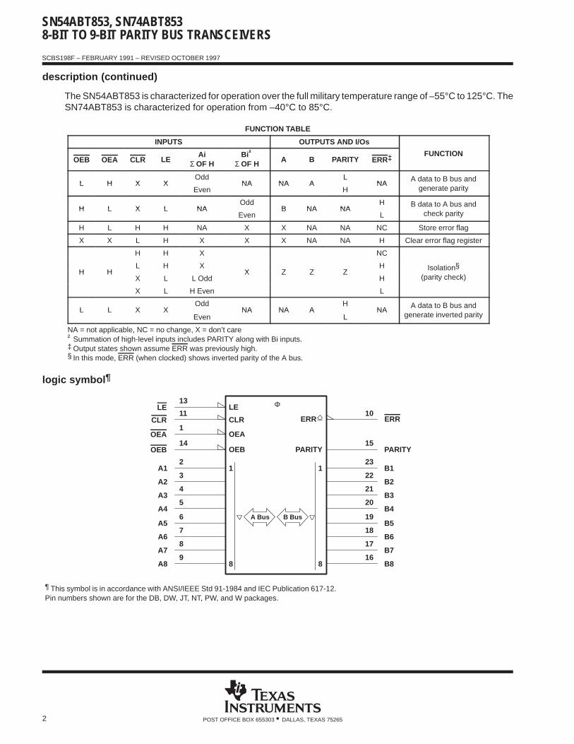
description (continued)
The SN54ABT853 is characterized for operation over the full military temperature range of –55°C to 125°C. TheSN74ABT853 is characterized for operation from –40°C to 85°C.
FUNCTION TABLE
INPUTS OUTPUTS AND I/Os
OEB OEA CLR LEAi
Σ OF HBi†
Σ OF H A B PARITY ERR‡ FUNCTION
L H X XOdd
NA NA AL
NAA data to B bus and
L H X XEven
NA NA AH
NAgenerate parity
H L X L NAOdd
B NA NAH B data to A bus and
H L X L NAEven
B NA NAL check parity
H L H H NA X X NA NA NC Store error flag
X X L H X X X NA NA H Clear error flag register
H H X NC
§H H
L H XX Z Z Z
H Isolation§H H
X L L OddX Z Z Z
H (parity check)
X L H Even L
L L X XOdd
NA NA AH
NAA data to B bus and
L L X XEven
NA NA AL
NAgenerate inverted parity
NA = not applicable, NC = no change, X = don’t care† Summation of high-level inputs includes PARITY along with Bi inputs.‡ Output states shown assume ERR was previously high.§ In this mode, ERR (when clocked) shows inverted parity of the A bus.
logic symbol ¶
ERRCLR
OEA
OEB
CLR11
12
A13
A24
A35
A4
10
PARITY15
PARITY
B519
B618
B717
B816
8
OEA1
OEB14
6A5
7A6
8A7
89
A8
B123
1
B222
B321
B420
ERR
Φ
A Bus B Bus
LE LE13
¶ This symbol is in accordance with ANSI/IEEE Std 91-1984 and IEC Publication 617-12.Pin numbers shown are for the DB, DW, JT, NT, PW, and W packages.

SN54ABT853, SN74ABT8538-BIT TO 9-BIT PARITY BUS TRANSCEIVERS
SCBS198F – FEBRUARY 1991 – REVISED OCTOBER 1997
3POST OFFICE BOX 655303 • DALLAS, TEXAS 75265
logic diagram (positive logic)
PARITY
ERR
CLR
B1–B8A1–A8
LE
OEA
OEB
EN
EN
8x
8x
MUX1
1
G1
1
12k
P
8
9
8
8
8
8
Pin numbers shown are for the DB, DW, JT, NT, PW, and W packages.
2–9
14
1
13
11
23–16
15
10
ERROR-FLAG FUNCTION TABLE
INPUTSINTERNALTO DEVICE
OUTPUTPRESTATE OUTPUT
ERR FUNCTIONCLR LE POINT P ERRN–1†
ERR
L LL
XL
PassL LH
XH
Pass
L X L
H L X L L Sample
H H H
L H X X H Clear
H H XL L
StoreH H XH H
Store
† The state of ERR before changes at CLR, LE, or point P
SN54ABT853, SN74ABT8538-BIT TO 9-BIT PARITY BUS TRANSCEIVERS
SCBS198F – FEBRUARY 1991 – REVISED OCTOBER 1997
4 POST OFFICE BOX 655303 • DALLAS, TEXAS 75265
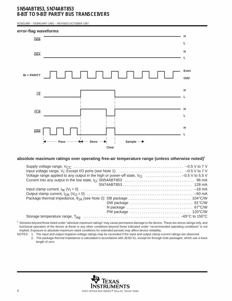
error-flag waveforms
ERR
CLR
LE
OEA
OEB
Bi + PARITY
H
L
H
L
Even
Odd
H
L
H
L
H
L
Pass Store Sample
Clear
absolute maximum ratings over operating free-air temperature range (unless otherwise noted) †
Supply voltage range, VCC –0.5 V to 7 V. . . . . . . . . . . . . . . . . . . . . . . . . . . . . . . . . . . . . . . . . . . . . . . . . . . . . . . . . . Input voltage range, VI: Except I/O ports (see Note 1) –0.5 V to 7 V. . . . . . . . . . . . . . . . . . . . . . . . . . . . . . . . . . Voltage range applied to any output in the high or power-off state, VO –0.5 V to 5.5 V. . . . . . . . . . . . . . . . . . . Current into any output in the low state, IO: SN54ABT853 96 mA. . . . . . . . . . . . . . . . . . . . . . . . . . . . . . . . . . . . .
SN74ABT853 128 mA. . . . . . . . . . . . . . . . . . . . . . . . . . . . . . . . . . . . . Input clamp current, IIK (VI < 0) –18 mA. . . . . . . . . . . . . . . . . . . . . . . . . . . . . . . . . . . . . . . . . . . . . . . . . . . . . . . . . . . Output clamp current, IOK (VO < 0) –50 mA. . . . . . . . . . . . . . . . . . . . . . . . . . . . . . . . . . . . . . . . . . . . . . . . . . . . . . . . Package thermal impedance, θJA (see Note 2): DB package 104°C/W. . . . . . . . . . . . . . . . . . . . . . . . . . . . . . . . .
DW package 81°C/W. . . . . . . . . . . . . . . . . . . . . . . . . . . . . . . . . N package 67°C/W. . . . . . . . . . . . . . . . . . . . . . . . . . . . . . . . . . . PW package 120°C/W. . . . . . . . . . . . . . . . . . . . . . . . . . . . . . . .
Storage temperature range, Tstg –65°C to 150°C. . . . . . . . . . . . . . . . . . . . . . . . . . . . . . . . . . . . . . . . . . . . . . . . . . .
† Stresses beyond those listed under “absolute maximum ratings” may cause permanent damage to the device. These are stress ratings only, andfunctional operation of the device at these or any other conditions beyond those indicated under “recommended operating conditions” is notimplied. Exposure to absolute-maximum-rated conditions for extended periods may affect device reliability.
NOTES: 1. The input and output negative-voltage ratings may be exceeded if the input and output clamp-current ratings are observed.2. The package thermal impedance is calculated in accordance with JESD 51, except for through-hole packages, which use a trace
length of zero.

SN54ABT853, SN74ABT8538-BIT TO 9-BIT PARITY BUS TRANSCEIVERS
SCBS198F – FEBRUARY 1991 – REVISED OCTOBER 1997
5POST OFFICE BOX 655303 • DALLAS, TEXAS 75265
recommended operating conditions (see Note 3)
SN54ABT853 SN74ABT853UNIT
MIN MAX MIN MAXUNIT
VCC Supply voltage 4.5 5.5 4.5 5.5 V
VIH High-level input voltage 2 2 V
VIL Low-level input voltage 0.8 0.8 V
VI Input voltage 0 VCC 0 VCC V
VOH High-level output voltage ERR 5.5 5.5 V
IOH High-level output current Except ERR –24 –32 mA
IOL Low-level output current 48 64 mA
∆t/∆v Input transition rise or fall rate Outputs enabled 10 10 ns/V
∆t/∆VCC Power-up ramp rate 200 200 µs/V
TA Operating free-air temperature –55 125 –40 85 °C
NOTE 3: Unused pins (input or I/O) must be held high or low to prevent them from floating.
SN54ABT853, SN74ABT8538-BIT TO 9-BIT PARITY BUS TRANSCEIVERS
SCBS198F – FEBRUARY 1991 – REVISED OCTOBER 1997
6 POST OFFICE BOX 655303 • DALLAS, TEXAS 75265
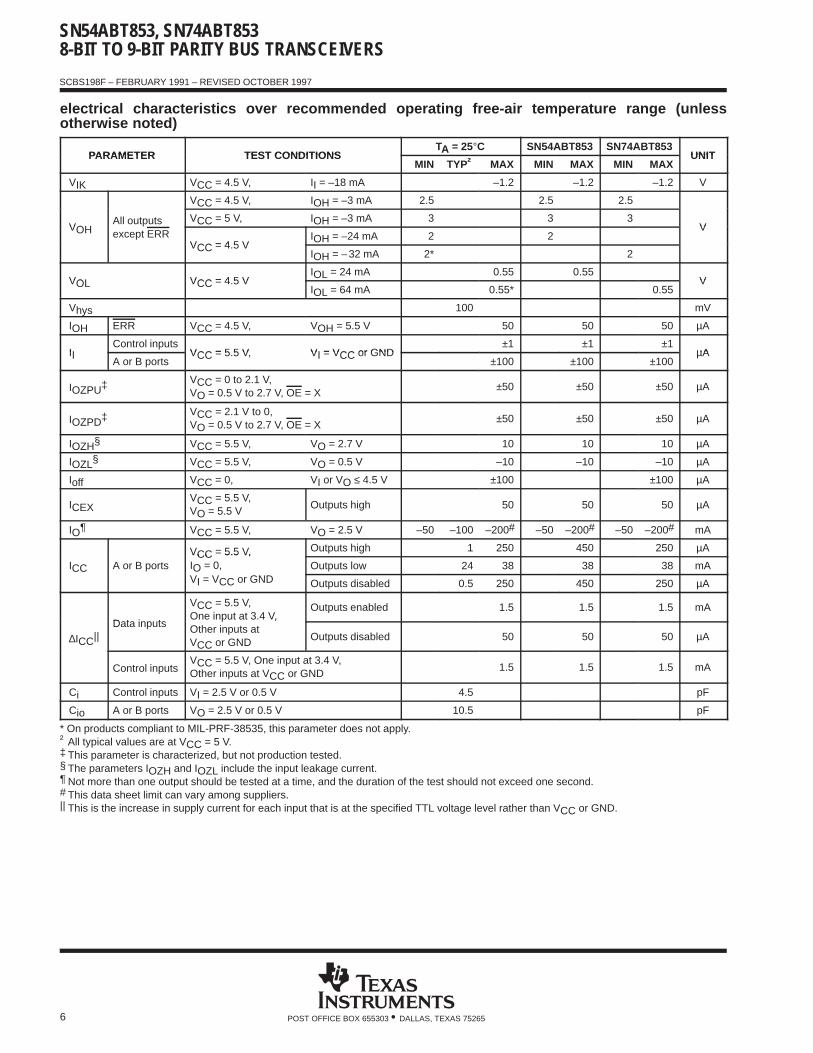
electrical characteristics over recommended operating free-air temperature range (unlessotherwise noted)
PARAMETER TEST CONDITIONSTA = 25°C SN54ABT853 SN74ABT853
UNITPARAMETER TEST CONDITIONSMIN TYP† MAX MIN MAX MIN MAX
UNIT
VIK VCC = 4.5 V, II = –18 mA –1.2 –1.2 –1.2 V
VCC = 4.5 V, IOH = –3 mA 2.5 2.5 2.5
VOHAll outputs VCC = 5 V, IOH = –3 mA 3 3 3
VVOH except ERRVCC = 4 5 V
IOH = –24 mA 2 2V
VCC = 4.5 VIOH = –32 mA 2* 2
VOL VCC = 4 5 VIOL = 24 mA 0.55 0.55
VVOL VCC = 4.5 VIOL = 64 mA 0.55* 0.55
V
Vhys 100 mV
IOH ERR VCC = 4.5 V, VOH = 5.5 V 50 50 50 µA
IIControl inputs
VCC = 5 5 V VI = VCC or GND±1 ±1 ±1
µAIIA or B ports
VCC = 5.5 V, VI = VCC or GND±100 ±100 ±100
µA
IOZPU‡ VCC = 0 to 2.1 V,VO = 0.5 V to 2.7 V, OE = X
±50 ±50 ±50 µA
IOZPD‡ VCC = 2.1 V to 0,VO = 0.5 V to 2.7 V, OE = X
±50 ±50 ±50 µA
IOZH§ VCC = 5.5 V, VO = 2.7 V 10 10 10 µA
IOZL§ VCC = 5.5 V, VO = 0.5 V –10 –10 –10 µA
Ioff VCC = 0, VI or VO ≤ 4.5 V ±100 ±100 µA
ICEXVCC = 5.5 V,VO = 5.5 V
Outputs high 50 50 50 µA
IO¶ VCC = 5.5 V, VO = 2.5 V –50 –100 –200# –50 –200# –50 –200# mA
VCC = 5.5 V, Outputs high 1 250 450 250 µA
ICC A or B portsVCC 5.5 V,IO = 0, Outputs low 24 38 38 38 mAVI = VCC or GND Outputs disabled 0.5 250 450 250 µA
||Data inp ts
VCC = 5.5 V,One input at 3.4 V,
Outputs enabled 1.5 1.5 1.5 mA
∆ICC||Data inputs
,Other inputs atVCC or GND Outputs disabled 50 50 50 µA
Control inputsVCC = 5.5 V, One input at 3.4 V,Other inputs at VCC or GND
1.5 1.5 1.5 mA
Ci Control inputs VI = 2.5 V or 0.5 V 4.5 pF
Cio A or B ports VO = 2.5 V or 0.5 V 10.5 pF
* On products compliant to MIL-PRF-38535, this parameter does not apply.† All typical values are at VCC = 5 V.‡ This parameter is characterized, but not production tested.§ The parameters IOZH and IOZL include the input leakage current.¶ Not more than one output should be tested at a time, and the duration of the test should not exceed one second.# This data sheet limit can vary among suppliers.|| This is the increase in supply current for each input that is at the specified TTL voltage level rather than VCC or GND.

SN54ABT853, SN74ABT8538-BIT TO 9-BIT PARITY BUS TRANSCEIVERS
SCBS198F – FEBRUARY 1991 – REVISED OCTOBER 1997
7POST OFFICE BOX 655303 • DALLAS, TEXAS 75265
timing requirements over recommended ranges of supply voltage and operating free-airtemperature (unless otherwise noted) (see Figure 1)
VCC = 5 V,TA = 25°C SN54ABT853 SN74ABT853
UNITMIN MAX MIN MAX MIN MAX
t Pulse durationLE high or low 3.5 3.5 3.5
nstw Pulse durationCLR low 4 4 4
ns
t Setup timeB or PARITY before LE↓ 9.4† 10.2 9.4†
nstsu Setup timeCLR before LE↓ 2 2 2
ns
th Hold timeB or PARITY after LE↓ 0 0 0
nsth Hold timeCLR after LE↓ 3 3 3
ns
† This data sheet limit can vary among suppliers.
switching characteristics over recommended ranges of supply voltage and operating free-airtemperature (unless otherwise noted) (see Figure 1)
PARAMETERFROM
(INPUT)TO
(OUTPUT)
VCC = 5 V,TA = 25°C SN54ABT853 SN74ABT853
UNIT(INPUT) (OUTPUT)MIN TYP MAX MIN MAX MIN MAX
tPLHA or B B or A
1.2 4.8 1.2 6.4 1.2 5.3ns
tPHLA or B B or A
1 4.8† 1 5.4 1 5.3†ns
tPLHA PARITY
2.1 9.5 2.1 13.3 2.1 11.2ns
tPHLA PARITY
2.5 9.7 2.5 11 2.5 11ns
tPLHOE PARITY
1.8 8.5 1.8 13.6 1.8 10.5ns
tPHLOE PARITY
2.3 8.6 2.3 11.7 2.3 10ns
tPLH CLR ERR 1 5.5 1 6.3 1 6.2 ns
tPLHLE ERR
1.8 5.1 1.8 6.1 1.8 6ns
tPHLLE ERR
1† 5.8 1† 6.7 1 6.6ns
tPLHB or PARITY ERR
2 10.1 2 11.8 2 11.7ns
tPHLB or PARITY ERR
2.2† 11.5 2.2† 12.9 2.2† 12.8ns
tPZHOE A or B or PARITY
1 5.8† 1 8.8 1 6.7†ns
tPZLOE A or B or PARITY
1.5† 5.8 1.5† 9.8 1.5† 6.7ns
tPHZOE A or B or PARITY
1.8† 7.3 1.8† 9.5 1.8† 7.9ns
tPLZOE A or B or PARITY
2.1† 7.2 2.1† 8.2 2.1† 8.1ns
† This data sheet limit can vary among suppliers.
SN54ABT853, SN74ABT8538-BIT TO 9-BIT PARITY BUS TRANSCEIVERS
SCBS198F – FEBRUARY 1991 – REVISED OCTOBER 1997
8 POST OFFICE BOX 655303 • DALLAS, TEXAS 75265
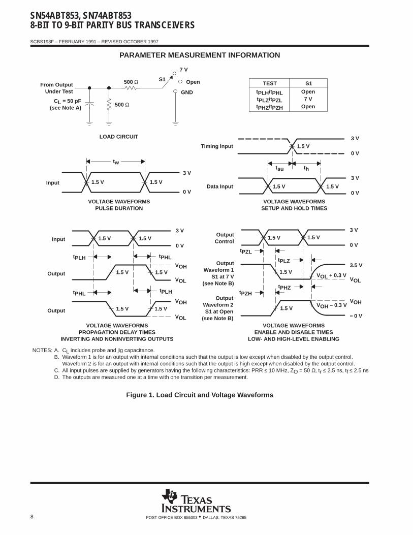
PARAMETER MEASUREMENT INFORMATION
From Output Under Test
CL = 50 pF(see Note A)
LOAD CIRCUIT
S1
7 V
Open
GND
500 Ω
500 Ω
tPLH/tPHLtPLZ/tPZLtPHZ/tPZH
Open7 V
Open
TEST S1
1.5 V
thtsu
Data Input
Timing Input 1.5 V3 V
0 V
1.5 V 1.5 V
3 V
0 V
3 V
0 V
1.5 V 1.5 V
tw
Input
VOLTAGE WAVEFORMSSETUP AND HOLD TIMES
VOLTAGE WAVEFORMSPROPAGATION DELAY TIMES
INVERTING AND NONINVERTING OUTPUTS
VOLTAGE WAVEFORMSPULSE DURATION
tPLH
tPHL
tPHL
tPLH
VOH
VOH
VOL
VOL
1.5 V 1.5 V3 V
0 V
1.5 V1.5 V
Input
1.5 V
OutputControl
OutputWaveform 1
S1 at 7 V(see Note B)
OutputWaveform 2S1 at Open
(see Note B)
VOL
VOH
tPZL
tPZH
tPLZ
tPHZ
1.5 V1.5 V
3.5 V
0 V
1.5 VVOL + 0.3 V
1.5 V VOH – 0.3 V
≈ 0 V
3 V
VOLTAGE WAVEFORMSENABLE AND DISABLE TIMES
LOW- AND HIGH-LEVEL ENABLING
Output
Output
NOTES: A. CL includes probe and jig capacitance.B. Waveform 1 is for an output with internal conditions such that the output is low except when disabled by the output control.
Waveform 2 is for an output with internal conditions such that the output is high except when disabled by the output control.C. All input pulses are supplied by generators having the following characteristics: PRR ≤ 10 MHz, ZO = 50 Ω, tr ≤ 2.5 ns, tf ≤ 2.5 ns.D. The outputs are measured one at a time with one transition per measurement.
Figure 1. Load Circuit and Voltage Waveforms

PACKAGING INFORMATION
Orderable Device Status (1) PackageType
PackageDrawing
Pins PackageQty
Eco Plan (2) Lead/Ball Finish MSL Peak Temp (3)
5962-9674601Q3A ACTIVE LCCC FK 28 1 TBD POST-PLATE N / A for Pkg Type
5962-9674601QKA ACTIVE CFP W 24 1 TBD A42 N / A for Pkg Type
5962-9674601QLA ACTIVE CDIP JT 24 1 TBD A42 N / A for Pkg Type
SN74ABT853DBLE OBSOLETE SSOP DB 24 TBD Call TI Call TI
SN74ABT853DBRE4 ACTIVE SSOP DB 24 TBD Call TI Call TI
SN74ABT853DBRG4 ACTIVE SSOP DB 24 TBD Call TI Call TI
SN74ABT853DW ACTIVE SOIC DW 24 25 Green (RoHS &no Sb/Br)
CU NIPDAU Level-1-260C-UNLIM
SN74ABT853DWE4 ACTIVE SOIC DW 24 25 Green (RoHS &no Sb/Br)
CU NIPDAU Level-1-260C-UNLIM
SN74ABT853DWG4 ACTIVE SOIC DW 24 25 Green (RoHS &no Sb/Br)
CU NIPDAU Level-1-260C-UNLIM
SN74ABT853DWR ACTIVE SOIC DW 24 2000 Green (RoHS &no Sb/Br)
CU NIPDAU Level-1-260C-UNLIM
SN74ABT853DWRE4 ACTIVE SOIC DW 24 2000 Green (RoHS &no Sb/Br)
CU NIPDAU Level-1-260C-UNLIM
SN74ABT853DWRG4 ACTIVE SOIC DW 24 2000 Green (RoHS &no Sb/Br)
CU NIPDAU Level-1-260C-UNLIM
SN74ABT853NSRE4 ACTIVE SO NS 24 TBD Call TI Call TI
SN74ABT853NSRG4 ACTIVE SO NS 24 TBD Call TI Call TI
SN74ABT853NT ACTIVE PDIP NT 24 15 Pb-Free(RoHS)
CU NIPDAU N / A for Pkg Type
SN74ABT853NTE4 ACTIVE PDIP NT 24 15 Pb-Free(RoHS)
CU NIPDAU N / A for Pkg Type
SN74ABT853PWE4 ACTIVE TSSOP PW 24 TBD Call TI Call TI
SN74ABT853PWG4 ACTIVE TSSOP PW 24 TBD Call TI Call TI
SN74ABT853PWLE OBSOLETE TSSOP PW 24 TBD Call TI Call TI
SN74ABT853PWRE4 ACTIVE TSSOP PW 24 TBD Call TI Call TI
SN74ABT853PWRG4 ACTIVE TSSOP PW 24 TBD Call TI Call TI
SNJ54ABT853FK ACTIVE LCCC FK 28 1 TBD POST-PLATE N / A for Pkg Type
SNJ54ABT853JT ACTIVE CDIP JT 24 1 TBD A42 N / A for Pkg Type
SNJ54ABT853W ACTIVE CFP W 24 1 TBD A42 N / A for Pkg Type
(1) The marketing status values are defined as follows:ACTIVE: Product device recommended for new designs.LIFEBUY: TI has announced that the device will be discontinued, and a lifetime-buy period is in effect.NRND: Not recommended for new designs. Device is in production to support existing customers, but TI does not recommend using this part ina new design.PREVIEW: Device has been announced but is not in production. Samples may or may not be available.OBSOLETE: TI has discontinued the production of the device.
(2) Eco Plan - The planned eco-friendly classification: Pb-Free (RoHS), Pb-Free (RoHS Exempt), or Green (RoHS & no Sb/Br) - please checkhttp://www.ti.com/productcontent for the latest availability information and additional product content details.TBD: The Pb-Free/Green conversion plan has not been defined.Pb-Free (RoHS): TI's terms "Lead-Free" or "Pb-Free" mean semiconductor products that are compatible with the current RoHS requirementsfor all 6 substances, including the requirement that lead not exceed 0.1% by weight in homogeneous materials. Where designed to be solderedat high temperatures, TI Pb-Free products are suitable for use in specified lead-free processes.Pb-Free (RoHS Exempt): This component has a RoHS exemption for either 1) lead-based flip-chip solder bumps used between the die andpackage, or 2) lead-based die adhesive used between the die and leadframe. The component is otherwise considered Pb-Free (RoHS
PACKAGE OPTION ADDENDUM
www.ti.com 15-Oct-2009
Addendum-Page 1

compatible) as defined above.Green (RoHS & no Sb/Br): TI defines "Green" to mean Pb-Free (RoHS compatible), and free of Bromine (Br) and Antimony (Sb) based flameretardants (Br or Sb do not exceed 0.1% by weight in homogeneous material)
(3) MSL, Peak Temp. -- The Moisture Sensitivity Level rating according to the JEDEC industry standard classifications, and peak soldertemperature.
Important Information and Disclaimer:The information provided on this page represents TI's knowledge and belief as of the date that it isprovided. TI bases its knowledge and belief on information provided by third parties, and makes no representation or warranty as to theaccuracy of such information. Efforts are underway to better integrate information from third parties. TI has taken and continues to takereasonable steps to provide representative and accurate information but may not have conducted destructive testing or chemical analysis onincoming materials and chemicals. TI and TI suppliers consider certain information to be proprietary, and thus CAS numbers and other limitedinformation may not be available for release.
In no event shall TI's liability arising out of such information exceed the total purchase price of the TI part(s) at issue in this document sold by TIto Customer on an annual basis.
PACKAGE OPTION ADDENDUM
www.ti.com 15-Oct-2009
Addendum-Page 2

TAPE AND REEL INFORMATION
*All dimensions are nominal
Device PackageType
PackageDrawing
Pins SPQ ReelDiameter
(mm)
ReelWidth
W1 (mm)
A0(mm)
B0(mm)
K0(mm)
P1(mm)
W(mm)
Pin1Quadrant
SN74ABT853DWR SOIC DW 24 2000 330.0 24.4 10.75 15.7 2.7 12.0 24.0 Q1
PACKAGE MATERIALS INFORMATION
www.ti.com 29-Jul-2009
Pack Materials-Page 1

*All dimensions are nominal
Device Package Type Package Drawing Pins SPQ Length (mm) Width (mm) Height (mm)
SN74ABT853DWR SOIC DW 24 2000 346.0 346.0 41.0
PACKAGE MATERIALS INFORMATION
www.ti.com 29-Jul-2009
Pack Materials-Page 2
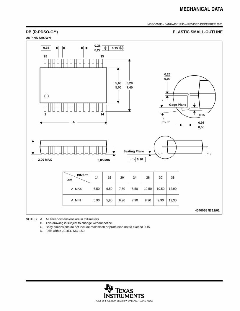
MECHANICAL DATA
MSSO002E – JANUARY 1995 – REVISED DECEMBER 2001
POST OFFICE BOX 655303 • DALLAS, TEXAS 75265
DB (R-PDSO-G**) PLASTIC SMALL-OUTLINE
4040065 /E 12/01
28 PINS SHOWN
Gage Plane
8,207,40
0,550,95
0,25
38
12,90
12,30
28
10,50
24
8,50
Seating Plane
9,907,90
30
10,50
9,90
0,38
5,605,00
15
0,22
14
A
28
1
2016
6,506,50
14
0,05 MIN
5,905,90
DIM
A MAX
A MIN
PINS **
2,00 MAX
6,90
7,50
0,65 M0,15
0°–8°
0,10
0,090,25
NOTES: A. All linear dimensions are in millimeters.B. This drawing is subject to change without notice.C. Body dimensions do not include mold flash or protrusion not to exceed 0,15.D. Falls within JEDEC MO-150

MECHANICAL DATA
MLCC006B – OCTOBER 1996
POST OFFICE BOX 655303 • DALLAS, TEXAS 75265
FK (S-CQCC-N**) LEADLESS CERAMIC CHIP CARRIER
4040140/D 10/96
28 TERMINAL SHOWN
B
0.358(9,09)
MAX
(11,63)
0.560(14,22)
0.560
0.458
0.858(21,8)
1.063(27,0)
(14,22)
ANO. OF
MINMAX
0.358
0.660
0.761
0.458
0.342(8,69)
MIN
(11,23)
(16,26)0.640
0.739
0.442
(9,09)
(11,63)
(16,76)
0.962
1.165
(23,83)0.938
(28,99)1.141
(24,43)
(29,59)
(19,32)(18,78)
**
20
28
52
44
68
84
0.020 (0,51)
TERMINALS
0.080 (2,03)0.064 (1,63)
(7,80)0.307
(10,31)0.406
(12,58)0.495
(12,58)0.495
(21,6)0.850
(26,6)1.047
0.045 (1,14)
0.045 (1,14)0.035 (0,89)
0.035 (0,89)
0.010 (0,25)
121314151618 17
11
10
8
9
7
5
432
0.020 (0,51)0.010 (0,25)
6
12826 27
19
21B SQ
A SQ22
23
24
25
20
0.055 (1,40)0.045 (1,14)
0.028 (0,71)0.022 (0,54)
0.050 (1,27)
NOTES: A. All linear dimensions are in inches (millimeters).B. This drawing is subject to change without notice.C. This package can be hermetically sealed with a metal lid.D. The terminals are gold plated.E. Falls within JEDEC MS-004


MECHANICAL DATA
MTSS001C – JANUARY 1995 – REVISED FEBRUARY 1999
POST OFFICE BOX 655303 • DALLAS, TEXAS 75265
PW (R-PDSO-G**) PLASTIC SMALL-OUTLINE PACKAGE14 PINS SHOWN
0,65 M0,10
0,10
0,25
0,500,75
0,15 NOM
Gage Plane
28
9,80
9,60
24
7,90
7,70
2016
6,60
6,40
4040064/F 01/97
0,30
6,606,20
8
0,19
4,304,50
7
0,15
14
A
1
1,20 MAX
14
5,10
4,90
8
3,10
2,90
A MAX
A MIN
DIMPINS **
0,05
4,90
5,10
Seating Plane
0°–8°
NOTES: A. All linear dimensions are in millimeters.B. This drawing is subject to change without notice.C. Body dimensions do not include mold flash or protrusion not to exceed 0,15.D. Falls within JEDEC MO-153


MECHANICAL DATA
MCFP007 – OCTOBER 1994
POST OFFICE BOX 655303 • DALLAS, TEXAS 75265
W (R-GDFP-F24) CERAMIC DUAL FLATPACK
4040180-5/B 03/95
1.115 (28,32)
0.090 (2,29)
0.375 (9,53)
0.019 (0,48)
0.030 (0,76)
0.045 (1,14)
0.006 (0,15)
0.045 (1,14)
0.015 (0,38)
0.015 (0,38)
0.026 (0,66)
0.004 (0,10)
0.340 (8,64)
0.840 (21,34)
1 24
0.360 (9,14)0.240 (6,10)
1312
Base and Seating Plane
30° TYP
0.360 (9,14)0.240 (6,10)
0.395 (10,03)0.360 (9,14)
0.640 (16,26)0.490 (12,45)
0.050 (1,27)
NOTES: A. All linear dimensions are in inches (millimeters).B. This drawing is subject to change without notice.C. This package can be hermetically sealed with a ceramic lid using glass frit.D. Falls within MIL-STD-1835 GDFP2-F24 and JEDEC MO-070ADE. Index point is provided on cap for terminal identification only.

MECHANICAL DATA
MCER004A – JANUARY 1995 – REVISED JANUARY 1997
POST OFFICE BOX 655303 • DALLAS, TEXAS 75265
JT (R-GDIP-T**) CERAMIC DUAL-IN-LINE24 LEADS SHOWN
4040110/C 08/96
B
0.200 (5,08) MAX
0.320 (8,13)0.290 (7,37)
0.130 (3,30) MIN
0.008 (0,20)0.014 (0,36)
Seating Plane
13
12
0.030 (0,76)0.070 (1,78)
0.015 (0,38) MIN
A
24
1
0.100 (2,54) MAX
0.023 (0,58)0.015 (0,38)
0.100 (2,54)
0°–15°
1.440
(37,08) 1.460
0.285
(7,39) 0.291
(36,58)
(7,24)
28PINS **
1.280
1.240
0.300
0.245
(7,62)
DIM
B MAX
A MAX
A MIN
B MIN(6,22)
24
(32,51)
(31,50)
NOTES: A. All linear dimensions are in inches (millimeters).B. This drawing is subject to change without notice.C. This package can be hermetically sealed with a ceramic lid using glass frit.D. Index point is provided on cap for terminal identification.E. Falls within MIL STD 1835 GDIP3-T24, GDIP4-T28, and JEDEC MO-058 AA, MO-058 AB

IMPORTANT NOTICETexas Instruments Incorporated and its subsidiaries (TI) reserve the right to make corrections, modifications, enhancements, improvements,and other changes to its products and services at any time and to discontinue any product or service without notice. Customers shouldobtain the latest relevant information before placing orders and should verify that such information is current and complete. All products aresold subject to TI’s terms and conditions of sale supplied at the time of order acknowledgment.TI warrants performance of its hardware products to the specifications applicable at the time of sale in accordance with TI’s standardwarranty. Testing and other quality control techniques are used to the extent TI deems necessary to support this warranty. Except wheremandated by government requirements, testing of all parameters of each product is not necessarily performed.TI assumes no liability for applications assistance or customer product design. Customers are responsible for their products andapplications using TI components. To minimize the risks associated with customer products and applications, customers should provideadequate design and operating safeguards.TI does not warrant or represent that any license, either express or implied, is granted under any TI patent right, copyright, mask work right,or other TI intellectual property right relating to any combination, machine, or process in which TI products or services are used. Informationpublished by TI regarding third-party products or services does not constitute a license from TI to use such products or services or awarranty or endorsement thereof. Use of such information may require a license from a third party under the patents or other intellectualproperty of the third party, or a license from TI under the patents or other intellectual property of TI.Reproduction of TI information in TI data books or data sheets is permissible only if reproduction is without alteration and is accompaniedby all associated warranties, conditions, limitations, and notices. Reproduction of this information with alteration is an unfair and deceptivebusiness practice. TI is not responsible or liable for such altered documentation. Information of third parties may be subject to additionalrestrictions.Resale of TI products or services with statements different from or beyond the parameters stated by TI for that product or service voids allexpress and any implied warranties for the associated TI product or service and is an unfair and deceptive business practice. TI is notresponsible or liable for any such statements.TI products are not authorized for use in safety-critical applications (such as life support) where a failure of the TI product would reasonablybe expected to cause severe personal injury or death, unless officers of the parties have executed an agreement specifically governingsuch use. Buyers represent that they have all necessary expertise in the safety and regulatory ramifications of their applications, andacknowledge and agree that they are solely responsible for all legal, regulatory and safety-related requirements concerning their productsand any use of TI products in such safety-critical applications, notwithstanding any applications-related information or support that may beprovided by TI. Further, Buyers must fully indemnify TI and its representatives against any damages arising out of the use of TI products insuch safety-critical applications.TI products are neither designed nor intended for use in military/aerospace applications or environments unless the TI products arespecifically designated by TI as military-grade or "enhanced plastic." Only products designated by TI as military-grade meet militaryspecifications. Buyers acknowledge and agree that any such use of TI products which TI has not designated as military-grade is solely atthe Buyer's risk, and that they are solely responsible for compliance with all legal and regulatory requirements in connection with such use.TI products are neither designed nor intended for use in automotive applications or environments unless the specific TI products aredesignated by TI as compliant with ISO/TS 16949 requirements. Buyers acknowledge and agree that, if they use any non-designatedproducts in automotive applications, TI will not be responsible for any failure to meet such requirements.Following are URLs where you can obtain information on other Texas Instruments products and application solutions:Products ApplicationsAmplifiers amplifier.ti.com Audio www.ti.com/audioData Converters dataconverter.ti.com Automotive www.ti.com/automotiveDLP® Products www.dlp.com Broadband www.ti.com/broadbandDSP dsp.ti.com Digital Control www.ti.com/digitalcontrolClocks and Timers www.ti.com/clocks Medical www.ti.com/medicalInterface interface.ti.com Military www.ti.com/militaryLogic logic.ti.com Optical Networking www.ti.com/opticalnetworkPower Mgmt power.ti.com Security www.ti.com/securityMicrocontrollers microcontroller.ti.com Telephony www.ti.com/telephonyRFID www.ti-rfid.com Video & Imaging www.ti.com/videoRF/IF and ZigBee® Solutions www.ti.com/lprf Wireless www.ti.com/wireless
Mailing Address: Texas Instruments, Post Office Box 655303, Dallas, Texas 75265Copyright © 2009, Texas Instruments Incorporated