SSG4502CE SOP-8 N&P-ch R,C,vA - secosgmbh.com · SSG4502CE N & P-Ch Enhancement Mode Power MOSFET...
7
SSG4502CE N & P-Ch Enhancement Mode Power MOSFET N-Ch: 10.0 A, 30 V, R DS(ON) 16 mΩ P-Ch: -8.5A, -30 V, R DS(ON) 23 mΩ Elektronische Bauelemente 26-Dec-2011 Rev. A Page 1 of 7 http://www.SeCoSGmbH.com/ Any changes of specification will not be informed individually. RoHS Compliant Product A suffix of “-C” specifies halogen & lead-free DESCRIPTION These miniature surface mount MOSFETs utilize a high cell density trench process to provide low R DS(on) and to ensure minimal power loss and heat dissipation. FEATURES Low R DS(on) provides higher efficiency and extends battery life. Low thermal impedance copper leadframe SOP-8 saves board space. Fast Switch Speed. High performance trench technology. APPLICATION DC-DC converters and power management in portable and battery-powered products such as computers, printers, PCMCIA cards, cellular and cordless telephones. PACKAGE INFORMATION Package MPQ Leader Size SOP-8 2.5K 13 inch MAXIMUM RATINGS (T A = 25°C unless otherwise specified) Parameter Symbol Ratings Unit N-Ch P-Ch Drain-Source Voltage VDS 30 -30 V Gate-Source Voltage VGS 20 -25 V Continuous Drain Current 1 TA=25°C ID 10 -8.5 A TA=70°C 8.1 -6.8 A Pulsed Drain Current 2 IDM 50 -50 A Continuous Source Current (Diode Conduction) 1 IS 2.3 -2.1 A Total Power Dissipation 1 TA=25°C PD 2.1 2.1 W TA=70°C 1.3 1.3 W Operating Junction and Storage Temperature Range TJ, TSTG -55~150 °C Thermal Resistance Ratings Maximum Junction-Ambient 1 t<=10sec RθJA 62.5 °C / W Steady State 110 °C / W Notes: 1. Surface Mounted on 1” x 1” FR4 Board. 2. Pulse width limited by maximum junction temperature SOP-8 A H B M D C J K F L E N G REF. Millimeter REF. Millimeter Min. Max. Min. Max. A 5.80 6.20 H 0.35 0.49 B 4.80 5.00 J 0.375 REF. C 3.80 4.00 K 45° D 0° 8° L 1.35 1.75 E 0.40 0.90 M 0.10 0.25 F 0.19 0.25 N 0.25 REF. G 1.27 TYP. S1 G1 S2 D1 D1 D2 D2 G2
Transcript of SSG4502CE SOP-8 N&P-ch R,C,vA - secosgmbh.com · SSG4502CE N & P-Ch Enhancement Mode Power MOSFET...
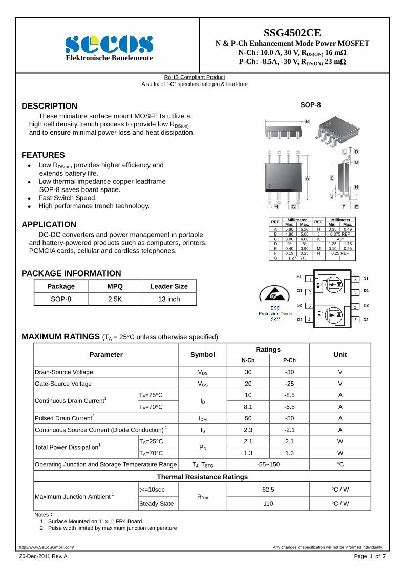
SSG4502CE N & P-Ch Enhancement Mode Power MOSFET
N-Ch: 10.0 A, 30 V, RDS(ON) 16 mΩΩΩΩ
P-Ch: -8.5A, -30 V, RDS(ON) 23 mΩΩΩΩ Elektronische Bauelemente
26-Dec-2011 Rev. A Page 1 of 7
http://www.SeCoSGmbH.com/ Any changes of specification will not be informed individually.
RoHS Compliant Product A suffix of “-C” specifies halogen & lead-free
DESCRIPTION These miniature surface mount MOSFETs utilize a
high cell density trench process to provide low RDS(on) and to ensure minimal power loss and heat dissipation.
FEATURES Low RDS(on) provides higher efficiency and
extends battery life. Low thermal impedance copper leadframe
SOP-8 saves board space. Fast Switch Speed. High performance trench technology.
APPLICATION DC-DC converters and power management in portable
and battery-powered products such as computers, printers, PCMCIA cards, cellular and cordless telephones.
PACKAGE INFORMATION
Package MPQ Leader Size
SOP-8 2.5K 13 inch
MAXIMUM RATINGS (TA = 25°C unless otherwise specified)
Parameter Symbol Ratings
Unit N-Ch P-Ch
Drain-Source Voltage VDS 30 -30 V
Gate-Source Voltage VGS 20 -25 V
Continuous Drain Current1 TA=25°C
ID 10 -8.5 A
TA=70°C 8.1 -6.8 A
Pulsed Drain Current2 IDM 50 -50 A
Continuous Source Current (Diode Conduction) 1 IS 2.3 -2.1 A
Total Power Dissipation1 TA=25°C
PD 2.1 2.1 W
TA=70°C 1.3 1.3 W
Operating Junction and Storage Temperature Range TJ, TSTG -55~150 °C
Thermal Resistance Ratings
Maximum Junction-Ambient 1 t<=10sec
RθJA 62.5 °C / W
Steady State 110 °C / W
Notes: 1. Surface Mounted on 1” x 1” FR4 Board. 2. Pulse width limited by maximum junction temperature
SOP-8
A
H
B
M
D
C
J K
F
L
E
N
G
REF. Millimeter REF. Millimeter Min. Max. Min. Max.
A 5.80 6.20 H 0.35 0.49 B 4.80 5.00 J 0.375 REF. C 3.80 4.00 K 45° D 0° 8° L 1.35 1.75 E 0.40 0.90 M 0.10 0.25 F 0.19 0.25 N 0.25 REF. G 1.27 TYP.
S1
G1
S2
D1
D1
D2
D2 G2
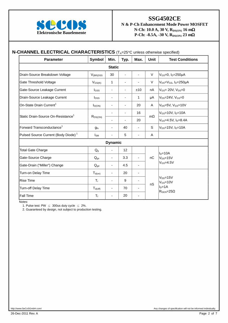
SSG4502CE N & P-Ch Enhancement Mode Power MOSFET
N-Ch: 10.0 A, 30 V, RDS(ON) 16 mΩΩΩΩ
P-Ch: -8.5A, -30 V, RDS(ON) 23 mΩΩΩΩ Elektronische Bauelemente
26-Dec-2011 Rev. A Page 2 of 7
http://www.SeCoSGmbH.com/ Any changes of specification will not be informed individually.
N-CHANNEL ELECTRICAL CHARACTERISTICS (TA=25°C unless otherwise specified)
Parameter Symbol Min. Typ. Max. Unit Test Conditions
Static
Drain-Source Breakdown Voltage V(BR)DSS 30 - - V VGS=0, ID=250µA
Gate Threshold Voltage VGS(th) 1 - - V VDS=VGS, ID=250µA
Gate-Source Leakage Current IGSS - - ±10 nA VGS= 20V, VDS=0
Drain-Source Leakage Current IDSS - - 1 µA VDS=24V, VGS=0
On-State Drain Current1 ID(ON) - - 20 A VDS=5V, VGS=10V
Static Drain-Source On-Resistance1 RDS(ON) - - 16
mΩ VGS=10V, ID=10A
- - 20 VGS=4.5V, ID=8.4A
Forward Transconductance1 gfs - 40 - S VDS=15V, ID=10A
Pulsed Source Current (Body Diode) 1 ISM - 5 - A
Dynamic
Total Gate Charge Qg - 12
nC ID=10A VDS=15V VGS=4.5V
Gate-Source Charge Qgs - 3.3 -
Gate-Drain (“Miller”) Change Qgd - 4.5 -
Turn-on Delay Time Td(on) - 20 -
nS
VDD=15V VGS=10V ID=1A RGEN=25Ω
Rise Time Tr - 9 -
Turn-off Delay Time Td(off) - 70 -
Fall Time Tf - 20 -
Notes: 1. Pulse test: PW ≦ 300us duty cycle ≦ 2%. 2. Guaranteed by design, not subject to production testing.
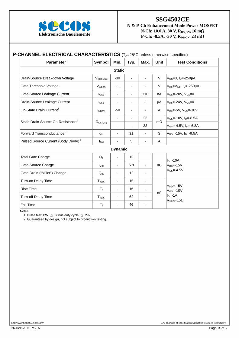
SSG4502CE N & P-Ch Enhancement Mode Power MOSFET
N-Ch: 10.0 A, 30 V, RDS(ON) 16 mΩΩΩΩ
P-Ch: -8.5A, -30 V, RDS(ON) 23 mΩΩΩΩ Elektronische Bauelemente
26-Dec-2011 Rev. A Page 3 of 7
http://www.SeCoSGmbH.com/ Any changes of specification will not be informed individually.
P-CHANNEL ELECTRICAL CHARACTERISTICS (TA=25°C unless otherwise specified)
Parameter Symbol Min. Typ. Max. Unit Test Conditions
Static
Drain-Source Breakdown Voltage V(BR)DSS -30 - - V VGS=0, ID=-250µA
Gate Threshold Voltage VGS(th) -1 - - V VDS=VGS, ID=-250µA
Gate-Source Leakage Current IGSS - - ±10 nA VGS=-20V, VDS=0
Drain-Source Leakage Current IDSS - - -1 µA VDS=-24V, VGS=0
On-State Drain Current1 ID(ON) -50 - - A VDS=-5V, VGS=-10V
Static Drain-Source On-Resistance1 RDS(ON) - - 23
mΩ VGS=-10V, ID=-8.5A
- - 33 VGS=-4.5V, ID=-6.8A
Forward Transconductance1 gfs - 31 - S VDS=-15V, ID=-9.5A
Pulsed Source Current (Body Diode) 1 ISM - 5 - A
Dynamic
Total Gate Charge Qg - 13
nC ID=-10A VDS=-15V VGS=-4.5V
Gate-Source Charge Qgs - 5.8 -
Gate-Drain (“Miller”) Change Qgd - 12 -
Turn-on Delay Time Td(on) - 15 -
nS
VDD=-15V VGS=-10V ID=-1A RGEN=15Ω
Rise Time Tr - 16 -
Turn-off Delay Time Td(off) - 62 -
Fall Time Tf - 46 -
Notes: 1. Pulse test: PW ≦ 300us duty cycle ≦ 2%. 2. Guaranteed by design, not subject to production testing.
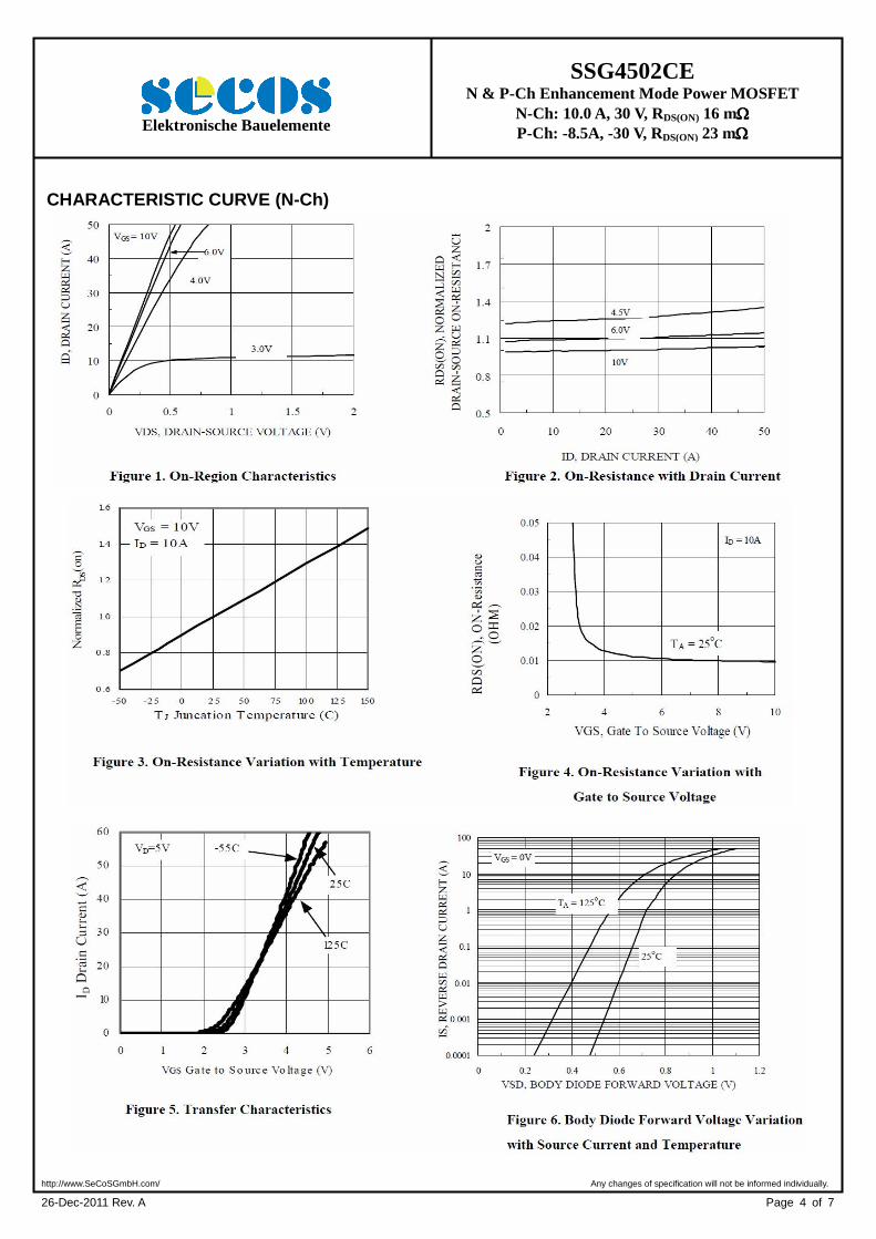
SSG4502CE N & P-Ch Enhancement Mode Power MOSFET
N-Ch: 10.0 A, 30 V, RDS(ON) 16 mΩΩΩΩ
P-Ch: -8.5A, -30 V, RDS(ON) 23 mΩΩΩΩ Elektronische Bauelemente
26-Dec-2011 Rev. A Page 4 of 7
http://www.SeCoSGmbH.com/ Any changes of specification will not be informed individually.
CHARACTERISTIC CURVE (N-Ch)
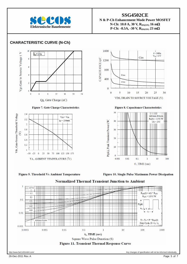
SSG4502CE N & P-Ch Enhancement Mode Power MOSFET
N-Ch: 10.0 A, 30 V, RDS(ON) 16 mΩΩΩΩ
P-Ch: -8.5A, -30 V, RDS(ON) 23 mΩΩΩΩ Elektronische Bauelemente
26-Dec-2011 Rev. A Page 5 of 7
http://www.SeCoSGmbH.com/ Any changes of specification will not be informed individually.
CHARACTERISTIC CURVE (N-Ch)
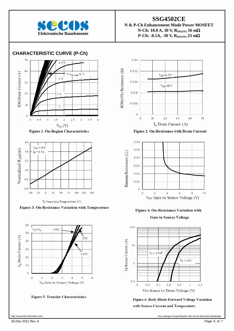
SSG4502CE N & P-Ch Enhancement Mode Power MOSFET
N-Ch: 10.0 A, 30 V, RDS(ON) 16 mΩΩΩΩ
P-Ch: -8.5A, -30 V, RDS(ON) 23 mΩΩΩΩ Elektronische Bauelemente
26-Dec-2011 Rev. A Page 6 of 7
http://www.SeCoSGmbH.com/ Any changes of specification will not be informed individually.
CHARACTERISTIC CURVE (P-Ch)
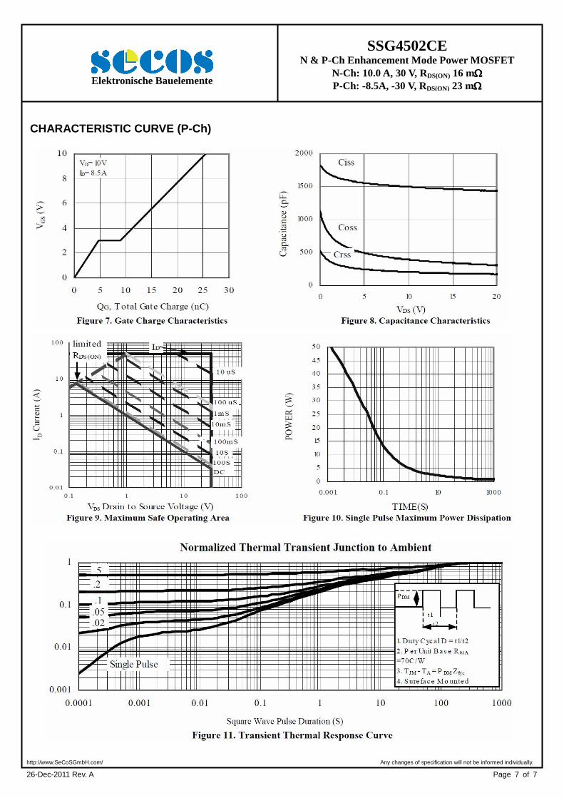
SSG4502CE N & P-Ch Enhancement Mode Power MOSFET
N-Ch: 10.0 A, 30 V, RDS(ON) 16 mΩΩΩΩ
P-Ch: -8.5A, -30 V, RDS(ON) 23 mΩΩΩΩ Elektronische Bauelemente
26-Dec-2011 Rev. A Page 7 of 7
http://www.SeCoSGmbH.com/ Any changes of specification will not be informed individually.
CHARACTERISTIC CURVE (P-Ch)