
SNx5LVDSxx High-Speed Differential Line Drivers · 7 v 300 k w 50 w vcc input vcc 5 w 7 v y or z...
49
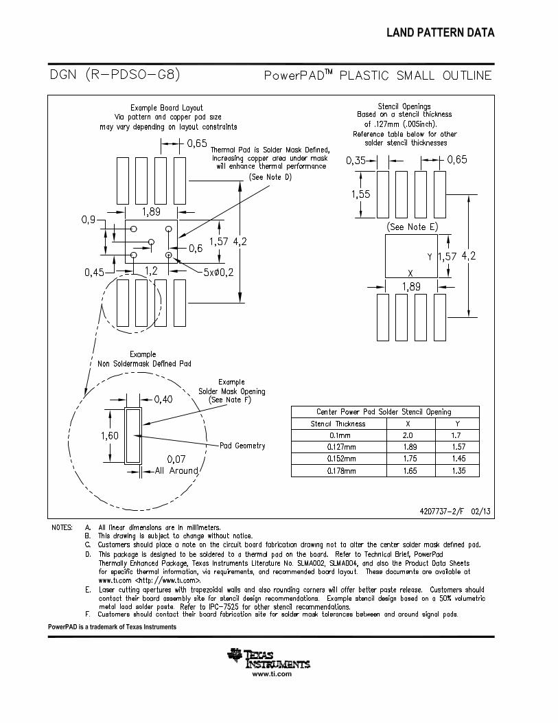
7 V 300 kΩ 50 Ω V CC Input V CC 5 Ω 7 V Y or Z Output EQUIVALENT OF EACH A INPUT EQUIVALENT OF G, G , 1,2EN OR 3,4EN INPUTS TYPICAL OF ALL OUTPUTS 7 V 50 Ω V CC Input 10 kΩ Product Folder Sample & Buy Technical Documents Tools & Software Support & Community SN55LVDS31, SN65LVDS31, SN65LVDS3487, SN65LVDS9638 SLLS261M – JULY 1997 – REVISED DECEMBER 2014 SNx5LVDSxx High-Speed Differential Line Drivers 1 Features 3 Description The SN55LVDS31, SN65LVDS31, SN65LVDS3487, 1• Meet or Exceed the Requirements of ANSI and SN65LVDS9638 devices are differential line TIA/EIA-644 Standard drivers that implement the electrical characteristics of • Low-Voltage Differential Signaling With Typical low-voltage differential signaling (LVDS). This Output Voltage of 350 mV and 100-Ω Load signaling technique lowers the output voltage levels of 5-V differential standard levels (such as TIA/EIA- • Typical Output Voltage Rise and Fall Times of 500 422B) to reduce the power, increase the switching ps (400 Mbps) speeds, and allow operation with a 3.3-V supply rail. • Typical Propagation Delay Times of 1.7 ns Any of the four current-mode drivers will deliver a • Operate From a Single 3.3-V Supply minimum differential output voltage magnitude of 247 • Power Dissipation 25 mW Typical Per Driver at mV into a 100-Ω load when enabled. 200 MHz Device Information (1) • Driver at High-Impedance When Disabled or With PART NUMBER PACKAGE BODY SIZE (NOM) V CC =0 LCCC (20) 8.89 mm × 8.89 mm • Bus-Terminal ESD Protection Exceeds 8 kV SN55LVDS31 CDIP (16) 19.56 mm × 6.92 mm • Low-Voltage TTL (LVTTL) Logic Input Levels CFP (16) 10.30 mm × 6.73 mm • Pin Compatible With AM26LS31, MC3487, and SOIC (16) 9.90 mm × 3.91 mm μA9638 SN65LVDS31 SOP (16) 10.30 mm × 5.30 mm • Cold Sparing for Space and High-Reliability TSSOP (16) 5.00 mm × 4.40 mm Applications Requiring Redundancy SOIC (16) 9.90 mm × 3.91 mm SN65LVDS3487 TSSOP (16) 5.00 mm × 4.40 mm 2 Applications SOIC (8) 4.90 mm × 3.91 mm • Wireless Infrastructure SN65LVDS9638 VSSOP (8) 3.00 mm × 3.00 mm • Telecom Infrastructure HVSSOP (8) 3.00 mm × 3.00 mm • Printers (1) For all available packages, see the orderable addendum at the end of the data sheet. Equivalent Input and Output Schematic Diagrams 1 An IMPORTANT NOTICE at the end of this data sheet addresses availability, warranty, changes, use in safety-critical applications, intellectual property matters and other important disclaimers. PRODUCTION DATA.
Transcript of SNx5LVDSxx High-Speed Differential Line Drivers · 7 v 300 k w 50 w vcc input vcc 5 w 7 v y or z...
7 V
300 kΩ
50 Ω
VCC
Input
VCC
5 Ω
7 V
Y or ZOutput
EQUIVALENT OF EACH A INPUT EQUIVALENT OF G, G, 1,2EN OR 3,4EN INPUTS TYPICAL OF ALL OUTPUTS
7 V
50 Ω
VCC
Input 10 kΩ
Product
Folder
Sample &Buy
Technical
Documents
Tools &
Software
Support &Community
SN55LVDS31, SN65LVDS31, SN65LVDS3487, SN65LVDS9638SLLS261M –JULY 1997–REVISED DECEMBER 2014
SNx5LVDSxx High-Speed Differential Line Drivers1 Features 3 Description
The SN55LVDS31, SN65LVDS31, SN65LVDS3487,1• Meet or Exceed the Requirements of ANSI
and SN65LVDS9638 devices are differential lineTIA/EIA-644 Standarddrivers that implement the electrical characteristics of
• Low-Voltage Differential Signaling With Typical low-voltage differential signaling (LVDS). ThisOutput Voltage of 350 mV and 100-Ω Load signaling technique lowers the output voltage levels
of 5-V differential standard levels (such as TIA/EIA-• Typical Output Voltage Rise and Fall Times of 500422B) to reduce the power, increase the switchingps (400 Mbps)speeds, and allow operation with a 3.3-V supply rail.• Typical Propagation Delay Times of 1.7 ns Any of the four current-mode drivers will deliver a
• Operate From a Single 3.3-V Supply minimum differential output voltage magnitude of 247• Power Dissipation 25 mW Typical Per Driver at mV into a 100-Ω load when enabled.
200 MHzDevice Information(1)
• Driver at High-Impedance When Disabled or WithPART NUMBER PACKAGE BODY SIZE (NOM)VCC = 0
LCCC (20) 8.89 mm × 8.89 mm• Bus-Terminal ESD Protection Exceeds 8 kVSN55LVDS31 CDIP (16) 19.56 mm × 6.92 mm• Low-Voltage TTL (LVTTL) Logic Input Levels
CFP (16) 10.30 mm × 6.73 mm• Pin Compatible With AM26LS31, MC3487, andSOIC (16) 9.90 mm × 3.91 mmμA9638
SN65LVDS31 SOP (16) 10.30 mm × 5.30 mm• Cold Sparing for Space and High-ReliabilityTSSOP (16) 5.00 mm × 4.40 mmApplications Requiring RedundancySOIC (16) 9.90 mm × 3.91 mm
SN65LVDS3487TSSOP (16) 5.00 mm × 4.40 mm2 ApplicationsSOIC (8) 4.90 mm × 3.91 mm• Wireless Infrastructure
SN65LVDS9638 VSSOP (8) 3.00 mm × 3.00 mm• Telecom InfrastructureHVSSOP (8) 3.00 mm × 3.00 mm
• Printers(1) For all available packages, see the orderable addendum at
the end of the data sheet.
Equivalent Input and Output Schematic Diagrams
1
An IMPORTANT NOTICE at the end of this data sheet addresses availability, warranty, changes, use in safety-critical applications,intellectual property matters and other important disclaimers. PRODUCTION DATA.
SN55LVDS31, SN65LVDS31, SN65LVDS3487, SN65LVDS9638SLLS261M –JULY 1997–REVISED DECEMBER 2014 www.ti.com
Table of Contents9.2 Functional Block Diagram ....................................... 141 Features .................................................................. 19.3 Feature Description................................................. 142 Applications ........................................................... 19.4 Device Functional Modes........................................ 163 Description ............................................................. 1
10 Application and Implementation........................ 174 Revision History..................................................... 210.1 Application Information.......................................... 175 Description (Continued) ........................................ 310.2 Typical Application ................................................ 176 Pin Configuration and Functions ......................... 4
11 Power Supply Recommendations ..................... 237 Specifications......................................................... 612 Layout................................................................... 237.1 Absolute Maximum Ratings ..................................... 6
12.1 Layout Guidelines ................................................. 237.2 ESD Ratings.............................................................. 612.2 Layout Example .................................................... 257.3 Recommended Operating Conditions....................... 7
13 Device and Documentation Support ................. 277.4 Thermal Information .................................................. 713.1 Device Support...................................................... 277.5 Electrical Characteristics: SN55LVDS31 .................. 813.2 Documentation Support ........................................ 277.6 Electrical Characteristics: SN65LVDSxxxx ............... 913.3 Related Links ........................................................ 277.7 Switching Characteristics: SN55LVDS31 ................. 913.4 Trademarks ........................................................... 277.8 Switching Characteristics: SN65LVDSxxxx ............ 1013.5 Electrostatic Discharge Caution............................ 277.9 Typical Characteristics ............................................ 1113.6 Glossary ................................................................ 278 Parameter Measurement Information ................ 12
14 Mechanical, Packaging, and Orderable9 Detailed Description ............................................ 14 Information ........................................................... 289.1 Overview ................................................................. 14
4 Revision History
Changes from Revision L (July 2007) to Revision M Page
• Added Pin Configuration and Functions section, ESD Ratings table, Feature Description section, Device FunctionalModes, Application and Implementation section, Power Supply Recommendations section, Layout section, Deviceand Documentation Support section, and Mechanical, Packaging, and Orderable Information section .............................. 1
Changes from Revision K (March 2004) to Revision L Page
• Added Cold Sparing Feature .................................................................................................................................................. 1• Added Cold Sparing information........................................................................................................................................... 14
2 Submit Documentation Feedback Copyright © 1997–2014, Texas Instruments Incorporated
Product Folder Links: SN55LVDS31 SN65LVDS31 SN65LVDS3487 SN65LVDS9638
SN55LVDS31, SN65LVDS31, SN65LVDS3487, SN65LVDS9638www.ti.com SLLS261M –JULY 1997–REVISED DECEMBER 2014
5 Description (Continued)The intended application of these devices and signaling technique is both point-to-point and multidrop (one driverand multiple receivers) data transmission over controlled impedance media of approximately 100 Ω. Thetransmission media may be printed-circuit board traces, backplanes, or cables. The ultimate rate and distance ofdata transfer is dependent upon the attenuation characteristics of the media and the noise coupling to theenvironment.
The SN65LVDS31, SN65LVDS3487, and SN65LVDS9638 devices are characterized for operation from –40°C to85°C. The SN55LVDS31 device is characterized for operation from –55°C to 125°C.
Copyright © 1997–2014, Texas Instruments Incorporated Submit Documentation Feedback 3
Product Folder Links: SN55LVDS31 SN65LVDS31 SN65LVDS3487 SN65LVDS9638
1
2
3
4
5
6
7
8
16
15
14
13
12
11
10
9
1A1Y1ZG
2Z2Y2A
GND
VCC
4A4Y4ZG3Z3Y3A
SN55LVDS31 . . . J OR WSN65LVDS31 . . . D OR PW
(Marked as LVDS31 or 65LVDS31)(TOP VIEW)
1
2
3
4
5
6
7
8
16
15
14
13
12
11
10
9
1A1Y1Z
1,2EN2Z2Y2A
GND
VCC
4A4Y4Z3,4EN3Z3Y3A
SN65LVDS3487D(Marked as LVDS3487 or 65LVDS3487)
(TOP VIEW)
1
2
3
4
8
7
6
5
VCC
1A2A
GND
1Y1Z2Y2Z
SN65LVDS9638D (Marked as DK638 or LVDS38)SN65LVDS9638DGN (Marked as L38)SN65LVDS9638DGK (Marked as AXG)
(TOP VIEW)
192013 2
17
18
16
15
14
1312119 10
5
4
6
7
8
4Y
4Z
NC
G
3Z
1Z
G
NC
2Z
2Y
1Y 1A NC
V 4A
GN
D
NC 3A 3Y2A
SN55LVDS31FK(TOP VIEW)
CC
SN55LVDS31, SN65LVDS31, SN65LVDS3487, SN65LVDS9638SLLS261M –JULY 1997–REVISED DECEMBER 2014 www.ti.com
6 Pin Configuration and Functions
4 Submit Documentation Feedback Copyright © 1997–2014, Texas Instruments Incorporated
Product Folder Links: SN55LVDS31 SN65LVDS31 SN65LVDS3487 SN65LVDS9638
SN55LVDS31, SN65LVDS31, SN65LVDS3487, SN65LVDS9638www.ti.com SLLS261M –JULY 1997–REVISED DECEMBER 2014
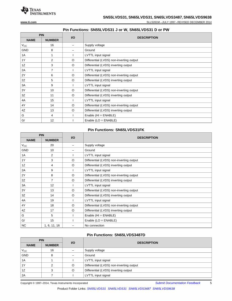
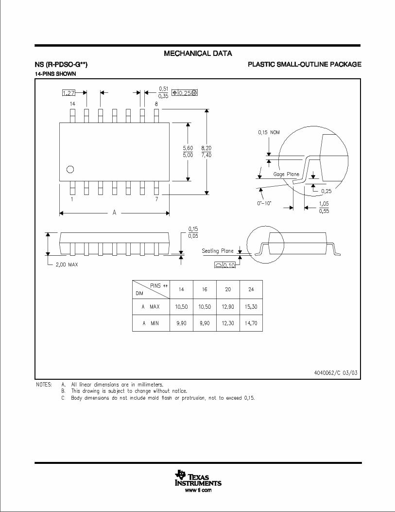
Pin Functions: SN55LVDS31 J or W, SN65LVDS31 D or PWPIN
I/O DESCRIPTIONNAME NUMBER
VCC 16 – Supply voltageGND 8 – Ground1A 1 I LVTTL input signal1Y 2 O Differential (LVDS) non-inverting output1Z 3 O Differential (LVDS) inverting output2A 7 I LVTTL input signal2Y 6 O Differential (LVDS) non-inverting output2Z 5 O Differential (LVDS) inverting output3A 9 I LVTTL input signal3Y 10 O Differential (LVDS) non-inverting output3Z 11 O Differential (LVDS) inverting output4A 15 I LVTTL input signal4Y 14 O Differential (LVDS) non-inverting output4Z 13 O Differential (LVDS) inverting outputG 4 I Enable (HI = ENABLE)G/ 12 I Enable (LO = ENABLE)
Pin Functions: SN65LVDS31FKPIN
I/O DESCRIPTIONNAME NUMBER
VCC 20 – Supply voltageGND 10 – Ground1A 2 I LVTTL input signal1Y 3 O Differential (LVDS) non-inverting output1Z 4 O Differential (LVDS) inverting output2A 9 I LVTTL input signal2Y 8 O Differential (LVDS) non-inverting output2Z 7 O Differential (LVDS) inverting output3A 12 I LVTTL input signal3Y 13 O Differential (LVDS) non-inverting output3Z 14 O Differential (LVDS) inverting output4A 19 I LVTTL input signal4Y 18 O Differential (LVDS) non-inverting output4Z 17 O Differential (LVDS) inverting outputG 5 I Enable (HI = ENABLE)G/ 15 I Enable (LO = ENABLE)NC 1, 6, 11, 16 – No connection
Pin Functions: SN65LVDS3487DPIN
I/O DESCRIPTIONNAME NUMBER
VCC 16 – Supply voltageGND 8 – Ground1A 1 I LVTTL input signal1Y 2 O Differential (LVDS) non-inverting output1Z 3 O Differential (LVDS) inverting output2A 7 I LVTTL input signal
Copyright © 1997–2014, Texas Instruments Incorporated Submit Documentation Feedback 5
Product Folder Links: SN55LVDS31 SN65LVDS31 SN65LVDS3487 SN65LVDS9638
SN55LVDS31, SN65LVDS31, SN65LVDS3487, SN65LVDS9638SLLS261M –JULY 1997–REVISED DECEMBER 2014 www.ti.com
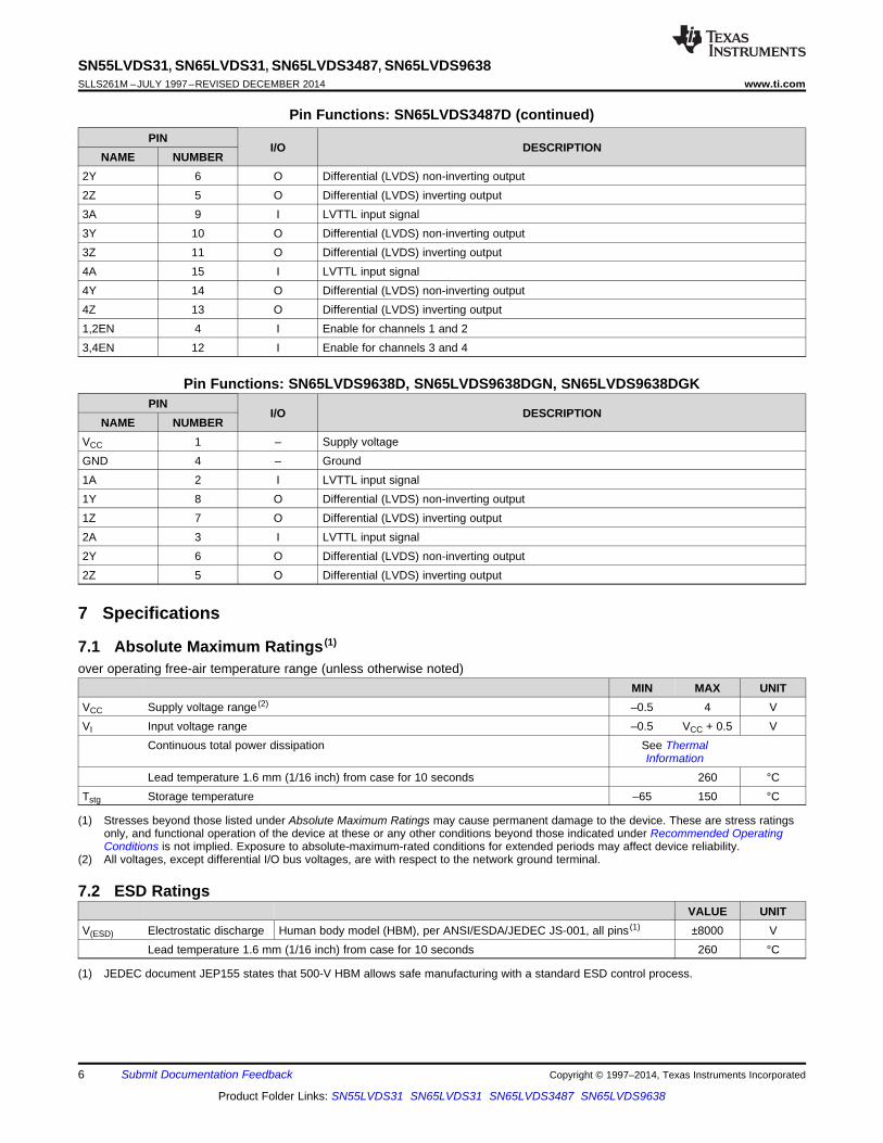
Pin Functions: SN65LVDS3487D (continued)PIN
I/O DESCRIPTIONNAME NUMBER
2Y 6 O Differential (LVDS) non-inverting output2Z 5 O Differential (LVDS) inverting output3A 9 I LVTTL input signal3Y 10 O Differential (LVDS) non-inverting output3Z 11 O Differential (LVDS) inverting output4A 15 I LVTTL input signal4Y 14 O Differential (LVDS) non-inverting output4Z 13 O Differential (LVDS) inverting output1,2EN 4 I Enable for channels 1 and 23,4EN 12 I Enable for channels 3 and 4
Pin Functions: SN65LVDS9638D, SN65LVDS9638DGN, SN65LVDS9638DGKPIN
I/O DESCRIPTIONNAME NUMBER
VCC 1 – Supply voltageGND 4 – Ground1A 2 I LVTTL input signal1Y 8 O Differential (LVDS) non-inverting output1Z 7 O Differential (LVDS) inverting output2A 3 I LVTTL input signal2Y 6 O Differential (LVDS) non-inverting output2Z 5 O Differential (LVDS) inverting output
7 Specifications
7.1 Absolute Maximum Ratings (1)
over operating free-air temperature range (unless otherwise noted)MIN MAX UNIT
VCC Supply voltage range (2) –0.5 4 VVI Input voltage range –0.5 VCC + 0.5 V
Continuous total power dissipation See ThermalInformation
Lead temperature 1.6 mm (1/16 inch) from case for 10 seconds 260 °CTstg Storage temperature –65 150 °C
(1) Stresses beyond those listed under Absolute Maximum Ratings may cause permanent damage to the device. These are stress ratingsonly, and functional operation of the device at these or any other conditions beyond those indicated under Recommended OperatingConditions is not implied. Exposure to absolute-maximum-rated conditions for extended periods may affect device reliability.
(2) All voltages, except differential I/O bus voltages, are with respect to the network ground terminal.
7.2 ESD RatingsVALUE UNIT
V(ESD) Electrostatic discharge Human body model (HBM), per ANSI/ESDA/JEDEC JS-001, all pins (1) ±8000 VLead temperature 1.6 mm (1/16 inch) from case for 10 seconds 260 °C
(1) JEDEC document JEP155 states that 500-V HBM allows safe manufacturing with a standard ESD control process.
6 Submit Documentation Feedback Copyright © 1997–2014, Texas Instruments Incorporated
Product Folder Links: SN55LVDS31 SN65LVDS31 SN65LVDS3487 SN65LVDS9638
SN55LVDS31, SN65LVDS31, SN65LVDS3487, SN65LVDS9638www.ti.com SLLS261M –JULY 1997–REVISED DECEMBER 2014
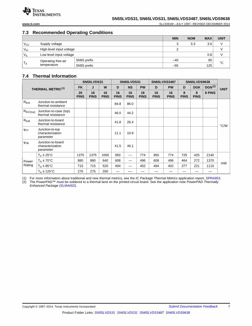
7.3 Recommended Operating ConditionsMIN NOM MAX UNIT
VCC Supply voltage 3 3.3 3.6 VVIH High-level input voltage 2 VVIL Low-level input voltage 0.8 V
SN65 prefix –40 85Operating free-airTA °Ctemperature SN55 prefix –55 125
7.4 Thermal InformationSN55LVDS31 SN65LVDS31 SN65LVDS3487 SN65LVDS9638
FK J W D NS PW D PW D DGK DGN (2)THERMAL METRIC (1) UNIT
20 16 16 16 16 16 16 16 8 8 8 PINSPINS PINS PINS PINS PINS PINS PINS PINS PINS PINS
RθJA Junction-to-ambient 84.8 86.0thermal resistanceRθJC(top) Junction-to-case (top) 46.0 44.2thermal resistanceRθJB Junction-to-board 41.8 26.4thermal resistance °C/WψJT Junction-to-top
characterization 11.1 10.9parameter
ψJB Junction-to-boardcharacterization 41.5 46.1parameterTA ≤ 25°C 1375 1375 1000 950 — 774 950 774 725 425 2140TA ≤ 70°C 880 880 640 608 — 496 608 496 464 272 1370Power mWRating TA ≤ 85°C 715 715 520 494 — 402 494 402 377 221 1110TA ≤ 125°C 275 275 200 — —- — — — — — —
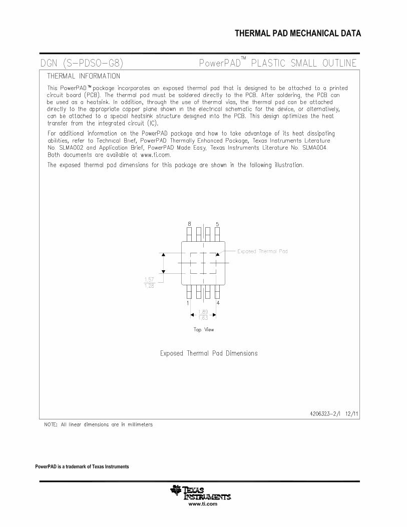
(1) For more information about traditional and new thermal metrics, see the IC Package Thermal Metrics application report, SPRA953.(2) The PowerPAD™ must be soldered to a thermal land on the printed-circuit board. See the application note PowerPAD Thermally
Enhanced Package (SLMA002).
Copyright © 1997–2014, Texas Instruments Incorporated Submit Documentation Feedback 7
Product Folder Links: SN55LVDS31 SN65LVDS31 SN65LVDS3487 SN65LVDS9638
SN55LVDS31, SN65LVDS31, SN65LVDS3487, SN65LVDS9638SLLS261M –JULY 1997–REVISED DECEMBER 2014 www.ti.com
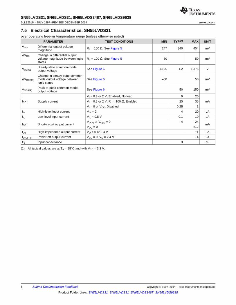
7.5 Electrical Characteristics: SN55LVDS31over operating free-air temperature range (unless otherwise noted)
PARAMETER TEST CONDITIONS MIN TYP (1) MAX UNITVOD Differential output voltage RL = 100 Ω, See Figure 5 247 340 454 mVmagnitudeΔVOD Change in differential output
voltage magnitude between logic RL = 100 Ω, See Figure 5 –50 50 mVstatesSteady-state common-modeVOC(SS) See Figure 6 1.125 1.2 1.375 Voutput voltageChange in steady-state common-
ΔVOC(SS) mode output voltage between See Figure 6 –50 50 mVlogic statesPeak-to-peak common-modeVOC(PP) See Figure 6 50 150 mVoutput voltage
VI = 0.8 or 2 V, Enabled, No load 9 20ICC Supply current VI = 0.8 or 2 V, RL = 100 Ω, Enabled 25 35 mA
VI = 0 or VCC, Disabled 0.25 1IIH High-level input current VIH = 2 4 20 μAIIL Low-level input current VIL = 0.8 V 0.1 10 μA
VO(Y) or VO(Z) = 0 –4 –24IOS Short-circuit output current mA
VOD = 0 ±12IOZ High-impedance output current VO = 0 or 2.4 V ±1 μAIO(OFF) Power-off output current VCC = 0, VO = 2.4 V ±4 μACi Input capacitance 3 pF
(1) All typical values are at TA = 25°C and with VCC = 3.3 V.
8 Submit Documentation Feedback Copyright © 1997–2014, Texas Instruments Incorporated
Product Folder Links: SN55LVDS31 SN65LVDS31 SN65LVDS3487 SN65LVDS9638
SN55LVDS31, SN65LVDS31, SN65LVDS3487, SN65LVDS9638www.ti.com SLLS261M –JULY 1997–REVISED DECEMBER 2014
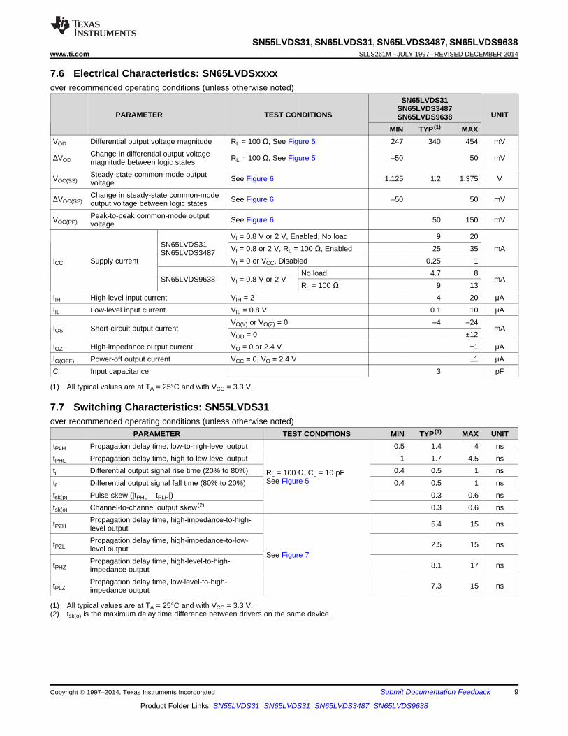
7.6 Electrical Characteristics: SN65LVDSxxxxover recommended operating conditions (unless otherwise noted)
SN65LVDS31SN65LVDS3487
PARAMETER TEST CONDITIONS UNITSN65LVDS9638MIN TYP (1) MAX
VOD Differential output voltage magnitude RL = 100 Ω, See Figure 5 247 340 454 mVChange in differential output voltageΔVOD RL = 100 Ω, See Figure 5 –50 50 mVmagnitude between logic statesSteady-state common-mode outputVOC(SS) See Figure 6 1.125 1.2 1.375 VvoltageChange in steady-state common-modeΔVOC(SS) See Figure 6 –50 50 mVoutput voltage between logic statesPeak-to-peak common-mode outputVOC(PP) See Figure 6 50 150 mVvoltage
VI = 0.8 V or 2 V, Enabled, No load 9 20SN65LVDS31 VI = 0.8 or 2 V, RL = 100 Ω, Enabled 25 35 mASN65LVDS3487
ICC Supply current VI = 0 or VCC, Disabled 0.25 1No load 4.7 8
SN65LVDS9638 VI = 0.8 V or 2 V mARL = 100 Ω 9 13
IIH High-level input current VIH = 2 4 20 μAIIL Low-level input current VIL = 0.8 V 0.1 10 μA
VO(Y) or VO(Z) = 0 –4 –24IOS Short-circuit output current mA
VOD = 0 ±12IOZ High-impedance output current VO = 0 or 2.4 V ±1 μAIO(OFF) Power-off output current VCC = 0, VO = 2.4 V ±1 μACi Input capacitance 3 pF
(1) All typical values are at TA = 25°C and with VCC = 3.3 V.
7.7 Switching Characteristics: SN55LVDS31over recommended operating conditions (unless otherwise noted)
PARAMETER TEST CONDITIONS MIN TYP (1) MAX UNITtPLH Propagation delay time, low-to-high-level output 0.5 1.4 4 nstPHL Propagation delay time, high-to-low-level output 1 1.7 4.5 nstr Differential output signal rise time (20% to 80%) 0.4 0.5 1 nsRL = 100 Ω, CL = 10 pF
See Figure 5tf Differential output signal fall time (80% to 20%) 0.4 0.5 1 nstsk(p) Pulse skew (|tPHL – tPLH|) 0.3 0.6 nstsk(o) Channel-to-channel output skew (2) 0.3 0.6 ns
Propagation delay time, high-impedance-to-high-tPZH 5.4 15 nslevel outputPropagation delay time, high-impedance-to-low-tPZL 2.5 15 nslevel output
See Figure 7Propagation delay time, high-level-to-high-tPHZ 8.1 17 nsimpedance outputPropagation delay time, low-level-to-high-tPLZ 7.3 15 nsimpedance output
(1) All typical values are at TA = 25°C and with VCC = 3.3 V.(2) tsk(o) is the maximum delay time difference between drivers on the same device.
Copyright © 1997–2014, Texas Instruments Incorporated Submit Documentation Feedback 9
Product Folder Links: SN55LVDS31 SN65LVDS31 SN65LVDS3487 SN65LVDS9638
SN55LVDS31, SN65LVDS31, SN65LVDS3487, SN65LVDS9638SLLS261M –JULY 1997–REVISED DECEMBER 2014 www.ti.com
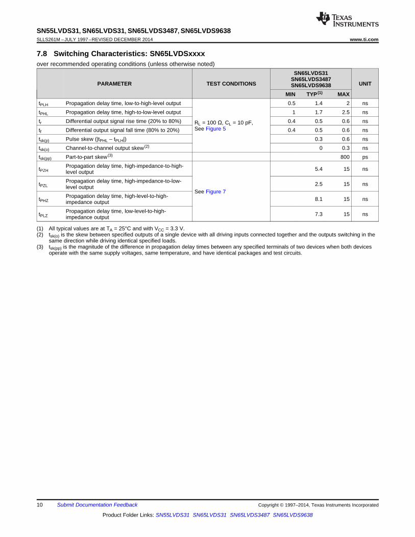
7.8 Switching Characteristics: SN65LVDSxxxxover recommended operating conditions (unless otherwise noted)
SN65LVDS31SN65LVDS3487
PARAMETER TEST CONDITIONS UNITSN65LVDS9638MIN TYP (1) MAX
tPLH Propagation delay time, low-to-high-level output 0.5 1.4 2 nstPHL Propagation delay time, high-to-low-level output 1 1.7 2.5 nstr Differential output signal rise time (20% to 80%) 0.4 0.5 0.6 nsRL = 100 Ω, CL = 10 pF,
See Figure 5tf Differential output signal fall time (80% to 20%) 0.4 0.5 0.6 nstsk(p) Pulse skew (|tPHL – tPLH|) 0.3 0.6 nstsk(o) Channel-to-channel output skew (2) 0 0.3 nstsk(pp) Part-to-part skew (3) 800 ps
Propagation delay time, high-impedance-to-high-tPZH 5.4 15 nslevel outputPropagation delay time, high-impedance-to-low-tPZL 2.5 15 nslevel output
See Figure 7Propagation delay time, high-level-to-high-tPHZ 8.1 15 nsimpedance outputPropagation delay time, low-level-to-high-tPLZ 7.3 15 nsimpedance output
(1) All typical values are at TA = 25°C and with VCC = 3.3 V.(2) tsk(o) is the skew between specified outputs of a single device with all driving inputs connected together and the outputs switching in the
same direction while driving identical specified loads.(3) tsk(pp) is the magnitude of the difference in propagation delay times between any specified terminals of two devices when both devices
operate with the same supply voltages, same temperature, and have identical packages and test circuits.
10 Submit Documentation Feedback Copyright © 1997–2014, Texas Instruments Incorporated
Product Folder Links: SN55LVDS31 SN65LVDS31 SN65LVDS3487 SN65LVDS9638
1.5
1.4
1.2
1
1.7
1.9
−40 −20 0 20 40
TA − Free-Air T emperature − °C
VCC = 3 V1.8
1.6
1.3
1.1
60 80 100
VCC = 3.3 V
VCC = 3.6 V
t PH
L−
Hig
h-to
-Low
Pro
paga
tion
Del
ay T
ime
− ns
1.5
1.4
1.2
1
1.7
1.9
−40 −20 0 20 40TA − Free-Air T emperature − °C
VCC = 3 V
VCC = 3.6 V
1.8
1.6
1.3
1.1
60 80 100
VCC = 3.3 V
− Lo
w-to
-Hig
h P
ropa
gatio
n D
elay
Tim
e −
nst P
LH
SN55LVDS31, SN65LVDS31, SN65LVDS3487, SN65LVDS9638www.ti.com SLLS261M –JULY 1997–REVISED DECEMBER 2014
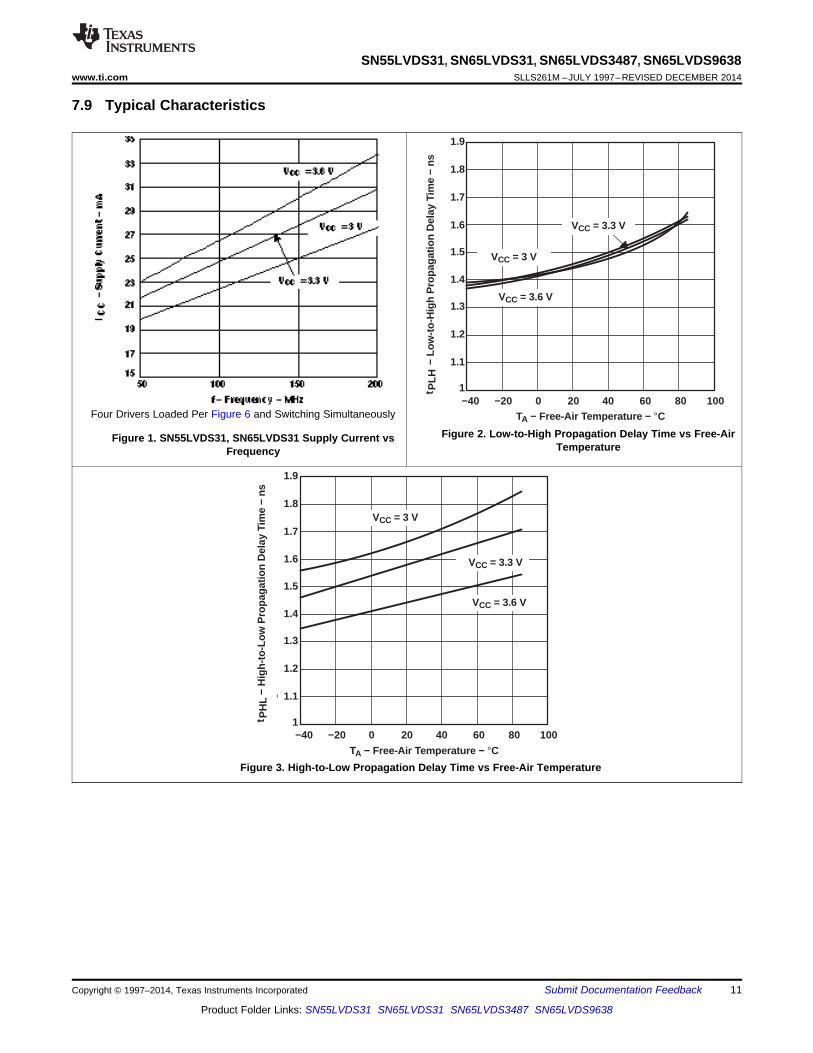
7.9 Typical Characteristics
Four Drivers Loaded Per Figure 6 and Switching Simultaneously
Figure 2. Low-to-High Propagation Delay Time vs Free-AirFigure 1. SN55LVDS31, SN65LVDS31 Supply Current vsTemperatureFrequency
Figure 3. High-to-Low Propagation Delay Time vs Free-Air Temperature
Copyright © 1997–2014, Texas Instruments Incorporated Submit Documentation Feedback 11
Product Folder Links: SN55LVDS31 SN65LVDS31 SN65LVDS3487 SN65LVDS9638
Y
Z
Input(see Note A)
CL = 10 pF(2 Places)(see Note B)
49.9 Ω ± 1% (2 Places)
VOC
AA
VOC
VOC(PP)
(see Note C) VOC(SS)
0
3 V
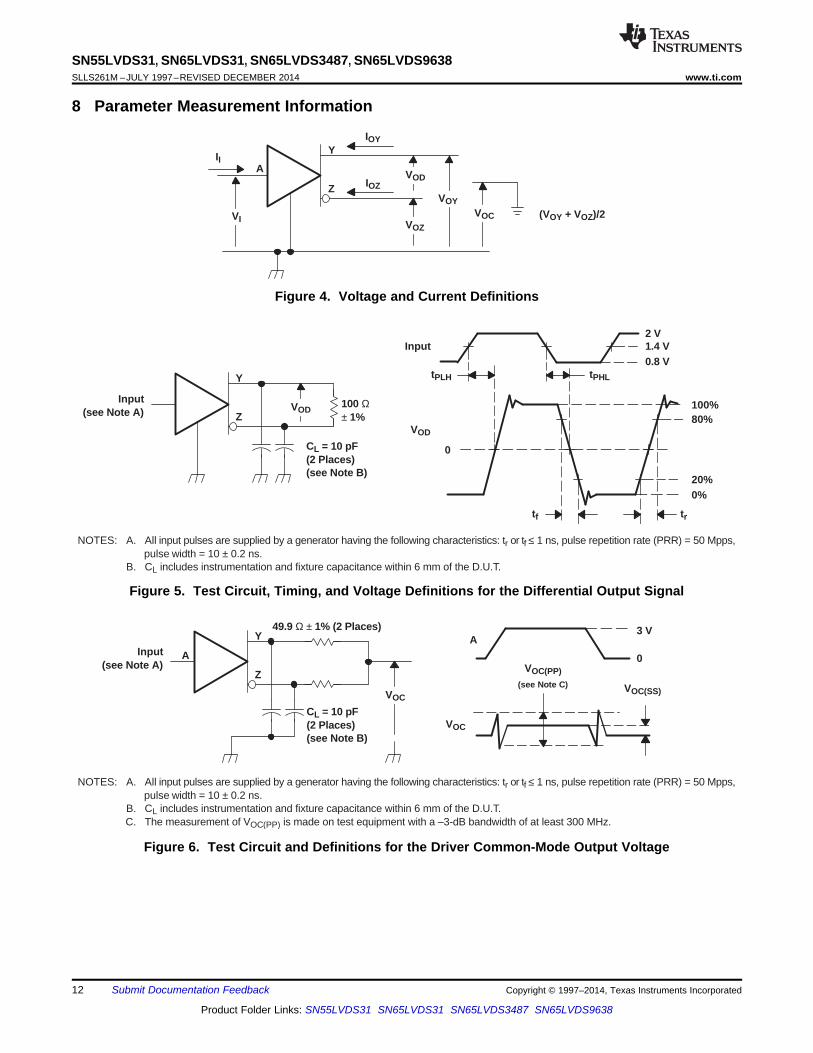
NOTES: A. All input pulses are supplied by a generator having the following characteristics: tr or tf ≤ 1 ns, pulse repetition rate (PRR) = 50 Mpps,pulse width = 10 ± 0.2 ns.
B. CL includes instrumentation and fixture capacitance within 6 mm of the D.U.T.C. The measurement of VOC(PP) is made on test equipment with a –3-dB bandwidth of at least 300 MHz.
Y
ZVOD
Input(see Note A)
CL = 10 pF(2 Places)(see Note B)
100 Ω ± 1%
2 V1.4 V0.8 V
tPLH tPHL
100%80%
20%0%
Input
VOD
0
tf tr
NOTES: A. All input pulses are supplied by a generator having the following characteristics: tr or tf ≤ 1 ns, pulse repetition rate (PRR) = 50 Mpps,pulse width = 10 ± 0.2 ns.
B. CL includes instrumentation and fixture capacitance within 6 mm of the D.U.T.
VI
A
(VOY + VOZ)/2
IOZ
IOYY
ZVOD
VOYVOC
II
VOZ
SN55LVDS31, SN65LVDS31, SN65LVDS3487, SN65LVDS9638SLLS261M –JULY 1997–REVISED DECEMBER 2014 www.ti.com
8 Parameter Measurement Information
Figure 4. Voltage and Current Definitions
Figure 5. Test Circuit, Timing, and Voltage Definitions for the Differential Output Signal
Figure 6. Test Circuit and Definitions for the Driver Common-Mode Output Voltage
12 Submit Documentation Feedback Copyright © 1997–2014, Texas Instruments Incorporated
Product Folder Links: SN55LVDS31 SN65LVDS31 SN65LVDS3487 SN65LVDS9638
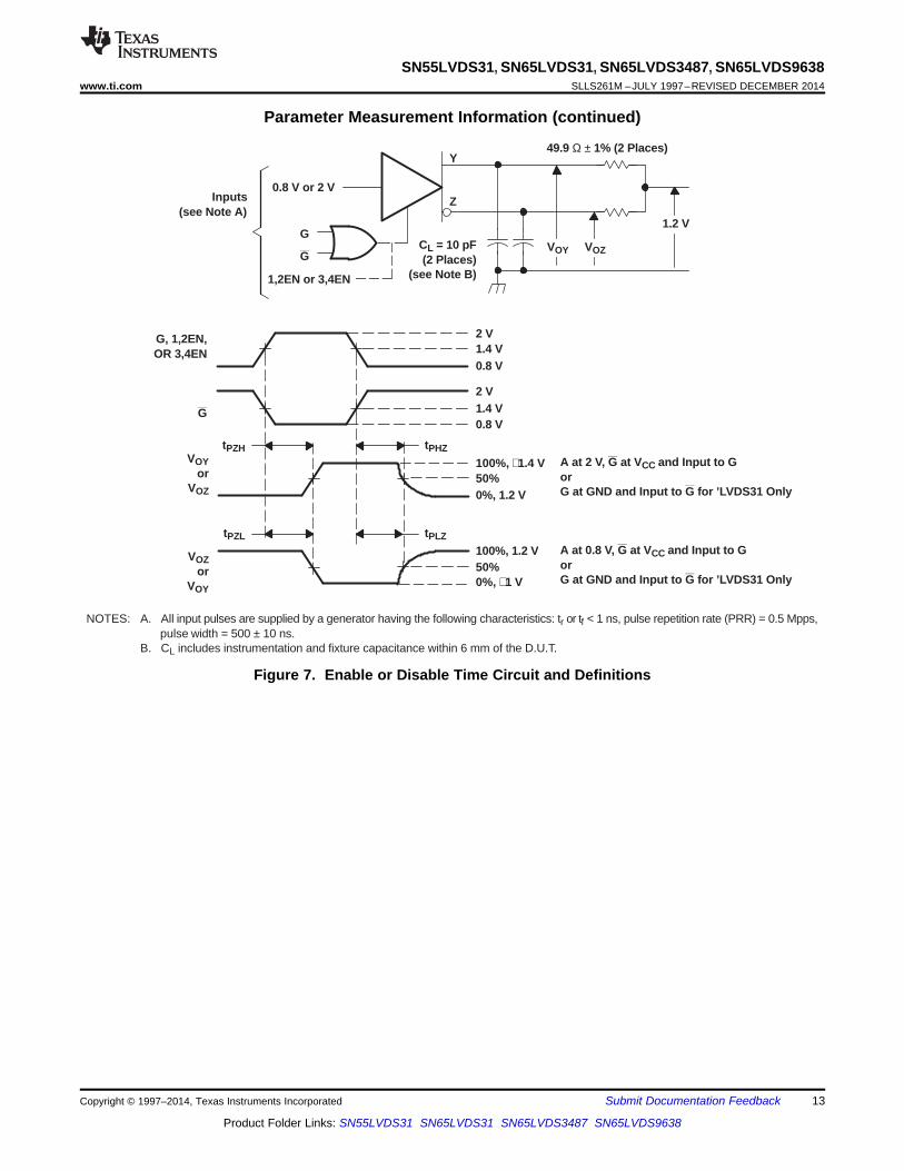
Y
ZInputs(see Note A)
CL = 10 pF(2 Places)
(see Note B)
49.9 Ω ± 1% (2 Places)
G
G
1.2 V
tPZH tPHZ
tPZL tPLZ
2 V1.4 V0.8 V
100%, ≅ 1.4 V
1.4 V2 V
0.8 V
50%0%, 1.2 V
0%, ≅ 1 V
100%, 1.2 V50%
G, 1,2EN,OR 3,4EN
G
VOYor
VOZ
VOZor
VOY
A at 2 V, G at VCC and Input to GorG at GND and Input to G for ’LVDS31 Only
A at 0.8 V, G at VCC and Input to GorG at GND and Input to G for ’LVDS31 Only
VOY VOZ
0.8 V or 2 V
1,2EN or 3,4EN
NOTES: A. All input pulses are supplied by a generator having the following characteristics: tr or tf < 1 ns, pulse repetition rate (PRR) = 0.5 Mpps,pulse width = 500 ± 10 ns.
B. CL includes instrumentation and fixture capacitance within 6 mm of the D.U.T.
SN55LVDS31, SN65LVDS31, SN65LVDS3487, SN65LVDS9638www.ti.com SLLS261M –JULY 1997–REVISED DECEMBER 2014
Parameter Measurement Information (continued)
Figure 7. Enable or Disable Time Circuit and Definitions
Copyright © 1997–2014, Texas Instruments Incorporated Submit Documentation Feedback 13
Product Folder Links: SN55LVDS31 SN65LVDS31 SN65LVDS3487 SN65LVDS9638
SN65LVDS9638 logic diagram (positive logic)
2Z
2Y
1Z
1Y
5
6
7
8
2A
1A2
3
’LVDS31 logic diagram (positive logic)
4Z
4Y
3Z
3Y
2Z
2Y
1Z
1Y
13
14
11
10
5
6
3
2
4A
3A
2A
1A
G
G
15
9
7
1
12
4
SN65LVDS3487 logic diagram(positive logic)
4Z
4Y
3Z
3Y
2Z
2Y
1Z
1Y
13
14
11
10
5
6
3
2
4A
3A
2A
1A
15
9
1
4
7
123,4EN
1,2EN
SN55LVDS31, SN65LVDS31, SN65LVDS3487, SN65LVDS9638SLLS261M –JULY 1997–REVISED DECEMBER 2014 www.ti.com
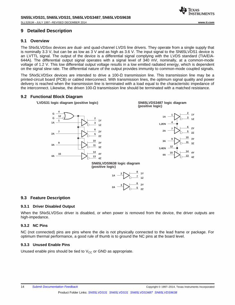
9 Detailed Description
9.1 OverviewThe SNx5LVDSxx devices are dual- and quad-channel LVDS line drivers. They operate from a single supply thatis nominally 3.3 V, but can be as low as 3 V and as high as 3.6 V. The input signal to the SN65LVDS1 device isan LVTTL signal. The output of the device is a differential signal complying with the LVDS standard (TIA/EIA-644A). The differential output signal operates with a signal level of 340 mV, nominally, at a common-modevoltage of 1.2 V. This low differential output voltage results in a low emitted radiated energy, which is dependenton the signal slew rate. The differential nature of the output provides immunity to common-mode coupled signals.
The SNx5LVDSxx devices are intended to drive a 100-Ω transmission line. This transmission line may be aprinted-circuit board (PCB) or cabled interconnect. With transmission lines, the optimum signal quality and powerdelivery is reached when the transmission line is terminated with a load equal to the characteristic impedance ofthe interconnect. Likewise, the driven 100-Ω transmission line should be terminated with a matched resistance.
9.2 Functional Block Diagram
9.3 Feature Description
9.3.1 Driver Disabled OutputWhen the SNx5LVDSxx driver is disabled, or when power is removed from the device, the driver outputs arehigh-impedance.
9.3.2 NC PinsNC (not connected) pins are pins where the die is not physically connected to the lead frame or package. Foroptimum thermal performance, a good rule of thumb is to ground the NC pins at the board level.
9.3.3 Unused Enable PinsUnused enable pins should be tied to VCC or GND as appropriate.
14 Submit Documentation Feedback Copyright © 1997–2014, Texas Instruments Incorporated
Product Folder Links: SN55LVDS31 SN65LVDS31 SN65LVDS3487 SN65LVDS9638
7 V
300 kΩ
50 Ω
VCC
Input
VCC
5 Ω
7 V
Y or ZOutput
EQUIVALENT OF EACH A INPUT EQUIVALENT OF G, G, 1,2EN OR 3,4EN INPUTS TYPICAL OF ALL OUTPUTS
7 V
50 Ω
VCC
Input 10 kΩ
SN55LVDS31, SN65LVDS31, SN65LVDS3487, SN65LVDS9638www.ti.com SLLS261M –JULY 1997–REVISED DECEMBER 2014
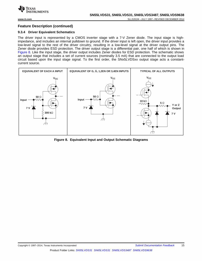
Feature Description (continued)9.3.4 Driver Equivalent SchematicsThe driver input is represented by a CMOS inverter stage with a 7-V Zener diode. The input stage is high-impedance, and includes an internal pulldown to ground. If the driver input is left open, the driver input provides alow-level signal to the rest of the driver circuitry, resulting in a low-level signal at the driver output pins. TheZener diode provides ESD protection. The driver output stage is a differential pair, one half of which is shown inFigure 8. Like the input stage, the driver output includes Zener diodes for ESD protection. The schematic showsan output stage that includes a set of current sources (nominally 3.5 mA) that are connected to the output loadcircuit based upon the input stage signal. To the first order, the SNx5LVDSxx output stage acts a constant-current source.
Figure 8. Equivalent Input and Output Schematic Diagrams
Copyright © 1997–2014, Texas Instruments Incorporated Submit Documentation Feedback 15
Product Folder Links: SN55LVDS31 SN65LVDS31 SN65LVDS3487 SN65LVDS9638
SN55LVDS31, SN65LVDS31, SN65LVDS3487, SN65LVDS9638SLLS261M –JULY 1997–REVISED DECEMBER 2014 www.ti.com
9.4 Device Functional Modes
Table 1. SN55LVDS31, SN65LVDS31 (1)
ENABLES OUTPUTSINPUTA G G Y ZH H X H LL H X L HH X L H LL X L L HX L H Z Z
Open H X L HOpen X L L H
(1) H = high level, L = low level, X = irrelevant, Z = high-impedance (off)
Table 2. SN65LVDS3487 (1)
OUTPUTSINPUT A ENABLE EN
Y ZH H H LL H L HX L Z Z
Open H L H
(1) H = high level, L = low level, X = irrelevant, Z = high-impedance (off)
Table 3. SN65LVDS9638 (1)
OUTPUTSINPUT A
Y ZH H LL L H
Open L H
(1) H = high level, L = low level
16 Submit Documentation Feedback Copyright © 1997–2014, Texas Instruments Incorporated
Product Folder Links: SN55LVDS31 SN65LVDS31 SN65LVDS3487 SN65LVDS9638
100
10
1
0.1
Signaling Rate (Mbps)
Tra
nsm
issio
n D
ista
nce
(m
)
10 100 1000
5% Jitter(see Note A)
30% Jitter(see Note A)
SN55LVDS31, SN65LVDS31, SN65LVDS3487, SN65LVDS9638www.ti.com SLLS261M –JULY 1997–REVISED DECEMBER 2014
10 Application and Implementation
NOTEInformation in the following applications sections is not part of the TI componentspecification, and TI does not warrant its accuracy or completeness. TI’s customers areresponsible for determining suitability of components for their purposes. Customers shouldvalidate and test their design implementation to confirm system functionality.
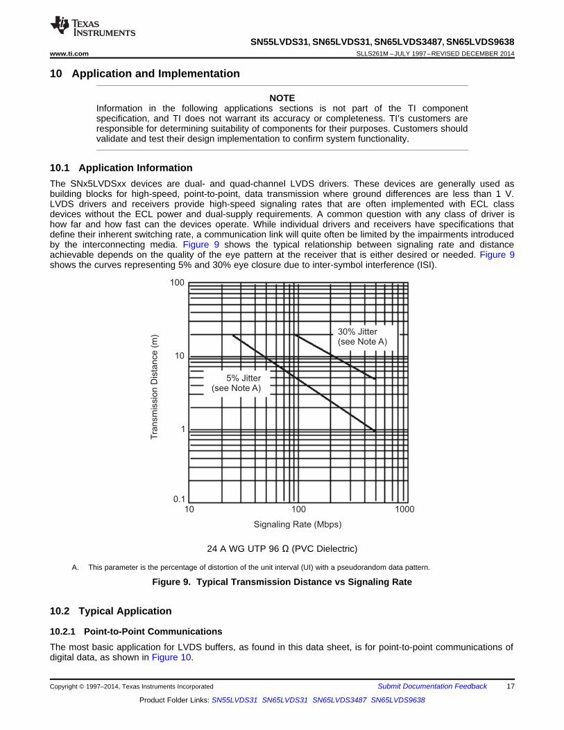
10.1 Application InformationThe SNx5LVDSxx devices are dual- and quad-channel LVDS drivers. These devices are generally used asbuilding blocks for high-speed, point-to-point, data transmission where ground differences are less than 1 V.LVDS drivers and receivers provide high-speed signaling rates that are often implemented with ECL classdevices without the ECL power and dual-supply requirements. A common question with any class of driver ishow far and how fast can the devices operate. While individual drivers and receivers have specifications thatdefine their inherent switching rate, a communication link will quite often be limited by the impairments introducedby the interconnecting media. Figure 9 shows the typical relationship between signaling rate and distanceachievable depends on the quality of the eye pattern at the receiver that is either desired or needed. Figure 9shows the curves representing 5% and 30% eye closure due to inter-symbol interference (ISI).
24 A WG UTP 96 Ω (PVC Dielectric)
A. This parameter is the percentage of distortion of the unit interval (UI) with a pseudorandom data pattern.
Figure 9. Typical Transmission Distance vs Signaling Rate
10.2 Typical Application
10.2.1 Point-to-Point CommunicationsThe most basic application for LVDS buffers, as found in this data sheet, is for point-to-point communications ofdigital data, as shown in Figure 10.
Copyright © 1997–2014, Texas Instruments Incorporated Submit Documentation Feedback 17
Product Folder Links: SN55LVDS31 SN65LVDS31 SN65LVDS3487 SN65LVDS9638
OUT+
OUT-
Receiver
IN+
IN-
100 Ω
100 Ω Differential T-Line
Driver
SN55LVDS31, SN65LVDS31, SN65LVDS3487, SN65LVDS9638SLLS261M –JULY 1997–REVISED DECEMBER 2014 www.ti.com
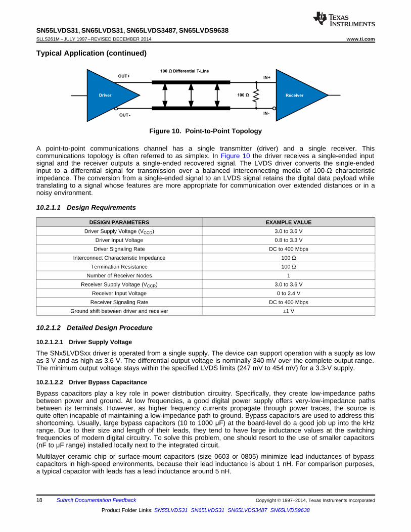
Typical Application (continued)
Figure 10. Point-to-Point Topology
A point-to-point communications channel has a single transmitter (driver) and a single receiver. Thiscommunications topology is often referred to as simplex. In Figure 10 the driver receives a single-ended inputsignal and the receiver outputs a single-ended recovered signal. The LVDS driver converts the single-endedinput to a differential signal for transmission over a balanced interconnecting media of 100-Ω characteristicimpedance. The conversion from a single-ended signal to an LVDS signal retains the digital data payload whiletranslating to a signal whose features are more appropriate for communication over extended distances or in anoisy environment.
10.2.1.1 Design Requirements
DESIGN PARAMETERS EXAMPLE VALUEDriver Supply Voltage (VCCD) 3.0 to 3.6 V
Driver Input Voltage 0.8 to 3.3 VDriver Signaling Rate DC to 400 Mbps
Interconnect Characteristic Impedance 100 ΩTermination Resistance 100 Ω
Number of Receiver Nodes 1Receiver Supply Voltage (VCCR) 3.0 to 3.6 V
Receiver Input Voltage 0 to 2.4 VReceiver Signaling Rate DC to 400 Mbps
Ground shift between driver and receiver ±1 V
10.2.1.2 Detailed Design Procedure
10.2.1.2.1 Driver Supply Voltage
The SNx5LVDSxx driver is operated from a single supply. The device can support operation with a supply as lowas 3 V and as high as 3.6 V. The differential output voltage is nominally 340 mV over the complete output range.The minimum output voltage stays within the specified LVDS limits (247 mV to 454 mV) for a 3.3-V supply.
10.2.1.2.2 Driver Bypass Capacitance
Bypass capacitors play a key role in power distribution circuitry. Specifically, they create low-impedance pathsbetween power and ground. At low frequencies, a good digital power supply offers very-low-impedance pathsbetween its terminals. However, as higher frequency currents propagate through power traces, the source isquite often incapable of maintaining a low-impedance path to ground. Bypass capacitors are used to address thisshortcoming. Usually, large bypass capacitors (10 to 1000 μF) at the board-level do a good job up into the kHzrange. Due to their size and length of their leads, they tend to have large inductance values at the switchingfrequencies of modern digital circuitry. To solve this problem, one should resort to the use of smaller capacitors(nF to μF range) installed locally next to the integrated circuit.
Multilayer ceramic chip or surface-mount capacitors (size 0603 or 0805) minimize lead inductances of bypasscapacitors in high-speed environments, because their lead inductance is about 1 nH. For comparison purposes,a typical capacitor with leads has a lead inductance around 5 nH.
18 Submit Documentation Feedback Copyright © 1997–2014, Texas Instruments Incorporated
Product Folder Links: SN55LVDS31 SN65LVDS31 SN65LVDS3487 SN65LVDS9638
3.3 V
0.1 F 0.001 F
LVDS1A
C 200 ps 0.001 F0.2V
æ ö= ´ = mç ÷
è ø
Maximum Step Change Supply Currentchip Rise Time
Maximum Power Supply Noise
IC T
V
Dæ ö= ´ç ÷Dè ø
SN55LVDS31, SN65LVDS31, SN65LVDS3487, SN65LVDS9638www.ti.com SLLS261M –JULY 1997–REVISED DECEMBER 2014
The value of the bypass capacitors used locally with LVDS chips can be determined by the following formulaaccording to Johnson, equations 8.18 to 8.21. A conservative rise time of 200 ps and a worst-case change insupply current of 1 A covers the whole range of LVDS devices offered by Texas Instruments. In this example, themaximum power supply noise tolerated is 200 mV; however, this figure varies depending on the noise budgetavailable in your design. (1)
(1)
(2)
The following example lowers lead inductance and covers intermediate frequencies between the board-levelcapacitor (>10 µF) and the value of capacitance found above (0.001 µF). You should place the smallest value ofcapacitance as close as possible to the chip.
Figure 11. Recommended LVDS Bypass Capacitor Layout
10.2.1.2.3 Driver Output Voltage
The SNx5LVDSxx driver output is a 1.2-V common-mode voltage, with a nominal differential output signal of 340mV. This 340 mV is the absolute value of the differential swing (VOD = |V+ – V–|). The peak-to-peak differentialvoltage is twice this value, or 680 mV.
10.2.1.2.4 Interconnecting Media
The physical communication channel between the driver and the receiver may be any balanced paired metalconductors meeting the requirements of the LVDS standard, the key points which will be included here. Thismedia may be a twisted pair, twinax, flat ribbon cable, or PCB traces. The nominal characteristic impedance ofthe interconnect should be between 100 Ω and 120 Ω with a variation of no more than 10% (90 Ω to 132 Ω).
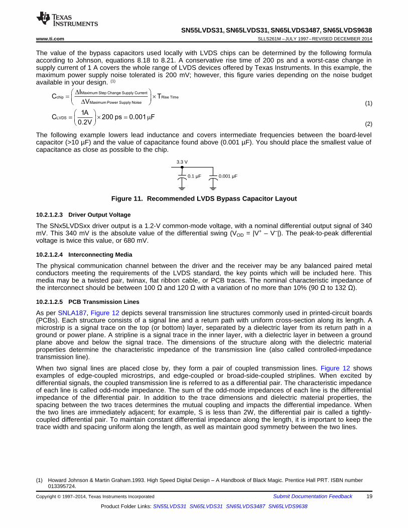
10.2.1.2.5 PCB Transmission Lines
As per SNLA187, Figure 12 depicts several transmission line structures commonly used in printed-circuit boards(PCBs). Each structure consists of a signal line and a return path with uniform cross-section along its length. Amicrostrip is a signal trace on the top (or bottom) layer, separated by a dielectric layer from its return path in aground or power plane. A stripline is a signal trace in the inner layer, with a dielectric layer in between a groundplane above and below the signal trace. The dimensions of the structure along with the dielectric materialproperties determine the characteristic impedance of the transmission line (also called controlled-impedancetransmission line).
When two signal lines are placed close by, they form a pair of coupled transmission lines. Figure 12 showsexamples of edge-coupled microstrips, and edge-coupled or broad-side-coupled striplines. When excited bydifferential signals, the coupled transmission line is referred to as a differential pair. The characteristic impedanceof each line is called odd-mode impedance. The sum of the odd-mode impedances of each line is the differentialimpedance of the differential pair. In addition to the trace dimensions and dielectric material properties, thespacing between the two traces determines the mutual coupling and impacts the differential impedance. Whenthe two lines are immediately adjacent; for example, S is less than 2W, the differential pair is called a tightly-coupled differential pair. To maintain constant differential impedance along the length, it is important to keep thetrace width and spacing uniform along the length, as well as maintain good symmetry between the two lines.
(1) Howard Johnson & Martin Graham.1993. High Speed Digital Design – A Handbook of Black Magic. Prentice Hall PRT. ISBN number013395724.
Copyright © 1997–2014, Texas Instruments Incorporated Submit Documentation Feedback 19
Product Folder Links: SN55LVDS31 SN65LVDS31 SN65LVDS3487 SN65LVDS9638
Single-Ended Microstrip
][ ++=
TW
HZ
8.0r
98.5ln
41.1
870
Edge-Coupled Edge-Coupled
Differential Microstrip
][ ×−××=×−
H
S
diff eZZ96.0
0 48.012
Single-Ended Stripline
( )( ) ][ +
+=
TW
THZ
8.0r
29.1ln
600
Differential Stripline
][ −××=×−
H
S
diff eZZ9.2
0 347.012
WW
H
H
T
T
H
S
G
W W
S G
H
H
H
S
H
Broad-Side Coupled StriplinesCo-Planar Coupled Microstrips
S
W
SN55LVDS31, SN65LVDS31, SN65LVDS3487, SN65LVDS9638SLLS261M –JULY 1997–REVISED DECEMBER 2014 www.ti.com
Figure 12. Controlled-Impedance Transmission Lines
10.2.1.2.6 Termination Resistor
As shown earlier, an LVDS communication channel employs a current source driving a transmission line which isterminated with a resistive load. This load serves to convert the transmitted current into a voltage at the receiverinput. To ensure incident wave switching (which is necessary to operate the channel at the highest signalingrate), the termination resistance should be matched to the characteristic impedance of the transmission line. Thedesigner should ensure that the termination resistance is within 10% of the nominal media characteristicimpedance. If the transmission line is targeted for 100-Ω impedance, the termination resistance should bebetween 90 and 110 Ω.
The line termination resistance should be located as close as possible to the receiver, thereby minimizing thestub length from the resistor to the receiver. The limiting case would be to incorporate the termination resistorinto the receiver, which is exactly what is offered with a device like the SN65LVDT386. The SN65LVDT386provides all the functionality and performance of the SN65LVDT386 receiver, with the added feature of anintegrated termination load.
While we talk in this section about point-to-point communications, a word of caution is useful when a multidroptopology is used. In such topologies, line termination resistors are to be located only at the end(s) of thetransmission line. In such an environment, SN65LVDT386 receivers could be used for loads branching off themain bus with an SN65LVDT386 used only at the bus end.
10.2.1.2.7 Driver NC Pins
NC (not connected) pins are pins where the die is not physically connected to the lead frame and package. Foroptimum thermal performance, a good rule of thumb is to ground the NC pins at the board level.
20 Submit Documentation Feedback Copyright © 1997–2014, Texas Instruments Incorporated
Product Folder Links: SN55LVDS31 SN65LVDS31 SN65LVDS3487 SN65LVDS9638
SN55LVDS31, SN65LVDS31, SN65LVDS3487, SN65LVDS9638www.ti.com SLLS261M –JULY 1997–REVISED DECEMBER 2014
10.2.1.3 Application Curve
Figure 13. Typical Driver Output Eye Pattern in Point-to-Point System
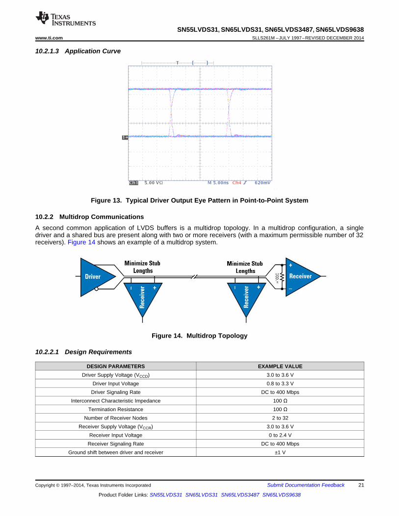
10.2.2 Multidrop CommunicationsA second common application of LVDS buffers is a multidrop topology. In a multidrop configuration, a singledriver and a shared bus are present along with two or more receivers (with a maximum permissible number of 32receivers). Figure 14 shows an example of a multidrop system.
Figure 14. Multidrop Topology
10.2.2.1 Design Requirements
DESIGN PARAMETERS EXAMPLE VALUEDriver Supply Voltage (VCCD) 3.0 to 3.6 V
Driver Input Voltage 0.8 to 3.3 VDriver Signaling Rate DC to 400 Mbps
Interconnect Characteristic Impedance 100 ΩTermination Resistance 100 Ω
Number of Receiver Nodes 2 to 32Receiver Supply Voltage (VCCR) 3.0 to 3.6 V
Receiver Input Voltage 0 to 2.4 VReceiver Signaling Rate DC to 400 Mbps
Ground shift between driver and receiver ±1 V
Copyright © 1997–2014, Texas Instruments Incorporated Submit Documentation Feedback 21
Product Folder Links: SN55LVDS31 SN65LVDS31 SN65LVDS3487 SN65LVDS9638
SN55LVDS31, SN65LVDS31, SN65LVDS3487, SN65LVDS9638SLLS261M –JULY 1997–REVISED DECEMBER 2014 www.ti.com
10.2.2.2 Detailed Design Procedure
10.2.2.2.1 Interconnecting Media
The interconnect in a multidrop system differs considerably from a point-to-point system. While point-to-pointinterconnects are straightforward and well understood, the bus type architecture encountered with multidropsystems requires more careful attention. We will use Figure 14 above to explore these details.
The most basic multidrop system would include a single driver, located at a bus origin, with multiple receivernodes branching off the main line, and a final receiver at the end of the transmission line, co-located with a bustermination resistor. While this would be the most basic multidrop system, it has several considerations not yetexplored.
The location of the transmitter at one bus end allows the design concerns to be simplified, but this comes at thecost of flexibility. With a transmitter located at the origin, a single bus termination at the far-end is required. Thefar-end termination absorbs the incident traveling wave. The flexibility lost with this arrangement is thus: if thesingle transmitter needed to be relocated on the bus, at any location other than the origin, we would be facedwith a bus with one open-circuited end, and one properly terminated end. Locating the transmitter say in themiddle of the bus may be desired to reduce (by ½) the maximum flight time from the transmitter to receiver.
Another new feature in Figure 14 is clear in that every node branching off the main line results in stubs. Thestubs should be minimized in any case, but have the unintended effect of locally changing the loaded impedanceof the bus.
To a good approximation, the characteristic transmission line impedance seen into any cut point in the unloadedmultipoint or multidrop bus is defined by √L/C, where L is the inductance per unit length and C is the capacitanceper unit length. As capacitance is added to the bus in the form of devices and interconnections, the buscharacteristic impedance is lowered. This may result in signal reflections from the impedance mismatch betweenthe unloaded and loaded segments of the bus.
If the number of loads is constant and can be distributed evenly along the line, reflections can be reduced bychanging the bus termination resistors to match the loaded characteristic impedance. Normally, the number ofloads are not constant or distributed evenly and the reflections resulting from any mismatching should beaccounted for in the noise budget.
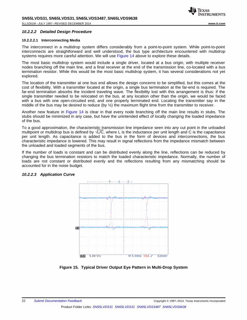
10.2.2.3 Application Curve
Figure 15. Typical Driver Output Eye Pattern in Multi-Drop System
22 Submit Documentation Feedback Copyright © 1997–2014, Texas Instruments Incorporated
Product Folder Links: SN55LVDS31 SN65LVDS31 SN65LVDS3487 SN65LVDS9638
SN55LVDS31, SN65LVDS31, SN65LVDS3487, SN65LVDS9638www.ti.com SLLS261M –JULY 1997–REVISED DECEMBER 2014
11 Power Supply Recommendations
The LVDS drivers in this data sheet are designed to operate from a single power supply, with supply voltages inthe range of 3.0 V to 3.6 V. In a typical application, a driver and a receiver may be on separate boards or evenseparate equipment. In these cases, separate supplies would be used at each location. The expected groundpotential difference between the driver power supply and the receiver power supply would be less than |±1 V|.Board-level and local device-level bypass capacitance should be used and are covered in Driver BypassCapacitance.
12 Layout
12.1 Layout Guidelines
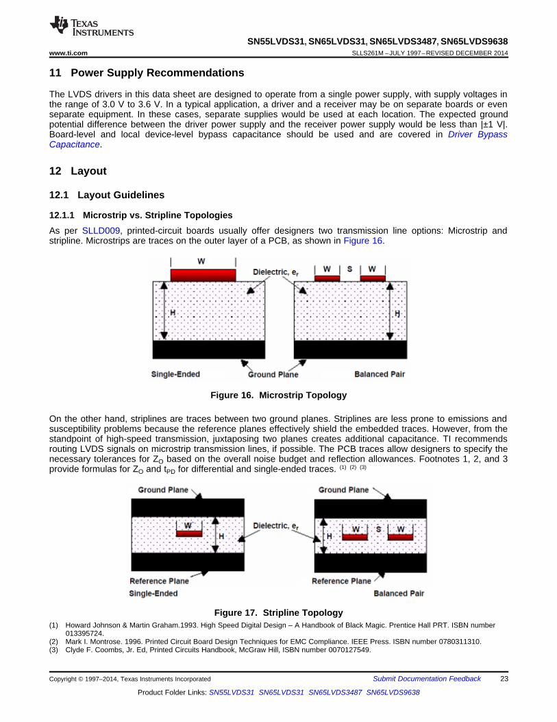
12.1.1 Microstrip vs. Stripline TopologiesAs per SLLD009, printed-circuit boards usually offer designers two transmission line options: Microstrip andstripline. Microstrips are traces on the outer layer of a PCB, as shown in Figure 16.
Figure 16. Microstrip Topology
On the other hand, striplines are traces between two ground planes. Striplines are less prone to emissions andsusceptibility problems because the reference planes effectively shield the embedded traces. However, from thestandpoint of high-speed transmission, juxtaposing two planes creates additional capacitance. TI recommendsrouting LVDS signals on microstrip transmission lines, if possible. The PCB traces allow designers to specify thenecessary tolerances for ZO based on the overall noise budget and reflection allowances. Footnotes 1, 2, and 3provide formulas for ZO and tPD for differential and single-ended traces. (1) (2) (3)
Figure 17. Stripline Topology(1) Howard Johnson & Martin Graham.1993. High Speed Digital Design – A Handbook of Black Magic. Prentice Hall PRT. ISBN number
013395724.(2) Mark I. Montrose. 1996. Printed Circuit Board Design Techniques for EMC Compliance. IEEE Press. ISBN number 0780311310.(3) Clyde F. Coombs, Jr. Ed, Printed Circuits Handbook, McGraw Hill, ISBN number 0070127549.
Copyright © 1997–2014, Texas Instruments Incorporated Submit Documentation Feedback 23
Product Folder Links: SN55LVDS31 SN65LVDS31 SN65LVDS3487 SN65LVDS9638
Layer 1: Routed Plane (LVDS Signals)
Layer 2: Ground Plane
Layer 3: Power Plane
Layer 4: Ground Plane
Layer 5: Ground Plane
Layer 6: Routed Plane (TTL Signals)
Layer 1: Routed Plane (LVDS Signals)
Layer 2: Ground Plane
Layer 3: Power Plane
Layer 4: Routed Plane (TTL/CMOS Signals)
SN55LVDS31, SN65LVDS31, SN65LVDS3487, SN65LVDS9638SLLS261M –JULY 1997–REVISED DECEMBER 2014 www.ti.com
Layout Guidelines (continued)12.1.2 Dielectric Type and Board ConstructionThe speeds at which signals travel across the board dictates the choice of dielectric. FR-4, or equivalent, usuallyprovides adequate performance for use with LVDS signals. If rise or fall times of TTL/CMOS signals are lessthan 500 ps, empirical results indicate that a material with a dielectric constant near 3.4, such as Rogers™ 4350or Nelco N4000-13 is better suited. Once the designer chooses the dielectric, there are several parameterspertaining to the board construction that can affect performance. The following set of guidelines were developedexperimentally through several designs involving LVDS devices:• Copper weight: 15 g or 1/2 oz start, plated to 30 g or 1 oz• All exposed circuitry should be solder-plated (60/40) to 7.62 μm or 0.0003 in (minimum).• Copper plating should be 25.4 μm or 0.001 in (minimum) in plated-through-holes.• Solder mask over bare copper with solder hot-air leveling
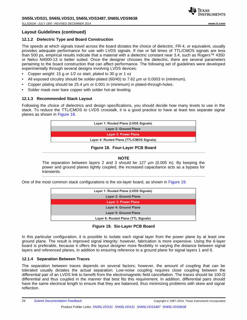
12.1.3 Recommended Stack LayoutFollowing the choice of dielectrics and design specifications, you should decide how many levels to use in thestack. To reduce the TTL/CMOS to LVDS crosstalk, it is a good practice to have at least two separate signalplanes as shown in Figure 18.
Figure 18. Four-Layer PCB Board
NOTEThe separation between layers 2 and 3 should be 127 μm (0.005 in). By keeping thepower and ground planes tightly coupled, the increased capacitance acts as a bypass fortransients.
One of the most common stack configurations is the six-layer board, as shown in Figure 19.
Figure 19. Six-Layer PCB Board
In this particular configuration, it is possible to isolate each signal layer from the power plane by at least oneground plane. The result is improved signal integrity; however, fabrication is more expensive. Using the 6-layerboard is preferable, because it offers the layout designer more flexibility in varying the distance between signallayers and referenced planes, in addition to ensuring reference to a ground plane for signal layers 1 and 6.
12.1.4 Separation Between TracesThe separation between traces depends on several factors; however, the amount of coupling that can betolerated usually dictates the actual separation. Low-noise coupling requires close coupling between thedifferential pair of an LVDS link to benefit from the electromagnetic field cancellation. The traces should be 100-Ωdifferential and thus coupled in the manner that best fits this requirement. In addition, differential pairs shouldhave the same electrical length to ensure that they are balanced, thus minimizing problems with skew and signalreflection.
24 Submit Documentation Feedback Copyright © 1997–2014, Texas Instruments Incorporated
Product Folder Links: SN55LVDS31 SN65LVDS31 SN65LVDS3487 SN65LVDS9638
Layer 1
Layer 6
LVDS
Pair
TTL/CMOS
Trace
W
W
W
S = Minimum Spacing as Defined by PCB Vender
≥2 W
Differential Traces
Single-Ended Traces
SN55LVDS31, SN65LVDS31, SN65LVDS3487, SN65LVDS9638www.ti.com SLLS261M –JULY 1997–REVISED DECEMBER 2014
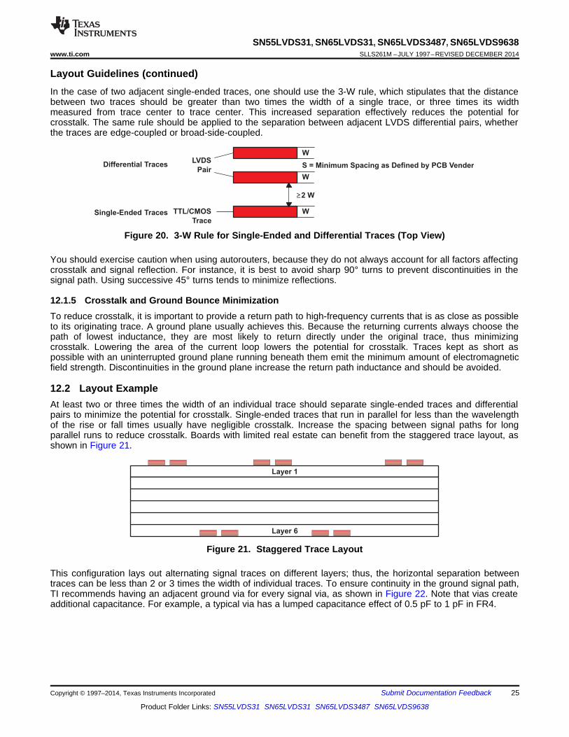
Layout Guidelines (continued)In the case of two adjacent single-ended traces, one should use the 3-W rule, which stipulates that the distancebetween two traces should be greater than two times the width of a single trace, or three times its widthmeasured from trace center to trace center. This increased separation effectively reduces the potential forcrosstalk. The same rule should be applied to the separation between adjacent LVDS differential pairs, whetherthe traces are edge-coupled or broad-side-coupled.
Figure 20. 3-W Rule for Single-Ended and Differential Traces (Top View)
You should exercise caution when using autorouters, because they do not always account for all factors affectingcrosstalk and signal reflection. For instance, it is best to avoid sharp 90° turns to prevent discontinuities in thesignal path. Using successive 45° turns tends to minimize reflections.
12.1.5 Crosstalk and Ground Bounce MinimizationTo reduce crosstalk, it is important to provide a return path to high-frequency currents that is as close as possibleto its originating trace. A ground plane usually achieves this. Because the returning currents always choose thepath of lowest inductance, they are most likely to return directly under the original trace, thus minimizingcrosstalk. Lowering the area of the current loop lowers the potential for crosstalk. Traces kept as short aspossible with an uninterrupted ground plane running beneath them emit the minimum amount of electromagneticfield strength. Discontinuities in the ground plane increase the return path inductance and should be avoided.
12.2 Layout ExampleAt least two or three times the width of an individual trace should separate single-ended traces and differentialpairs to minimize the potential for crosstalk. Single-ended traces that run in parallel for less than the wavelengthof the rise or fall times usually have negligible crosstalk. Increase the spacing between signal paths for longparallel runs to reduce crosstalk. Boards with limited real estate can benefit from the staggered trace layout, asshown in Figure 21.
Figure 21. Staggered Trace Layout
This configuration lays out alternating signal traces on different layers; thus, the horizontal separation betweentraces can be less than 2 or 3 times the width of individual traces. To ensure continuity in the ground signal path,TI recommends having an adjacent ground via for every signal via, as shown in Figure 22. Note that vias createadditional capacitance. For example, a typical via has a lumped capacitance effect of 0.5 pF to 1 pF in FR4.
Copyright © 1997–2014, Texas Instruments Incorporated Submit Documentation Feedback 25
Product Folder Links: SN55LVDS31 SN65LVDS31 SN65LVDS3487 SN65LVDS9638
Signal Trace
Uninterrupted Ground Plane
Ground via
Signal via
Signal Trace
Uninterrupted Ground Plane
SN55LVDS31, SN65LVDS31, SN65LVDS3487, SN65LVDS9638SLLS261M –JULY 1997–REVISED DECEMBER 2014 www.ti.com
Layout Example (continued)
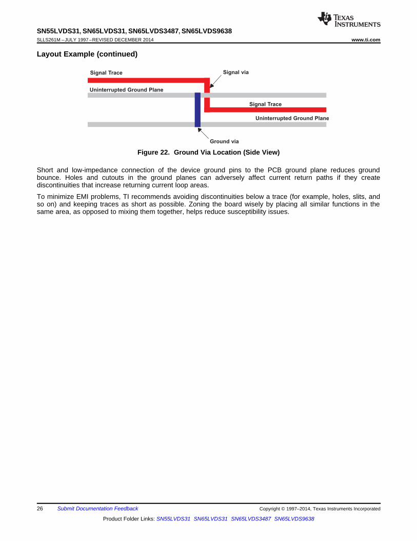
Figure 22. Ground Via Location (Side View)
Short and low-impedance connection of the device ground pins to the PCB ground plane reduces groundbounce. Holes and cutouts in the ground planes can adversely affect current return paths if they creatediscontinuities that increase returning current loop areas.
To minimize EMI problems, TI recommends avoiding discontinuities below a trace (for example, holes, slits, andso on) and keeping traces as short as possible. Zoning the board wisely by placing all similar functions in thesame area, as opposed to mixing them together, helps reduce susceptibility issues.
26 Submit Documentation Feedback Copyright © 1997–2014, Texas Instruments Incorporated
Product Folder Links: SN55LVDS31 SN65LVDS31 SN65LVDS3487 SN65LVDS9638
SN55LVDS31, SN65LVDS31, SN65LVDS3487, SN65LVDS9638www.ti.com SLLS261M –JULY 1997–REVISED DECEMBER 2014
13 Device and Documentation Support
13.1 Device Support
13.1.1 Third-Party Products DisclaimerTI'S PUBLICATION OF INFORMATION REGARDING THIRD-PARTY PRODUCTS OR SERVICES DOES NOTCONSTITUTE AN ENDORSEMENT REGARDING THE SUITABILITY OF SUCH PRODUCTS OR SERVICESOR A WARRANTY, REPRESENTATION OR ENDORSEMENT OF SUCH PRODUCTS OR SERVICES, EITHERALONE OR IN COMBINATION WITH ANY TI PRODUCT OR SERVICE.
13.1.2 Other LVDS ProductsFor other products and application notes in the LVDS and LVDM product families visit our Web site athttp://www.ti.com/sc/datatran.
13.2 Documentation Support
13.2.1 Related InformationIBIS modeling is available for this device. Contact the local TI sales office or the TI Web site at www.ti.com formore information.
For more application guidelines, see the following documents:• Low-Voltage Differential Signaling Design Notes (SLLA014)• Interface Circuits for TIA/EIA-644 (LVDS) (SLLA038)• Reducing EMI With LVDS (SLLA030)• Slew Rate Control of LVDS Circuits (SLLA034)• Using an LVDS Receiver With RS-422 Data (SLLA031)• Evaluating the LVDS EVM (SLLA033)
13.3 Related LinksTable 4 lists quick access links. Categories include technical documents, support and community resources,tools and software, and quick access to sample or buy.
Table 4. Related LinksTECHNICAL TOOLS & SUPPORT &PARTS PRODUCT FOLDER SAMPLE & BUY DOCUMENTS SOFTWARE COMMUNITY
SN55LVDS31 Click here Click here Click here Click here Click hereSN65LVDS31 Click here Click here Click here Click here Click here
SN65LVDS3487 Click here Click here Click here Click here Click hereSN65LVDS9638 Click here Click here Click here Click here Click here
13.4 TrademarksPowerPAD is a trademark of Texas Instruments.Rogers is a trademark of Rogers Corporation.All other trademarks are the property of their respective owners.
13.5 Electrostatic Discharge CautionThese devices have limited built-in ESD protection. The leads should be shorted together or the device placed in conductive foamduring storage or handling to prevent electrostatic damage to the MOS gates.
13.6 GlossarySLYZ022 — TI Glossary.
This glossary lists and explains terms, acronyms, and definitions.
Copyright © 1997–2014, Texas Instruments Incorporated Submit Documentation Feedback 27
Product Folder Links: SN55LVDS31 SN65LVDS31 SN65LVDS3487 SN65LVDS9638
SN55LVDS31, SN65LVDS31, SN65LVDS3487, SN65LVDS9638SLLS261M –JULY 1997–REVISED DECEMBER 2014 www.ti.com
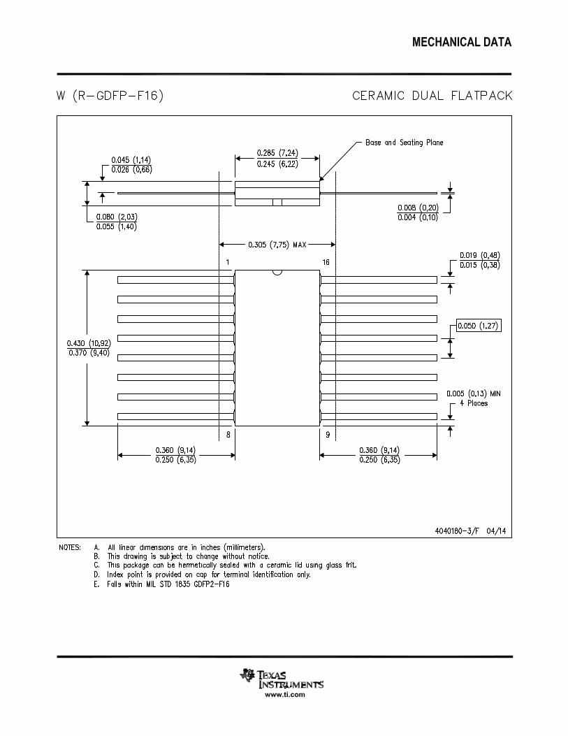
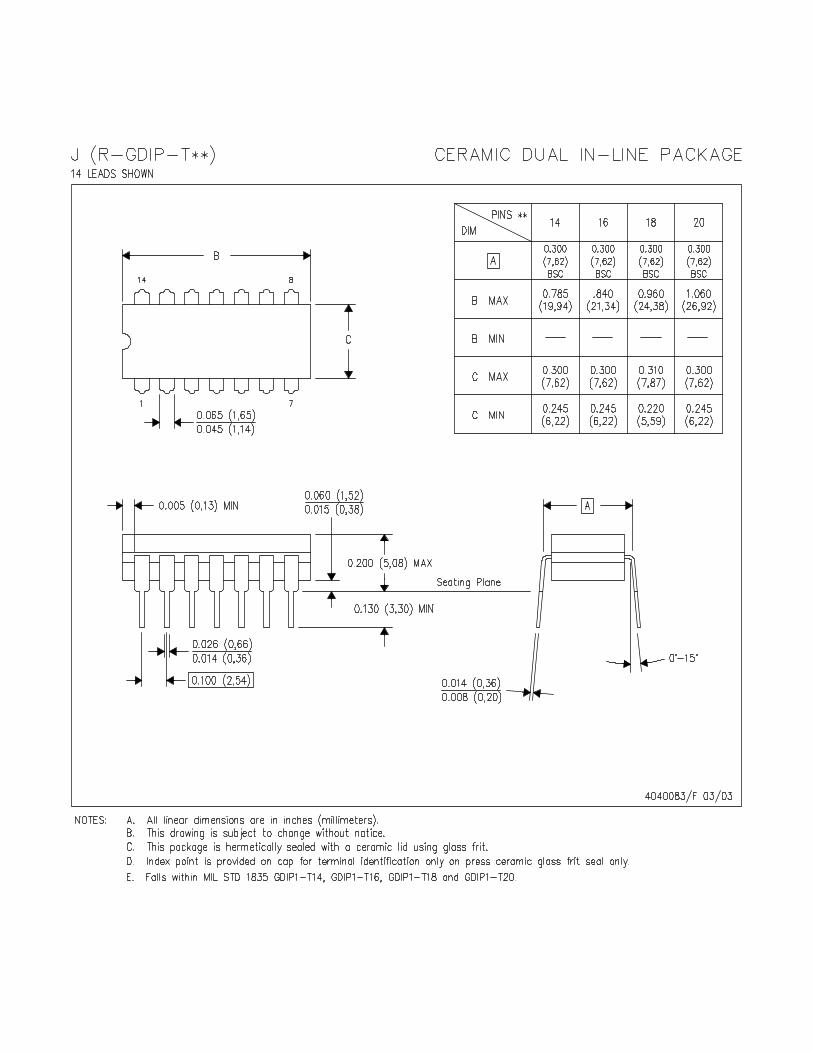
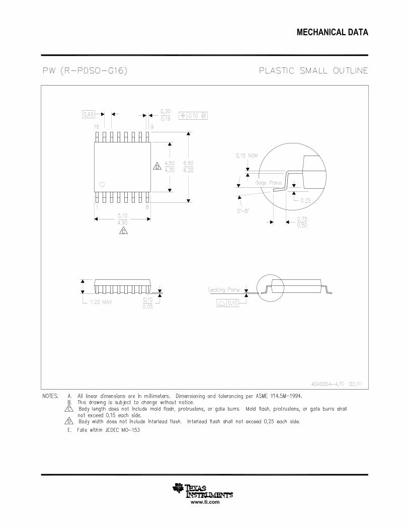
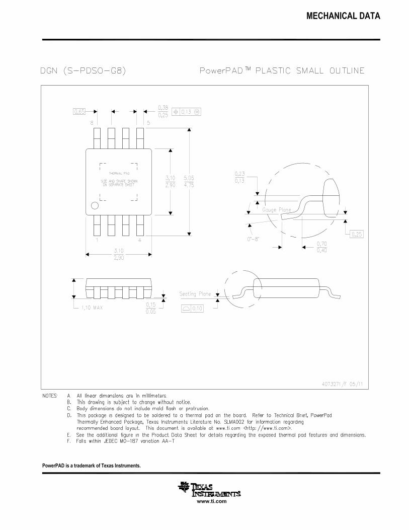
14 Mechanical, Packaging, and Orderable InformationThe following pages include mechanical, packaging, and orderable information. This information is the mostcurrent data available for the designated devices. This data is subject to change without notice and revision ofthis document. For browser-based versions of this data sheet, refer to the left-hand navigation.
28 Submit Documentation Feedback Copyright © 1997–2014, Texas Instruments Incorporated
Product Folder Links: SN55LVDS31 SN65LVDS31 SN65LVDS3487 SN65LVDS9638
PACKAGE OPTION ADDENDUM
www.ti.com 17-Mar-2017
Addendum-Page 1
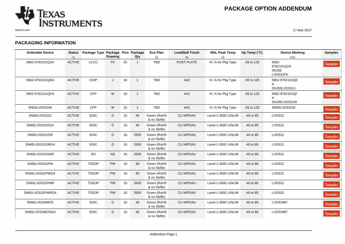
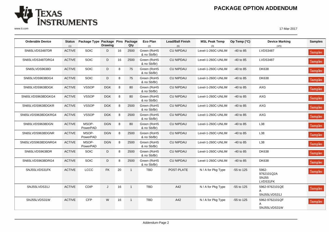
PACKAGING INFORMATION
Orderable Device Status(1)
Package Type PackageDrawing
Pins PackageQty
Eco Plan(2)
Lead/Ball Finish(6)
MSL Peak Temp(3)
Op Temp (°C) Device Marking(4/5)
Samples
5962-9762101Q2A ACTIVE LCCC FK 20 1 TBD POST-PLATE N / A for Pkg Type -55 to 125 5962-9762101Q2ASNJ55LVDS31FK
5962-9762101QEA ACTIVE CDIP J 16 1 TBD A42 N / A for Pkg Type -55 to 125 5962-9762101QEASNJ55LVDS31J
5962-9762101QFA ACTIVE CFP W 16 1 TBD A42 N / A for Pkg Type -55 to 125 5962-9762101QFASNJ55LVDS31W
SN55LVDS31W ACTIVE CFP W 16 1 TBD A42 N / A for Pkg Type -55 to 125 SN55LVDS31W
SN65LVDS31D ACTIVE SOIC D 16 40 Green (RoHS& no Sb/Br)
CU NIPDAU Level-1-260C-UNLIM -40 to 85 LVDS31
SN65LVDS31DG4 ACTIVE SOIC D 16 40 Green (RoHS& no Sb/Br)
CU NIPDAU Level-1-260C-UNLIM -40 to 85 LVDS31
SN65LVDS31DR ACTIVE SOIC D 16 2500 Green (RoHS& no Sb/Br)
CU NIPDAU Level-1-260C-UNLIM -40 to 85 LVDS31
SN65LVDS31DRG4 ACTIVE SOIC D 16 2500 Green (RoHS& no Sb/Br)
CU NIPDAU Level-1-260C-UNLIM -40 to 85 LVDS31
SN65LVDS31NSR ACTIVE SO NS 16 2000 Green (RoHS& no Sb/Br)
CU NIPDAU Level-1-260C-UNLIM -40 to 85 LVDS31
SN65LVDS31PW ACTIVE TSSOP PW 16 90 Green (RoHS& no Sb/Br)
CU NIPDAU Level-1-260C-UNLIM -40 to 85 LVDS31
SN65LVDS31PWG4 ACTIVE TSSOP PW 16 90 Green (RoHS& no Sb/Br)
CU NIPDAU Level-1-260C-UNLIM -40 to 85 LVDS31
SN65LVDS31PWR ACTIVE TSSOP PW 16 2000 Green (RoHS& no Sb/Br)
CU NIPDAU Level-1-260C-UNLIM -40 to 85 LVDS31
SN65LVDS31PWRG4 ACTIVE TSSOP PW 16 2000 Green (RoHS& no Sb/Br)
CU NIPDAU Level-1-260C-UNLIM -40 to 85 LVDS31
SN65LVDS3487D ACTIVE SOIC D 16 40 Green (RoHS& no Sb/Br)
CU NIPDAU Level-1-260C-UNLIM -40 to 85 LVDS3487
SN65LVDS3487DG4 ACTIVE SOIC D 16 40 Green (RoHS& no Sb/Br)
CU NIPDAU Level-1-260C-UNLIM -40 to 85 LVDS3487
PACKAGE OPTION ADDENDUM
www.ti.com 17-Mar-2017
Addendum-Page 2
Orderable Device Status(1)
Package Type PackageDrawing
Pins PackageQty
Eco Plan(2)
Lead/Ball Finish(6)
MSL Peak Temp(3)
Op Temp (°C) Device Marking(4/5)
Samples
SN65LVDS3487DR ACTIVE SOIC D 16 2500 Green (RoHS& no Sb/Br)
CU NIPDAU Level-1-260C-UNLIM -40 to 85 LVDS3487
SN65LVDS3487DRG4 ACTIVE SOIC D 16 2500 Green (RoHS& no Sb/Br)
CU NIPDAU Level-1-260C-UNLIM -40 to 85 LVDS3487
SN65LVDS9638D ACTIVE SOIC D 8 75 Green (RoHS& no Sb/Br)
CU NIPDAU Level-1-260C-UNLIM -40 to 85 DK638
SN65LVDS9638DG4 ACTIVE SOIC D 8 75 Green (RoHS& no Sb/Br)
CU NIPDAU Level-1-260C-UNLIM -40 to 85 DK638
SN65LVDS9638DGK ACTIVE VSSOP DGK 8 80 Green (RoHS& no Sb/Br)
CU NIPDAU Level-1-260C-UNLIM -40 to 85 AXG
SN65LVDS9638DGKG4 ACTIVE VSSOP DGK 8 80 Green (RoHS& no Sb/Br)
CU NIPDAU Level-1-260C-UNLIM -40 to 85 AXG
SN65LVDS9638DGKR ACTIVE VSSOP DGK 8 2500 Green (RoHS& no Sb/Br)
CU NIPDAU Level-1-260C-UNLIM -40 to 85 AXG
SN65LVDS9638DGKRG4 ACTIVE VSSOP DGK 8 2500 Green (RoHS& no Sb/Br)
CU NIPDAU Level-1-260C-UNLIM -40 to 85 AXG
SN65LVDS9638DGN ACTIVE MSOP-PowerPAD
DGN 8 80 Green (RoHS& no Sb/Br)
CU NIPDAU Level-1-260C-UNLIM -40 to 85 L38
SN65LVDS9638DGNR ACTIVE MSOP-PowerPAD
DGN 8 2500 Green (RoHS& no Sb/Br)
CU NIPDAU Level-1-260C-UNLIM -40 to 85 L38
SN65LVDS9638DGNRG4 ACTIVE MSOP-PowerPAD
DGN 8 2500 Green (RoHS& no Sb/Br)
CU NIPDAU Level-1-260C-UNLIM -40 to 85 L38
SN65LVDS9638DR ACTIVE SOIC D 8 2500 Green (RoHS& no Sb/Br)
CU NIPDAU Level-1-260C-UNLIM -40 to 85 DK638
SN65LVDS9638DRG4 ACTIVE SOIC D 8 2500 Green (RoHS& no Sb/Br)
CU NIPDAU Level-1-260C-UNLIM -40 to 85 DK638
SNJ55LVDS31FK ACTIVE LCCC FK 20 1 TBD POST-PLATE N / A for Pkg Type -55 to 125 5962-9762101Q2ASNJ55LVDS31FK
SNJ55LVDS31J ACTIVE CDIP J 16 1 TBD A42 N / A for Pkg Type -55 to 125 5962-9762101QEASNJ55LVDS31J
SNJ55LVDS31W ACTIVE CFP W 16 1 TBD A42 N / A for Pkg Type -55 to 125 5962-9762101QFASNJ55LVDS31W
PACKAGE OPTION ADDENDUM
www.ti.com 17-Mar-2017
Addendum-Page 3
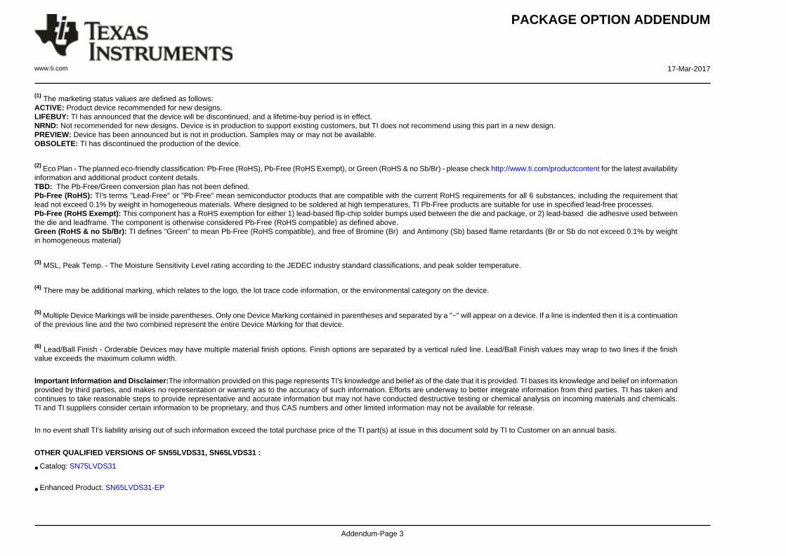
(1) The marketing status values are defined as follows:ACTIVE: Product device recommended for new designs.LIFEBUY: TI has announced that the device will be discontinued, and a lifetime-buy period is in effect.NRND: Not recommended for new designs. Device is in production to support existing customers, but TI does not recommend using this part in a new design.PREVIEW: Device has been announced but is not in production. Samples may or may not be available.OBSOLETE: TI has discontinued the production of the device.
(2) Eco Plan - The planned eco-friendly classification: Pb-Free (RoHS), Pb-Free (RoHS Exempt), or Green (RoHS & no Sb/Br) - please check http://www.ti.com/productcontent for the latest availabilityinformation and additional product content details.TBD: The Pb-Free/Green conversion plan has not been defined.Pb-Free (RoHS): TI's terms "Lead-Free" or "Pb-Free" mean semiconductor products that are compatible with the current RoHS requirements for all 6 substances, including the requirement thatlead not exceed 0.1% by weight in homogeneous materials. Where designed to be soldered at high temperatures, TI Pb-Free products are suitable for use in specified lead-free processes.Pb-Free (RoHS Exempt): This component has a RoHS exemption for either 1) lead-based flip-chip solder bumps used between the die and package, or 2) lead-based die adhesive used betweenthe die and leadframe. The component is otherwise considered Pb-Free (RoHS compatible) as defined above.Green (RoHS & no Sb/Br): TI defines "Green" to mean Pb-Free (RoHS compatible), and free of Bromine (Br) and Antimony (Sb) based flame retardants (Br or Sb do not exceed 0.1% by weightin homogeneous material)
(3) MSL, Peak Temp. - The Moisture Sensitivity Level rating according to the JEDEC industry standard classifications, and peak solder temperature.
(4) There may be additional marking, which relates to the logo, the lot trace code information, or the environmental category on the device.
(5) Multiple Device Markings will be inside parentheses. Only one Device Marking contained in parentheses and separated by a "~" will appear on a device. If a line is indented then it is a continuationof the previous line and the two combined represent the entire Device Marking for that device.
(6) Lead/Ball Finish - Orderable Devices may have multiple material finish options. Finish options are separated by a vertical ruled line. Lead/Ball Finish values may wrap to two lines if the finishvalue exceeds the maximum column width.
Important Information and Disclaimer:The information provided on this page represents TI's knowledge and belief as of the date that it is provided. TI bases its knowledge and belief on informationprovided by third parties, and makes no representation or warranty as to the accuracy of such information. Efforts are underway to better integrate information from third parties. TI has taken andcontinues to take reasonable steps to provide representative and accurate information but may not have conducted destructive testing or chemical analysis on incoming materials and chemicals.TI and TI suppliers consider certain information to be proprietary, and thus CAS numbers and other limited information may not be available for release.
In no event shall TI's liability arising out of such information exceed the total purchase price of the TI part(s) at issue in this document sold by TI to Customer on an annual basis.
OTHER QUALIFIED VERSIONS OF SN55LVDS31, SN65LVDS31 :
• Catalog: SN75LVDS31
• Enhanced Product: SN65LVDS31-EP
PACKAGE OPTION ADDENDUM
www.ti.com 17-Mar-2017
Addendum-Page 4
• Space: SN55LVDS31-SP
NOTE: Qualified Version Definitions:
• Catalog - TI's standard catalog product
• Enhanced Product - Supports Defense, Aerospace and Medical Applications
• Space - Radiation tolerant, ceramic packaging and qualified for use in Space-based application
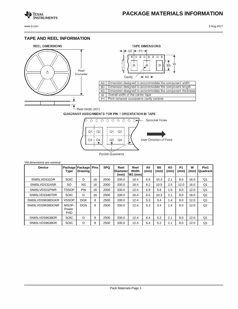
TAPE AND REEL INFORMATION
*All dimensions are nominal
Device PackageType
PackageDrawing
Pins SPQ ReelDiameter
(mm)
ReelWidth
W1 (mm)
A0(mm)
B0(mm)
K0(mm)
P1(mm)
W(mm)
Pin1Quadrant
SN65LVDS31DR SOIC D 16 2500 330.0 16.4 6.5 10.3 2.1 8.0 16.0 Q1
SN65LVDS31NSR SO NS 16 2000 330.0 16.4 8.2 10.5 2.5 12.0 16.0 Q1
SN65LVDS31PWR TSSOP PW 16 2000 330.0 12.4 6.9 5.6 1.6 8.0 12.0 Q1
SN65LVDS3487DR SOIC D 16 2500 330.0 16.4 6.5 10.3 2.1 8.0 16.0 Q1
SN65LVDS9638DGKR VSSOP DGK 8 2500 330.0 12.4 5.3 3.4 1.4 8.0 12.0 Q1
SN65LVDS9638DGNR MSOP-Power PAD
DGN 8 2500 330.0 12.4 5.3 3.4 1.4 8.0 12.0 Q1
SN65LVDS9638DR SOIC D 8 2500 330.0 12.4 6.4 5.2 2.1 8.0 12.0 Q1
SN65LVDS9638DR SOIC D 8 2500 330.0 12.4 6.4 5.2 2.1 8.0 12.0 Q1
PACKAGE MATERIALS INFORMATION
www.ti.com 3-Aug-2017
Pack Materials-Page 1
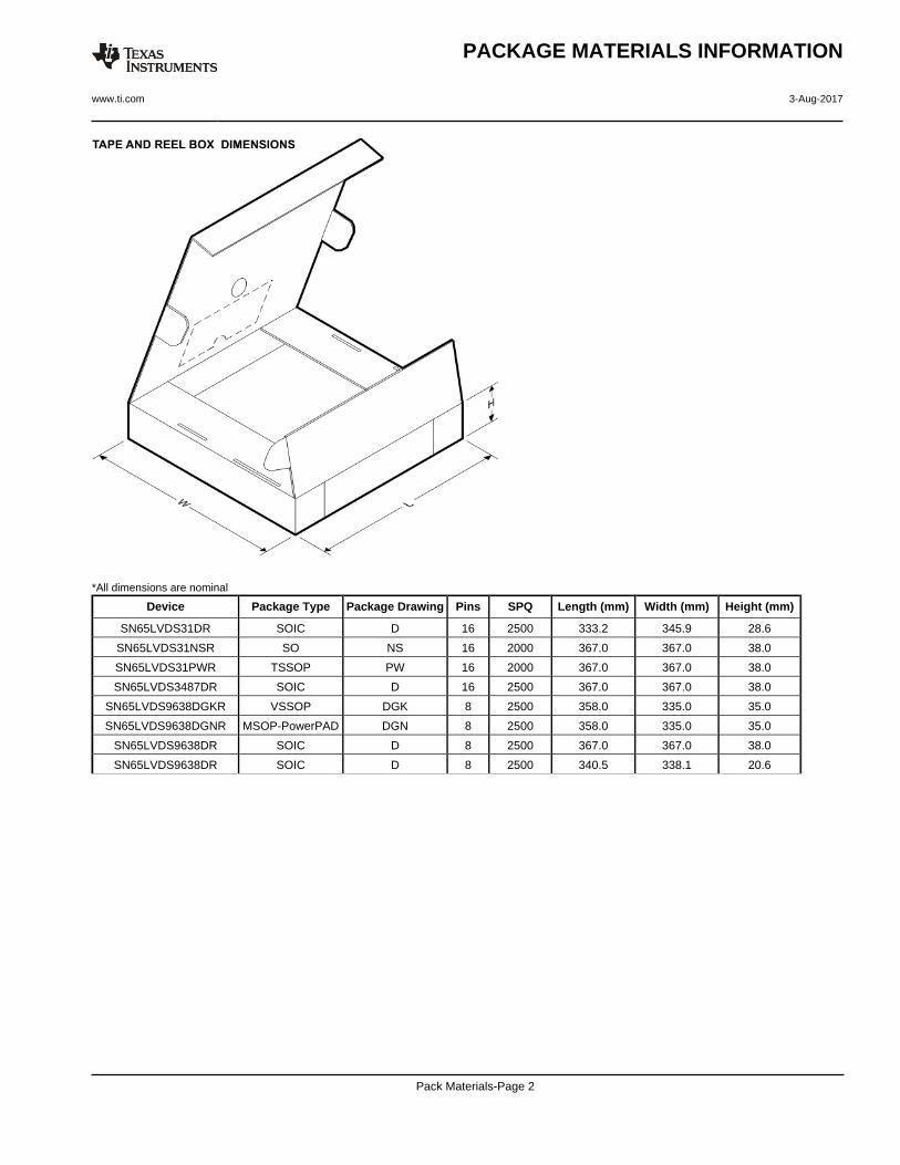
*All dimensions are nominal
Device Package Type Package Drawing Pins SPQ Length (mm) Width (mm) Height (mm)
SN65LVDS31DR SOIC D 16 2500 333.2 345.9 28.6
SN65LVDS31NSR SO NS 16 2000 367.0 367.0 38.0
SN65LVDS31PWR TSSOP PW 16 2000 367.0 367.0 38.0
SN65LVDS3487DR SOIC D 16 2500 367.0 367.0 38.0
SN65LVDS9638DGKR VSSOP DGK 8 2500 358.0 335.0 35.0
SN65LVDS9638DGNR MSOP-PowerPAD DGN 8 2500 358.0 335.0 35.0
SN65LVDS9638DR SOIC D 8 2500 367.0 367.0 38.0
SN65LVDS9638DR SOIC D 8 2500 340.5 338.1 20.6
PACKAGE MATERIALS INFORMATION
www.ti.com 3-Aug-2017
Pack Materials-Page 2
IMPORTANT NOTICE
Texas Instruments Incorporated (TI) reserves the right to make corrections, enhancements, improvements and other changes to itssemiconductor products and services per JESD46, latest issue, and to discontinue any product or service per JESD48, latest issue. Buyersshould obtain the latest relevant information before placing orders and should verify that such information is current and complete.TI’s published terms of sale for semiconductor products (http://www.ti.com/sc/docs/stdterms.htm) apply to the sale of packaged integratedcircuit products that TI has qualified and released to market. Additional terms may apply to the use or sale of other types of TI products andservices.Reproduction of significant portions of TI information in TI data sheets is permissible only if reproduction is without alteration and isaccompanied by all associated warranties, conditions, limitations, and notices. TI is not responsible or liable for such reproduceddocumentation. Information of third parties may be subject to additional restrictions. Resale of TI products or services with statementsdifferent from or beyond the parameters stated by TI for that product or service voids all express and any implied warranties for theassociated TI product or service and is an unfair and deceptive business practice. TI is not responsible or liable for any such statements.Buyers and others who are developing systems that incorporate TI products (collectively, “Designers”) understand and agree that Designersremain responsible for using their independent analysis, evaluation and judgment in designing their applications and that Designers havefull and exclusive responsibility to assure the safety of Designers' applications and compliance of their applications (and of all TI productsused in or for Designers’ applications) with all applicable regulations, laws and other applicable requirements. Designer represents that, withrespect to their applications, Designer has all the necessary expertise to create and implement safeguards that (1) anticipate dangerousconsequences of failures, (2) monitor failures and their consequences, and (3) lessen the likelihood of failures that might cause harm andtake appropriate actions. Designer agrees that prior to using or distributing any applications that include TI products, Designer willthoroughly test such applications and the functionality of such TI products as used in such applications.TI’s provision of technical, application or other design advice, quality characterization, reliability data or other services or information,including, but not limited to, reference designs and materials relating to evaluation modules, (collectively, “TI Resources”) are intended toassist designers who are developing applications that incorporate TI products; by downloading, accessing or using TI Resources in anyway, Designer (individually or, if Designer is acting on behalf of a company, Designer’s company) agrees to use any particular TI Resourcesolely for this purpose and subject to the terms of this Notice.TI’s provision of TI Resources does not expand or otherwise alter TI’s applicable published warranties or warranty disclaimers for TIproducts, and no additional obligations or liabilities arise from TI providing such TI Resources. TI reserves the right to make corrections,enhancements, improvements and other changes to its TI Resources. TI has not conducted any testing other than that specificallydescribed in the published documentation for a particular TI Resource.Designer is authorized to use, copy and modify any individual TI Resource only in connection with the development of applications thatinclude the TI product(s) identified in such TI Resource. NO OTHER LICENSE, EXPRESS OR IMPLIED, BY ESTOPPEL OR OTHERWISETO ANY OTHER TI INTELLECTUAL PROPERTY RIGHT, AND NO LICENSE TO ANY TECHNOLOGY OR INTELLECTUAL PROPERTYRIGHT OF TI OR ANY THIRD PARTY IS GRANTED HEREIN, including but not limited to any patent right, copyright, mask work right, orother intellectual property right relating to any combination, machine, or process in which TI products or services are used. Informationregarding or referencing third-party products or services does not constitute a license to use such products or services, or a warranty orendorsement thereof. Use of TI Resources may require a license from a third party under the patents or other intellectual property of thethird party, or a license from TI under the patents or other intellectual property of TI.TI RESOURCES ARE PROVIDED “AS IS” AND WITH ALL FAULTS. TI DISCLAIMS ALL OTHER WARRANTIES ORREPRESENTATIONS, EXPRESS OR IMPLIED, REGARDING RESOURCES OR USE THEREOF, INCLUDING BUT NOT LIMITED TOACCURACY OR COMPLETENESS, TITLE, ANY EPIDEMIC FAILURE WARRANTY AND ANY IMPLIED WARRANTIES OFMERCHANTABILITY, FITNESS FOR A PARTICULAR PURPOSE, AND NON-INFRINGEMENT OF ANY THIRD PARTY INTELLECTUALPROPERTY RIGHTS. TI SHALL NOT BE LIABLE FOR AND SHALL NOT DEFEND OR INDEMNIFY DESIGNER AGAINST ANY CLAIM,INCLUDING BUT NOT LIMITED TO ANY INFRINGEMENT CLAIM THAT RELATES TO OR IS BASED ON ANY COMBINATION OFPRODUCTS EVEN IF DESCRIBED IN TI RESOURCES OR OTHERWISE. IN NO EVENT SHALL TI BE LIABLE FOR ANY ACTUAL,DIRECT, SPECIAL, COLLATERAL, INDIRECT, PUNITIVE, INCIDENTAL, CONSEQUENTIAL OR EXEMPLARY DAMAGES INCONNECTION WITH OR ARISING OUT OF TI RESOURCES OR USE THEREOF, AND REGARDLESS OF WHETHER TI HAS BEENADVISED OF THE POSSIBILITY OF SUCH DAMAGES.Unless TI has explicitly designated an individual product as meeting the requirements of a particular industry standard (e.g., ISO/TS 16949and ISO 26262), TI is not responsible for any failure to meet such industry standard requirements.Where TI specifically promotes products as facilitating functional safety or as compliant with industry functional safety standards, suchproducts are intended to help enable customers to design and create their own applications that meet applicable functional safety standardsand requirements. Using products in an application does not by itself establish any safety features in the application. Designers mustensure compliance with safety-related requirements and standards applicable to their applications. Designer may not use any TI products inlife-critical medical equipment unless authorized officers of the parties have executed a special contract specifically governing such use.Life-critical medical equipment is medical equipment where failure of such equipment would cause serious bodily injury or death (e.g., lifesupport, pacemakers, defibrillators, heart pumps, neurostimulators, and implantables). Such equipment includes, without limitation, allmedical devices identified by the U.S. Food and Drug Administration as Class III devices and equivalent classifications outside the U.S.TI may expressly designate certain products as completing a particular qualification (e.g., Q100, Military Grade, or Enhanced Product).Designers agree that it has the necessary expertise to select the product with the appropriate qualification designation for their applicationsand that proper product selection is at Designers’ own risk. Designers are solely responsible for compliance with all legal and regulatoryrequirements in connection with such selection.Designer will fully indemnify TI and its representatives against any damages, costs, losses, and/or liabilities arising out of Designer’s non-compliance with the terms and provisions of this Notice.
Mailing Address: Texas Instruments, Post Office Box 655303, Dallas, Texas 75265Copyright © 2017, Texas Instruments Incorporated


![[scale=.25]img/KTH.png *.5mm The origin and limitations of .../main.pdf · sinusoidal signals, i.e. E =Re E 1ejw1t +E 2ejw2t where w 1 = w a w 0 and w 2 = w a +w 0, that assures that](https://static.fdocument.org/doc/165x107/5c6a1e5409d3f27a7e8c27eb/scale25imgkthpng-5mm-the-origin-and-limitations-of-mainpdf-sinusoidal.jpg)