18-1 A Compact 0.8-6GHz Fractional-N PLL with Binary...
2
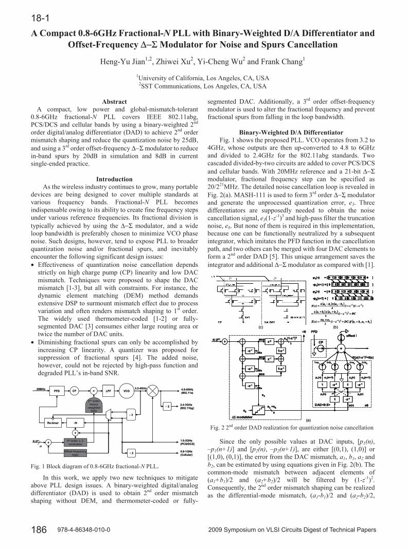
186 978-4-86348-010-0 2009 Symposium on VLSI Circuits Digest of Technical Papers 18-1 A Compact 0.8-6GHz Fractional-N PLL with Binary-Weighted D/A Differentiator and Offset-Frequency ∆ − Σ Modulator for Noise and Spurs Cancellation Heng-Yu Jian 1,2 , Zhiwei Xu 2 , Yi-Cheng Wu 2 and Frank Chang 1 1 University of California, Los Angeles, CA, USA 2 SST Communications, Los Angeles, CA, USA Abstract A compact, low power and global-mismatch-tolerant 0.8-6GHz fractional-N PLL covers IEEE 802.11abg, PCS/DCS and cellular bands by using a binary-weighted 2 nd order digital/analog differentiator (DAD) to achieve 2 nd order mismatch shaping and reduce the quantization noise by 25dB, and using a 3 rd order offset-frequency ∆−Σ modulator to reduce in-band spurs by 20dB in simulation and 8dB in current single-ended practice. Introduction As the wireless industry continues to grow, many portable devices are being designed to cover multiple standards at various frequency bands. Fractional-N PLL becomes indispensable owing to its ability to create fine frequency steps under various reference frequencies. Its fractional division is typically achieved by using the ∆−Σ modulator, and a wide loop bandwidth is preferably chosen to minimize VCO phase noise. Such designs, however, tend to expose PLL to broader quantization noise and/or fractional spurs, and inevitably encounter the following significant design issues: • Effectiveness of quantization noise cancellation depends strictly on high charge pump (CP) linearity and low DAC mismatch. Techniques were proposed to shape the DAC mismatch [1-3], but all with constraints. For instance, the dynamic element matching (DEM) method demands extensive DSP to surmount mismatch effect due to process variation and often renders mismatch shaping to 1 st order. The widely used thermometer-coded [1-2] or fully- segmented DAC [3] consumes either large routing area or twice the number of DAC units. • Diminishing fractional spurs can only be accomplished by increasing CP linearity. A quantizer was proposed for suppression of fractional spurs [4]. The added noise, however, could not be rejected by high-pass function and degraded PLL’s in-band SNR. In this work, we apply two new techniques to mitigate above PLL design issues. A binary-weighted digital/analog differentiator (DAD) is used to obtain 2 nd order mismatch shaping without DEM, and thermometer-coded or fully- segmented DAC. Additionally, a 3 rd order offset-frequency modulator is used to alter the fractional frequency and prevent fractional spurs from falling in the loop bandwidth. Binary-Weighted D/A Differentiator Fig. 1 shows the proposed PLL. VCO operates from 3.2 to 4GHz, whose outputs are then up-converted to 4.8 to 6GHz and divided to 2.4GHz for the 802.11abg standards. Two cascaded divided-by-two circuits are added to cover PCS/DCS and cellular bands. With 20MHz reference and a 21-bit ∆−Σ modulator, fractional frequency step can be specified as 20/2 21 MHz. The detailed noise cancellation loop is revealed in Fig. 2(a). MASH-111 is used to form 3 rd order ∆−Σ ҏ modulator and generate the unprocessed quantization error, e 3 . Three differentiators are supposedly needed to obtain the noise cancellation signal, e 3 (1-z -1 ) 3 and high-pass filter the truncation noise, e 6 . But none of them is required in this implementation, because one can be functionally neutralized by a subsequent integrator, which imitates the PFD function in the cancellation path, and two others can be merged with four DAC elements to form a 2 nd order DAD [5]. This unique arrangement saves the integrator and additional ∆−Σ modulator as compared with [1]. Since the only possible values at DAC inputs, [p 1 (n), –p 1 (n+1)] and [p 2 (n), –p 2 (n+1)], are either [(0,1), (1,0)] or [(1,0), (0,1)], the error from the DAC mismatch, a 1 , b 1 , a 2 and b 2 , can be estimated by using equations given in Fig. 2(b). The common-mode mismatch between adjacent elements of (a 1 +b 1 )/2 and (a 2 +b 2 )/2 will be filtered by (1-z -1 ) 2 . Consequently, the 2 nd order mismatch shaping can be realized as the differential-mode mismatch, (a 1 -b 1 )/2 and (a 2 -b 2 )/2, 4.8-6GHz (802.11a) 2.4-3GHz (802.11bg) 0.8-1GHz (Cellular) 1.6-2GHz (PCS/DCS) 20MHz VCO Ί N LPF PFD CP + Ί 2 Ί 2 Ί 2 21 3.2-4GHz 2 nd order binary -weighted DAD Re-timer + + K·2 21 4.8-6GHz (802.11a) 2.4-3GHz (802.11bg) 0.8-1GHz (Cellular) 1.6-2GHz (PCS/DCS) 20MHz VCO 3 rd order ∆ − Σ modulator Ί N LPF PFD CP + Ί 2 Ί 2 Ί 2 21 3.2-4GHz 2 nd order binary -weighted DAD Re-timer + Offset frequency logic + K·2 21 Fig. 1 Block diagram of 0.8-6GHz fractional-N PLL. K·2 21 6 e 3 (1-z -1 ) 3 e 3 e 6 e 3 +e 6 + offset I 3 CP -z -1 1 -z -1 1 -z -1 1 x6 DAD<0:5> ∆ Σ modulator -z -1 -z -1 -z -1 1-z -1 1-z -1 z -1 z -2 MSB MSB MSB + LSBs LSBs LSBs p1(n) -p1(n+1) p2(n) -p2(n+1) p1(n) p2(n) 1+a 1 1+b 1 1+a 2 1+b 2 PFD Ί N p(n) P(z)(1-z -1 ) 2 +E(z) K·2 21 6 e 3 (1-z -1 ) 3 e 3 e 6 e 3 +e 6 + offset I 3 CP -z -1 1 -z -1 1 -z -1 1 x6 DAD<0:5> ∆ Σ modulator -z -1 -z -1 -z -1 1-z -1 1-z -1 z -1 z -2 MSB MSB MSB + LSBs LSBs LSBs p1(n) -p1(n+1) p2(n) -p2(n+1) p1(n) p2(n) 1+a 1 1+b 1 1+a 2 1+b 2 PFD Ί N p(n) P(z)(1-z -1 ) 2 +E(z) p 1 (n) = [ 0 1 0 1 0 1 0 1 0 1 1 0 0 ] -p 1 (n+1 ) = [ 0 1 0 1 0 1 0 1 0 1 0 0 1 ] p 2 (n) = [ 0 1 0 0 1 1 0 1 0 0 1 1 0 ] -p 2 (n+1) = [ 1 0 1 1 0 0 1 0 1 1 0 0 1 ] ( ) ( ) ( ) ( ) DC z b a b a z z b a b a z E + − + ± + ± + − + − ± − ± = − − − 2 1 2 2 1 1 1 1 2 2 1 1 ) 1 ( 4 ) 1 )( 1 ( 4 ) ( { } 2 2 1 1 2 1 2 1 , ; ) 1 ( 2 ) ( b a b a if DC z a a z E = = + − ± ± = − p 1 (n) = [ 0 1 0 1 0 1 0 1 0 1 1 0 0 ] -p 1 (n+1 ) = [ 0 1 0 1 0 1 0 1 0 1 0 0 1 ] p 2 (n) = [ 0 1 0 0 1 1 0 1 0 0 1 1 0 ] -p 2 (n+1) = [ 1 0 1 1 0 0 1 0 1 1 0 0 1 ] p 1 (n) = [ 0 1 0 1 0 1 0 1 0 1 1 0 0 ] -p 1 (n+1 ) = [ 0 1 0 1 0 1 0 1 0 1 0 0 1 ] p 2 (n) = [ 0 1 0 0 1 1 0 1 0 0 1 1 0 ] -p 2 (n+1) = [ 1 0 1 1 0 0 1 0 1 1 0 0 1 ] ( ) ( ) ( ) ( ) DC z b a b a z z b a b a z E + − + ± + ± + − + − ± − ± = − − − 2 1 2 2 1 1 1 1 2 2 1 1 ) 1 ( 4 ) 1 )( 1 ( 4 ) ( { } 2 2 1 1 2 1 2 1 , ; ) 1 ( 2 ) ( b a b a if DC z a a z E = = + − ± ± = − (a) (c) (b) K·2 21 6 e 3 (1-z -1 ) 3 e 3 e 6 e 3 +e 6 + offset I 3 CP -z -1 1 -z -1 1 -z -1 1 x6 DAD<0:5> ∆ Σ modulator -z -1 -z -1 -z -1 1-z -1 1-z -1 z -1 z -2 MSB MSB MSB + LSBs LSBs LSBs p1(n) -p1(n+1) p2(n) -p2(n+1) p1(n) p2(n) 1+a 1 1+b 1 1+a 2 1+b 2 PFD Ί N p(n) P(z)(1-z -1 ) 2 +E(z) K·2 21 6 e 3 (1-z -1 ) 3 e 3 e 6 e 3 +e 6 + offset I 3 CP -z -1 1 -z -1 1 -z -1 1 x6 DAD<0:5> ∆ Σ modulator -z -1 -z -1 -z -1 1-z -1 1-z -1 z -1 z -2 MSB MSB MSB + LSBs LSBs LSBs p1(n) -p1(n+1) p2(n) -p2(n+1) p1(n) p2(n) 1+a 1 1+b 1 1+a 2 1+b 2 PFD Ί N p(n) P(z)(1-z -1 ) 2 +E(z) p 1 (n) = [ 0 1 0 1 0 1 0 1 0 1 1 0 0 ] -p 1 (n+1 ) = [ 0 1 0 1 0 1 0 1 0 1 0 0 1 ] p 2 (n) = [ 0 1 0 0 1 1 0 1 0 0 1 1 0 ] -p 2 (n+1) = [ 1 0 1 1 0 0 1 0 1 1 0 0 1 ] ( ) ( ) ( ) ( ) DC z b a b a z z b a b a z E + − + ± + ± + − + − ± − ± = − − − 2 1 2 2 1 1 1 1 2 2 1 1 ) 1 ( 4 ) 1 )( 1 ( 4 ) ( { } 2 2 1 1 2 1 2 1 , ; ) 1 ( 2 ) ( b a b a if DC z a a z E = = + − ± ± = − p 1 (n) = [ 0 1 0 1 0 1 0 1 0 1 1 0 0 ] -p 1 (n+1 ) = [ 0 1 0 1 0 1 0 1 0 1 0 0 1 ] p 2 (n) = [ 0 1 0 0 1 1 0 1 0 0 1 1 0 ] -p 2 (n+1) = [ 1 0 1 1 0 0 1 0 1 1 0 0 1 ] p 1 (n) = [ 0 1 0 1 0 1 0 1 0 1 1 0 0 ] -p 1 (n+1 ) = [ 0 1 0 1 0 1 0 1 0 1 0 0 1 ] p 2 (n) = [ 0 1 0 0 1 1 0 1 0 0 1 1 0 ] -p 2 (n+1) = [ 1 0 1 1 0 0 1 0 1 1 0 0 1 ] ( ) ( ) ( ) ( ) DC z b a b a z z b a b a z E + − + ± + ± + − + − ± − ± = − − − 2 1 2 2 1 1 1 1 2 2 1 1 ) 1 ( 4 ) 1 )( 1 ( 4 ) ( { } 2 2 1 1 2 1 2 1 , ; ) 1 ( 2 ) ( b a b a if DC z a a z E = = + − ± ± = − (a) (c) (b) Fig. 2 2 nd order DAD realization for quantization noise cancellation
Transcript of 18-1 A Compact 0.8-6GHz Fractional-N PLL with Binary...
186 978-4-86348-010-0 2009 Symposium on VLSI Circuits Digest of Technical Papers
18-1A Compact 0.8-6GHz Fractional-N PLL with Binary-Weighted D/A Differentiator and
Offset-Frequency ∆−Σ Modulator for Noise and Spurs Cancellation
Heng-Yu Jian1,2, Zhiwei Xu2, Yi-Cheng Wu2 and Frank Chang1
1University of California, Los Angeles, CA, USA
2SST Communications, Los Angeles, CA, USA
Abstract
A compact, low power and global-mismatch-tolerant 0.8-6GHz fractional-N PLL covers IEEE 802.11abg, PCS/DCS and cellular bands by using a binary-weighted 2nd order digital/analog differentiator (DAD) to achieve 2nd order mismatch shaping and reduce the quantization noise by 25dB, and using a 3rd order offset-frequency ∆−Σ modulator to reduce in-band spurs by 20dB in simulation and 8dB in current single-ended practice.
Introduction
As the wireless industry continues to grow, many portable devices are being designed to cover multiple standards at various frequency bands. Fractional-N PLL becomes indispensable owing to its ability to create fine frequency steps under various reference frequencies. Its fractional division is typically achieved by using the ∆−Σ modulator, and a wide loop bandwidth is preferably chosen to minimize VCO phase noise. Such designs, however, tend to expose PLL to broader quantization noise and/or fractional spurs, and inevitably encounter the following significant design issues: • Effectiveness of quantization noise cancellation depends
strictly on high charge pump (CP) linearity and low DAC mismatch. Techniques were proposed to shape the DAC mismatch [1-3], but all with constraints. For instance, the dynamic element matching (DEM) method demands extensive DSP to surmount mismatch effect due to process variation and often renders mismatch shaping to 1st order. The widely used thermometer-coded [1-2] or fully- segmented DAC [3] consumes either large routing area or twice the number of DAC units.
• Diminishing fractional spurs can only be accomplished by increasing CP linearity. A quantizer was proposed for suppression of fractional spurs [4]. The added noise, however, could not be rejected by high-pass function and degraded PLL’s in-band SNR.
In this work, we apply two new techniques to mitigate above PLL design issues. A binary-weighted digital/analog differentiator (DAD) is used to obtain 2nd order mismatch shaping without DEM, and thermometer-coded or fully-
segmented DAC. Additionally, a 3rd order offset-frequency modulator is used to alter the fractional frequency and prevent fractional spurs from falling in the loop bandwidth.
Binary-Weighted D/A Differentiator
Fig. 1 shows the proposed PLL. VCO operates from 3.2 to 4GHz, whose outputs are then up-converted to 4.8 to 6GHz and divided to 2.4GHz for the 802.11abg standards. Two cascaded divided-by-two circuits are added to cover PCS/DCS and cellular bands. With 20MHz reference and a 21-bit ∆−Σ modulator, fractional frequency step can be specified as 20/221MHz. The detailed noise cancellation loop is revealed in Fig. 2(a). MASH-111 is used to form 3rd order ∆−Σ modulator and generate the unprocessed quantization error, e3. Three differentiators are supposedly needed to obtain the noise cancellation signal, e3(1-z-1)3 and high-pass filter the truncation noise, e6. But none of them is required in this implementation, because one can be functionally neutralized by a subsequent integrator, which imitates the PFD function in the cancellation path, and two others can be merged with four DAC elements to form a 2nd order DAD [5]. This unique arrangement saves the integrator and additional ∆−Σ modulator as compared with [1].
Since the only possible values at DAC inputs, [p1(n), –p1(n+1)] and [p2(n), –p2(n+1)], are either [(0,1), (1,0)] or [(1,0), (0,1)], the error from the DAC mismatch, a1, b1, a2 and b2, can be estimated by using equations given in Fig. 2(b). The common-mode mismatch between adjacent elements of (a1+b1)/2 and (a2+b2)/2 will be filtered by (1-z-1)2. Consequently, the 2nd order mismatch shaping can be realized as the differential-mode mismatch, (a1-b1)/2 and (a2-b2)/2,
4.8-6GHz(802.11a)
2.4-3GHz(802.11bg)
0.8-1GHz(Cellular)
1.6-2GHz(PCS/DCS)
20MHzVCO
3rd order ∆−Σ modulator
N
LPFPFD CP +
2
2
2
21
3.2-4GHz
2nd orderbinary
-weightedDAD
Re-timer
+
Offset frequencylogic
+
K·221
4.8-6GHz(802.11a)
2.4-3GHz(802.11bg)
0.8-1GHz(Cellular)
1.6-2GHz(PCS/DCS)
20MHzVCO
3rd order ∆−Σ modulator
N
LPFPFD CP +
2
2
2
21
3.2-4GHz
2nd orderbinary
-weightedDAD
Re-timer
+
Offset frequencylogic
+
K·221
Fig. 1 Block diagram of 0.8-6GHz fractional-N PLL.
K·221
6
e3(1-z-1)3
e3
e6
e3 +e6
+
offset I
3 CP
-z-11 -z-11
-z-11
x6DAD<0:5>
∆Σ modulator
-z-1
-z-1
-z-1
1-z-1
1-z-1
z-1
z-2MSB
MSB
MSB
+
LSBs
LSBs
LSBs
p1(n) -p1(n+1) p2(n) -p2(n+1)
p1(n) p2(n)
1+a1 1+b1 1+a2 1+b2
PFDN
p(n)
P(z)(1-z-1)2+E(z)
K·221
6
e3(1-z-1)3
e3
e6
e3 +e6
+
offset I
3 CP
-z-11 -z-11
-z-11
x6DAD<0:5>
∆Σ modulator
-z-1
-z-1
-z-1
1-z-1
1-z-1
z-1
z-2MSB
MSB
MSB
+
LSBs
LSBs
LSBs
p1(n) -p1(n+1) p2(n) -p2(n+1)
p1(n) p2(n)
1+a1 1+b1 1+a2 1+b2
PFDN
p(n)
P(z)(1-z-1)2+E(z)
p1(n) = [ 0 1 0 1 0 1 0 1 0 1 1 0 0 ]
-p1(n+1) = [ 0 1 0 1 0 1 0 1 0 1 0 0 1 ]
p2(n) = [ 0 1 0 0 1 1 0 1 0 0 1 1 0 ]
-p2(n+1) = [ 1 0 1 1 0 0 1 0 1 1 0 0 1 ]
( ) ( )
( ) ( ) DCzbaba
zzbabazE
+−+±+±+
−+−±−±=
−
−−
212211
112211
)1(4
)1)(1(4
)(
{ }22112121 ,;)1(
2)( babaifDCzaazE ==+−±±= −
p1(n) = [ 0 1 0 1 0 1 0 1 0 1 1 0 0 ]
-p1(n+1) = [ 0 1 0 1 0 1 0 1 0 1 0 0 1 ]
p2(n) = [ 0 1 0 0 1 1 0 1 0 0 1 1 0 ]
-p2(n+1) = [ 1 0 1 1 0 0 1 0 1 1 0 0 1 ]
p1(n) = [ 0 1 0 1 0 1 0 1 0 1 1 0 0 ]
-p1(n+1) = [ 0 1 0 1 0 1 0 1 0 1 0 0 1 ]
p2(n) = [ 0 1 0 0 1 1 0 1 0 0 1 1 0 ]
-p2(n+1) = [ 1 0 1 1 0 0 1 0 1 1 0 0 1 ]
( ) ( )
( ) ( ) DCzbaba
zzbabazE
+−+±+±+
−+−±−±=
−
−−
212211
112211
)1(4
)1)(1(4
)(
{ }22112121 ,;)1(
2)( babaifDCzaazE ==+−±±= −
(a)
(c) (b)
K·221
6
e3(1-z-1)3
e3
e6
e3 +e6
+
offset I
3 CP
-z-11 -z-11
-z-11
x6DAD<0:5>
∆Σ modulator
-z-1
-z-1
-z-1
1-z-1
1-z-1
z-1
z-2MSB
MSB
MSB
+
LSBs
LSBs
LSBs
p1(n) -p1(n+1) p2(n) -p2(n+1)
p1(n) p2(n)
1+a1 1+b1 1+a2 1+b2
PFDN
p(n)
P(z)(1-z-1)2+E(z)
K·221
6
e3(1-z-1)3
e3
e6
e3 +e6
+
offset I
3 CP
-z-11 -z-11
-z-11
x6DAD<0:5>
∆Σ modulator
-z-1
-z-1
-z-1
1-z-1
1-z-1
z-1
z-2MSB
MSB
MSB
+
LSBs
LSBs
LSBs
p1(n) -p1(n+1) p2(n) -p2(n+1)
p1(n) p2(n)
1+a1 1+b1 1+a2 1+b2
PFDN
p(n)
P(z)(1-z-1)2+E(z)
p1(n) = [ 0 1 0 1 0 1 0 1 0 1 1 0 0 ]
-p1(n+1) = [ 0 1 0 1 0 1 0 1 0 1 0 0 1 ]
p2(n) = [ 0 1 0 0 1 1 0 1 0 0 1 1 0 ]
-p2(n+1) = [ 1 0 1 1 0 0 1 0 1 1 0 0 1 ]
( ) ( )
( ) ( ) DCzbaba
zzbabazE
+−+±+±+
−+−±−±=
−
−−
212211
112211
)1(4
)1)(1(4
)(
{ }22112121 ,;)1(
2)( babaifDCzaazE ==+−±±= −
p1(n) = [ 0 1 0 1 0 1 0 1 0 1 1 0 0 ]
-p1(n+1) = [ 0 1 0 1 0 1 0 1 0 1 0 0 1 ]
p2(n) = [ 0 1 0 0 1 1 0 1 0 0 1 1 0 ]
-p2(n+1) = [ 1 0 1 1 0 0 1 0 1 1 0 0 1 ]
p1(n) = [ 0 1 0 1 0 1 0 1 0 1 1 0 0 ]
-p1(n+1) = [ 0 1 0 1 0 1 0 1 0 1 0 0 1 ]
p2(n) = [ 0 1 0 0 1 1 0 1 0 0 1 1 0 ]
-p2(n+1) = [ 1 0 1 1 0 0 1 0 1 1 0 0 1 ]
( ) ( )
( ) ( ) DCzbaba
zzbabazE
+−+±+±+
−+−±−±=
−
−−
212211
112211
)1(4
)1)(1(4
)(
{ }22112121 ,;)1(
2)( babaifDCzaazE ==+−±±= −
(a)
(c) (b)
Fig. 2 2nd order DAD realization for quantization noise cancellation
1872009 Symposium on VLSI Circuits Digest of Technical Papers
between adjacent elements is minimized. The DAC matching requirement can therefore be relaxed to only local matching between adjacent DAC pairs, which are easy to route symmetrically with interdigitated technique without using complicated selection mechanism of prior arts to reduce global mismatches. The multi-bit DAD can also be implemented with binary-weighted architecture because gain error in each binary-weighted element can be treated as the common-mode mismatch and will be filtered by 2nd order high-pass function. Compared with the thermometer-coded (or fully-segmented) DAC with 1st order DEM, the 2nd-order binary-weighted DAD offers 20dB more mismatch reduction in simulation [5] and occupies smaller chip area. Additionally, an offset current pulse is added to enhance the CP linearity and compensate for unsigned DAD operation. The matching between CP and DAD can be attained with the same NMOS to replicate each other as shown in Fig. 2(c).
Offset-Frequency ∆−Σ Modulator
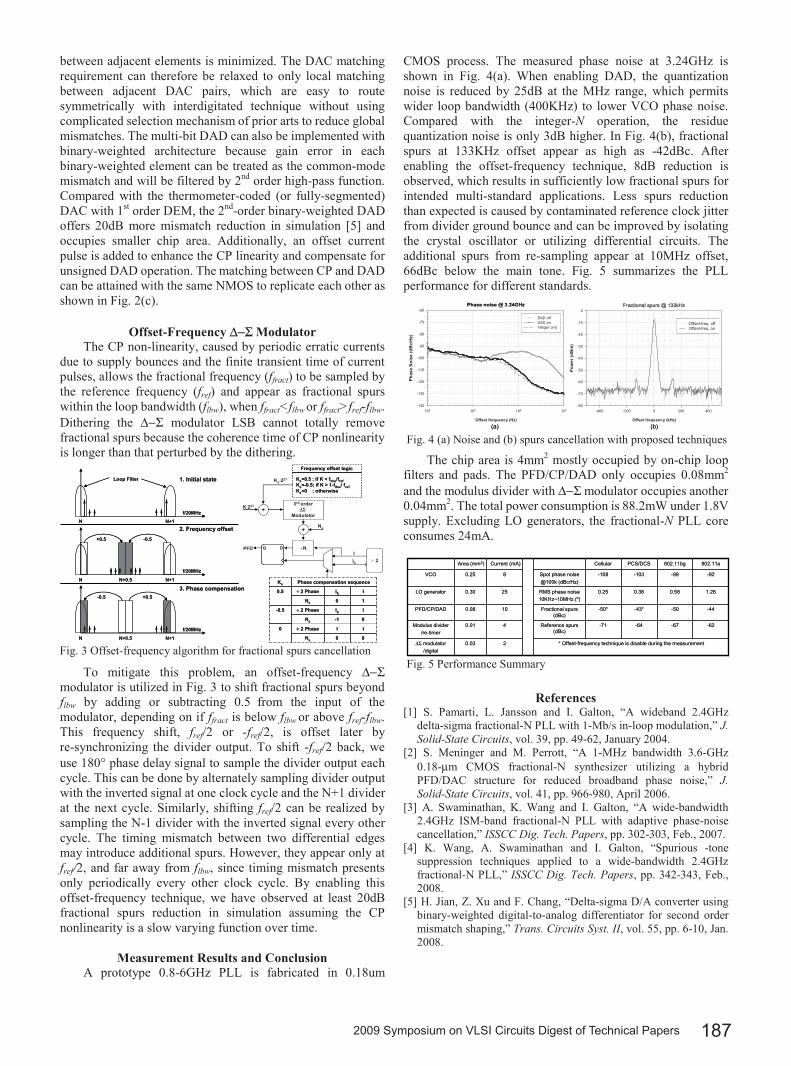
The CP non-linearity, caused by periodic erratic currents due to supply bounces and the finite transient time of current pulses, allows the fractional frequency (ffract) to be sampled by the reference frequency (fref) and appear as fractional spurs within the loop bandwidth (flbw), when ffract<flbw or ffract>fref-flbw. Dithering the ∆−Σ modulator LSB cannot totally remove fractional spurs because the coherence time of CP nonlinearity is longer than that perturbed by the dithering.
To mitigate this problem, an offset-frequency ∆−Σ modulator is utilized in Fig. 3 to shift fractional spurs beyond flbw by adding or subtracting 0.5 from the input of the modulator, depending on if ffract is below flbw or above fref-flbw. This frequency shift, fref/2 or -fref/2, is offset later by re-synchronizing the divider output. To shift -fref/2 back, we use 180° phase delay signal to sample the divider output each cycle. This can be done by alternately sampling divider output with the inverted signal at one clock cycle and the N+1 divider at the next cycle. Similarly, shifting fref/2 can be realized by sampling the N-1 divider with the inverted signal every other cycle. The timing mismatch between two differential edges may introduce additional spurs. However, they appear only at fref/2, and far away from flbw, since timing mismatch presents only periodically every other clock cycle. By enabling this offset-frequency technique, we have observed at least 20dB fractional spurs reduction in simulation assuming the CP nonlinearity is a slow varying function over time.
Measurement Results and Conclusion A prototype 0.8-6GHz PLL is fabricated in 0.18um
CMOS process. The measured phase noise at 3.24GHz is shown in Fig. 4(a). When enabling DAD, the quantization noise is reduced by 25dB at the MHz range, which permits wider loop bandwidth (400KHz) to lower VCO phase noise. Compared with the integer-N operation, the residue quantization noise is only 3dB higher. In Fig. 4(b), fractional spurs at 133KHz offset appear as high as -42dBc. After enabling the offset-frequency technique, 8dB reduction is observed, which results in sufficiently low fractional spurs for intended multi-standard applications. Less spurs reduction than expected is caused by contaminated reference clock jitter from divider ground bounce and can be improved by isolating the crystal oscillator or utilizing differential circuits. The additional spurs from re-sampling appear at 10MHz offset, 66dBc below the main tone. Fig. 5 summarizes the PLL performance for different standards.
The chip area is 4mm2 mostly occupied by on-chip loop filters and pads. The PFD/CP/DAD only occupies 0.08mm2 and the modulus divider with ∆−Σ modulator occupies another 0.04mm2. The total power consumption is 88.2mW under 1.8V supply. Excluding LO generators, the fractional-N PLL core consumes 24mA.
References
[1] S. Pamarti, L. Jansson and I. Galton, “A wideband 2.4GHz delta-sigma fractional-N PLL with 1-Mb/s in-loop modulation,” J. Solid-State Circuits, vol. 39, pp. 49-62, January 2004.
[2] S. Meninger and M. Perrott, “A 1-MHz bandwidth 3.6-GHz 0.18-µm CMOS fractional-N synthesizer utilizing a hybrid PFD/DAC structure for reduced broadband phase noise,” J. Solid-State Circuits, vol. 41, pp. 966-980, April 2006.
[3] A. Swaminathan, K. Wang and I. Galton, “A wide-bandwidth 2.4GHz ISM-band fractional-N PLL with adaptive phase-noise cancellation,” ISSCC Dig. Tech. Papers, pp. 302-303, Feb., 2007.
[4] K. Wang, A. Swaminathan and I. Galton, “Spurious -tone suppression techniques applied to a wide-bandwidth 2.4GHz fractional-N PLL,” ISSCC Dig. Tech. Papers, pp. 342-343, Feb., 2008.
[5] H. Jian, Z. Xu and F. Chang, “Delta-sigma D/A converter using binary-weighted digital-to-analog differentiator for second order mismatch shaping,” Trans. Circuits Syst. II, vol. 55, pp. 6-10, Jan. 2008.
Frequency (Hz)
104 105 106 107Ph
ase
Noi
se (d
Bc/
Hz)
-140
-130
-120
-110
-100
-90
-80
-70
-60
DAD off DAD on Integer only
Phase noise @ 3.24GHz
Offset frequency (KHz)
-400 -200 0 200 400
Pow
er (d
Bm
)
-80
-70
-60
-50
-40
-30
-20
-10
0
Cancellation offCancellation on
Offset frequency (kHz)Offset frequency (Hz)
Offset-freq. offOffset-freq. on
(a) (b)Frequency (Hz)
104 105 106 107Ph
ase
Noi
se (d
Bc/
Hz)
-140
-130
-120
-110
-100
-90
-80
-70
-60
DAD off DAD on Integer only
Phase noise @ 3.24GHz
Offset frequency (KHz)
-400 -200 0 200 400
Pow
er (d
Bm
)
-80
-70
-60
-50
-40
-30
-20
-10
0
Cancellation offCancellation on
Offset frequency (kHz)Offset frequency (Hz)
Offset-freq. offOffset-freq. on
(a) (b)
Fig. 4 (a) Noise and (b) spurs cancellation with proposed techniques
-62
-44
1.28
-92
802.11a
2
4
10
25
8
Current (mA)
* Offset-frequency technique is disable during the measurement
Reference spurs (dBc)
Fractional spurs (dBc)
RMS phase noise10KHz~10MHz (º)
Spot phase noise @100k (dBc/Hz)
-71
-50*
0.25
-108
Cellular
-64
-43*
0.38
-103
PCS/DCS
0.03∆Σ modulator/digital
-670.01Modulus divider/re-timer
-500.08PFD/CP/DAD
0.580.30LO generator
-990.25VCO
802.11bgArea (mm2)
Fig. 5 Performance Summary
0-1Ns
IIb2 Phase-0.5
10Ns
IIb2 Phase0.5
0
Ks
0
I
Phase compensation sequence
0Ns
I2 Phase
0-1Ns
IIb2 Phase-0.5
10Ns
IIb2 Phase0.5
0
Ks
0
I
Phase compensation sequence
0Ns
I2 Phase
K·221+
2IIb
3rd order∆Σ
Modulator
+
DQ DQ N
Ks·221
Ns
PFD
Ks=0.5 ; if K < flbw/frefKs=-0.5; if K > 1-flbw/ frefKs=0 ; otherwise
Frequency offset logic
Ks=0.5 ; if K < flbw/frefKs=-0.5; if K > 1-flbw/ frefKs=0 ; otherwise
Frequency offset logic
f/20MHz
N N+1
Loop Filter 1. Initial state
f/20MHz
N N+1
Loop Filter 1. Initial state
f/20MHz
N N+0.5 N+1
-0.5 +0.53. Phase compensation
f/20MHz
N N+0.5 N+1
-0.5 +0.53. Phase compensation
f/20MHz
N N+0.5 N+1
+0.5 -0.5
2. Frequency offset
f/20MHz
N N+0.5 N+1
+0.5 -0.5
2. Frequency offset
Fig. 3 Offset-frequency algorithm for fractional spurs cancellation