Optical Spectroscopies of Thin Films and Interfacesrote/Zahn/Ellipsometry.pdf~ sin2 sin tan - near...
40
Dietrich R. T. Zahn Institut für Physik, Technische Universität Chemnitz, Germany Optical Spectroscopies of Thin Films and Interfaces
Transcript of Optical Spectroscopies of Thin Films and Interfacesrote/Zahn/Ellipsometry.pdf~ sin2 sin tan - near...
Dietrich R. T. ZahnInstitut für Physik, Technische Universität Chemnitz, Germany
Optical Spectroscopies of Thin Films and Interfaces
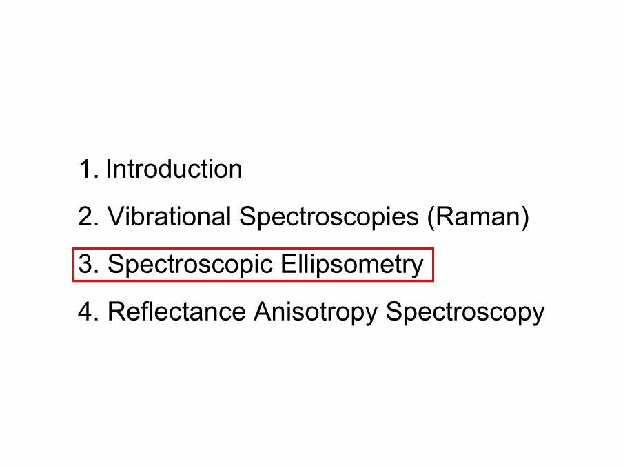
1. Introduction
2. Vibrational Spectroscopies (Raman)
3. Spectroscopic Ellipsometry
4. Reflectance Anisotropy Spectroscopy
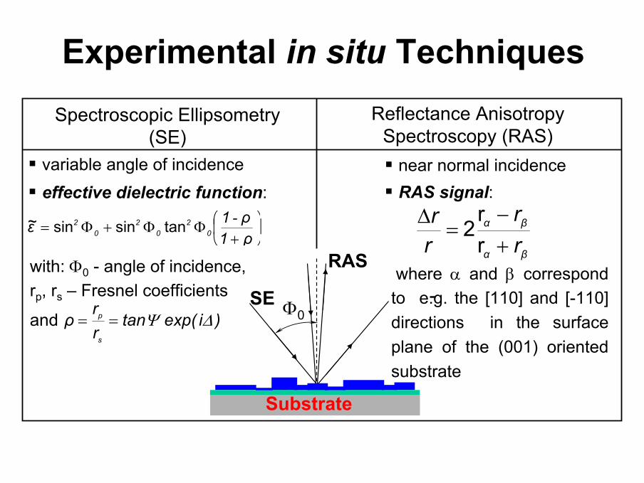
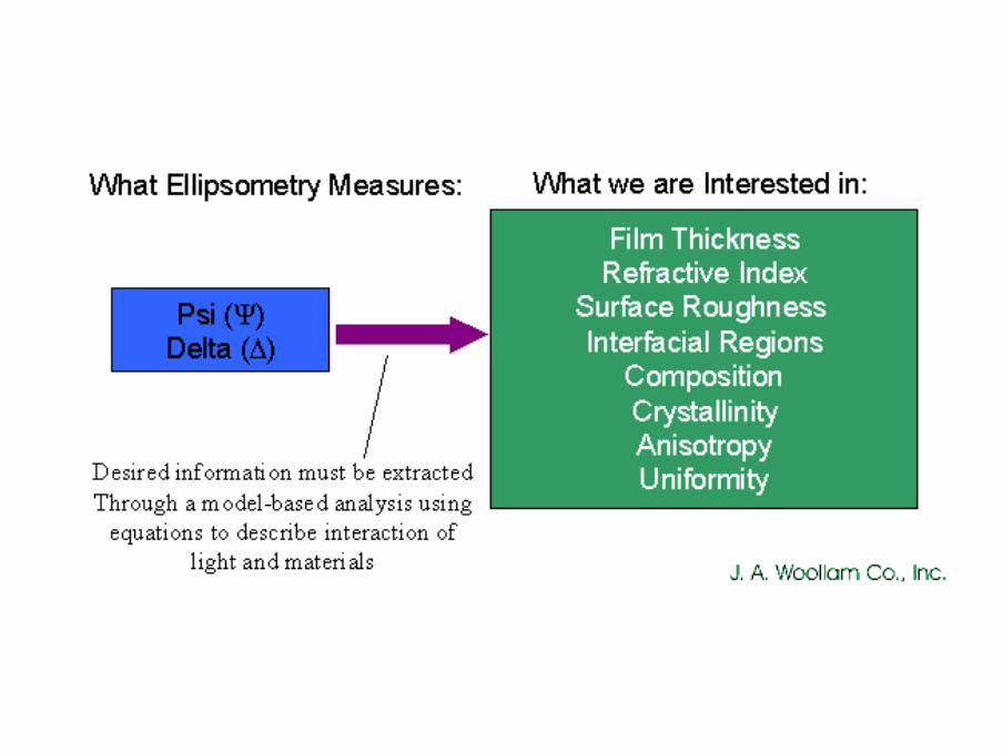
Spectroscopic Ellipsometry(SE)
Reflectance AnisotropySpectroscopy (RAS)
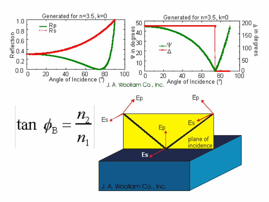
variable angle of incidence
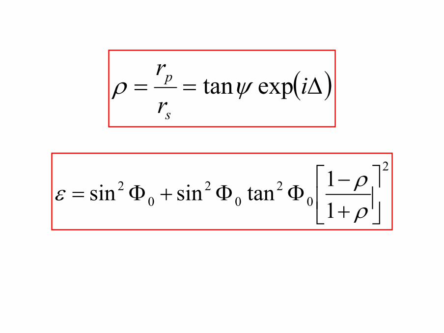
)iexp(tanrr
ρs
p ∆Ψ==
+ΦΦ+Φ=
ρ1ρ1ε 0
20
20
2 -tansinsin~
near normal incidenceRAS signal:effective dielectric function:
with: Φ0 - angle of incidence,rp, rs – Fresnel coefficients
and
βα
βα
rr
rr
+−
=∆
rr
2
where α and β correspond to e.g. the [110] and [-110] directions in the surface plane of the (001) oriented substrate
RAS
SE Φ0
Substrate
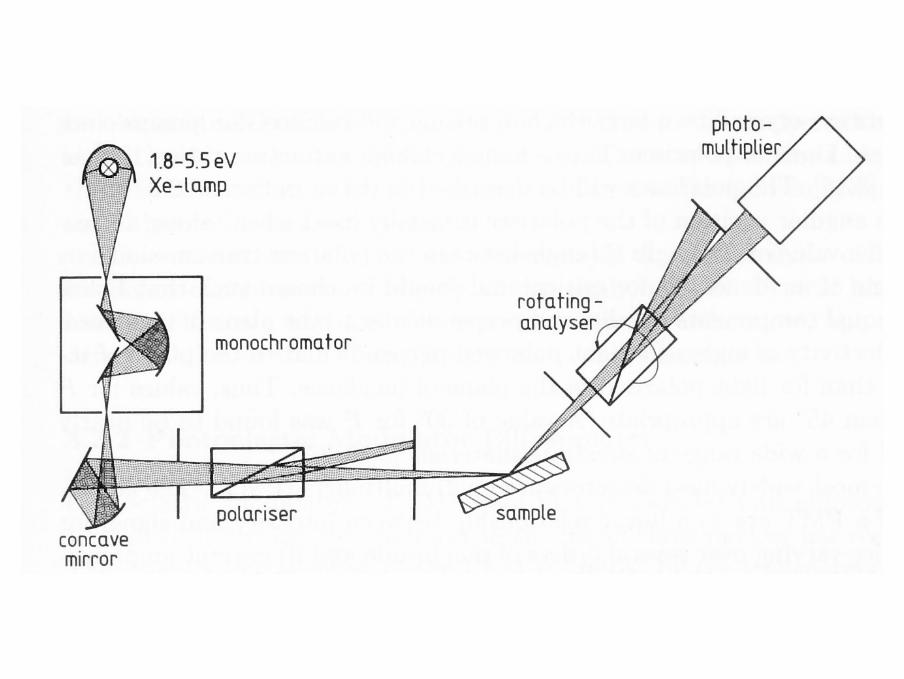
Experimental in situ Techniques
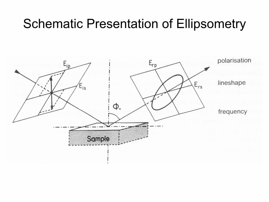
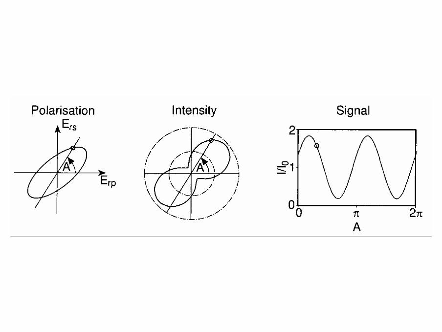
Schematic Presentation of Ellipsometry
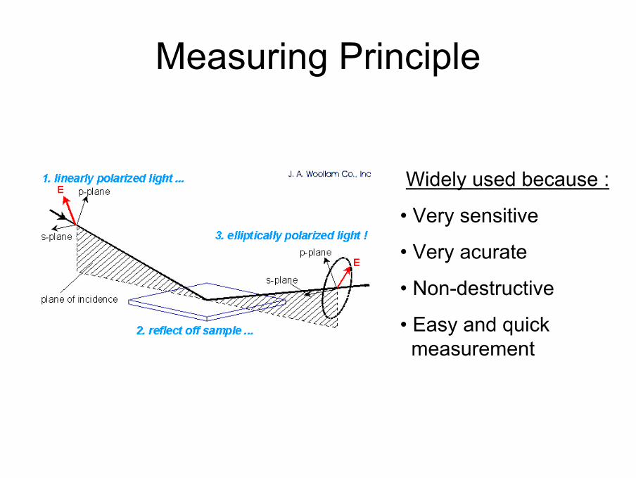
Measuring Principle
Widely used because :
• Very sensitive
• Very acurate
• Non-destructive
• Easy and quick measurement
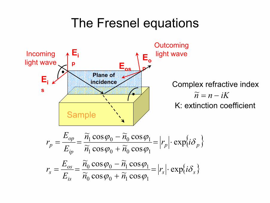
The Fresnel equations
{ }ppip
opp ir
nnnn
EE
r δϕϕϕϕ exp
cos~cos~cos~cos~
1001
1001 ⋅=+−
==
{ }ssis
oss ir
nnnn
EEr δ
ϕϕϕϕ exp
cos~cos~cos~cos~
1100
1100 ⋅=+−
==
iKnn −=~Complex refractive index
K: extinction coefficient
Eip Eos
Eop
Eis
Plane of incidence
Incominglight wave
Outcominglight wave
Sample
2
02
02
02
11tansinsin
+−
ΦΦ+Φ=ρρε
( )∆== irr
s
p exptanψρ
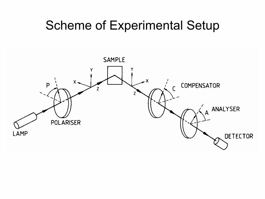
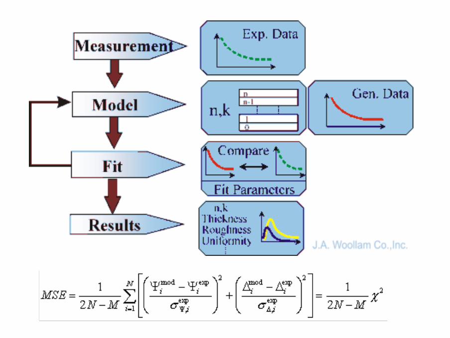
Scheme of Experimental Setup
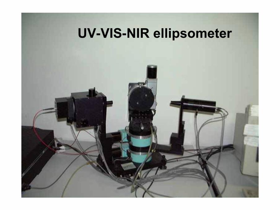
UV-VIS-NIR ellipsometer
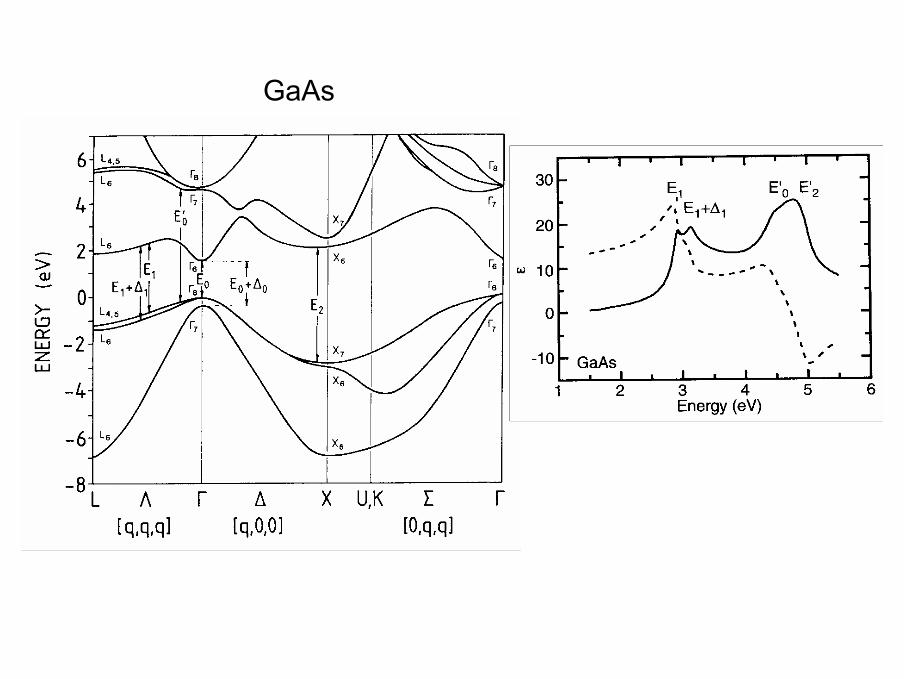
GaAs
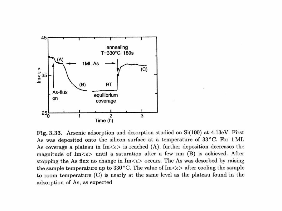
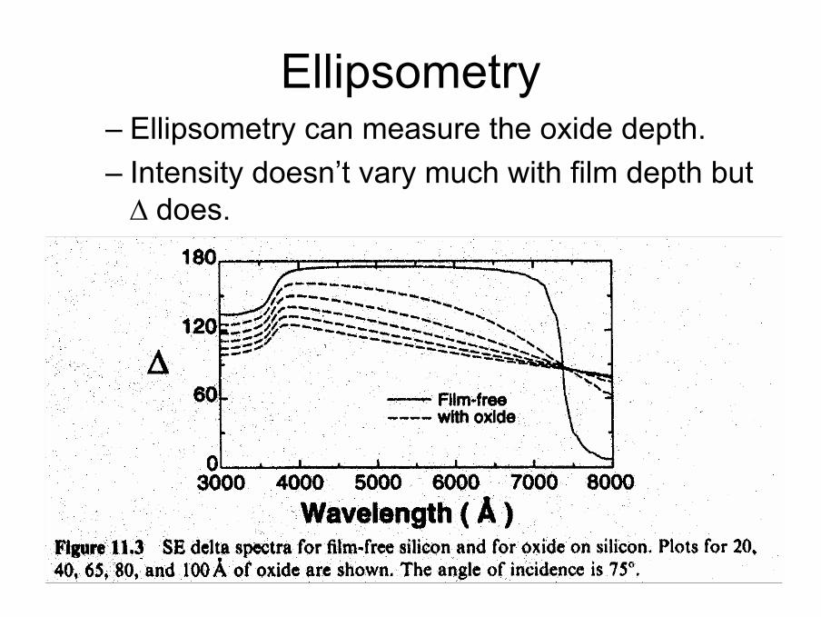
Ellipsometry– Ellipsometry can measure the oxide depth.– Intensity doesn’t vary much with film depth but∆ does.
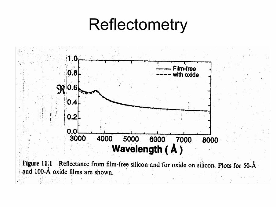
Reflectometry
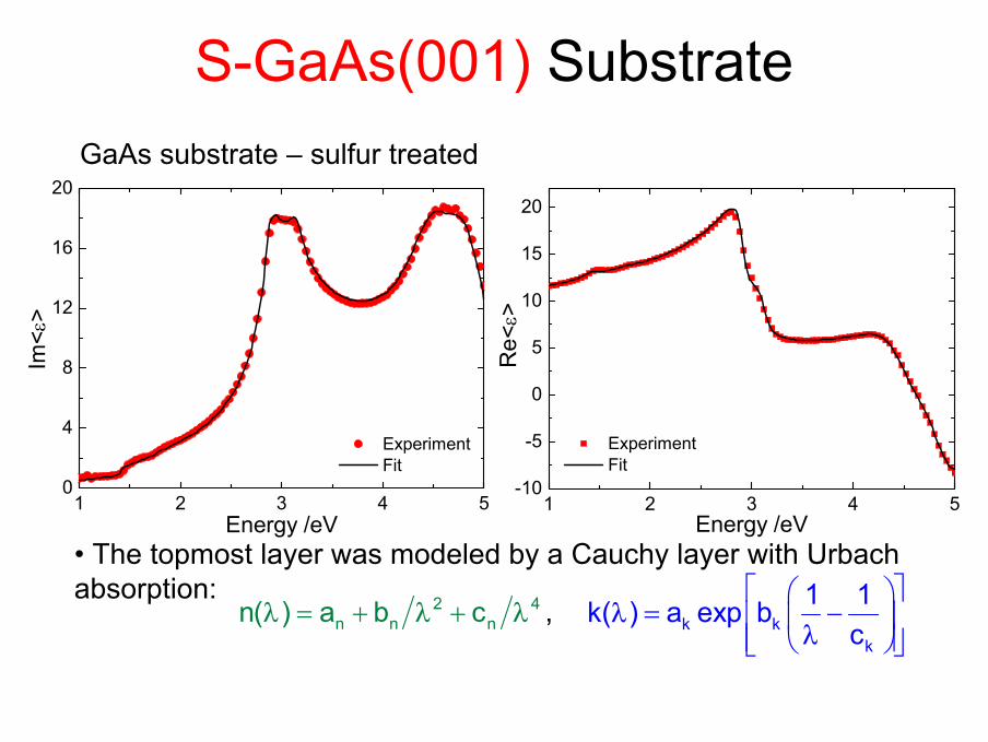
S-GaAs(001) Substrate
1 2 3 4 50
4
8
12
16
20
Experiment Fit
Im<ε
>
Energy /eV1 2 3 4 5
-10
-5
0
5
10
15
20
Experiment Fit
Re<
ε>Energy /eV
GaAs substrate – sulfur treated
• The topmost layer was modeled by a Cauchy layer with Urbachabsorption: 2 4
n n nn( ) a b cλ λ λ= + + k kk
1 1k( ) a exp bc
λλ
= −
,
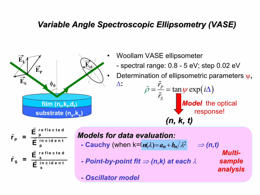
• Woollam VASE ellipsometer- spectral range: 0.8 - 5 eV; step 0.02 eV
• Determination of ellipsometric parameters ψ, ∆:
Variable Angle Variable Angle SpectroscopicSpectroscopic Ellipsometry (VASE)Ellipsometry (VASE)
ES
EP
substrate (ns,ks)film (nf,kf,df)
EL Eel
φ0
%%
%
%%
%
r e f l e c t e dp
P i n c i d e n tp
r e f l e c t e ds
S i n c i d e n ts
Er =
E
Er =E
( )tan expP
S
r ir
ψρ = = ∆%%
%
(n, k, t)(n, k, t)
ModelModel the optical response!
Models for data evaluationModels for data evaluation::- Cauchy (when k=0) ⇒ (n,t)
- Point-by-point fit ⇒ (n,k) at each λ
- Oscillator model
2λλ)( nn ban +=MultiMulti--
sample sample analysisanalysis
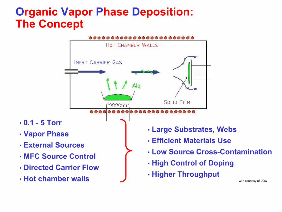
• 0.1 - 5 Torr• Vapor Phase• External Sources• MFC Source Control• Directed Carrier Flow • Hot chamber walls
• Large Substrates, Webs• Efficient Materials Use• Low Source Cross-Contamination• High Control of Doping • Higher Throughput
Organic Vapor Phase Deposition:The Concept
with courtesy of UDC
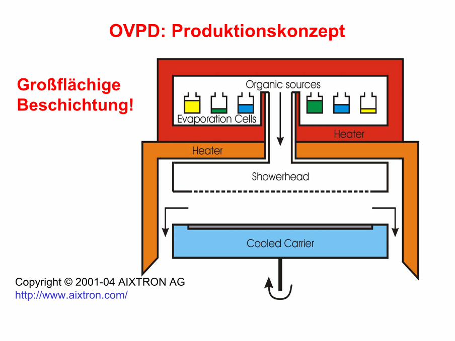
OVPD: Produktionskonzept
Großflächige Beschichtung!
Copyright © 2001-04 AIXTRON AGhttp://www.aixtron.com/
Institut für HochfrequenztechnikTU Braunschweig
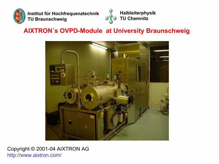
AIXTRON´s OVPD-Module at University Braunschweig
HalbleiterphysikTU Chemnitz
Copyright © 2001-04 AIXTRON AGhttp://www.aixtron.com/
Institut für HochfrequenztechnikTU Braunschweig
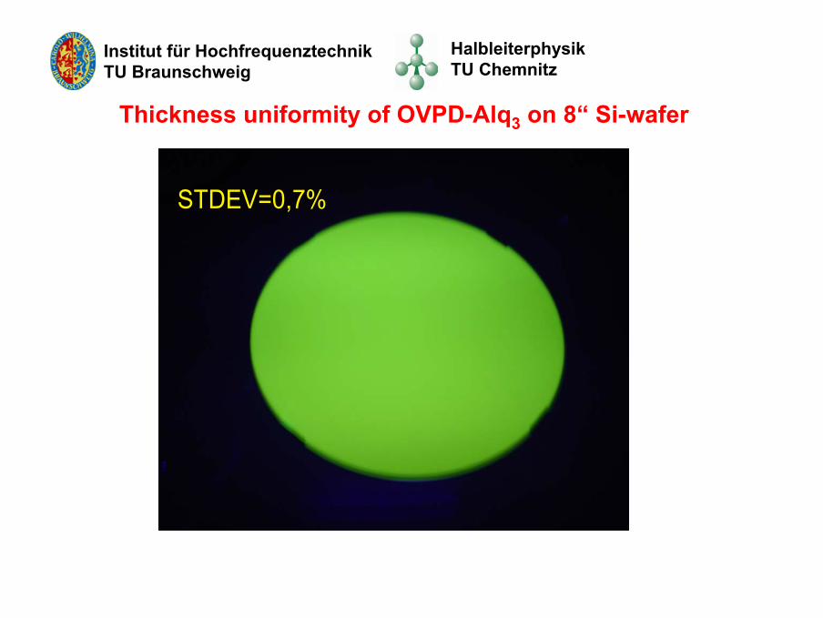
Thickness uniformity of OVPD-Alq3 on 8“ Si-wafer
STDEV=0,7%
HalbleiterphysikTU Chemnitz
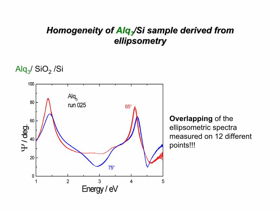
Homogeneity of Homogeneity of AlqAlq33/Si/Si sample derived from sample derived from ellipsometryellipsometry
Overlapping of the ellipsometric spectra measured on 12 different points!!!
Alq3/ SiO2 /Si
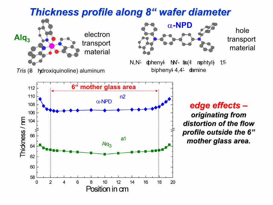
Thickness profile along 8“ wafer diameterThickness profile along 8“ wafer diameter
edge effects edge effects ––originating from originating from
distortion of the flow distortion of the flow profile outside the 6” profile outside the 6”
mother glass area.mother glass area.
6“ mother glass area
Alq3
α-NPD
Tris (8- hydroxiquinoline) aluminumN,N’- diphenyl- N,N’- bis(1- naphtyl)- 1,1’-
biphenyl- 4,4’- diamine
electrontransport material
holetransport material
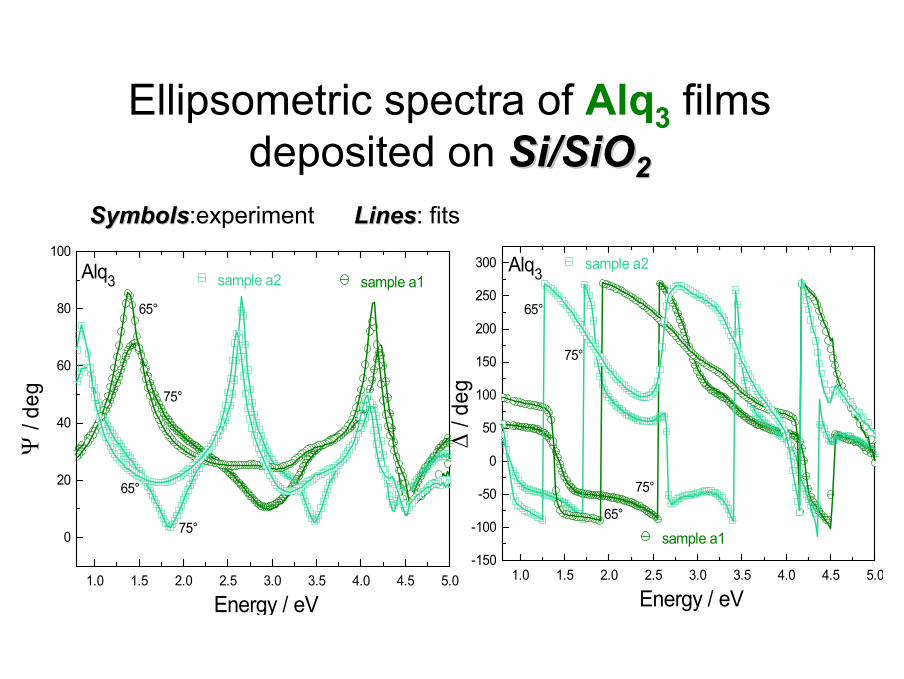
1.0 1.5 2.0 2.5 3.0 3.5 4.0 4.5 5.0
0
20
40
60
80
100
65°
65°
75°
75°
sample a2 sample a1
Energy / eV
Alq3
Ψ /
deg
1.0 1.5 2.0 2.5 3.0 3.5 4.0 4.5 5.0-150
-100
-50
0
50
100
150
200
250
300
65°
65°
75°
75°
sample a2
sample a1
Energy / eV
Alq3
∆ / d
eg
Ellipsometric spectra of Alq3 films deposited on Si/SiOSi/SiO22
SymbolsSymbols:experiment LinesLines: fits
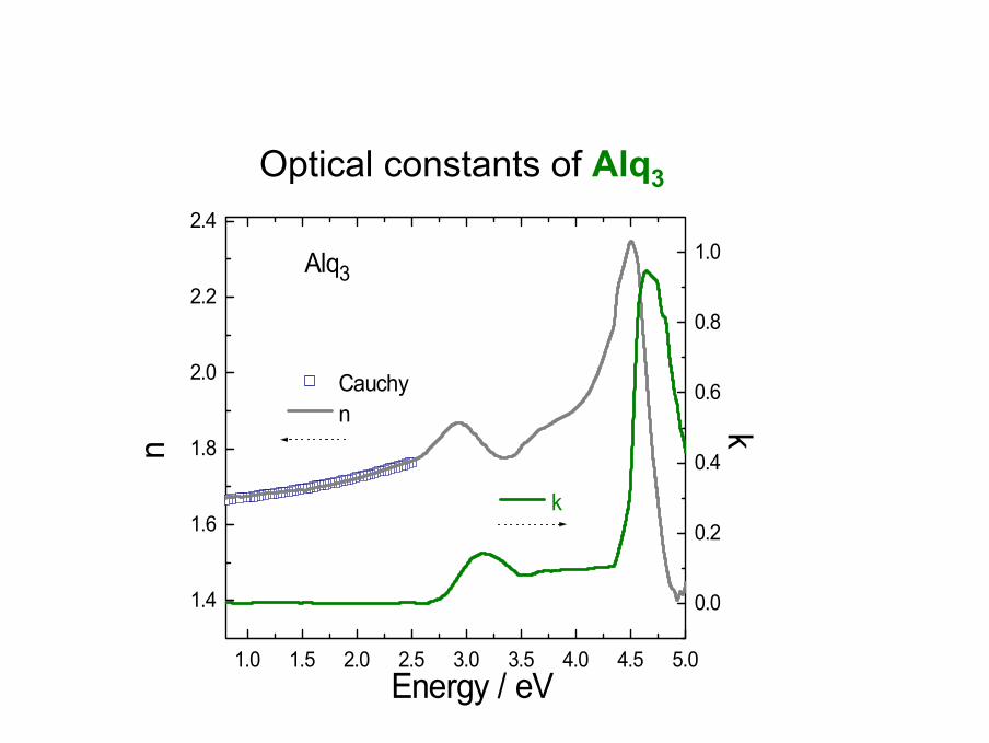
1.0 1.5 2.0 2.5 3.0 3.5 4.0 4.5 5.0
1.4
1.6
1.8
2.0
2.2
2.4
0.0
0.2
0.4
0.6
0.8
1.0
Cauchy n k
Alq3
n
Energy / eV
k
Optical constants of Alq3
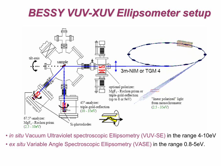
BESSY VUVBESSY VUV--XUV XUV EllipsometerEllipsometer setupsetup
• in situ Vacuum Ultraviolet spectroscopic Ellipsometry (VUV-SE) in the range 4-10eV• ex situ Variable Angle Spectroscopic Ellipsometry (VASE) in the range 0.8-5eV.
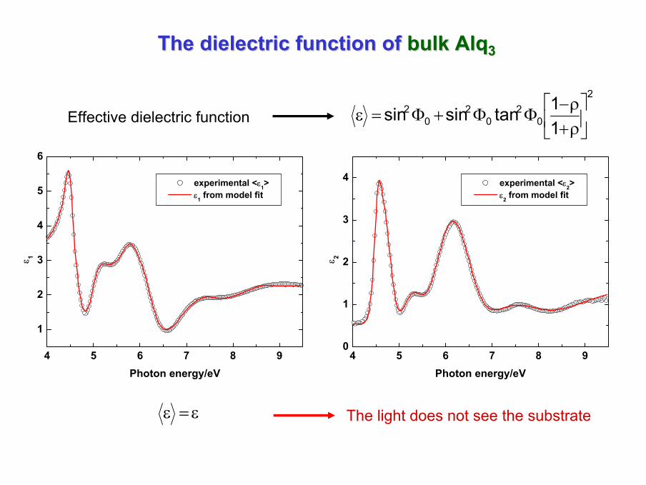
The dielectric function of The dielectric function of bulk Alqbulk Alq33
2
02
02
02
11tansinsin
ρ+ρ−
ΦΦ+Φ=ε
4 5 6 7 8 9
1
2
3
4
5
6
ε 1
Photon energy/eV
experimental <ε1> ε1 from model fit
4 5 6 7 8 90
1
2
3
4
ε 2
Photon energy/eV
experimental <ε2> ε2 from model fit
Effective dielectric function
ε=ε The light does not see the substrate
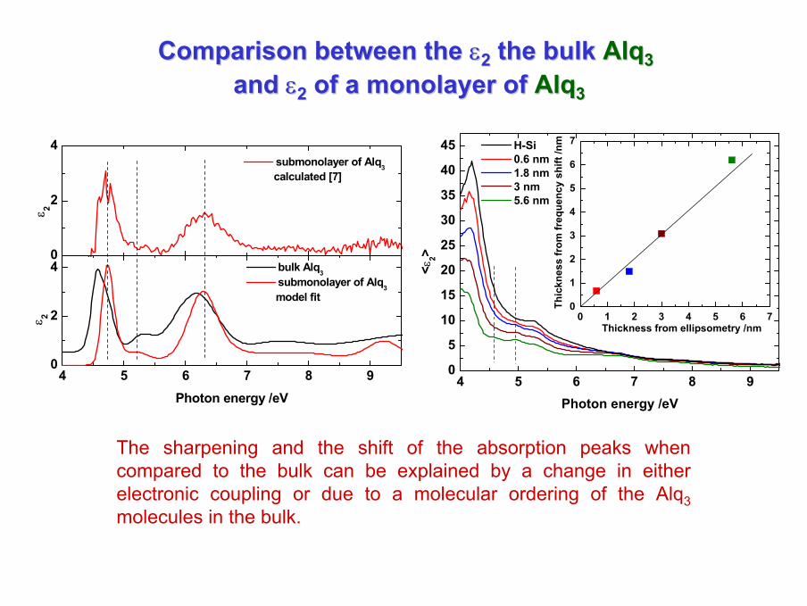
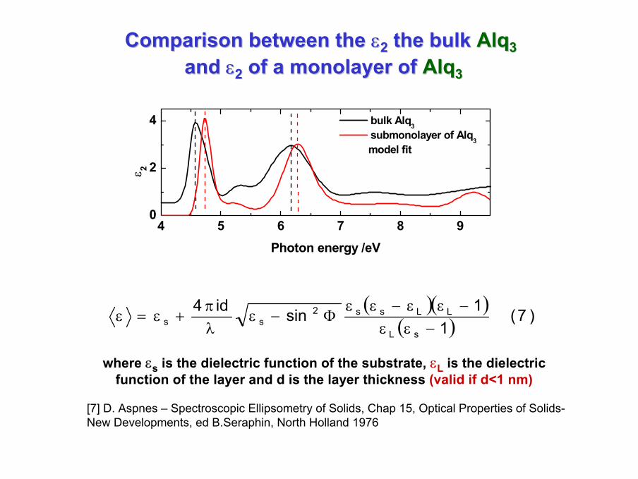
Comparison between the Comparison between the εε22 the bulk the bulk AlqAlq33and and εε22 of a monolayer of of a monolayer of AlqAlq33
4 5 6 7 8 90
5
10
15
20
25
30
35
40
45
0 1 2 3 4 5 6 70
1
2
3
4
5
6
7
<ε2>
Photon energy /eV
H-Si 0.6 nm 1.8 nm 3 nm 5.6 nm
Thic
knes
s fr
om fr
eque
ncy
shift
/nm
Thickness from ellipsometry /nm
4 5 6 7 8 90
2
4
ε 2
Photon energy /eV
bulk Alq3 submonolayer of Alq3
model fit
0
2
4
ε 2
submonolayer of Alq3 calculated [7]
The sharpening and the shift of the absorption peaks whencompared to the bulk can be explained by a change in either electronic coupling or due to a molecular ordering of the Alq3molecules in the bulk.
4 5 6 7 8 90
2
4
ε 2
Photon energy /eV
bulk Alq3 submonolayer of Alq3
model fit
Comparison between the Comparison between the εε22 the bulk the bulk AlqAlq33and and εε22 of a monolayer of of a monolayer of AlqAlq33
where εs is the dielectric function of the substrate, εL is the dielectric function of the layer and d is the layer thickness (valid if d<1 nm)
( )( )( ) )7(
11sinid4
sL
LLss2ss −εε
−εε−εεΦ−ε
λπ
+ε=ε
[7] D. Aspnes – Spectroscopic Ellipsometry of Solids, Chap 15, Optical Properties of Solids-New Developments, ed B.Seraphin, North Holland 1976
1 2 3 4 5
-20
-10
0
10
20
30
1.8 2.0 2.2 2.4 2.6
0.2
0.4
0.6
0.8
Energy /eV
[110]
DiMe-PTCDI
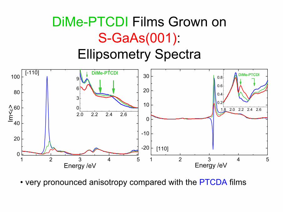
DiMe-PTCDI Films Grown on S-GaAs(001):
Ellipsometry Spectra
1 2 3 4 50
20
40
60
80
100
2.0 2.2 2.4 2.60
3
6
9
Im<ε
>
Energy /eV
[-110] DiMe-PTCDI
• very pronounced anisotropy compared with the PTCDA films
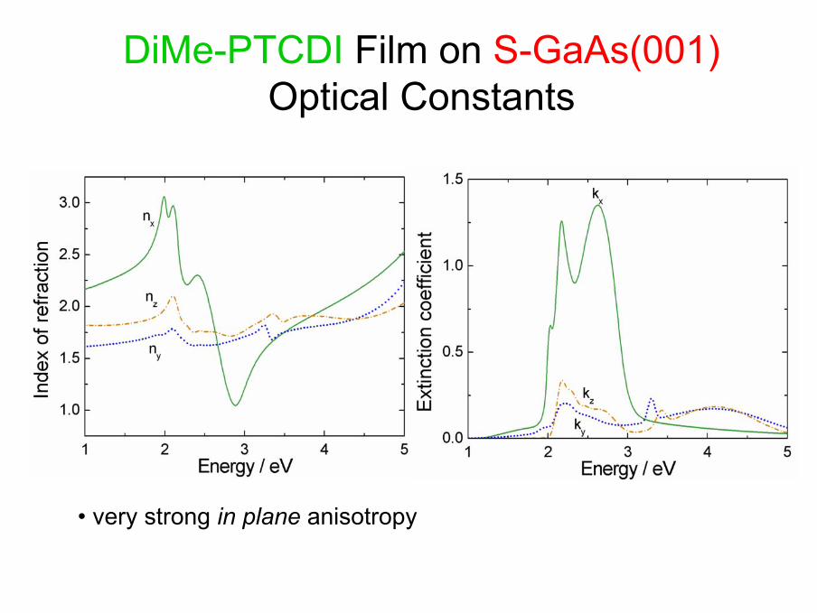
DiMe-PTCDI Film on S-GaAs(001)Optical Constants
• very strong in plane anisotropy
![= ntq;fNl];tuh tpj;ah ke;jph; Nkdpiyg; gs;sp · 1@cosθ ` a2 12 @cos2 θ ffffffffffffffffffffffffffff v u u t = 1@cosθ ` a2 sin2 θ ffffffffffffffffffffffffffff v u u t ...](https://static.fdocument.org/doc/165x107/5c02561d09d3f252338de26f/-ntqfnltuh-tpjah-kejph-nkdpiyg-gssp-1cos-a2-12-cos2-ffffffffffffffffffffffffffff.jpg)