MSP430-CCRF development board User's manual - Olimex · PDF fileMSP430-CCRF development board...
18
MSP430-CCRF development board User's manual All boards produced by Olimex are ROHS compliant Revision C, July 2013 OLIMEX Ltd, All rights reserved Page 1
Transcript of MSP430-CCRF development board User's manual - Olimex · PDF fileMSP430-CCRF development board...
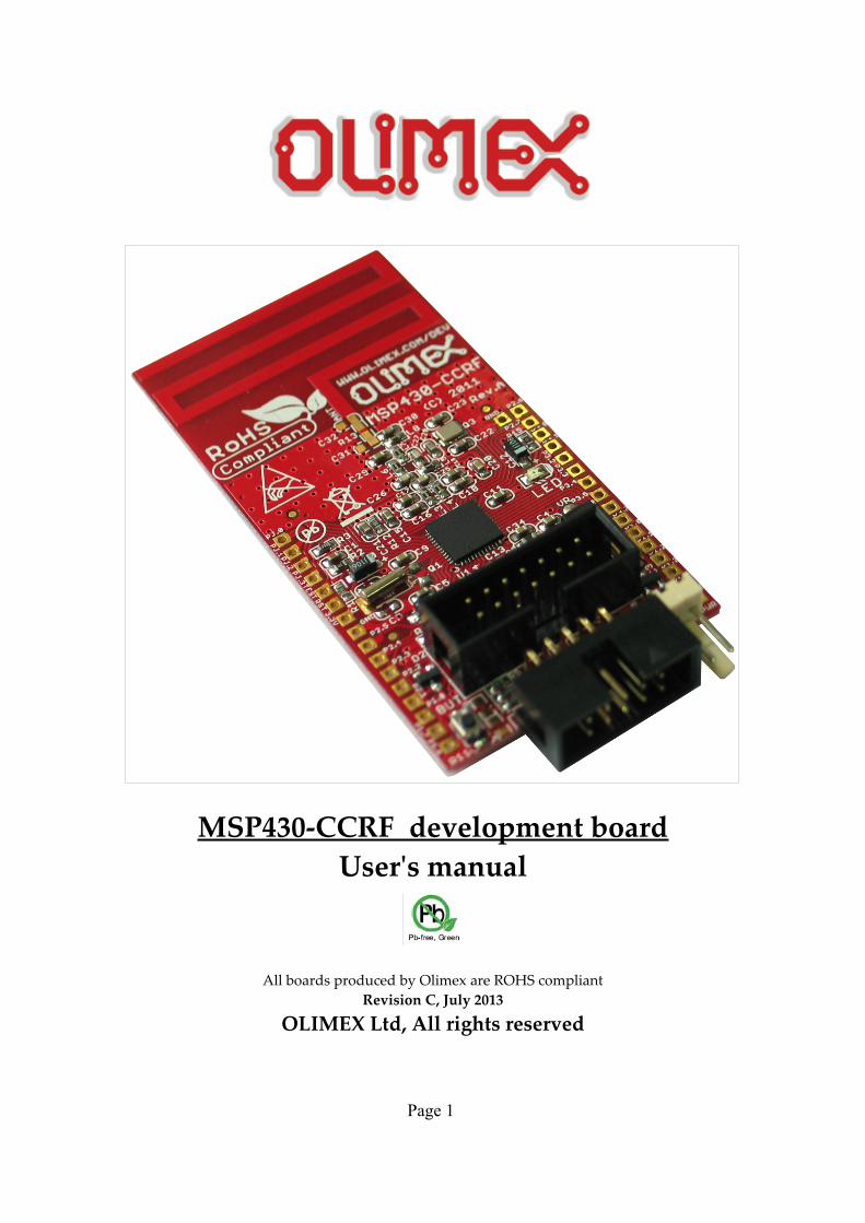
MSP430-CCRF development board User's manual
All boards produced by Olimex are ROHS compliantRevision C, July 2013
OLIMEX Ltd, All rights reserved
Page 1
INTRODUCTION:
MSP430-CCRF is development board with CC430F5137IRGZ microcontrol-ler by Texas Instruments. This ultra-low-power microcontroller has integrated CC1101 RF transceiver. The board has also UEXT, which can be modified as device or host. MSP430-CCRF can communicate with other boards with integrated CC1101 RF transceiver via radio connection.
BOARD FEATURES:
Microcontroller: CC430F5137IRGZ
JTAG
UEXT
PWR jack for 2 x 1.5V AA batteries
On-board voltage regulator
On-bard pcb antenna
Supported radio frequencies bands 868/915 MHz – software selectable. By default – 868 MHz.
Maximal permissible distance between two MSP430-CCRF boards depends on RF chip's output power, data transfer rate and the selected radio frequency band. For more information, see the table below.
User button
Status LED
RTC crystal
Extension pin holes for most of the microcontroller pins
FR-4, 1.00 mm, soldermask, component print
Dimensions: 78.49 x 39.12mm (3.09 x 1.54")
RF Frequency Output Power Data Rate Measured Distance
868MHz 10dBm 1.2kBaud 155m
868MHz 10dBm 38.4kBaud 110m
868MHz 10dBm 250kBaud 85m
915MHz 10dBm 1.2kBaud 140m
915MHz 10dBm 38.4kBaud 100m
915MHz 10dBm 250kBaud 60m
This measurements were taken via using “RF Connection_toggle LED” demo softwareloaded at two alike MSP430-CCRF boards!
Page 2
ELECTROSTATIC WARNING:
The MSP430-CCRF board is shipped in protective anti-static packaging. The boardmust not be subject to high electrostatic potentials. General practice for workingwith static sensitive devices should be applied when working with this board.
BOARD USE REQUIREMENTS:
Cables: The cable you will need depends on the programmer/debugger you would use. If you use MSP-JTAG-TINY-V2 or MSP-JTAG-ISO-MK2, you will need USB A-B cable. If you use MSP-JTAG, you will need LPT cable.
Hardware: Programmer/debugger MSP-JTAG-TINY-V2, MSP-JTAG-ISO-MK2 or other compatible programming/debugging tool.
PROCESSOR FEATURES:MSP430-CCRF board use microcontroller CC430F5137IRGZFBD100 with these features:
True System-on-Chip (SoC) for Low-Power Wireless Communication Applications
Wide Supply Voltage Range: 1.8 V to 3.6 V
Ultra-Low Power Consumption:
CPU Active Mode (AM): 160 μA/MHz
Standby Mode (LPM3 RTC Mode):2.0 μA
Off Mode (LPM4 RAM Retention): 1.0 μA
Radio in RX: 15 mA, 250 kbps, 915 MHz
MSP430™ System and Peripherals
16-Bit RISC Architecture, Extended Memory, up to 20-MHz System Clock
Wake-Up From Standby Mode in Less Than 6 μs
Flexible Power Management System with SVS and Brownout
Unified Clock System with FLL
16-Bit Timer TA0, Timer_A with Five Capture/Compare Registers
16-Bit Timer TA1, Timer_A with Three Capture/Compare Registers
Hardware Real-Time Clock
Two Universal Serial Communication Interfaces
USCI_A0 supporting UART, IrDA, SPI
USCI_B0 supporting I2C, SPI
Page 3
12-Bit A/D Converter With Internal Reference, Sample-and-Hold, and Autoscan Features
Comparator
128-bit AES Security Encryption/Decryption Coprocessor
32-Bit Hardware Multiplier
Three-Channel Internal DMA
Serial On-board Programming, No External Programming Voltage Needed
Embedded Emulation Module (EEM)
High-Performance Sub-1-GHz RF Transceiver Core
Wide Supply Voltage Range: 2.0 V to 3.6 V
Frequency Bands: 300 MHz to 348 MHz, 389 MHz to 464 MHz, and 779 MHz to 928 MHz.
Programmable Data Rate From 0.6 kBaud to 500 kBaud
High Sensitivity (-117 dBm at 0.6 kBaud, -111 dBm at 1.2 kBaud, 315 MHz, 1% Packet Error Rate)
Excellent Receiver Selectivity and Blocking Performance
Programmable Output Power Up to +12 dBm for All Supported Frequencies
2-FSK, 2-GFSK, and MSK Supported as well as OOK and Flexible ASK Shaping
Flexible Support for Packet-Oriented Systems: On-Chip Support for Sync Word Detection, Address Check, Flexible Packet Length, and Automatic CRC Handling
Support for Automatic Clear Channel Assessment (CCA) Before Transmitting (for Listen-Before-Talk Systems)
Digital RSSI Output
Suited for Systems Targeting Compliance With EN 300 220 (Europe) and FCC CFR Part 15 (US)
Suited for Systems Targeting Compliance With Wireless M-Bus Standard EN 13757-4:2005
Support for Asynchronous and Synchronous Serial Receive/Transmit Mode for Backward Compatibility With Existing Radio Communication Protocols
Page 4
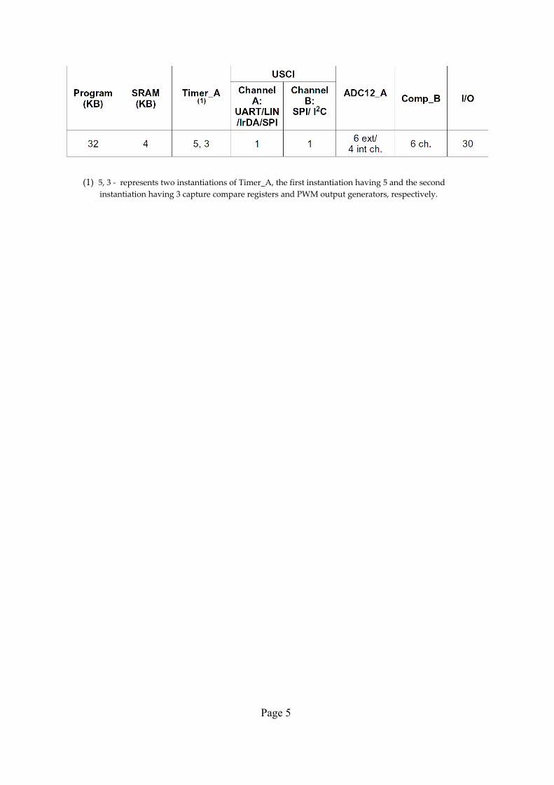
(1) 5, 3 - represents two instantiations of Timer_A, the first instantiation having 5 and the second instantiation having 3 capture compare registers and PWM output generators, respectively.
Page 5
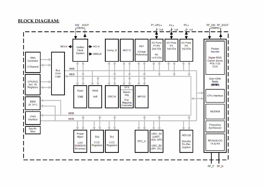
BLOCK DIAGRAM:
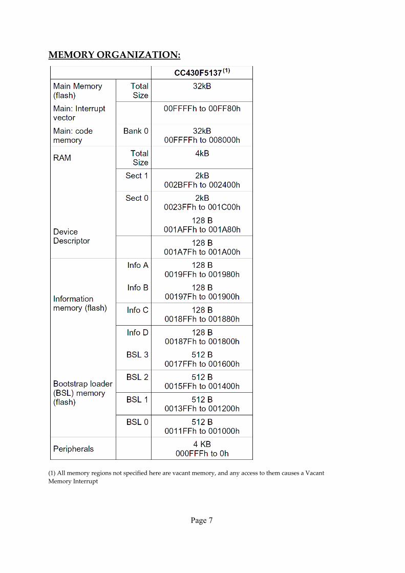
MEMORY ORGANIZATION:
(1) All memory regions not specified here are vacant memory, and any access to them causes a VacantMemory Interrupt
Page 7
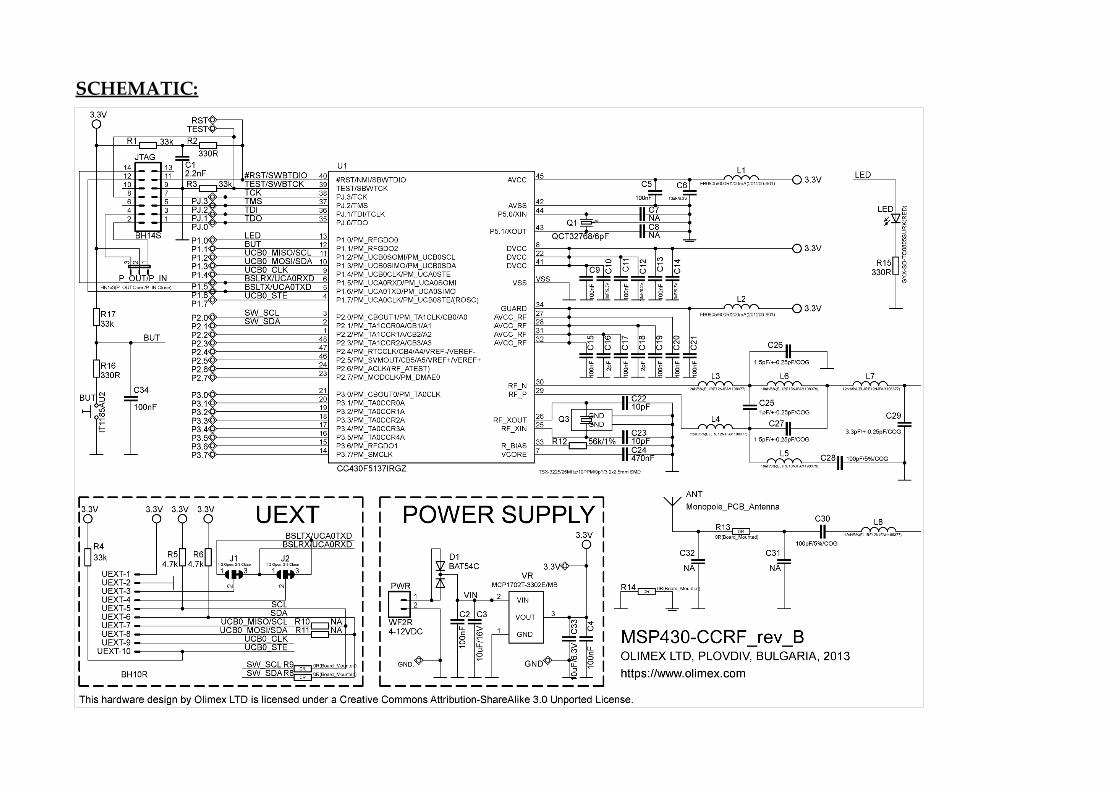
SCHEMATIC:
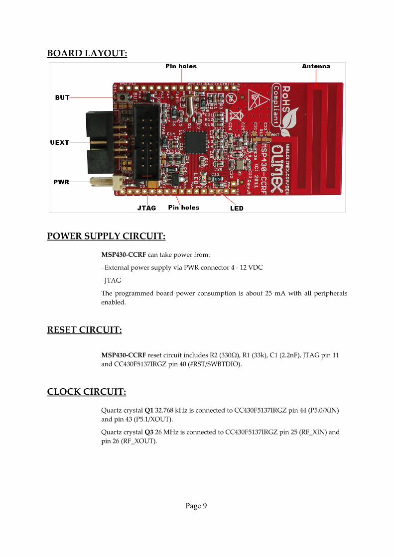
BOARD LAYOUT:
POWER SUPPLY CIRCUIT:
MSP430-CCRF can take power from:
–External power supply via PWR connector 4 - 12 VDC
–JTAG
The programmed board power consumption is about 25 mA with all peripheralsenabled.
RESET CIRCUIT:
MSP430-CCRF reset circuit includes R2 (330Ω), R1 (33k), C1 (2.2nF), JTAG pin 11 and CC430F5137IRGZ pin 40 (#RST/SWBTDIO).
CLOCK CIRCUIT:
Quartz crystal Q1 32.768 kHz is connected to CC430F5137IRGZ pin 44 (P5.0/XIN) and pin 43 (P5.1/XOUT).
Quartz crystal Q3 26 MHz is connected to CC430F5137IRGZ pin 25 (RF_XIN) and pin 26 (RF_XOUT).
Page 9
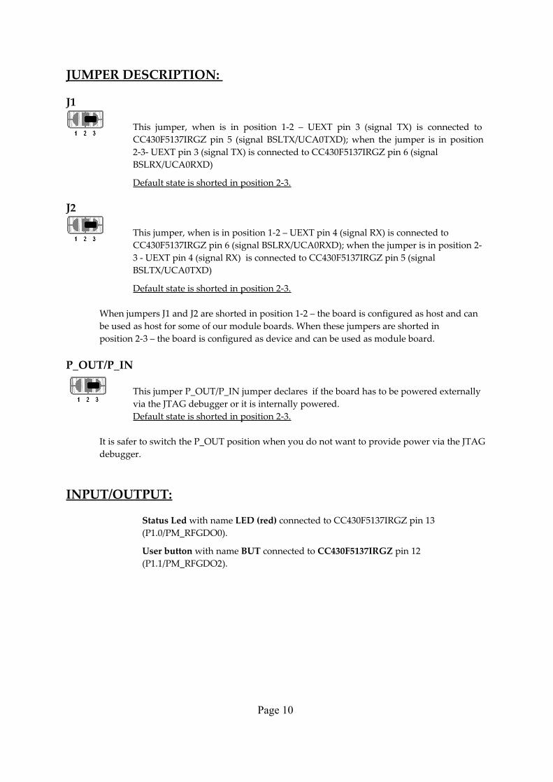
JUMPER DESCRIPTION:
J1
This jumper, when is in position 1-2 – UEXT pin 3 (signal TX) is connected to CC430F5137IRGZ pin 5 (signal BSLTX/UCA0TXD); when the jumper is in position 2-3- UEXT pin 3 (signal TX) is connected to CC430F5137IRGZ pin 6 (signal BSLRX/UCA0RXD)
Default state is shorted in position 2-3.
J2
This jumper, when is in position 1-2 – UEXT pin 4 (signal RX) is connected to CC430F5137IRGZ pin 6 (signal BSLRX/UCA0RXD); when the jumper is in position 2-3 - UEXT pin 4 (signal RX) is connected to CC430F5137IRGZ pin 5 (signal BSLTX/UCA0TXD)
Default state is shorted in position 2-3.
When jumpers J1 and J2 are shorted in position 1-2 – the board is configured as host and can be used as host for some of our module boards. When these jumpers are shorted in position 2-3 – the board is configured as device and can be used as module board.
P_OUT/P_IN
This jumper P_OUT/P_IN jumper declares if the board has to be powered externally via the JTAG debugger or it is internally powered. Default state is shorted in position 2-3.
It is safer to switch the P_OUT position when you do not want to provide power via the JTAGdebugger.
INPUT/OUTPUT:
Status Led with name LED (red) connected to CC430F5137IRGZ pin 13 (P1.0/PM_RFGDO0).
User button with name BUT connected to CC430F5137IRGZ pin 12 (P1.1/PM_RFGDO2).
Page 10
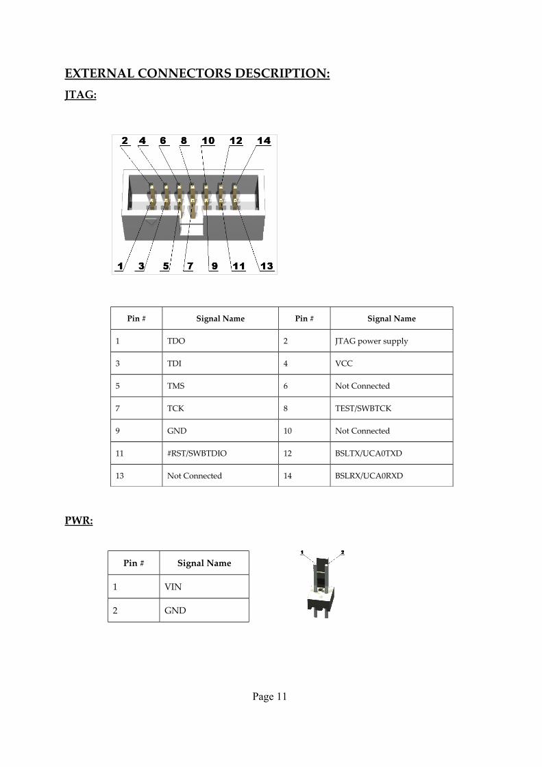
EXTERNAL CONNECTORS DESCRIPTION:JTAG:
Pin # Signal Name Pin # Signal Name
1 TDO 2 JTAG power supply
3 TDI 4 VCC
5 TMS 6 Not Connected
7 TCK 8 TEST/SWBTCK
9 GND 10 Not Connected
11 #RST/SWBTDIO 12 BSLTX/UCA0TXD
13 Not Connected 14 BSLRX/UCA0RXD
PWR:
Pin # Signal Name
1 VIN
2 GND
Page 11
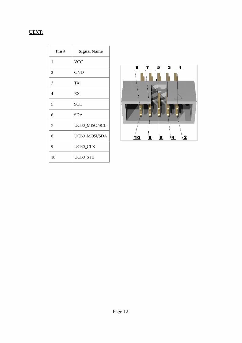
UEXT:
Pin # Signal Name
1 VCC
2 GND
3 TX
4 RX
5 SCL
6 SDA
7 UCB0_MISO/SCL
8 UCB0_MOSI/SDA
9 UCB0_CLK
10 UCB0_STE
Page 12
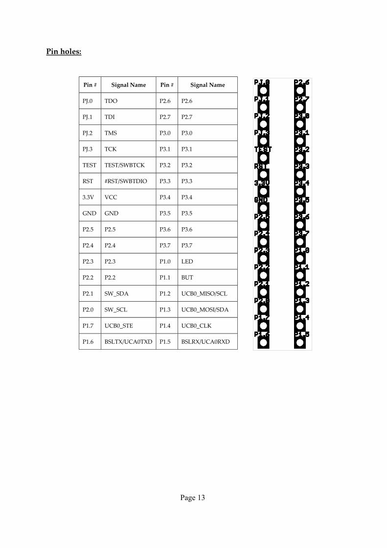
Pin holes:
Pin # Signal Name Pin # Signal Name
PJ.0 TDO P2.6 P2.6
PJ.1 TDI P2.7 P2.7
PJ.2 TMS P3.0 P3.0
PJ.3 TCK P3.1 P3.1
TEST TEST/SWBTCK P3.2 P3.2
RST #RST/SWBTDIO P3.3 P3.3
3.3V VCC P3.4 P3.4
GND GND P3.5 P3.5
P2.5 P2.5 P3.6 P3.6
P2.4 P2.4 P3.7 P3.7
P2.3 P2.3 P1.0 LED
P2.2 P2.2 P1.1 BUT
P2.1 SW_SDA P1.2 UCB0_MISO/SCL
P2.0 SW_SCL P1.3 UCB0_MOSI/SDA
P1.7 UCB0_STE P1.4 UCB0_CLK
P1.6 BSLTX/UCA0TXD P1.5 BSLRX/UCA0RXD
Page 13
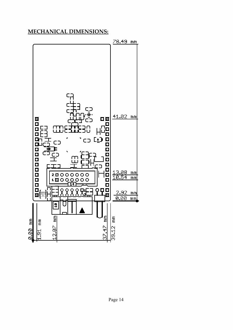
MECHANICAL DIMENSIONS:
Page 14
AVAILABLE DEMO SOFTWARE:
There is a number of example for MSP430-CCRF compatible with IAR Embedded Workbench for MSP430 v4.21. Unfortunately, it is possible that the code would not compile under IAR for MSP430 v5.xx due to incompatibility between versions. The code is available at the MSP430-CCRF web page atOLIMEX LTD web site.
Blinking Led sourced by DCO
Blinking Led sourced by RTC
Blinking Led sourced by RTC and USART Echo
Toggle LED when BUT is pressed
RF Connection_ press BUT
RF Connection_toggle LED
Page 15
ORDER CODE:
MSP430-CCRF - assembled and tested board
How to order?
You can order to us directly or by any of our distributors.Check our web https://www.olimex.com for more info.
Revision history:
Board's revision: Rev. A, May 2011
Rev. B, Mart 2013
1. Added P_OUT/P_IN jumper to solve power short-circuits when the board is powered from the JTAG
2. The RTC capacitors C7 and C8 have been removed and the internal CCRF capacitors have been used instead.
3. The drill size under U1 is changed from 1.5mm to 0.6mm
4. Removed arrows from the bottom silk
5. Power supply white print changed from 3-12VDC to 4-12VDC
Manual's revision: Rev. A, June 2011
- in BOARD FEATURES - added Supported radio frequencies bands, Maximal permissible distance between two MSP430-CCRF boards, RTC crystal and “Not typical power jack” changed to “PWR jack for 2 x 1.5V AA batteries“
Rev. B, November 2011
- BOARD FEATURES – added is table which describes maximal permissible distance between two MSP430-CCRF boards versus different RF settings.
- SCHEMATIC – is updated to last version – with changed C22 and C23 values from 15pF to 10pF.
- AVAILABLE DEMO SOFTWARE – “RF Connection_ press BUT to send a packet and toggle LED when packet is
Page 16
received” is changed to “RF Connection_ press BUT”. “RF Connection_toggle LED” was added.
Rev. C, November 2013
- SCHEMATIC – revision B of the schematic added
- updated supported debuggers list
- improved the spelling of the document
- added more info about revisions
- expanded warranty and support page
Page 17
For product support, hardware information and error reports mail to: [email protected]. Note that we are primarily a hardware company and our software support is limited.
Please consider reading the paragraph below about the warranty of Olimex products.
All goods are checked before they are sent out. In the unlikely event that goods are faulty, they must be returned, to OLIMEX at the address listed on your order invoice.
OLIMEX will not accept goods that have clearly been used more than the amount needed to
evaluate their functionality.
If the goods are found to be in working condition, and the lack of functionality is a
result of lack of knowledge on the customers part, no refund will be made, but the goods
will be returned to the user at their expense.
All returns must be authorized by an RMA Number. Email [email protected] for
authorization number before shipping back any merchandise. Please include your name,
phone number and order number in your email request.
Returns for any unaffected development board, programmer, tools, and cables permitted
within 7 days from the date of receipt of merchandise. After such time, all sales are
considered final. Returns of incorrect ordered items are allowed subject to a 10%
restocking fee. What is unaffected? If you hooked it to power, you affected it. To be
clear, this includes items that have been soldered to, or have had their firmware
changed. Because of the nature of the products we deal with (prototyping electronic
tools) we cannot allow returns of items that have been programmed, powered up, or
otherwise changed post shipment from our warehouse.
All returned merchandise must be in its original mint and clean condition. Returns on
damaged, scratched, programmed, burnt, or otherwise 'played with' merchandise will not be
accepted.
All returns must include all the factory accessories which come with the item. This
includes any In-Circuit-Serial-Programming cables, anti-static packing, boxes, etc.
With your return, enclose your PO#. Also include a brief letter of explanation of why the
merchandise is being returned and state your request for either a refund or an exchange.
Include the authorization number on this letter, and on the outside of the shipping box.
Please note: It is your responsibility to ensure that returned goods reach us. Please use
a reliable form of shipping. If we do not receive your package we will not be held
liable.
Shipping and handling charges are not refundable. We are not responsible for any shipping
charges of merchandise being returned to us or returning working items to you.
The full text might be found at https://www.olimex.com/wiki/GTC#Warranty for future reference.
Page 18