Development Board EPC9106 Quick Start Guide · Development Board EPC9106 Quick Start Guide 150 W/8...
10
Development Board EPC9106 Quick Start Guide 150 W/8 Ω Class-D Amplifier Revision D
Transcript of Development Board EPC9106 Quick Start Guide · Development Board EPC9106 Quick Start Guide 150 W/8...
Development Board EPC9106 Quick Start Guide150 W/8 Ω Class-D Amplifier
Revision D
QUICK START GUIDE Demonstration System EPC9106
2 | | EPC – EFFICIENT POWER CONVERSION CORPORATION | WWW.EPC-CO.COM | COPYRIGHT 2017
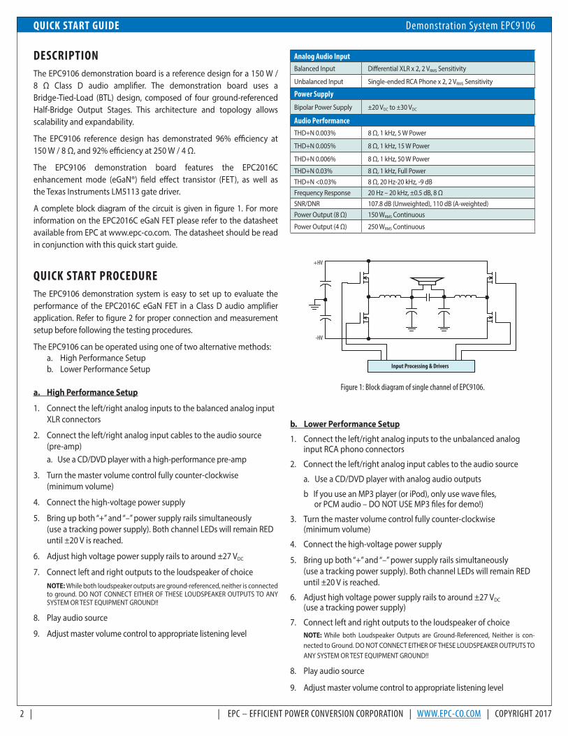
DESCRIPTION The EPC9106 demonstration board is a reference design for a 150 W / 8 Ω Class D audio amplifier. The demonstration board uses a Bridge-Tied-Load (BTL) design, composed of four ground-referenced Half-Bridge Output Stages. This architecture and topology allows scalability and expandability.
The EPC9106 reference design has demonstrated 96% efficiency at 150 W / 8 Ω, and 92% efficiency at 250 W / 4 Ω.
The EPC9106 demonstration board features the EPC2016C enhancement mode (eGaN®) field effect transistor (FET), as well as the Texas Instruments LM5113 gate driver.
A complete block diagram of the circuit is given in figure 1. For more information on the EPC2016C eGaN FET please refer to the datasheet available from EPC at www.epc-co.com. The datasheet should be read in conjunction with this quick start guide.
QUICK START PROCEDURE The EPC9106 demonstration system is easy to set up to evaluate the performance of the EPC2016C eGaN FET in a Class D audio amplifier application. Refer to figure 2 for proper connection and measurement setup before following the testing procedures.
The EPC9106 can be operated using one of two alternative methods:a. High Performance Setupb. Lower Performance Setup
a. High Performance Setup
1. Connect the left/right analog inputs to the balanced analog input XLR connectors
2. Connect the left/right analog input cables to the audio source (pre-amp)
a. Use a CD/DVD player with a high-performance pre-amp
3. Turn the master volume control fully counter-clockwise (minimum volume)
4. Connect the high-voltage power supply
5. Bring up both “+” and “–” power supply rails simultaneously (use a tracking power supply). Both channel LEDs will remain RED until ±20 V is reached.
6. Adjust high voltage power supply rails to around ±27 VDC
7. Connect left and right outputs to the loudspeaker of choice NOTE: While both loudspeaker outputs are ground-referenced, neither is connected
to ground. DO NOT CONNECT EITHER OF THESE LOUDSPEAKER OUTPUTS TO ANY SYSTEM OR TEST EQUIPMENT GROUND!!
8. Play audio source
9. Adjust master volume control to appropriate listening level
Analog Audio InputBalanced Input Differential XLR x 2, 2 VRMS Sensitivity
Unbalanced Input Single-ended RCA Phone x 2, 2 VRMS Sensitivity
Power Supply
Bipolar Power Supply ±20 VDC to ±30 VDC
Audio PerformanceTHD+N 0.003% 8 Ω, 1 kHz, 5 W Power
THD+N 0.005% 8 Ω, 1 kHz, 15 W Power
THD+N 0.006% 8 Ω, 1 kHz, 50 W Power
THD+N 0.03% 8 Ω, 1 kHz, Full PowerTHD+N <0.03% 8 Ω, 20 Hz-20 kHz, -9 dBFrequency Response 20 Hz – 20 kHz, ±0.5 dB, 8 ΩSNR/DNR 107.8 dB (Unweighted), 110 dB (A-weighted)Power Output (8 Ω) 150 WRMS Continuous
Power Output (4 Ω) 250 WRMS Continuous
Figure 1: Block diagram of single channel of EPC9106.
+HV
-HV
Input Processing & Drivers
b. Lower Performance Setup
1. Connect the left/right analog inputs to the unbalanced analog input RCA phono connectors
2. Connect the left/right analog input cables to the audio source
a. Use a CD/DVD player with analog audio outputs
b If you use an MP3 player (or iPod), only use wave files, or PCM audio – DO NOT USE MP3 files for demo!)
3. Turn the master volume control fully counter-clockwise (minimum volume)
4. Connect the high-voltage power supply
5. Bring up both “+” and “–” power supply rails simultaneously (use a tracking power supply). Both channel LEDs will remain RED until ±20 V is reached.
6. Adjust high voltage power supply rails to around ±27 VDC (use a tracking power supply)
7. Connect left and right outputs to the loudspeaker of choice NOTE: While both Loudspeaker Outputs are Ground-Referenced, Neither is con-
nected to Ground. DO NOT CONNECT EITHER OF THESE LOUDSPEAKER OUTPUTS TO ANY SYSTEM OR TEST EQUIPMENT GROUND!!
8. Play audio source
9. Adjust master volume control to appropriate listening level
QUICK START GUIDE Demonstration System EPC9106
EPC – EFFICIENT POWER CONVERSION CORPORATION | WWW.EPC-CO.COM | COPYRIGHT 2017 | | 3
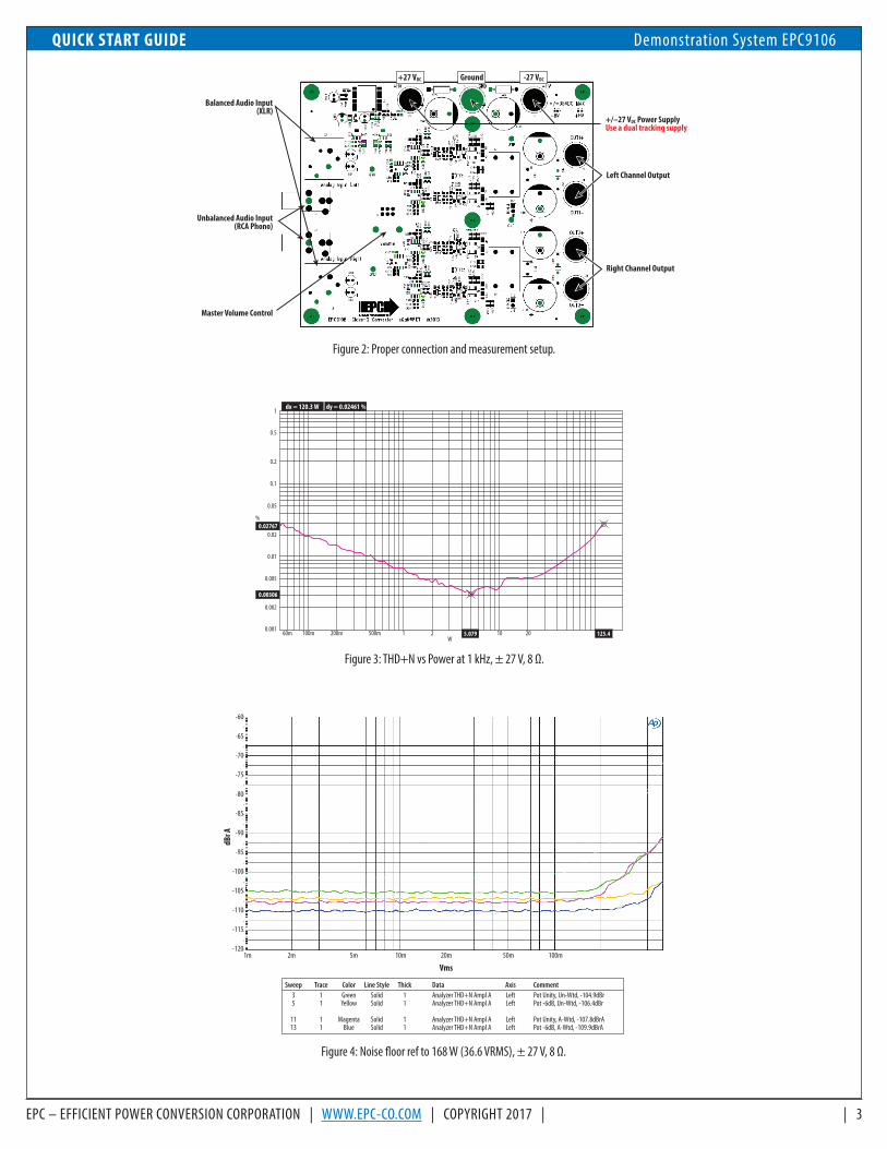
Figure 2: Proper connection and measurement setup.
Right Channel Output
Master Volume Control
Unbalanced Audio Input(RCA Phono)
Balanced Audio Input(XLR)
Left Channel Output
+/–27 VDC Power SupplyUse a dual tracking supply
Ground+27 VDC -27 VDC
Figure 3: THD+N vs Power at 1 kHz, ± 27 V, 8 Ω.
Figure 4: Noise floor ref to 168 W (36.6 VRMS), ± 27 V, 8 Ω.
1
0.5
0.2
0.1
0.05
%
0.02
0.01
0.005
0.002
0.00160m 100m 200m 500m 1 2
W10 20
dx = 120.3 W
0.02767
0.00306
5.079 125.4
dy = 0.02461 %
dBr A
1m 2m 5m 10m 20m 50m 100m
Vms
Sweep Trace Color Line Style Thick Data Axis Comment 3 1 Green Solid 1 Analyzer THD+N Ampl A Left Pot Unity, Un-Wtd, -104.9dBr 5 1 Yellow Solid 1 Analyzer THD+N Ampl A Left Pot -6dB, Un-Wtd, -106.4dBr
11 1 Magenta Solid 1 Analyzer THD+N Ampl A Left Pot Unity, A-Wtd, -107.8dBrA 13 1 Blue Solid 1 Analyzer THD+N Ampl A Left Pot -6dB, A-Wtd, -109.9dBrA
-60
-65
-70
-75
-80
-85
-90
-95
-100
-105
-110
-115
-120
QUICK START GUIDE Demonstration System EPC9106
4 | | EPC – EFFICIENT POWER CONVERSION CORPORATION | WWW.EPC-CO.COM | COPYRIGHT 2017
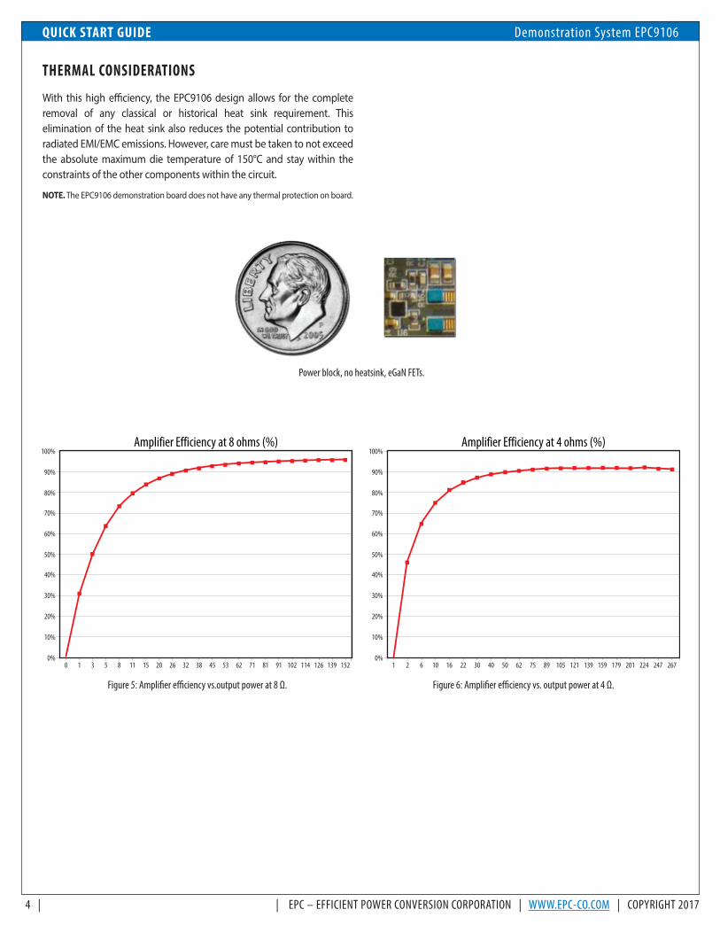
THERMAL CONSIDERATIONS
With this high efficiency, the EPC9106 design allows for the complete removal of any classical or historical heat sink requirement. This elimination of the heat sink also reduces the potential contribution to radiated EMI/EMC emissions. However, care must be taken to not exceed the absolute maximum die temperature of 150°C and stay within the constraints of the other components within the circuit.
NOTE. The EPC9106 demonstration board does not have any thermal protection on board.
Power block, no heatsink, eGaN FETs.
Figure 6: Amplifier efficiency vs. output power at 4 Ω.Figure 5: Amplifier efficiency vs.output power at 8 Ω.
0%
10%
20%
30%
40%
50%
60%
70%
80%
90%
100%
0
Amplifier Efficiency at 8 ohms (%)
1 3 5 8 11 15 20 26 32 38 45 53 62 71 81 91 102 114 126 139 1520%
10%
20%
30%
40%
50%
60%
70%
80%
90%
100%
1
Amplifier Efficiency at 4 ohms (%)
2 6 10 16 22 30 40 50 62 75 89 105 121 139 159 179 201 224 247 267
QUICK START GUIDE Demonstration System EPC9106
EPC – EFFICIENT POWER CONVERSION CORPORATION | WWW.EPC-CO.COM | COPYRIGHT 2017 | | 5
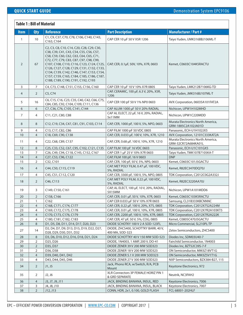
Table 1 : Bill of Material
Item Qty Reference Part Description Manufacturer / Part #
1 10 C1, C9, C37, C70, C78, C106, C140, C143, C163, C164 CAP CER 10 µF 50 V X5R 1206 Taiyo Yuden, UMK316BBJ106ML-T
2 67
C2, C3, C8, C10, C14, C20, C28, C29, C30, C38, C39, C41, C43, C54, C55, C56, C57, C58, C59, C60, C62, C63, C64, C65, C71, C72, C77, C79, C83, C87, C97, C98, C99, C107, C108, C110, C116, C123, C124, C125, C126, C127, C128, C129, C131, C132, C133, C134, C139, C142, C146, C147, C153, C154, C157, C159, C165, C184, C185, C186, C187, C188, C189, C190, C191, C192, C193
CAP, CER, 0.1µF, 50V, 10%, X7R, 0603 Kemet, C0603C104K5RACTU
3 7 C4, C73, C148, C151, C155, C156, C160 CAP CER 10 µF 10 V 10% X7R 0805 Taiyo Yuden, LMK212B7106KG-TD
4 2 C5, C74 CAP, CERAMIC, 100 µF, 6.3 V, 20%, X5R, 1206 Taiyo Yuden, JMK316BJ107ML-T
5 16 C6, C15, C16, C23, C35, C40, C42, C66, C75, C84, C85, C92, C104, C109, C111, C136 CAP CER 100 pF 50 V 1% NP0 0603 AVX Corporation, 06035A101FAT2A
6 6 C7, C36, C76, C105, C141, C144 CAP ALUM 1000 µF 50 V 20% RADIAL Nichicon, UPW1H102MHD
7 4 C11, C21, C80, C88 CAP AL ELECT, 22 µF, 16 V, 20%, RADIAL, 5x11MM Nichicon, UPW1C220MDD
8 8 C12, C19, C34, C47, C81, C91, C103, C114 CAP, CER, 1000 pF, 100 V, 5%, NPO, 0603 Murata Electronics North America, GRM-1885C2A102JA01D
9 4 C13, C17, C82, C86 CAP FILM 1000 pF 50 VDC 0805 Panasonic, ECH-U1H102JX5 10 4 C18, C69, C90, C138 CAP, CER, 0.033 µF, 100 V, 10%, X7R, 1210 AVX Corporation, 12101C333KAT2A
11 4 C22, C68, C89, C137 CAP, CER, 0.68 µF, 100 V, 10%, X7R, 1210 Murata Electronics North America, GRM-32CR72A684KA01L
12 8 C25, C33, C52, C67, C95, C102, C121, C135 CAP FILM 100 pF 16 VDC 0603 Panasonic, ECH-U1C101GX5 13 7 C26, C49, C94, C118, C145, C152, C167 CAP CER 1 µF 25 V 10% X7R 0603 Taiyo Yuden, TMK107B7105KA-T 14 4 C27, C53, C96, C122 CAP, FILM 100 pF, 16 V 0603 DNP15 2 C32, C101 CAP, CER, 100 pF, 50 V, 5%, NP0, 0603 Kemet, C0603C101J5GACTU
16 4 C44, C50, C115, C119 CAP, MET POLY FILM, 0.47 µF, 100 VDC, 5%, RADIAL Kemet, R82EC3470DQ70J
17 4 C45, C51, C112, C120 CAP, CER, 3300 pF, 100 V, 5%, NPO, 0805 TDK Corporation, C2012C0G2A332J
18 2 C46, C113 CAP, MET POLY FILM, 0.22 µF, 100 VDC, 5%, RADIAL Kemet, R82EC3220AA70J
19 3 C149, C150, C161 CAP, AL ELECT, 100 µF, 10 V, 20%, RADIAL, 5X15MM Nichicon, UPW1A101MDD6
20 2 C158, C166 CAP, CER, 0.01 µF, 50 V, 10%, X7R, 0603 Kemet, C0603C103K5RACTU 21 1 C162 CAP CER 0.033 µF 50 V 10% X7R 0603 Samsung, CL31B333KBCNNNC22 4 C168, C171, C174, C177 CAP, CER, 0.22 µF, 100 V, 20%, X7S, 0805 TDK Corporation, C2012X7S2A224M 23 4 C169, C172, C175, C178 CAP, CER, 0.01 µF, 100 V, 10%, X7R, 0805 TDK Corporation, C2012X7R2A103KT5 24 4 C170, C173, C176, C179 CAP, CER, 2200 pF, 100 V, 10%, X7R, 0805 TDK Corporation, C2012X7R2A222K 25 4 C180, C181, C182, C183 CAP, CER, 47 pF, 50 V, 5%, COG, 0805 Kemet, C0805C470J5GACTU 26 8 D1, D5, D8, D11, D14, D17, D20, D23 DIODE SCHOTKY 100 V 2 A SOD-123FL Micro Commercial, SL210PL-TP
27 14 D2, D4, D7, D9, D13, D15, D19, D22, D27, D28, D29, D30, D31, D32
DIODE, ZHCS400, SCHOTTKY BARR, 40 V, 400 MA, SOD-323 Zetex Semiconductors, ZHCS400
28 8 D3, D6, D10, D12, D16, D18, D21, D24 DIODE SCHOTTKY 40 V 150 MW SOD-523 Diodes Inc, SDM03U40-7 29 2 D25, D26 DIODE, 1N4003, 1 AMP, 200 V, DO-41 Fairchild Semiconductor, 1N4003 30 2 D35, D37 DIODE ZENER 39 V 200 MW SOD323 Diodes Inc, BZT52C39S-7-F31 2 D36, D38 DIODE ZENER 18 V 200 MW SOD323 ON Semiconductor, MM3Z18VT1G32 4 D39, D40, D41, D42 DIODE ZENER 5.1 V 200 MW SOD323 ON Semiconductor, MM3Z5V1T1G33 4 D43, D44, D45, D46 DIODE ZENER 27 V 300 MW SOD323 NXP Semiconductors, BZX384-B27, 115
34 2 J1, J5 Jack, Phono RCA, w/Switch, R/A, PCB Mount Keystone Electronics, 972
35 2 J2, J6 XLR Connectors 3P FEMALE HORIZ PIN 1 & GRD SEPARATE Neutrik, NC3FAH2
36 4 J3, J7, J9, J11 JACK, BINDING BANANA, INSUL, RED Keystone Electronics, 7006 37 3 J4, J8, J10 JACK, BINDING BANANA, INSUL, BLACK Keystone Electronics, 7007 38 2 J12, J13 CONN, HDR, 2x1, 0.100, GOLD FLASH FCI, 68001-202HLF
QUICK START GUIDE Demonstration System EPC9106
6 | | EPC – EFFICIENT POWER CONVERSION CORPORATION | WWW.EPC-CO.COM | COPYRIGHT 2017
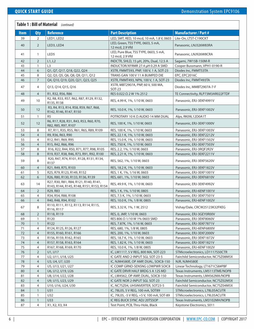
Table 1 : Bill of Material (continued)
Item Qty Reference Part Description Manufacturer / Part #39 2 LED1, LED2 LED, SMT, RED, 10 mcd, 10 mA, 1.8 V, 0603 Lite-On, LTST-C190CKT
40 2 LED3, LED4 LED, Green, TSS TYPE, 0603, 5 mA, 12 mcd, 2.9 Vfd Panasonic, LNJ326W83RA
41 1 LED5 LED, Pure Blue, TSS TYPE, 0603, 5 mA, 12 mcd, 2.9 Vfd Panasonic, LNJ926W8CRA
42 2 L1, L2 INDCTR, SHLD, 15 µH, 20%, Dual, 12.5 A Sagami, 7W15B-150M-R 43 1 L3 INDUCTOR/XFRMR 27.4 µH 0.29 A SMD Cooper Bussmann, VPH1-0190-R 44 6 Q1, Q7, Q17, Q18, Q22, Q24 XSTR, FMMT593, PNP, 100 V, 1 A, SOT-23 Diodes Inc, FMMT53TA45 8 Q2, Q3, Q5, Q6, Q8, Q9, Q11, Q12 TRANS GAN 100 V 11 A BUMPED DIE EPC, EPC2016C 46 7 Q4, Q10, Q19, Q20, Q21, Q23, Q25 XSTR, FMMT493, NPN, 100 V, 1 A, SOT-23 Diodes Inc, FMMT493TA
47 4 Q13, Q14, Q15, Q16 XSTR, MBT2907A, PNP, 60 V, 500 MA, SOT-23 Diodes Inc, MMBT2907A-7-F
48 4 R1, R32, R56, R86 RES 0.022 Ω 2 W 1% 2512 TE Connectivity, RLP73M3AR022FTDF
49 10 R2, R8, R33, R57, R62, R87, R129, R132, R135, R138 RES, 4.99 K, 1%, 1/10 W, 0603 Panasonic, ERJ-3EKF4991V
50 12 R3, R4, R13, R14, R58, R59, R67, R68, R142, R146, R147, R150 RES, 10.0 K, 1%, 1/10 W, 0603 Panasonic, ERJ-3EKF1002V
51 1 R5 POTROTARY 10 K Ω AUDIO 14 MM DUAL Alps, RK09L12D0A1T
52 12 R6, R17, R28, R31, R43, R53, R60, R70, R82, R85, R97, R107 RES, 100 K, 1%, 1/10 W, 0603 Panasonic, ERJ-3EKF1000V
53 8 R7, R11, R35, R55, R61, R65, R89, R109 RES, 100 K, 1%, 1/10 W, 0603 Panasonic, ERJ-3EKF1003V 54 4 R9, R36, R63, R90 RES, 22.1 K, 1%, 1/10 W, 0603 Panasonic, ERJ-3EKF2212V 55 4 R12, R41, R69, R95 RES, 15.0 K, 1%, 1/10 W, 0603 Panasonic, ERJ-3EKF1502V 56 4 R15, R42, R66, R96 RES, 750 K, 1%, 1/10 W, 0603 Panasonic, ERJ-3EKF7503V 57 8 R16, R22, R44, R50, R71, R77, R98, R105 RES, 2.2, 1%, 1/10 W, 0603 Panasonic, ERJ-3RQF2R2V 58 8 R19, R37, R38, R46, R73, R91, R92, R100 RES, 2.21 K, 1%, 1/10 W, 0603 Panasonic, ERJ-3EKF2211V
59 8 R20, R47, R74, R101, R128, R131, R134, R137 RES, 562, 1%, 1/10 W, 0603 Panasonic, ERJ-3EKF5620V
60 4 R21, R49, R75, R103 RES, 18.2 K, 1%, 1/10 W, 0603 Panasonic, ERJ-3EKF1822V 61 5 R25, R79, R123, R149, R152 RES, 1 K, 1%, 1/16 W, 0603 Panasonic, ERJ-3EKF1001V 62 6 R26, R80, R130, R133, R136, R139 RES, 681, 1%, 1/10 W, 0603 Panasonic, ERJ-3EKF6810V
63 14 R27, R30, R81, R84, R121, R140, R141, R143, R144, R145, R148, R151, R153, R154 RES, 49.9 K, 1%, 1/10 W, 0603 Panasonic, ERJ-3EKF4992V
64 2 R29, R83 RES, 1 K, 1%, 1/10 W, 0805 Panasonic, ERJ-6ENF1001V 65 4 R34, R54, R88, R108 RES, 7.5 K, 1%, 1/10 W, 0603 Panasonic, ERJ-3EKF7501V 66 4 R40, R48, R94, R102 RES, 10.0 K, 1%, 1/8 W, 0805 Panasonic, ERJ-6ENF1002V
67 8 R110, R111, R112, R113, R114, R115, R116, R117 RES, 3.32 K, 1%, 1 W, 2512 Vishay/Dale, CRCW25123K32FKEG
68 2 R118, R119 RES, 0, JMP, 1/10 W, 0603 Panasonic, ERJ-3GEY0R00V 69 1 R120 RES 806 Ω 1/10 W 1% 0603 SMD Panasonic, ERJ-3EKF8060V 70 1 R122 RES, 7.87K, 1%, 1/16 W, 0603 Panasonic, ERJ-3EKF7871V 71 4 R124, R125, R126, R127 RES, 680, 1%, 1/8 W, 0805 Panasonic, ERJ-6ENF6800V 72 4 R155, R160, R161, R166 RES, 200, 1%, 1/10 W, 0603 Panasonic, ERJ-3EKF2000V73 4 R156, R159, R162, R165 RES, 18.7 K, 1%, 1/10 W, 0603 Panasonic, ERJ-3EKF1872V74 4 R157, R158, R163, R164 RES, 1.82 K, 1%, 1/10 W, 0603 Panasonic, ERJ-3EKF1821V75 4 R167, R168, R169, R170 RES, 10.0 K, 1%, 1/8 W, 0805 Panasonic, ERJ-6ENF1002V76 2 U1, U17 IC, LM1117, 5 V REG, 800 MA, SOT-223 STMicroelectronics, LD1117S50CTR 77 4 U2, U11, U18, U25 IC GATE AND 2-INPUT SGL SOT-23-5 Fairchild Semiconductor, NC7SZ08M5X 78 4 U3, U4, U7, U20 IC, NJM4580E, OP AMP, DUAL, SOIC8-150 NJR, NJM4580E 79 4 U5, U13, U21, U27 IC COMP GRND-SENSNG LOWPWR SOIC8 Linear Technology, LT1671CS8#PBF 80 4 U6, U12, U19, U26 IC GATE DRVR HALF BRDG 5 A 12S MD Texas Instruments, LM5113TME/NOPB 81 4 U8, U14, U22, U28 IC, LM4562, OP AMP, DUAL, SOIC8-150 Texas Instruments, LM4562MA/NOPB 82 4 U9, U15, U23, U29 IC GATE NOR 2-INPUT SGL SOT-23 Fairchild Semiconductor, NC7SZ02M5X 83 4 U10, U16, U24, U30 IC, NC7SZ04, UHSINVERTER, SOT23-5 Fairchild Semiconductor, NC7SZ04M5X 84 1 U31 IC, 78L05, 5 V REG, 100 mA, SOT89 STMicroelectronics, L78L05ACUTR 85 1 U32 IC, 79L05, -5 V REG, +5 V, 100 mA, SOT-89 STMicroelectronics, L79L05ACUTR 86 1 U33 IC REG BUCK SYNC ADJ 20TSSOP Texas Instruments, LM3102MH/NOPB 87 4 X1, X2, X3, X4 Test Point, PCB, Thru-Hole, Black Keystone Electronics, 5011
QUICK START GUIDE Demonstration System EPC9106
EPC – EFFICIENT POWER CONVERSION CORPORATION | WWW.EPC-CO.COM | COPYRIGHT 2017 | | 7
VCC
= (-
HV
+ 5)
V
Ch1
Out
+
Ch1
Out
-
From
OV
/UV
Det
ect
7VF
+HV
-HV
+5V
-5V
SW
1+
nER
R1
nER
R1
nER
R1
-HV
1
+HV
1
IN-1
+
nER
R1
nER
R1
+HV
1
-HV
1
IN-1
-
IN-1
+
IN-1
-
OU
T1+
SW
1-
-HV
1
+HV
1
-HV
1
+HV
1
OU
T1-
7VF
+HV
-HV
+5V
-5V
nER
R1
7VF
+HV
-HV
+5V
-5V
+5V
-5V
-HV
1
+HV
-HV
1
-HV
1
-HV
1
VC
C1
VC
C1
-HV
1
-HV
1
-5V
+5V
-HV
1
-HV
1-H
V1
VC
C1
VC
C1
VC
C1
VC
C1
7VF
-HV
1
-HV
1
-HV
1
-HV
1
-HV
1
VC
C1
VC
C1
-HV
1
-5V
-HV
1
+5V
-HV
1
-HV
1-H
V1
VC
C1
VC
C1
-HV
1
VC
C1
-HV
1
VC
C1
-HV
1
-HV
1
+5V
+5V
-HV
+HV
+HV
D9
ZHC
S40
0S
OD
-323
21
D44
BZX
384-
B27
27V
SO
D-3
23
21
C17
022
00pF
100V
DC
0805
R50
2.2
0603
C28
0.1u
F06
03
D5
SL2
10P
L-TP
SO
D12
3FL
21
R44
2.2
0603
J4B
LAC
K
C14
0.1u
F06
03
C45
3300
pF10
0V08
05
C63
0.1u
F06
03
C16
100p
F06
03
R37
2.21
K06
03
R16
020
006
03
+C
3610
00uF
50V
PW
Ser
ies
R28
100
0603
C33
100p
F06
03
R47
562
0603
C65
0.1u
F06
03
R12
94.
99K
0603
C52
100p
F06
03
C57
0.1u
F06
03
C54
0.1u
F06
03
C42
100p
F06
03
D10
SD
M03
U40
SO
D-5
23
21
J12
1
3
C18
047
pF08
05
C27
DN
P06
03
D6
SD
M03
U40
SO
D-5
23
21
U14
C
LM4562
48
C56
0.1u
F06
03
C20
0.1u
F06
03
R13
24.
99K
0603
R30
49.9
K06
03
R17
100
0603
C17
10.
22uF
100V
DC
0805
D2
ZHC
S40
0S
OD
-323
21
D43
BZX
384-
B27
27V
SO
D-3
23
21
D1
SL2
10P
L-TP
SO
D12
3FL
21
C58
0.1u
F06
03U
3C
NJM4580E
48
+C
510
0uF
6.3V
1206
+
C21
22uF 16V
PW
Ser
ies
R16
2.2
0603 C
3710
uF
1206
50V
R26
681
0603
C66
100p
F06
03
R9
22.1
K06
03
C59
0.1u
F06
03
R15
520
006
03
+- U7A N
JM45
80E
321
Q2
EP
C20
16C
1
23456789
1011
R33
4.99
K06
03
R48
10K
0805
R16
7D
NP
0805
U8C
LM4562
48
+- U4A N
JM45
80E
321
C13
1000
pF08
05
R15
918
.7K
0603
R3
10K
0603
C41
0.1u
F06
03
Q23
FMM
T493
TAS
OT-
23N
PN
1
23
R25
1K 0603
CW
R5A
PO
T-10
K-D
UA
L
1
2
3
C16
90.
01uF
100V
DC
0805
C30
0.1u
F06
03
R40
10K
0805
LED
1R
ED
LE
DLE
D06
03
2 1
C25
100p
F06
03
C32
100p
F06
03
C60
0.1u
F06
03
C39
0.1u
F06
03
+
C11
22uF 16V
PW
Ser
ies
C19
1
0.1u
F06
03
R38
2.21
K06
03
C68
0.68
uF
100V
DC
1210
C47
1000
pF06
03
R22
2.2
0603
R32
0.02
2
2512
1W
VC
C
GN
DN/
C
U16
NC
7SZ0
42
3
4
5
1
R13
068
106
03D
29ZH
CS
400
SO
D-3
23
2 1
C29
0.1u
F06
03
Q3
EP
C20
16C
1
23456789
1011
J3RE
D
C19
1000
pF06
03
U1LM
1117
-5V SO
T-22
3
GND1
TAB
4V
IN3
VO
UT
2
+- U8A LM
4562
321
R15
618
.7K
0603
J12
1 2
Q4
FMM
T493
TA
SO
T-23
NP
N1
23
D39
MM
3Z5V
1T1G
5.1V
SO
D-3
23
21
C17
1000
pF08
05
R27
49.9
K06
03
C69
0.03
3uF
100V
DC
1210
R20
562
0603 R
133
681
0603
C34
1000
pF10
0V06
03
R8
4.99
K06
03
C10
0.1u
F
0603
50V
DC
VC
C
GN
DN/
C
U10
NC
7SZ0
42
3
4
5
1
Q1
FMM
T593
TA
SO
T-23
PN
P1
2 3
U6
LM51
13TM
E
12-B
UM
P-U
SM
D
HI
B4
LIA
4
HO
LD
1
HO
HD
2
HB
D3
HS
C1
LOL
A1
LOH
B1
VSSA2
VDDC4
VDDA3
HS
D4
Q6
EP
C20
16C
1
23456789
1011
R16
8D
NP
0805
C18
0.03
3uF
100V
DC
1210
C35
100p
F06
03
R7
100K
0603
Q22
FMM
T593
TAS
OT-
23P
NP
1
23
C67
100p
F06
03
+- U4B N
JM45
80E
567
R2
4.99
K06
03
GN
D
VC
C U9
NC
7SZ0
2
2 345
1
+- U3A N
JM45
80E
321
C64
0.1u
F06
03
R42
750K
0603
R46
2.21
K06
03
D12
SD
M03
U40
SO
D-5
23
21
R35
100K
0603
C17
20.
01uF
100V
DC
0805
C1
10uF
1206
50V
C18
147
pF08
05
R15
750K
0603
C16
80.
22uF
100V
DC
0805
Q13
MM
BT2
907A
SO
T23
PN
P1
2 3
R13
10K
0603
GN
D
VC
C U2
NC
7SZ0
81 2 3
45
L1B
15uH
7W15
B
34
C19
0
0.1u
F06
03
R31
100
0603
C2
0.1u
F
0603
50V
DC
R15
81.
82K
0603
C46
0.22
uF
FILM
100V
DC
C51
3300
pF10
0V08
05
C55
0.1u
F06
03
C49
1uF
0603
25V
DC
C15
100p
F06
03
R54
7.5K
0603
R34
7.5K
0603
U4C
NJM4580E
48
CA
SE
R5C
PO
T-10
K-D
UA
L7
8
R14
10K
0603
MH
MH
CA
SE
J2N
C3F
AH
2
1
3
2
4 56
R43
100
0603
R53
100
0603
D40
MM
3Z5V
1T1G
5.1V
SO
D-3
23
21
R55
100K
0603
C18
40.
1uF
0603
R4
10K
0603
C9
10uF
1206
50V
C44
0.47
uF
FILM
100V
DC
U5
LT16
71
V+
1
IN+
2
IN-
3
V-
4LA
TCH
5G
ND
6Q
OU
T7
QO
UT
8
R12
568
008
05
R15
71.
82K
0603
D30
ZHC
S40
0S
OD
-323
2 1
R29
1K 0805
U13
LT16
71
V+
1
IN+
2
IN-
3
V-
4LA
TCH
5G
ND
6Q
OU
T7
QO
UT
8
Q14
MM
BT2
907A
SO
T23
PN
P1
2 3
C23
100p
F06
03
C4
10uF
0805
10V
R12
15.0
K06
03
C18
50.
1uF
0603
D8
SL2
10P
L-TP
SO
D12
3FL
21
U12
LM51
13TM
E
12-B
UM
P-U
SM
D
HI
B4
LIA
4
HO
LD
1
HO
HD
2
HB
D3
HS
C1
LOL
A1
LOH
B1
VSSA2
VDDC4
VDDA3
HS
D4
D11
SL2
10P
L-TP
SO
D12
3FL
21
Q5
EP
C20
16C
1
23456789
1011
R19
2.21
K06
03
R36
22.1
K06
03
R13
156
206
03
+- U14
A
LM45
62
321
D4
ZHC
S40
0S
OD
-323
21
GN
D
VC
C U11
NC
7SZ0
81 2 3
45
C62
0.1u
F06
03
C22
0.68
uF
100V
DC
1210
R11
100K
0603
R12
856
206
03
C3
0.1u
F06
03
C53
DN
P06
03
R1
0.02
2
2512
1WC
1210
00pF
0603
R41
15.0
K06
03
R21
18.2
K06
03
R49
18.2
K06
03
R6
100
0603
GN
D
VC
C U15
NC
7SZ0
2
2 345
1
C43
0.1u
F06
03
R12
468
008
05
C6
100p
F06
03
C17
322
00pF
100V
DC
0805
C40
100p
F06
03
D3
SD
M03
U40
SO
D-5
23
21
C26
1uF
0603
25V
DC
+-U
14B
LM45
62
567
C50
0.47
uF
FILM
100V
DC
+-U
8B
LM45
62
567
+C
710
00uF
50V
PW
Ser
ies
D7
ZHC
S40
0S
OD
-323
21
L1A
15uH
7W15
B
12
C8
0.1u
F06
03
C38
0.1u
F
0603
50V
DC
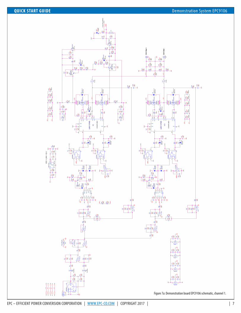
Figure 7a: Demonstration board EPC9106 schematic, channel 1.
QUICK START GUIDE Demonstration System EPC9106
8 | | EPC – EFFICIENT POWER CONVERSION CORPORATION | WWW.EPC-CO.COM | COPYRIGHT 2017
VCC
= (-
HV
+ 5)
V
Ch2
Out
-
Ch2
Out
+
From
OV
/UV
Det
ect
7VF
+HV
-HV
+5V
-5V
nER
R2
nER
R2
+HV
2
nER
R2
nER
R2
+HV
2
-HV
2
SW
2-
IN-2
+
IN-2
-
IN-2
+
IN-2
-
-HV
2
+HV
2
-HV
2
+HV
2
SW
2+
nER
R2
-HV
2
OU
T2-
OU
T2+
7VF
+HV
-HV
+5V
-5V
nER
R2
7VF
+HV
-HV
+5V
-5V
+5V
-5V
-HV
2
-HV
2
-HV
2
-HV
2
VC
C2
VC
C2
-HV
2
-HV
2
-HV
2
-HV
2-H
V2
VC
C2
VC
C2
VC
C2
7VF
-HV
2
-HV
2
-HV
2
-HV
2
-HV
2
VC
C2
VC
C2
-HV
2
-HV
2
-HV
2
-HV
2-H
V2
VC
C2
VC
C2
-HV
2
VC
C2
-HV
2
VC
C2
-HV
2
-HV
2
+5V
-5V
+5V
-5V
+5V
+5V
+HV
-HV
VC
C2
+HV
+HV
C19
3
0.1u
F06
03
R16
41.
82K
0603
C18
70.
1uF
0603
R65
100K
0603
U21
LT16
71
V+
1
IN+
2
IN-
3
V-
4LA
TCH
5G
ND
6Q
OU
T7
QO
UT
8
C75
100p
F06
03
Q9
EP
C20
16C
1
23456789
1011
GN
D
VC
C U25
NC
7SZ0
81 2 3
45C
109
100p
F06
03
C10
70.
1uF
0603
50V
DC
Q10
FMM
T493
TA
SO
T-23
NP
N1
23
D22
ZHC
S40
0S
OD
-323
21
R13
668
106
03
C78
10uF
1206
50V
R73
2.21
K06
03
C12
60.
1uF
0603
+- U28
A
LM45
62
321
C71
0.1u
F
0603
50V
DC
R10
9
100K
0603
Q11
EP
C20
16C
1
23456789
1011
R77
2.2
0603
R10
156
206
03
R10
0
2.21
K06
03
R69
15.0
K06
03
C13
80.
033u
F
100V
DC
1210
C11
30.
22uF
FILM
100V
DC
U27
LT16
71
V+
1
IN+
2
IN-
3
V-
4LA
TCH
5G
ND
6Q
OU
T7
QO
UT
8
+C
7410
0uF
6.3V
1206
Q8
EP
C20
16C
1
23456789
1011
C82
1000
pF08
05
Q12
EP
C20
16C
1
23456789
1011
R16
218
.7K
0603
C13
10.
1uF
0603
C81
1000
pF06
03
D18
SD
M03
U40
SO
D-5
23
21
R96
750K
0603
C11
0
0.1u
F06
03
D19
ZHC
S40
0S
OD
-323
21
MH
MH
CA
SE
J6N
C3F
AH
2
1
3
2
4 56
C17
50.
01uF
100V
DC
0805
U26
LM51
13TM
E
12-B
UM
P-U
SM
D
HI
B4
LIA
4
HO
LD
1
HO
HD
2
HB
D3
HS
C1
LOL
A1
LOH
B1
VSSA2
VDDC4
VDDA3
HS
D4
Q24
FMM
T593
TAS
OT-
23P
NP
1
23
C10
110
0pF
0603
R12
668
008
05
R13
84.
99K
0603
R13
756
206
03
J7RE
D
C11
60.
1uF
0603
C95
100p
F06
03
C11
1
100p
F06
03
C11
81u
F06
0325
VD
C
R16
31.
82K
0603
R74
562
0603
R88
7.5K
0603
R63
22.1
K06
03
C10
210
0pF
0603
+-U
22B
LM45
62
567
R58
10K
0603
U20
C
NJM4580E
48
R17
0D
NP
0805
+
C80
22uF 16V
PW
Ser
ies
D45
BZX
384-
B27
27V
SO
D-3
23
21
C12
90.
1uF
0603
CW
R5B
PO
T-10
K-D
UA
L
4
5
6
C92
100p
F06
03
R57
4.99
K06
03
R84
49.9
K06
03
C13
6
100p
F06
03
D20
SL2
10P
L-TP
SO
D12
3FL
21
R91
2.21
K06
03
C11
4
1000
pF06
03
D16
SD
M03
U40
SO
D-5
23
21
R13
54.
99K
0603
+C
7610
00uF
50V
PW
Ser
ies
R98
2.2
0603
J13
1 2
C13
70.
68uF
100V
DC
1210
C90
0.03
3uF
100V
DC
1210
C17
80.
01uF
100V
DC
0805
R60
100
0603
C12
70.
1uF
0603
R75
18.2
K06
03
D23
SL2
10P
L-TP
SO
D12
3FL
21
C13
20.
1uF
0603
U22
C
LM4562
48
U17LM
1117
-5V SO
T-22
3
GND1
TAB
4V
IN3
VO
UT
2
D14
SL2
10P
L-TP
SO
D12
3FL
21
C94
1uF
0603
25V
DC
U28
C
LM4562
48
+- U7B N
JM45
80E
567
+- U22
A
LM45
62
321
R62
4.99
K06
03
C11
50.
47uF
FILM
100V
DC
R67
10K
0603
C84
100p
F06
03
GN
D
VC
C U23
NC
7SZ0
2
2 345
1
R79
1K 0603
C87
0.1u
F06
03
C18
347
pF08
05
C10
610
uF
1206
50V
R87
4.99
K06
03
R81
49.9
K06
03
L2B
15uH
7W15
B
34
C99
0.1u
F06
03
GN
D
VC
C U29
NC
7SZ0
2
2 345
1
C13
510
0pF
0603
C97
0.1u
F06
03
R13
968
106
03
R83
1K 0805
D24
SD
M03
U40
SO
D-5
23
21
D21
SD
M03
U40
SO
D-5
23
21
L2A
15uH
7W15
B
12
J52
1
3
R59
10K
0603
C12
50.
1uF
0603
C17
70.
22uF
100V
DC
0805
R95
15.0
K06
03
C13
40.
1uF
0603
C12
033
00pF
100V
0805
D17
SL2
10P
L-TP
SO
D12
3FL
21
D42
MM
3Z5V
1T1G
5.1V
SO
D-3
23
21
C10
310
00pF
100V
0603
R10
210
K08
05
LED
2R
ED
LE
DLE
D06
03
2 1
R10
7
100
0603
VC
C
GN
DN/
C
U24
NC
7SZ0
42
3
4
5
1
D46
BZX
384-
B27
27V
SO
D-3
23
21
R71
2.2
0603
C17
622
00pF
100V
DC
0805
C19
2
0.1u
F06
03
Q25
FMM
T493
TAS
OT-
23N
PN
1
23
C10
4
100p
F06
03
C12
80.
1uF
0603
D31
ZHC
S40
0S
OD
-323
2 1
C18
60.
1uF
0603
Q15
MM
BT2
907A
SO
T23
PN
P1
2 3
+
C88
22uF 16V
PW
Ser
ies
C85
100p
F06
03
R16
620
006
03
J8B
LAC
K
C86
1000
pF08
05
VC
C
GN
DN/
C
U30
NC
7SZ0
42
3
4
5
1
R86
0.02
2
2512
1W
R12
768
008
05
+- U3B N
JM45
80E
567
Q7
FMM
T593
TA
SO
T-23
PN
P1
2 3
R97
100
0603
C12
4
0.1u
F06
03
R82
100
0603
C12
2D
NP
0603
C77
0.1u
F06
03
R66
750K
0603
C17
40.
22uF
100V
DC
0805
R13
456
206
03
R89
100K
0603
C70
10uF
1206
50V
Q16
MM
BT2
907A
SO
T23
PN
P1
2 3
+C
105
1000
uF50
VP
W S
erie
s
+- U20
B
NJM
4580
E
567
C73
10uF
0805
10V
C79
0.1u
F
0603
50V
DC
D32
ZHC
S40
0S
OD
-323
2 1
D41
MM
3Z5V
1T1G
5.1V
SO
D-3
23
21
C13
30.
1uF
0603
R61
100K
0603
R68
10K
0603
D13
ZHC
S40
0S
OD
-323
21
R90
22.1
K06
03
R16
9D
NP
0805
+- U20
A
NJM
4580
E
321
R92
2.21
K06
03
C96
DN
P06
03
R10
318
.2K
0603
U7C
NJM4580E
48
R56
0.02
2
2512
1W
C72
0.1u
F06
03
GN
D
VC
C U18
NC
7SZ0
81 2 3
45
R80
681
0603
C11
90.
47uF
FILM
100V
DC
+-U
28B
LM45
62
567
R70
100
0603
R16
120
006
03
C12
110
0pF
0603
C10
8
0.1u
F06
03
R94
10K
0805
C18
247
pF08
05
R10
5
2.2
0603
C83
0.1u
F06
03
U19
LM51
13TM
E
12-B
UM
P-U
SM
D
HI
B4
LIA
4
HO
LD
1
HO
HD
2
HB
D3
HS
C1
LOL
A1
LOH
B1
VSSA2
VDDC4
VDDA3
HS
D4
R85
100
0603
C91
1000
pF06
03
R10
8
7.5K
0603
C98
0.1u
F06
03
C12
30.
1uF
0603
D15
ZHC
S40
0S
OD
-323
21
R16
518
.7K
0603
C89
0.68
uF
100V
DC
1210
C17
922
00pF
100V
DC
0805
C11
233
00pF
100V
0805
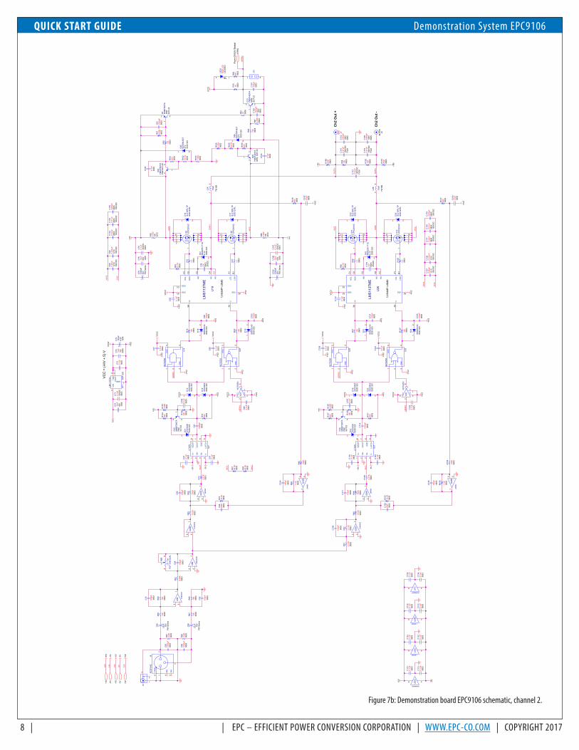
Figure 7b: Demonstration board EPC9106 schematic, channel 2.
QUICK START GUIDE Demonstration System EPC9106
EPC – EFFICIENT POWER CONVERSION CORPORATION | WWW.EPC-CO.COM | COPYRIGHT 2017 | | 9
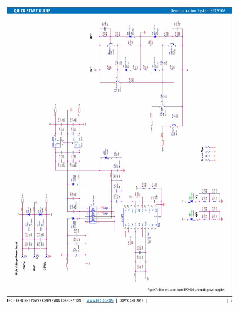
Figure 7c: Demonstration board EPC9106 schematic, power supplies.
Hig
h Vo
ltage
Pow
er In
put
+35V
dc
GN
D
-35V
dc
Gro
und
Clip
s
+HV
-HV
PVU
PVO
-5V
-7V
A
+5V
+HV
+7V
A
GN
D
+HV
+HV
-
7VF
nER
R1
nER
R2
+5V
-5V
+HV
-HV
7VF
nER
R1
nER
R2
+5V
-5V
-HV
+HV
+HV
+7V
A
+HV
-HV
7VF
-HV
+HV
+HV
-HV
D27
ZHC
S40
0S
OD
-323
21
R11
63.
32K
2512
R14
610
K06
03
C16
20.
033u
F12
06
R14
549
.9K
0603
C15
40.
1uF
0603
R14
349
.9K
0603
C16
50.
1uF
0603
50V
DC
R1190-Ohm
R11
33.
32K
2512
R12
149
.9K
0603
C15
21u
F06
0325
VD
C
Q20
FMM
T493
TA
SO
T-23
NP
N1
23
R14
049
.9K
0603
R14
149
.9K
0603
C13
90.
1uF
0603
50V
DC
R14
2
10K
0603
R12
080
606
03
R14
710
K06
03
Q18
FMM
T593
TA
SO
T-23
PN
P1
2 3
C16
71u
F06
0325
VD
C
R11
43.
32K
2512
D38
MM
3Z18
VT1
G18
VS
OD
-323
21
Q17
FMM
T593
TA
SO
T-23
PN
P1
2 3
X2
C14
010
uF
1206
50V
L3 IND
-VP
1-01
90
4
15
2
3
6
9
12
7
10
11
8
R15
2
1K 0603
R12
27.
87K
0603
+C
161
100u
F10
VP
W S
erie
s
R11
23.
32K
2512
R11
03.
32K
2512
J11
RE
D
C16
410
uF
1206
50V
R11
13.
32K
2512
+C
141
1000
uF50
VP
W S
erie
s
R11
53.
32K
2512
D36
MM
3Z18
VT1
G18
VS
OD
-323
21
C15
70.
1uF
0603
D25
1N40
03D
O-4
1
LED
3G
RN
LE
DLE
D06
03
2 1
D26
1N40
03D
O-4
1
C14
310
uF
1206
50V
D37
BZT
52C
39S
-7-F
39V
SO
D-3
23
21
X1
C14
20.
1uF
0603
50V
DC
D35
BZT
52C
39S
-7-F
39V
SO
D-3
23
21
C18
80.
1uF
0603
50V
DC
C15
80.
01uF
0603
50V
R1180-Ohm
Q21
FMM
T493
TA
SO
T-23
NP
N1
23
C14
60.
1uF
0603
R15
149
.9K
0603
C16
010
uF
0805
10V
C18
90.
1uF
0603
50V
DC
X3
R12
31K 06
03
Q19
FMM
T493
TA
SO
T-23
NP
N1
23
C15
610
uF
0805
10V
LED
4G
RN
LE
DLE
D06
03
21
R14
849
.9K
0603
U31
78L0
5S
OT8
9
GND2
Vin
3V
out
1
TAB4
J10
BLA
CK
C14
70.
1uF
0603
D28
ZHC
S40
0S
OD
-323
21
C15
510
uF
0805
10V
R15
0
10K
0603
C14
810
uF
0805
10V
+C
149
100u
F10
VP
W S
erie
s
+C
144
1000
uF50
VP
W S
erie
s
U33
LM31
02N
C1
SW
2
SW
3
VIN
4
VIN
5
BS
T6
AG
ND
7
SS
8
NC
9
NC
10G
ND
11N
C12
FDB
K13
EN
14R
ON
15V
CC
16P
GN
D17
PG
ND
18N
C19
NC
20
PAD21
U32
79L0
5S
OT8
9
GND1
Vin
2V
out
3Ta
b4
C14
51u
F06
0325
VD
C
J9RE
D
R15
349
.9K
0603
C16
60.
01uF
0603
R11
73.
32K
2512
+C
150
100u
F10
VP
W S
erie
s
C15
110
uF
0805
10V
LED
5B
lue
LED
LED
0603
2 1
R14
449
.9K
0603
C15
30.
1uF
0603
X4
R15
449
.9K
0603
R14
9
1K 0603
C16
310
uF
1206
50V
C15
90.
1uF
0603
50V
DC

Demonstration Board Notification
The EPC9106 board is intended for product evaluation purposes only and is not intended for commercial use. Replace components on the Evaluation Board only with those parts shown on the parts list (or Bill of Materials) in the Quick Start Guide. Contact an authorized EPC representative with any questions.
This board is intended to be used by certified professionals, in a lab environment, following proper safety procedures. Use at your own risk.
As an evaluation tool, this board is not designed for compliance with the European Union directive on electromagnetic compatibility or any other such directives or regulations. As board builds are at times subject to product availability, it is possible that boards may contain components or assembly materials that are not RoHS compliant. Efficient Power Conversion Corporation (EPC) makes no guarantee that the purchased board is 100% RoHS compliant.
The Evaluation board (or kit) is for demonstration purposes only and neither the Board nor this Quick Start Guide constitute a sales contract or create any kind of warranty, whether express or implied, as to the applications or products involved.
Disclaimer: EPC reserves the right at any time, without notice, to make changes to any products described herein to improve reliability, function, or design. EPC does not assume any liability arising out of the application or use of any product or circuit described herein; neither does it convey any license under its patent rights, or other intellectual property whatsoever, nor the rights of others.
EPC Products are distributed through Digi-Key.www.digikey.com
For More Information:
Please contact [email protected] your local sales representative
Visit our website: www.epc-co.com
Sign-up to receive EPC updates atbit.ly/EPCupdates or text “EPC” to 22828