LTM4653 (Rev 0) - analog.com · LTM4653 Rev 0 For more information 48V 0 0 5V,,,
32
LTM4653 1 Rev 0 For more information www.analog.com Document Feedback TYPICAL APPLICATION FEATURES DESCRIPTION EN55022B Compliant 58V, 4A Step-Down DC/DC μModule Regulator 4A, 24V Output Low EMI DC/DC μModule Regulator with Analog Output Current Indicator APPLICATIONS n Complete Low EMI Switch Mode Power Supply n EN55022 Class B Compliant n Wide Input Voltage Range: 3.1V to 58V n Up to 4A Output Current n Output Voltage Range: 0.5V ≤ V OUT ≤ 0.94 • V IN n ±1.67% Total DC Output Voltage Error Over Line, Load and Temperature (–40°C to 125°C) n Parallel and Current Share with Multiple LTM4653s n Analog Output Current Indicator n Programmable Input Voltage Limiting n Constant-Frequency Current Mode Control n Power Good Indicator and Programmable Soft-Start n Overcurrent/Overvoltage/Overtemperature Protection n 15mm × 9mm × 5.01mm BGA Package n Avionics, Industrial Control and Test Equipment n Video, Imaging and Instrumentation n 48V Telecom and Network Power Supplies n RF Systems All registered trademarks and trademarks are the property of their respective owners. Protected by U.S. Patents, including 5481178, 5705919, 5847554, 6580258. Radiated Emission Scan in a 10m Chamber LTM4653 Delivering 24V OUT at 3.5A, from 48V IN PINS NOT USED IN THIS CIRCUIT: CLKIN, PGOOD, COMPb PGDFB, SW, EXTV CC TEMP + , TEMP – , NC ISETa GND ISETb V IN SV IN V D RUN INTV CC VINREG COMPa f SET V OUT LTM4653 24V OUT , UP TO 4A I OUT ANALOG OUTPUT CURRENT INDICATOR V IMON = 0.25Ω • I OUT 10μF ×2 LOAD 124k 10nF 499Ω 481k 4.7μF 4.7μF V IN 28V TO 58V 4653 TA01a V OSNS SGND PGND IMONa IMONb AMPLITUDE (dBμV/m) 50 60 70 40 30 20 10 –10 0 FREQUENCY (MHz) 30 830 130 230 330 430 530 630 730 930 1000 4653 TA01b [1] HORIZONTAL [2] VERTICAL QPK LIMIT FORMAL MEAS DIST 10m SPEC DIST 10m + The LTM ® 4653 is an ultralow noise 58V, 4A DC/DC step- down μModule ® regulator designed to meet the radiated emissions requirements of EN55022. Conducted emis- sion requirements can be met by adding standard filter components. Included in the package are the switching controller, power MOSFETs, inductor, filters and support components. Operating over an input voltage range of 3.1V to 58V, the LTM4653 supports an output voltage range of 0.5V to 94% of V IN , and a switching frequency range of 250kHz to 3MHz (400kHz default), each set by a single resistor. For high load currents, the LTM4653 can be paralleled in PolyPhase ® operation and synchronized to an external clock. Only the bulk input and output filter capacitors are needed to finish the design. The LTM4653 is offered in a 15mm × 9mm × 5.01mm BGA package with SnPb or RoHS compliant terminal finish.
Transcript of LTM4653 (Rev 0) - analog.com · LTM4653 Rev 0 For more information 48V 0 0 5V,,,

LTM4653
1Rev 0
For more information www.analog.comDocument Feedback
TYPICAL APPLICATION
FEATURES DESCRIPTION
EN55022B Compliant 58V, 4A Step-Down DC/DC μModule Regulator
4A, 24V Output Low EMI DC/DC μModule Regulatorwith Analog Output Current Indicator
APPLICATIONS
n Complete Low EMI Switch Mode Power Supply n EN55022 Class B Compliant n Wide Input Voltage Range: 3.1V to 58V n Up to 4A Output Current n Output Voltage Range: 0.5V ≤ VOUT ≤ 0.94 • VIN n ±1.67% Total DC Output Voltage Error Over Line,
Load and Temperature (–40°C to 125°C) n Parallel and Current Share with Multiple LTM4653s n Analog Output Current Indicator n Programmable Input Voltage Limiting n Constant-Frequency Current Mode Control n Power Good Indicator and Programmable Soft-Start n Overcurrent/Overvoltage/Overtemperature Protection n 15mm × 9mm × 5.01mm BGA Package
n Avionics, Industrial Control and Test Equipment n Video, Imaging and Instrumentation n 48V Telecom and Network Power Supplies n RF Systems
All registered trademarks and trademarks are the property of their respective owners. Protected by U.S. Patents, including 5481178, 5705919, 5847554, 6580258.
Radiated Emission Scan in a 10m ChamberLTM4653 Delivering 24VOUT at 3.5A, from 48VIN
PINS NOT USED IN THIS CIRCUIT: CLKIN, PGOOD, COMPb PGDFB, SW, EXTVCC TEMP+, TEMP–, NC
ISETaGND ISETb
VIN
SVIN
VD
RUN
INTVCC
VINREG
COMPa
fSET
VOUT
LTM4653
24VOUT, UP TO 4A
IOUT
ANALOG OUTPUTCURRENT INDICATORVIMON = 0.25Ω • IOUT
10µF×2LOAD
124k
10nF
499Ω
481k
4.7μF
4.7μF
VIN28V TO 58V
4653 TA01a
VOSNS
SGND
PGND
IMONaIMONb
AMPL
ITUD
E (d
BµV/
m)
50
60
70
40
30
20
10
–10
0
FREQUENCY (MHz)30 830130 230 330 430 530 630 730 930 1000
4653 TA01b
[1] HORIZONTAL[2] VERTICALQPK LIMITFORMAL
MEAS DIST 10mSPEC DIST 10m
+
The LTM®4653 is an ultralow noise 58V, 4A DC/DC step-down μModule® regulator designed to meet the radiated emissions requirements of EN55022. Conducted emis-sion requirements can be met by adding standard filter components. Included in the package are the switching controller, power MOSFETs, inductor, filters and support components.
Operating over an input voltage range of 3.1V to 58V, the LTM4653 supports an output voltage range of 0.5V to 94% of VIN, and a switching frequency range of 250kHz to 3MHz (400kHz default), each set by a single resistor. For high load currents, the LTM4653 can be paralleled in PolyPhase® operation and synchronized to an external clock. Only the bulk input and output filter capacitors are needed to finish the design.
The LTM4653 is offered in a 15mm × 9mm × 5.01mm BGA package with SnPb or RoHS compliant terminal finish.
LTM4653
2Rev 0
For more information www.analog.com
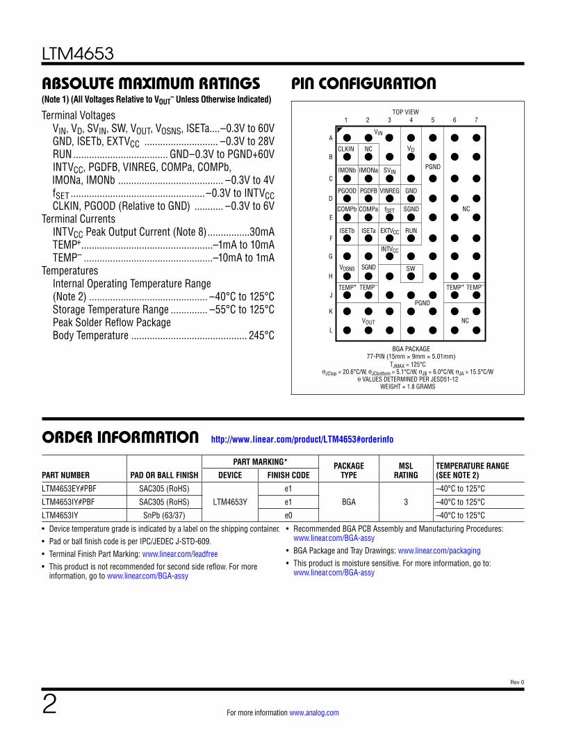
PIN CONFIGURATIONABSOLUTE MAXIMUM RATINGS
Terminal Voltages VIN, VD, SVIN, SW, VOUT, VOSNS, ISETa ....–0.3V to 60V GND, ISETb, EXTVCC ............................ –0.3V to 28V RUN .................................... GND–0.3V to PGND+60V INTVCC, PGDFB, VINREG, COMPa, COMPb, IMONa, IMONb ........................................ –0.3V to 4V fSET ...................................................–0.3V to INTVCC CLKIN, PGOOD (Relative to GND) ........... –0.3V to 6VTerminal Currents INTVCC Peak Output Current (Note 8) ................30mA TEMP+ ..................................................–1mA to 10mA TEMP– .................................................–10mA to 1mATemperatures Internal Operating Temperature Range
(Note 2) ............................................. –40°C to 125°C Storage Temperature Range .............. –55°C to 125°C Peak Solder Reflow Package
Body Temperature ............................................ 245°C
(Note 1) (All Voltages Relative to VOUT– Unless Otherwise Indicated)
1
A
B
C
D
E
F
G
H
J
K
L
2 3 4TOP VIEW
BGA PACKAGE77-PIN (15mm × 9mm × 5.01mm)
5 6 7
VIN
VD
VOUT
TEMP–
NC
NC
IMONa
NC
SW
GND
SVIN
VINREG
SGNDfSET
RUN
PGOOD PGDFB
CLKIN
PGND
PGND
SGNDVOSNS
EXTVCC
INTVCC
COMPb COMPa
ISETb ISETa
TEMP+TEMP–TEMP+
IMONb
TJMAX = 125°CθJCtop = 20.6°C/W, θJCbottom = 5.1°C/W, θJB = 6.0°C/W, θJA = 15.5°C/W
θ VALUES DETERMINED PER JESD51-12WEIGHT = 1.8 GRAMS
ORDER INFORMATION
PART NUMBER PAD OR BALL FINISH
PART MARKING* PACKAGE TYPE
MSL RATING
TEMPERATURE RANGE (SEE NOTE 2)DEVICE FINISH CODE
LTM4653EY#PBF SAC305 (RoHS)
LTM4653Y
e1
BGA 3
–40°C to 125°C
LTM4653IY#PBF SAC305 (RoHS) e1 –40°C to 125°C
LTM4653IY SnPb (63/37) e0 –40°C to 125°C
• Device temperature grade is indicated by a label on the shipping container.• Pad or ball finish code is per IPC/JEDEC J-STD-609.• Terminal Finish Part Marking: www.linear.com/leadfree• This product is not recommended for second side reflow. For more
information, go to www.linear.com/BGA-assy
• Recommended BGA PCB Assembly and Manufacturing Procedures: www.linear.com/BGA-assy
• BGA Package and Tray Drawings: www.linear.com/packaging• This product is moisture sensitive. For more information, go to:
www.linear.com/BGA-assy
http://www.linear.com/product/LTM4653#orderinfo
LTM4653
3Rev 0
For more information www.analog.com
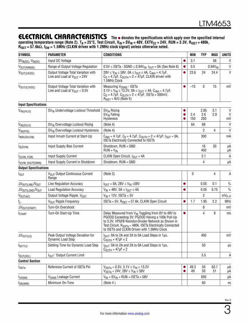
The l denotes the specifications which apply over the specified internal operating temperature range (Note 2). TA = 25°C, Test Circuit, VIN = SVIN = 48V, EXTVCC = 24V, RUN = 3.3V, RISET = 480k, RfSET = 57.6kΩ, fSW = 1.5MHz (CLKIN driven with 1.2MHz clock signal) unless otherwise noted.
SYMBOL PARAMETER CONDITIONS MIN TYP MAX UNITS
SVIN(DC), VIN(DC) Input DC Voltage l 3.1 58 V
VOUT(RANGE) Range of Output Voltage Regulation 0.5V ≤ ISETa - SGND ≤ 0.94VIN, IOUT = 0A (See Note 6) l 0.5 0.94VIN V
VOUT(24VDC) Output Voltage Total Variation with Line and Load at VOUT = 24V
28V ≤ VIN ≤ 58V, 0A ≤ IOUT ≤ 4A, CINH = 4.7μF, CD = 4.7μF, COUTH = 2 × 47μF, CLKIN driven with 1.5MHz Clock
l 23.6 24 24.4 V
VOUT(0.5VDC) Output Voltage Total Variation with Line and Load at VOUT = 0.5V
Measuring VOSNS - ISETa 3.1V ≤ VIN ≤ 13.2V, 0A ≤ IOUT ≤ 4A, CINH = 4.7μF, CD = 4.7μF, COUTH = 2 × 47μF, ISETa = 500mV, RfSET = N/U (Note 5)
l –15 0 15 mV
Input Specifications
VIN(UVLO) SVIN Undervoltage Lockout Threshold SVIN Rising SVIN Falling Hysteresis
l
l
l
2.4 150
2.85 2.6 250
3.1 2.9
V V
mV
VIN(OVLO) SVIN Overvoltage Lockout Rising (Note 4) 64 68 V
VIN(HYS) SVIN Overvoltage Lockout Hysteresis (Note 4) 2 4 V
IINRUSH(VIN) Input Inrush Current at Start-Up CINH = 4.7μF, CD = 4.7μF, COUTH = 2 × 47μF; IOUT = 0A, ISETa Electrically Connected to ISETb
300 mA
IQ(SVIN) Input Supply Bias Current Shutdown, RUN = GND RUN = VIN
16 450
30 μA μA
IS(VIN, FCM) Input Supply Current CLKIN Open Circuit, IOUT = 4A 2.1 A
IS(VIN, SHUTDOWN) Input Supply Current in Shutdown Shutdown, RUN = GND 4 µA
Output Specifications
IOUT VOUT Output Continuous Current Range
(Note 3) 0 4 A
∆VOUT(LINE)/VOUT Line Regulation Accuracy IOUT = 0A, 28V ≤ VIN ≤58V l 0.05 0.1 %
∆VOUT(LOAD)/VOUT Load Regulation Accuracy VIN = 48V, 0A ≤ IOUT ≤ 4A l 0.05 0.75 %
VOUT(AC) Output Voltage Ripple, VOUT VIN = 12V, ISETa = 5V 2 mVP–P
fs VOUT Ripple Frequency ISETa = 5V, RfSET = 57.6k, CLKIN Open Circuit l 1.7 1.95 2.2 MHz
∆VOUT(START) Turn-On Overshoot 8 mV
tSTART Turn-On Start-Up Time Delay Measured from VIN Toggling from 0V to 48V to PGOOD Exceeding 3V; PGOOD Having a 100k Pull-Up to 3.3V, VPGFB Resistor-Divider Network as Shown in Test Circuit, RISETa = 480k, ISETa Electrically Connected to ISETb and CLKIN Driven with 1.5MHz Clock
l 4 9 ms
∆VOUT(LS) Peak Output Voltage Deviation for Dynamic Load Step
IOUT: 0A to 2A and 2A to 0A Load Steps in 1μs, COUTH = 47µF × 2
400 mV
tSETTLE Settling Time for Dynamic Load Step IOUT: 0A to 2A and 2A to 0A Load Steps in 1μs, COUTH = 47µF × 2
50 µs
IOUT(OCL) IOUT– Output Current Limit 5.5 A
Control Section
IISETa Reference Current of ISETa Pin VISETa = 0.5V, 3.1V ≤ VIN ≤ 13.2V VISETa = 24V, 28V ≤ VIN ≤ 58V
l
l
49.3 49
50 50
50.7 51
µA µA
IVOSNS VOSNS Leakage Current VIN = SVIN = RUN = ISETa = 58V 600 µA
tON(MIN) Minimum On-Time (Note 4 ) 60 ns
ELECTRICAL CHARACTERISTICS
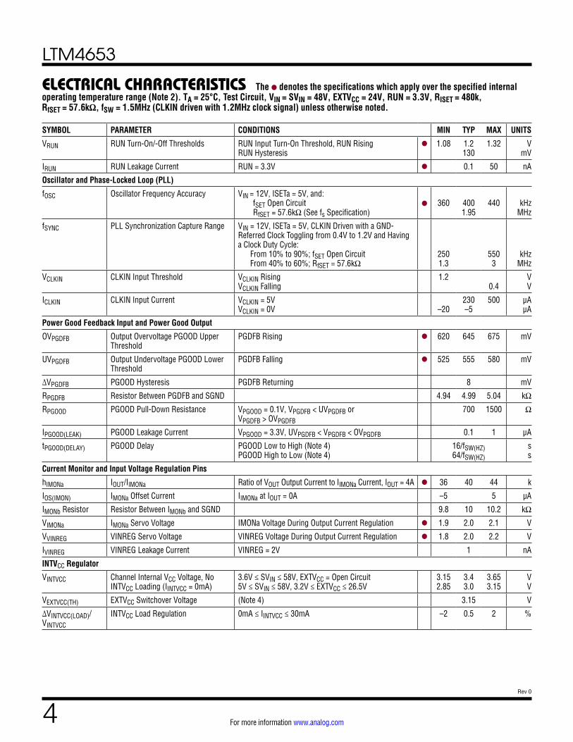
LTM4653
4Rev 0
For more information www.analog.com
The l denotes the specifications which apply over the specified internal operating temperature range (Note 2). TA = 25°C, Test Circuit, VIN = SVIN = 48V, EXTVCC = 24V, RUN = 3.3V, RISET = 480k, RfSET = 57.6kΩ, fSW = 1.5MHz (CLKIN driven with 1.2MHz clock signal) unless otherwise noted.
SYMBOL PARAMETER CONDITIONS MIN TYP MAX UNITS
VRUN RUN Turn-On/-Off Thresholds RUN Input Turn-On Threshold, RUN Rising RUN Hysteresis
l 1.08 1.2 130
1.32 V mV
IRUN RUN Leakage Current RUN = 3.3V l 0.1 50 nA
Oscillator and Phase-Locked Loop (PLL)
fOSC Oscillator Frequency Accuracy VIN = 12V, ISETa = 5V, and: fSET Open Circuit RfSET = 57.6kΩ (See fs Specification)
l
360
400 1.95
440
kHz
MHz
fSYNC PLL Synchronization Capture Range VIN = 12V, ISETa = 5V, CLKIN Driven with a GND-Referred Clock Toggling from 0.4V to 1.2V and Having a Clock Duty Cycle: From 10% to 90%; fSET Open Circuit From 40% to 60%; RfSET = 57.6kΩ
250 1.3
550 3
kHz MHz
VCLKIN CLKIN Input Threshold VCLKIN Rising VCLKIN Falling
1.2 0.4
V V
ICLKIN CLKIN Input Current VCLKIN = 5V VCLKIN = 0V
–20
230 –5
500 μA μA
Power Good Feedback Input and Power Good Output
OVPGDFB Output Overvoltage PGOOD Upper Threshold
PGDFB Rising l 620 645 675 mV
UVPGDFB Output Undervoltage PGOOD Lower Threshold
PGDFB Falling l 525 555 580 mV
∆VPGDFB PGOOD Hysteresis PGDFB Returning 8 mV
RPGDFB Resistor Between PGDFB and SGND 4.94 4.99 5.04 kΩ
RPGOOD PGOOD Pull-Down Resistance VPGOOD = 0.1V, VPGDFB < UVPGDFB or VPGDFB > OVPGDFB
700 1500 Ω
IPGOOD(LEAK) PGOOD Leakage Current VPGOOD = 3.3V, UVPGDFB < VPGDFB < OVPGDFB 0.1 1 μA
tPGOOD(DELAY) PGOOD Delay PGOOD Low to High (Note 4) PGOOD High to Low (Note 4)
16/fSW(HZ) 64/fSW(HZ)
s s
Current Monitor and Input Voltage Regulation Pins
hIMONa IOUT/IIMONa Ratio of VOUT Output Current to IIMONa Current, IOUT = 4A l 36 40 44 k
IOS(IMON) IMONa Offset Current IIMONa at IOUT = 0A –5 5 µA
IMONb Resistor Resistor Between IMONb and SGND 9.8 10 10.2 kΩ
VIMONa IMONa Servo Voltage IMONa Voltage During Output Current Regulation l 1.9 2.0 2.1 V
VVINREG VINREG Servo Voltage VINREG Voltage During Output Current Regulation l 1.8 2.0 2.2 V
IVINREG VINREG Leakage Current VINREG = 2V 1 nA
INTVCC Regulator
VINTVCC Channel Internal VCC Voltage, No INTVCC Loading (IINTVCC = 0mA)
3.6V ≤ SVIN ≤ 58V, EXTVCC = Open Circuit 5V ≤ SVIN ≤ 58V, 3.2V ≤ EXTVCC ≤ 26.5V
3.15 2.85
3.4 3.0
3.65 3.15
V V
VEXTVCC(TH) EXTVCC Switchover Voltage (Note 4) 3.15 V
∆VINTVCC(LOAD)/VINTVCC
INTVCC Load Regulation 0mA ≤ IINTVCC ≤ 30mA –2 0.5 2 %
ELECTRICAL CHARACTERISTICS
LTM4653
5Rev 0
For more information www.analog.com
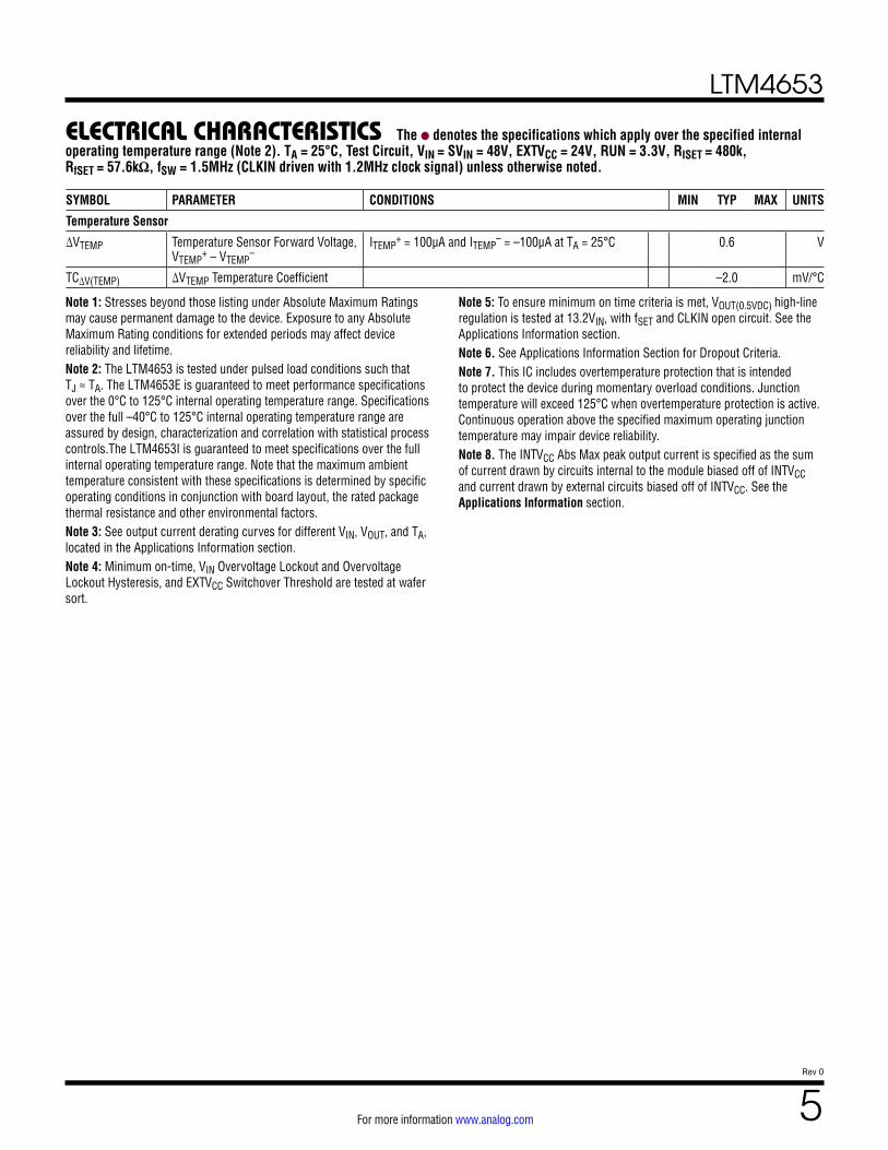
The l denotes the specifications which apply over the specified internal operating temperature range (Note 2). TA = 25°C, Test Circuit, VIN = SVIN = 48V, EXTVCC = 24V, RUN = 3.3V, RISET = 480k, RfSET = 57.6kΩ, fSW = 1.5MHz (CLKIN driven with 1.2MHz clock signal) unless otherwise noted.
Note 1: Stresses beyond those listing under Absolute Maximum Ratings may cause permanent damage to the device. Exposure to any Absolute Maximum Rating conditions for extended periods may affect device reliability and lifetime.Note 2: The LTM4653 is tested under pulsed load conditions such that TJ ≈ TA. The LTM4653E is guaranteed to meet performance specifications over the 0°C to 125°C internal operating temperature range. Specifications over the full –40°C to 125°C internal operating temperature range are assured by design, characterization and correlation with statistical process controls.The LTM4653I is guaranteed to meet specifications over the full internal operating temperature range. Note that the maximum ambient temperature consistent with these specifications is determined by specific operating conditions in conjunction with board layout, the rated package thermal resistance and other environmental factors.Note 3: See output current derating curves for different VIN, VOUT, and TA, located in the Applications Information section.Note 4: Minimum on-time, VIN Overvoltage Lockout and Overvoltage Lockout Hysteresis, and EXTVCC Switchover Threshold are tested at wafer sort.
Note 5: To ensure minimum on time criteria is met, VOUT(0.5VDC) high-line regulation is tested at 13.2VIN, with fSET and CLKIN open circuit. See the Applications Information section.Note 6. See Applications Information Section for Dropout Criteria.Note 7. This IC includes overtemperature protection that is intended to protect the device during momentary overload conditions. Junction temperature will exceed 125°C when overtemperature protection is active. Continuous operation above the specified maximum operating junction temperature may impair device reliability.Note 8. The INTVCC Abs Max peak output current is specified as the sum of current drawn by circuits internal to the module biased off of INTVCC and current drawn by external circuits biased off of INTVCC. See the Applications Information section.
SYMBOL PARAMETER CONDITIONS MIN TYP MAX UNITS
Temperature Sensor
∆VTEMP Temperature Sensor Forward Voltage, VTEMP
+ – VTEMP–
ITEMP+ = 100µA and ITEMP
– = –100μA at TA = 25°C 0.6 V
TC∆V(TEMP) ∆VTEMP Temperature Coefficient –2.0 mV/°C
ELECTRICAL CHARACTERISTICS
LTM4653
6Rev 0
For more information www.analog.com
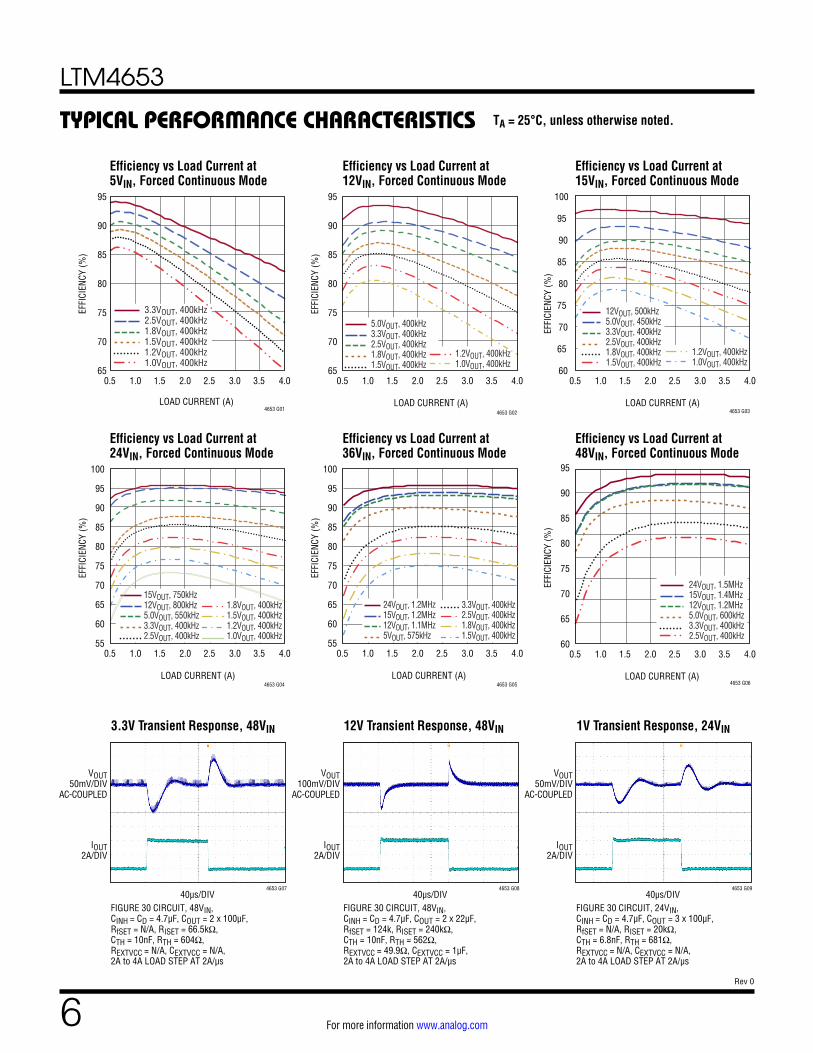
TYPICAL PERFORMANCE CHARACTERISTICS TA = 25°C, unless otherwise noted.
Efficiency vs Load Current at5VIN, Forced Continuous Mode
Efficiency vs Load Current at12VIN, Forced Continuous Mode
Efficiency vs Load Current at15VIN, Forced Continuous Mode
Efficiency vs Load Current at24VIN, Forced Continuous Mode
Efficiency vs Load Current at36VIN, Forced Continuous Mode
Efficiency vs Load Current at48VIN, Forced Continuous Mode
3.3V Transient Response, 48VIN 12V Transient Response, 48VIN 1V Transient Response, 24VIN
1.2VOUT, 400kHz1.5VOUT, 400kHz1.8VOUT, 400kHz2.5VOUT, 400kHz3.3VOUT, 400kHz
1.0VOUT, 400kHz65
70
75
80
85
90
95
0.5 1.0 1.5 2.0 2.5 3.0 3.5 4.0
EFFI
CIEN
CY (%
)
LOAD CURRENT (A) 4653 G01
1.5VOUT, 400kHz1.8VOUT, 400kHz2.5VOUT, 400kHz3.3VOUT, 400kHz5.0VOUT, 400kHz
1.2VOUT, 400kHz1.0VOUT, 400kHz
65
70
75
80
85
90
95
0.5 1.0 1.5 2.0 2.5 3.0 3.5 4.0
EFFI
CIEN
CY (%
)
LOAD CURRENT (A) 4653 G02
1.8VOUT, 400kHz2.5VOUT, 400kHz3.3VOUT, 400kHz5.0VOUT, 450kHz12VOUT, 500kHz
1.5VOUT, 400kHz1.2VOUT, 400kHz1.0VOUT, 400kHz
60
65
70
75
80
85
90
95
100
0.5 1.0 1.5 2.0 2.5 3.0 3.5 4.0
EFFI
CIEN
CY (%
)
LOAD CURRENT (A) 4653 G03
2.5VOUT, 400kHz3.3VOUT, 400kHz5.0VOUT, 550kHz12VOUT, 800kHz15VOUT, 750kHz
1.0VOUT, 400kHz1.2VOUT, 400kHz1.5VOUT, 400kHz1.8VOUT, 400kHz
55
60
65
70
75
80
85
90
95
100
0.5 1.0 1.5 2.0 2.5 3.0 3.5 4.0
EFFI
CIEN
CY (%
)
LOAD CURRENT (A) 4653 G04
5VOUT, 575kHz12VOUT, 1.1MHz15VOUT, 1.2MHz24VOUT, 1.2MHz
1.5VOUT, 400kHz1.8VOUT, 400kHz2.5VOUT, 400kHz
55
60
65
70
75
80
85
90
95
100
0.5 1.0 1.5 2.0 2.5 3.0 3.5 4.0
EFFI
CIEN
CY (%
)
LOAD CURRENT (A) 4653 G05
3.3VOUT, 400kHz
3.3VOUT, 400kHz5.0VOUT, 600kHz12VOUT, 1.2MHz15VOUT, 1.4MHz24VOUT, 1.5MHz
2.5VOUT, 400kHz60
65
70
75
80
85
90
95
0.5 1.0 1.5 2.0 2.5 3.0 3.5 4.0
EFFI
CIEN
CY (%
)
LOAD CURRENT (A) 4653 G06
40µs/DIV
VOUT50mV/DIV
AC-COUPLED
IOUT2A/DIV
4653 G07
FIGURE 30 CIRCUIT, 48VIN,CINH = CD = 4.7µF, COUT = 2 x 100µF,RfSET = N/A, RISET = 66.5kΩ,CTH = 10nF, RTH = 604Ω,REXTVCC = N/A, CEXTVCC = N/A,2A to 4A LOAD STEP AT 2A/µs
40µs/DIV
VOUT100mV/DIV
AC-COUPLED
IOUT2A/DIV
4653 G08
FIGURE 30 CIRCUIT, 48VIN,CINH = CD = 4.7µF, COUT = 2 x 22µF,RfSET = 124k, RISET = 240kΩ,CTH = 10nF, RTH = 562Ω,REXTVCC = 49.9Ω, CEXTVCC = 1µF,2A to 4A LOAD STEP AT 2A/µs
40µs/DIV
VOUT50mV/DIV
AC-COUPLED
IOUT2A/DIV
4653 G09
FIGURE 30 CIRCUIT, 24VIN,CINH = CD = 4.7µF, COUT = 3 x 100µF,RfSET = N/A, RISET = 20kΩ,CTH = 6.8nF, RTH = 681Ω,REXTVCC = N/A, CEXTVCC = N/A,2A to 4A LOAD STEP AT 2A/µs
LTM4653
7Rev 0
For more information www.analog.com
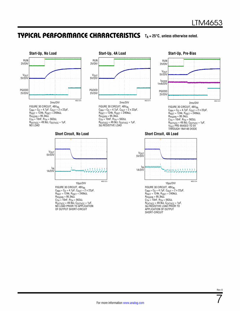
TYPICAL PERFORMANCE CHARACTERISTICS TA = 25°C, unless otherwise noted.
Start-Up, No Load Start-Up, 4A Load Start-Up, Pre-Bias
Short Circuit, No Load Short Circuit, 4A Load
2ms/DIV
RUN2V/DIV
PGOOD2V/DIV
VOUT5V/DIV
4653 G10
FIGURE 30 CIRCUIT, 48VIN,CINH = CD = 4.7µF, COUT = 2 x 22µF,RfSET = 124k, RISET = 240kΩ,RPGDFB = 95.3kΩ,CTH = 10nF, RTH = 562Ω,REXTVCC = 49.9Ω, CEXTVCC = 1µF,NO LOAD
2ms/DIV
RUN2V/DIV
PGOOD2V/DIV
VOUT5V/DIV
4653 G11
FIGURE 30 CIRCUIT, 48VIN,CINH = CD = 4.7µF, COUT = 2 x 22µF,RfSET = 124k, RISET = 240kΩ,RPGDFB = 95.3kΩ,CTH = 10nF, RTH = 562Ω,REXTVCC = 49.9Ω, CEXTVCC = 1µF,3Ω RESISTIVE LOAD
2ms/DIV
RUN2V/DIV
PGOOD2V/DIV
VOUT5V/DIV
IDIODE1mA/DIV
4653 G12
FIGURE 30 CIRCUIT, 48VIN,CINH = CD = 4.7µF, COUT = 2 x 22µF,RfSET = 124k, RISET = 240kΩ,RPGDFB = 95.3kΩ,CTH = 10nF, RTH = 562Ω,REXTVCC = 49.9Ω, CEXTVCC = 1µF,VOUT PRE-BIASED TO 5VTHROUGH 1N4148 DIODE
10µs/DIV
VOUT5V/DIV
IIN1A/DIV
4653 G13
FIGURE 30 CIRCUIT, 48VIN,CINH = CD = 4.7µF, COUT = 2 x 22µF,RfSET = 124k, RISET = 240kΩ,RPGDFB = 95.3kΩ,CTH = 10nF, RTH = 562Ω,REXTVCC = 49.9Ω, CEXTVCC = 1µF,NO LOAD PRIOR TO APPLICATIONOF OUTPUT SHORT-CIRCUIT
10µs/DIV
VOUT5V/DIV
IIN1A/DIV
4653 G14
FIGURE 30 CIRCUIT, 48VIN,CINH = CD = 4.7µF, COUT = 2 x 22µF,RfSET = 124k, RISET = 240kΩ,RPGDFB = 95.3kΩ,CTH = 10nF, RTH = 562Ω,REXTVCC = 49.9Ω, CEXTVCC = 1µF,3Ω RESISTIVE LOAD PRIOR TOAPPLICATION OF OUTPUTSHORT-CIRCUIT
LTM4653
8Rev 0
For more information www.analog.com
PIN FUNCTIONS
VIN (A1-A3, B3): Power Input Pins. Apply input voltage and input decoupling capacitance directly between VIN and a ground (PGND) plane.
VD (A4, B4, C4): Drain of the Converter’s Primary Switch-ing MOSFET. Apply at minimum one 4.7µF high frequency ceramic decoupling capacitor directly from VD to PGND. Give this capacitor higher layout priority (closer proximity to the module) than any VIN decoupling capacitors.
SVIN (C3): Input Voltage Supply for Small-Signal Circuits. SVIN is the input to the INTVCC LDO. Connect SVIN directly to VIN. No decoupling capacitor is needed on this pin.
PGND (A5, B5, C5, D5, E5, F5, G4-5, H3, H5, J3-5, K4-5, L4-5): Power Ground Pins of the LTM4653. Connect all pins to the application’s PGND plane.
VOUT (K1-3, L1-3): Power Output Pins of the LTM4653. Connect all pins to the application’s power VOUT plane. Apply the output filter capacitors and the output load between a power VOUT plane and the application’s PGND plane.
GND (D4): Ground Pin of the LTM4653. Electrically con-nect to the application’s PGND plane.
VOSNS (G1, H1): Output Voltage Sense and Feedback Signal. Connect VOSNS to VOUT at the point of load (POL). Pins G1 and H1 are electrically connected to each other internal to the module, and thus it is only necessary to connect one VOSNS pin to VOUT at the POL. The remaining VOSNS pin can be used for redundant connectivity or routed to an ICT test point for design-for-test considerations, as desired.
SGND (E4, G2, H2): Signal Ground Pins of the LTM4653. Connect Pin H2 to PGND directly under the LTM4653. The SGND pins at locations E4 and G2 are electrically con-nected to each other internal to the module, and thus it is only necessary to connect one SGND pin to PGND under the module. The remaining SGND pins can be used for redundant connectivity or routed to an ICT test point for design-for-test considerations, as desired.
RUN (F4): Run Control Pin. A voltage above 1.2V com-mands the Module to regulate its output voltage. Under-voltage lockout (UVLO) can be implemented by connecting RUN to the midpoint node formed by a resistor-divider between VIN and GND. RUN features 130mV of hysteresis. See the Applications Information section.
INTVCC (G3): Internal Regulator, 3.3V Nominal Output. Internal control circuits and MOSFET-drivers derive pow-er from INTVCC bias. When operating 3.1V < SVIN ≤ 58V, an LDO generates INTVCC from SVIN when RUN is logic high (RUN > 1.2V). No external decoupling is required. When RUN is logic low (RUN - GND < 1.2V), the INTVCC LDO is off, i.e., INTVCC is unregulated. (Also see EXTVCC.)
EXTVCC (F3): External Bias, Auxiliary Input to the INTVCC Regulator. When EXTVCC exceeds 3.2V and SVIN exceeds 5V, the INTVCC LDO derives power from EXTVCC bias instead of the SVIN path. This technique can reduce LDO losses considerably, resulting in a corresponding reduc-tion in module junction temperature. For applications in which 4V ≤ VOUT ≤ 26.5V, connect EXTVCC to VOUT through a resistor. (See the Applications Information section for resistor value.) When taking advantage of this EXTVCC feature, locally decouple EXTVCC to PGND with a 1µF ce-ramic—otherwise, leave EXTVCC open circuit.
ISETb (F1): 1.5nF Soft-Start Capacitor. Connect ISETb to ISETa to achieve default soft-start characteristics, if desired. See ISETa.
ISETa (F2): Accurate 50μA Current Source. Positive input to the error amplifier. Connect a resistor (RISET) from this pin to SGND to program the desired LTM4653 output volt-age, VOUT = RISET • 50μA. A capacitor can be connected from ISETa to SGND to soft-start the output voltage and reduce start-up inrush current. Connect ISETa to ISETb in order to achieve default soft-start, if desired. (See ISETb.)
In addition, the output of the LTM4653 can track a voltage applied between the ISETa pin and the SGND pins. (See the Applications Information section.)
PACKAGE ROW AND COLUMN LABELING MAY VARY AMONG µModule PRODUCTS. REVIEW EACH PACKAGE LAYOUT CAREFULLY.
LTM4653
9Rev 0
For more information www.analog.com
PGOOD (D1): Power Good Indicator, Open-Drain Output Pin. PGOOD is high impedance when PGDFB is within approximately ±7.5% of 0.6V. PGOOD is pulled to GND when PGDFB is outside this range.
PGDFB (D2): Power Good Feedback Programming Pin. Connect PGDFB to VOSNS through a resistor, RPGDFB. RPGDFB configures the voltage threshold of VOUT for which PGOOD toggles its state. If the PGOOD feature is used, set RPGDFB to:
RPGDFB =
VOUT0.6V
– 1⎛
⎝⎜
⎞
⎠⎟ • 4.99k
otherwise, leave PGDFB open circuit.
A small filter capacitor (220pF) internal to the LTM4653 on this pin provides high frequency noise immunity for the PGOOD output indicator.
fSET (E3): Oscillator Frequency Programming Pin. The default switching frequency of the LTM4653 is 400kHz. Often, it is necessary to increase the programmed fre-quency by connecting a resistor between fSET and SGND. (See the Applications Information section.) Note that the synchronization range of CLKIN is approximately ±40% of the oscillator frequency programmed by the fSET pin.
CLKIN (B1): Mode Select and Oscillator Synchronization Input. Leave CLKIN open circuit for forced continuous mode operation. Alternatively, this pin can be driven to synchronize the switching frequency of the LTM4653 to a clock signal. In this condition, the LTM4653 operates in forced continuous mode and the cycle-by-cycle turn-on of the primary power MOSFET MT is coincident with the rising edge of the clock applied to CLKIN. Note the synchronization range of CLKIN is approximately ±40% of the oscillator frequency programmed by the fSET pin. (See the Applications Information section.)
COMPa (E2): Current Control Threshold and Error Ampli-fier Compensation Node. The trip threshold of LTM4653’s current comparator increases with a corresponding rise in COMPa voltage. A small filter cap (10pF) internal to the LTM4653 on this pin introduces a high-frequency roll-off of the error-amplifier response, yielding good noise rejection in the control-loop. COMPa is often electrically connected to COMPb in one’s application, thus applying
default loop compensation. Loop compensation (a series resistor-capacitor) can be applied externally to COMPa if desired or needed, instead. (See COMPb.)
COMPb (E1): Internal Loop Compensation Network. For most applications, the internal, default loop compensation of the LTM4653 is suitable to apply “as is”, and yields very satisfactory results: apply the default loop compensation to the control loop by simply connecting COMPa to COMPb. When more specialized applications require a personal touch to the optimization of control loop response, this can be accomplished by connecting a series resistor-capacitor network from COMPa to SGND—and leaving COMPb open circuit.
VINREG (D3): Input Voltage Regulation Programming Pin. Optionally connect this pin to the midpoint node formed by a resistor-divider between VD and SGND. When the voltage on VINREG falls below approximately 2V, a VINREG control loop servos VOUT to decrease the power inductor current and thus regulate VINREG at 2V. (See the Applications Information section.)
If this input voltage regulation feature is not desired, con-nect VINREG to INTVCC.
IMONa (C2): Power Inductor Current Analog Indicator Pin and Current Limit Programming Pin. The current flowing out of this pin is equal to 1/40,000 of the average power inductor current. To construct a voltage (VIMONa) that is proportional to the power inductor current, optionally apply a parallel resistor-capacitor network to this pin and terminate it to SGND.
IMONa can be connected to IMONb if the default resis-tor-capacitor termination network provided by IMONb is desired: 1V at full scale (4A) load current. (See IMONb.) If this analog indicator feature is not desired, connect IMONa to SGND.
If IMONa ever exceeds a trip threshold of approximately 2V, an IMON control loop servos VOUT to decrease power inductor current and thus regulate IMONa at 2V. In this manner, the average current limit inception threshold of the LTM4653 can be configured. (See the Applications Information section.)
PIN FUNCTIONS
LTM4653
10Rev 0
For more information www.analog.com
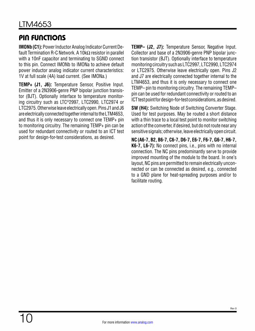
IMONb (C1): Power Inductor Analog Indicator Current De-fault Termination R-C Network. A 10kΩ resistor in parallel with a 10nF capacitor and terminating to SGND connect to this pin. Connect IMONb to IMONa to achieve default power inductor analog indicator current characteristics: 1V at full scale (4A) load current. (See IMONa.)
TEMP+ (J1, J6): Temperature Sensor, Positive Input. Emitter of a 2N3906-genre PNP bipolar junction transis-tor (BJT). Optionally interface to temperature monitor-ing circuitry such as LTC®2997, LTC2990, LTC2974 or LTC2975. Otherwise leave electrically open. Pins J1 and J6 are electrically connected together internal to the LTM4653, and thus it is only necessary to connect one TEMP+ pin to monitoring circuitry. The remaining TEMP+ pin can be used for redundant connectivity or routed to an ICT test point for design-for-test considerations, as desired.
TEMP– (J2, J7): Temperature Sensor, Negative Input. Collector and base of a 2N3906-genre PNP bipolar junc-tion transistor (BJT). Optionally interface to temperature monitoring circuitry such as LTC2997, LTC2990, LTC2974 or LTC2975. Otherwise leave electrically open. Pins J2 and J7 are electrically connected together internal to the LTM4653, and thus it is only necessary to connect one TEMP– pin to monitoring circuitry. The remaining TEMP– pin can be used for redundant connectivity or routed to an ICT test point for design-for-test considerations, as desired.
SW (H4): Switching Node of Switching Converter Stage. Used for test purposes. May be routed a short distance with a thin trace to a local test point to monitor switching action of the converter, if desired, but do not route near any sensitive signals; otherwise, leave electrically open circuit.
NC (A6-7, B2, B6-7, C6-7, D6-7, E6-7, F6-7, G6-7, H6-7, K6-7, L6-7): No connect pins, i.e., pins with no internal connection. The NC pins predominantly serve to provide improved mounting of the module to the board. In one’s layout, NC pins are permitted to remain electrically uncon-nected or can be connected as desired, e.g., connected to a GND plane for heat-spreading purposes and/or to facilitate routing.
PIN FUNCTIONS
LTM4653
11Rev 0
For more information www.analog.com
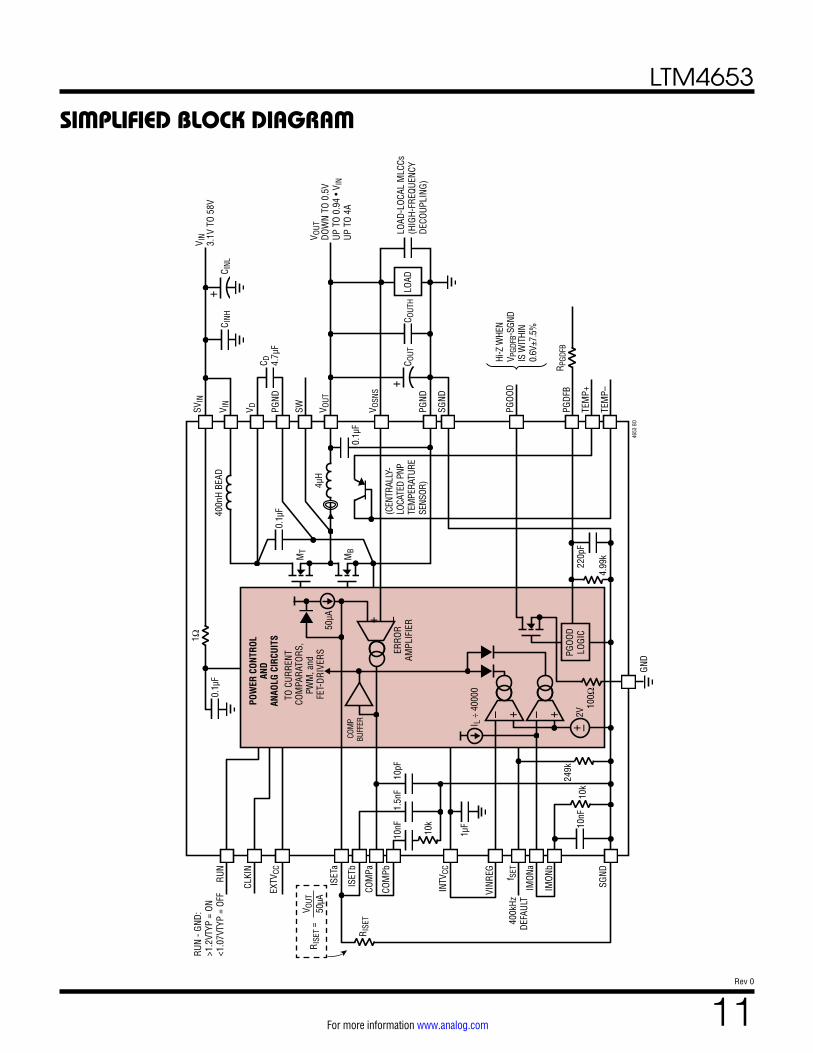
SIMPLIFIED BLOCK DIAGRAM
+
+
V IN
3.1V
TO
58V
V OUT
DOW
N TO
0.5
VUP
TO
0.94
• V I
NUP
TO
4A
LOAD
-LOC
AL M
LCCs
(HIG
H-FR
EQUE
NCY
DECO
UPLI
NG)
C D 4.7µ
F
SVIN
V IN
V D V OUT
V OSN
S
I L ÷
400
00
C OUT
HC O
UT
MT
MB
PGND
PGND
PGOO
D
(CEN
TRAL
LY-
LOCA
TED
PNP
TEM
PERA
TURE
SENS
OR)
SGND
GND
SGND
IMON
b
400k
HzDE
FAUL
TIM
ONa
VINR
EG
COM
Pb
COM
Pa
ISET
a
EXTV
CC
RUN
CLKI
N
RUN
- GND
:>1
.2VT
YP =
ON
<1.0
7VTY
P =
OFF
ISET
b
10k
10nF
1.5n
F10
pF
50µA
1µF
INTV
CC
R ISE
T
R ISE
T =
PGDF
B
4.99
k10
0Ω
249k
10k
10nF
2V22
0pF
4653
BD
TEM
P+
TEM
P–
SW
0.1µ
F
ERRO
RAM
PLIF
IER
TO C
URRE
NT
COM
PARA
TORS
,PW
M, a
nd
FET-
DRIV
ERS
POW
ER C
ONTR
OLAN
DAN
AOLG
CIR
CUIT
S
0.1µ
F
1Ω
4µH
0.1µ
F
400n
H BE
ADC I
NLC I
NH
LOAD
Hi-Z
WHE
NV P
GDFB
-SGN
DIS
WIT
HIN
0.6V
±7.5
%
R PGD
FB
+ –
+–+–
+ –
f SET
V OUT
50µA
COM
P BU
FFER
PGOO
DLO
GIC
LTM4653
12Rev 0
For more information www.analog.com
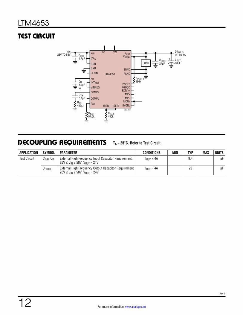
TEST CIRCUIT
DECOUPLING REQUIREMENTSAPPLICATION SYMBOL PARAMETER CONDITIONS MIN TYP MAX UNITS
Test Circuit CINH, CD External High Frequency Input Capacitor Requirement, 28V ≤ VIN ≤ 58V, VOUT
= 24VIOUT = 4A 9.4 µF
COUTH External High Frequency Output Capacitor Requirement 28V ≤ VIN ≤ 58V, VOUT = 24V
IOUT = 4A 22 µF
TA = 25°C. Refer to Test Circuit
VIN
SVIN
RUN
GND
CLKIN
VOUTVOSNS
PGND
PGOOD
IMONaIMONbISETbISETa
TEMP+TEMP–
EXTVCC
PGDFB
24VOUT,UP TO 4A
COUTL68µF
COUTH27µF
SGND
RPGDFB196k
RISET480k
RfSET57.6k
RTH499Ω
CD4.7μFx2
CINH4.7μF
CTH0.1μF
VDINTVCC
VINREG
4653 TC01
NC SW
LTM4653
COMPa
COMPb
fSET
VIN28V TO 58V
+LOAD
LTM4653
13Rev 0
For more information www.analog.com
Power Module Description
The LTM4653 is a non-isolated switch mode DC/DC step-down power supply. It can provide up to 4A output current with a few external input and output capacitors. Set by a single resistor, RISET, the LTM4653 regulates a positive output voltage, VOUT. VOUT can be set to as low as 0.5V to as high as 0.94VIN. The LTM4653 operates from a positive input supply rail, VIN, between 3.1V and 58V. The typical application schematic is shown in Figure 30.
The LTM4653 contains an integrated constant-frequency current mode regulator, power MOSFETs, power inductor, EMI filter and other supporting discrete components. The nominal switching frequency range is from 400kHz to 3MHz, and the default operating frequency is 400kHz. It can be externally synchronized to a clock, from 250kHz to 3MHz. See the Applications Information section. The LTM4653 supports internal and external control loop compensation. Internal loop compensation is selected by connecting the COMPa and COMPb pins. Using internal loop compensation, the LTM4653 has sufficient stability margins and good transient performance with a wide range of output capacitors—even ceramic-only output capacitors. For external loop compensation, see the Applications Information section. LTpowerCAD® is available for transient load step and stability analysis. Input filter and noise cancellation circuitry reduces noise-coupling to the module’s inputs and outputs, ensuring the module’s electromagnetic interference (EMI) meets the limits of EN55022 Class B (see Figures 4 to 6).
Pulling the RUN pin below 1.2V forces the LTM4653 into a shutdown state. A capacitor can be applied from ISETa to SGND to program the output voltage ramp-rate; or, the default LTM4653 ramp-rate can be set by connecting ISETa to ISETb; or, voltage tracking can be implemented by interfacing rail voltages to the ISETa pin. See the Applications Information section.
Multiphase operation can be employed by applying an external clock source to the LTM4653’s synchronization input, the CLKIN pin. See the Typical Applications section.
LDO losses within the module are reduced by connecting EXTVCC to VOUT through an RC-filter or by connecting EXTVCC to a suitable voltage source.
OPERATIONIMONa is an analog output current indicator pin. It sources a current proportional to the LTM4653’s load current. When IMONa is electrically connected to IMONb, the voltage on the IMONa/IMONb node is proportional to load current—with 1V corresponding to 4A load. IMONa can be interfaced to an external parallel-RC network instead of the one provided by IMONb. If IMONa ever exceeds 2V, a servo loop reduces the LTM4653’s output current in order to keep IMONa at or below 2V. Through this servo mechanism, a parallel RC network can be connected to IMONa to implement an average current limit function—if desired. When the feature is not needed, connect IMONa to SGND.
The LTM4653 also features a spare control pin called VINREG, with a 2V servo threshold, which can be used to reduce the input current draw during input line sag (“brownout”) conditions. Connect VINREG to INTVCC when this feature is not needed.
TEMP+ and TEMP– pins give access to a diode-con-nected PNP transistor, making it possible to monitor the LTM4653’s internal temperature—if desired.
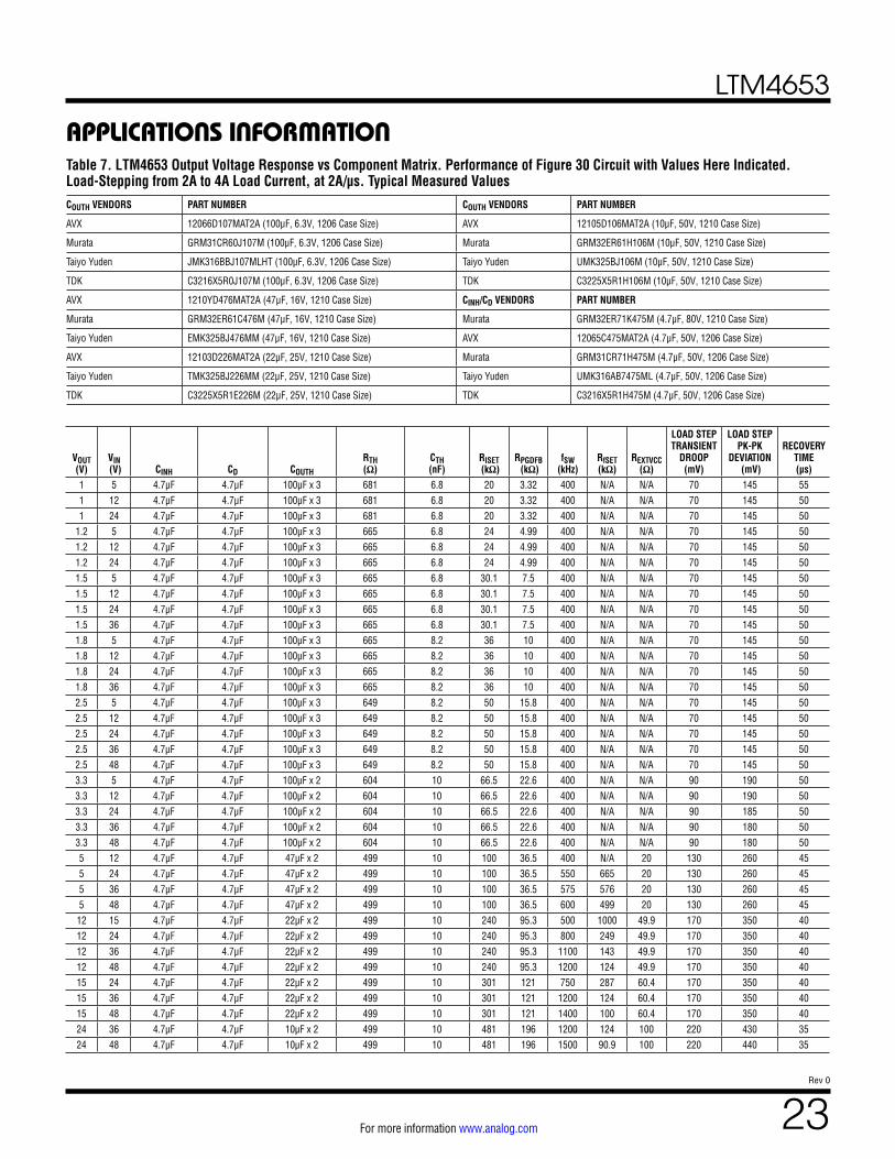
External component selection is primarily determined by the maximum load current and output voltage. Refer to Table 7 and the Test Circuit for recommended external component values.
VIN to VOUT Step-Down Ratios
There are restrictions on the VIN to VOUT step-down ratio that the LTM4653 can achieve. The maximum duty cycle of the LTM4653 is 96% typical. The VIN to VOUT mini-mum dropout voltage is a function of load current when operating in high duty cycle applications. As an example, VOUT(24VDC) from the Electrical Characteristics table high-lights the LTM4653’s ability to regulate 24VOUT at up to 4A from 28VIN, when running at a switching frequency, fSW, of 1.5MHz.
At very low duty cycles, the LTM4653’s on-time of MT each switching cycle should be designed to exceed the LTM4653 control loop’s specified minimum on-time of 60ns, tON(MIN), (guardband to 90ns), i.e.:
DfSW
> TON(MIN)
LTM4653
14Rev 0
For more information www.analog.com
where D (unitless) is the duty-cycle of MT, given by:
D =VOUTVIN
In rare cases where the minimum on-time restriction is violated, the frequency of the LTM4653 automatically and gradually folds back down to approximately one-fifth of its programmed switching frequency to allow VOUT to remain in regulation. See the Frequency Adjustment section. Be reminded of Notes 2, 3 and 5 in the Electrical Characteristics section regarding output current guidelines.
Input Capacitors
The LTM4653 achieves low input conducted EMI noise due to tight layout and high-frequency bypassing of MOSFETs MT and MB within the module itself. A small filter inductor (400nH) is integrated in the input line (from VIN to VD), providing further noise attenuation—again, local to the switching MOSFETs. The VD and VIN pins are available for external input capacitors—CD and CINH—to form a high-frequency π filter. As shown in the Simplified Block Diagram, the ceramic capacitor CD on the LTM4653’s VD pins handles the majority of the RMS current into the DC/DC converter power stage and requires careful selection, for that reason.
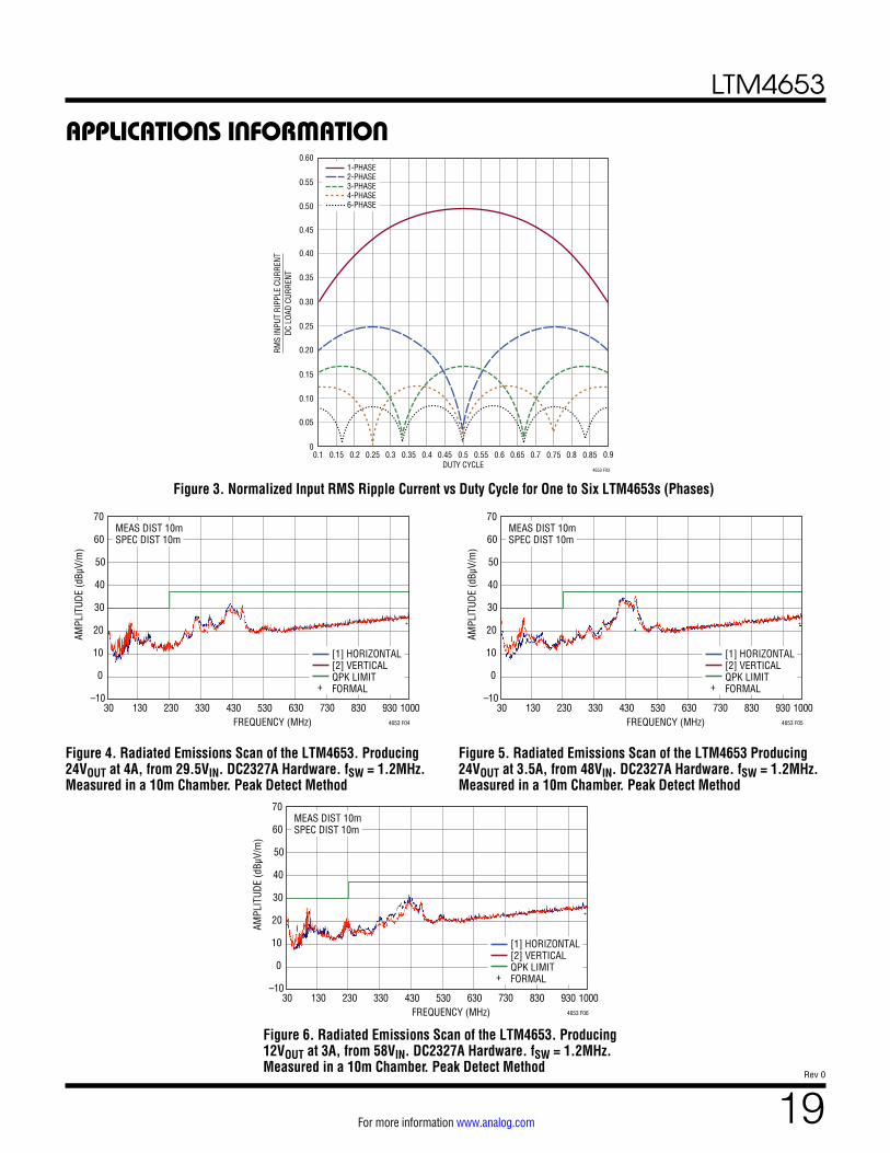
See Figures 4 to 6 for demonstration of LTM4653’s EMI performance, meeting the radiated emissions requirements of EN55022B.
The input capacitance, CD, is needed to filter the pulsed current drawn by MT. To prevent excessive voltage sag on VD, a low-effective series resistance (low-ESR, such as an X7R ceramic) input capacitor should be used, sized appropriately for the maximum CD RMS ripple current:
ICD(RMS) =
IOUT(MAX)
η%• D • (1– D)
where η% is the estimated efficiency of the power module. (See Typical Performance Characteristics graphs.)
Several capacitors may be paralleled to meet the applica-tion’s target size, height, and CD RMS ripple current rating. For lower input voltage applications, sufficient bulk input capacitance is needed to counteract line sag and transient
OPERATIONeffects during output load changes. The bulk capacitor can be a switcher-rated aluminum electrolytic capacitor or a Polymer capacitor. Suggested values for CD and CINH are found in Table 7.
A final precaution regarding ceramic capacitors concerns the maximum input voltage rating of the LTM4653’s VIN, SVIN, and VD pins. A ceramic input capacitor combined with trace or cable inductance forms a high Q (underdamped) tank circuit. If the LTM4653 circuit is plugged into a live supply, the input voltage can ring to twice its nominal value, possibly exceeding the device’s rating. This situa-tion is easily avoided; see the Hot-Plugging Safely section.
Output Capacitors
Output capacitors COUTH and COUTL are applied to VOUT of the LTM4653. Sufficient capacitance and low ESR are called for, to meet the output voltage ripple, loop stability, and transient requirements. COUTL can be a low ESR tantalum or polymer capacitor. COUTH is a ceramic capacitor. The typical output capacitance is 22μF (type X5R material, or better), if ceramic-only output capacitors are used.
Table 7 shows a matrix of suggested output capacitors optimized for 2A transient step-loads applied at 2A/μs. Additional output filtering may be required by the system designer, if further reduction of output ripple or dynamic transient spike is required. The LTpowerCAD design tool is available for transient and stability analysis. Stability criteria are considered in the Table 7 matrix, and LTpowerCAD is available for stability analysis. Multiphase operation will reduce effective output ripple as a function of the num-ber of phases. Application Note 77 discusses this noise reduction versus output ripple current cancellation, but the output capacitance should be considered carefully as a function of stability and transient response. LTpowerCAD can be used to calculate the output ripple reduction as the number of implemented phases increases by N times. External loop compensation can be applied to COMPa if needed, for transient response optimization.
Forced Continuous Operation
Leave the CLKIN pin open circuit to command the LTM4653 for forced continuous operation. In this mode, the control loop is allowed to command the inductor peak current to
LTM4653
15Rev 0
For more information www.analog.com
OPERATIONapproximately –1A, allowing for significant negative aver-age current. Clocking the CLKIN pin at a frequency within ±40% of the target switching frequency commanded by the fSET pin synchronizes MT’s turn-on to the rising edge of the CLKIN pin.
Output Voltage Programming, Tracking and Soft-Start
The LTM4653 regulates its output voltage, VOUT, accord-ing to the differential voltage present across ISETa and SGND. In most applications, the output voltage is set by simply connecting a resistor, RISET, from ISETa to SGND, according to:
RISET =VOUT
50µA
Since the LTM4653 control loop servos its output volt-age according to the voltage between ISETa and SGND: placing a capacitor, CSS, parallel to RSET configures the ramp-up rate of ISETa and thus VOUT. In the time domain, the output voltage ramp-up after the RUN pin is toggled from low to high (t = 0s) is given by:
VOUT(t) = IISETa •RISET • 1– e–
tRISET • CSS
⎛
⎝
⎜⎜⎜
⎞
⎠
⎟⎟⎟
The soft-start time, tSS, is defined as the time it takes for VOUT to ramp from 0V to 90% of its final value:
tSS = –RISET • CSS •In (1– 0.9) or
tSS = 2.3 • RISET • CSS
A default value of CSS = 1.5nF can be implemented by connecting ISETa to ISETb. For other ramp-up rates, connect an external CSS capacitor parallel to RISET. When starting up into a pre-biased VOUT, the LTM4653 stays in a sleep mode, keeping MT and MB off until VISETa equals VOSNS—after which, the DC/DC converter commences switching action and VOUT is ramped according to the voltage commanded by ISETa.
Since the LTM4653 control loop servos its VOSNS voltage to match that of ISETa’s, the LTM4653’s output can be configured to track any voltage applied to ISETa, refer-enced to SGND.
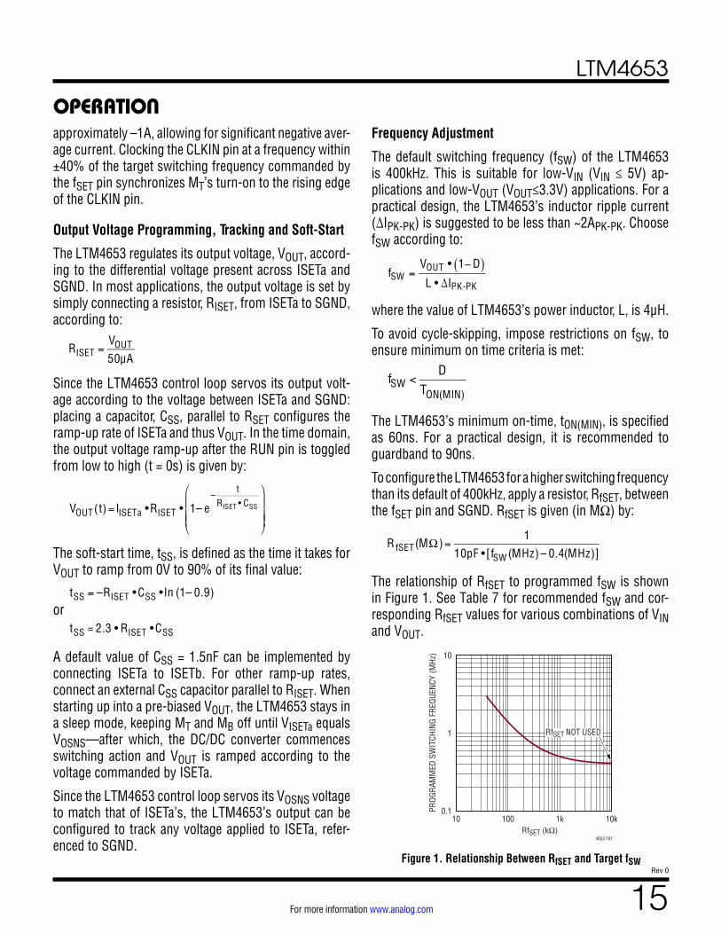
Frequency Adjustment
The default switching frequency (fSW) of the LTM4653 is 400kHz. This is suitable for low-VIN (VIN ≤ 5V) ap-plications and low-VOUT (VOUT≤3.3V) applications. For a practical design, the LTM4653’s inductor ripple current (∆IPK-PK) is suggested to be less than ~2APK-PK. Choose fSW according to:
fSW =
VOUT • 1− D( )L • ∆IPK-PK
where the value of LTM4653’s power inductor, L, is 4μH.
To avoid cycle-skipping, impose restrictions on fSW, to ensure minimum on time criteria is met:
fSW <
DTON(MIN)
The LTM4653’s minimum on-time, tON(MIN), is specified as 60ns. For a practical design, it is recommended to guardband to 90ns.
To configure the LTM4653 for a higher switching frequency than its default of 400kHz, apply a resistor, RfSET, between the fSET pin and SGND. RfSET is given (in MΩ) by:
R fSET(MΩ) =
110pF •[fSW (MHz) – 0.4(MHz)]
The relationship of RfSET to programmed fSW is shown in Figure 1. See Table 7 for recommended fSW and cor-responding RfSET values for various combinations of VIN and VOUT.
RfSET NOT USED
RfSET (kΩ)10 100 1k 10k
0.1
1
10
PROG
RAM
MED
SW
ITCH
ING
FREQ
UENC
Y (M
Hz)
4653 F01
Figure 1. Relationship Between RfSET and Target fSW
LTM4653
16Rev 0
For more information www.analog.com
Power Module Protection
The LTM4653’s current mode control architecture provides fast cycle-by-cycle current limit in an overcurrent condition, as shown in the Typical Performance Characteristics sec-tion. If the output voltage collapses sufficiently due to an overload or short-circuit condition, minimum on-time will be violated and the internal oscillator will then fold-back automatically to one-fifth of the LTM4653’s programmed switching frequency—thereby reducing the output current and affording the load a chance to recover.
The LTM4653 features input overvoltage shutdown protec-tion: when VIN > 68V, switching action ceases (with 4V of hysteresis)—however, be advised that this protection is only active outside the LTM4653’s safe operating area (see Note 1 and Note 4 of the Electrical Characteristics table).
The LTM4653 ceases switching action if internal tempera-tures exceed 165°C. The control IC resumes operation after a 10°C cool-down hysteresis. Note that these typical parameters are based on measurements in a lab oven and are not production tested. This overtemperature protection is intended to protect the device during momentary over-load conditions. The maximum rated junction temperature will be exceeded when this overtemperature protection is active. Continuous operation above the specified absolute maximum operating junction temperature may impair device reliability or permanently damage the device.
The LTM4653 does not feature any specialized output overvoltage protection beyond what is inherent to the control loop’s servo mechanism.
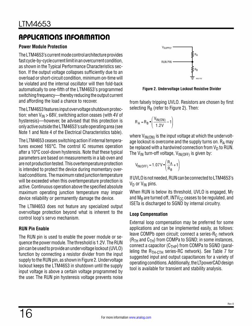
RUN Pin Enable
The RUN pin is used to enable the power module or se-quence the power module. The threshold is 1.2V. The RUN pin can be used to provide an undervoltage lockout (UVLO) function by connecting a resistor divider from the input supply to the RUN pin, as shown in Figure 2. Undervoltage lockout keeps the LTM4653 in shutdown until the supply input voltage is above a certain voltage programmed by the user. The RUN pin hysteresis voltage prevents noise
APPLICATIONS INFORMATION
from falsely tripping UVLO. Resistors are chosen by first selecting RB (refer to Figure 2). Then:
R A = RB •
VIN(ON)
1.2V– 1
⎛
⎝⎜
⎞
⎠⎟
where VIN(ON) is the input voltage at which the undervolt-age lockout is overcome and the supply turns on. RA may be replaced with a hardwired connection from VD to RUN. The VIN turn-off voltage, VIN(OFF) is given by:
VIN(OFF) = 1.07V •
R A
RB+1
⎛
⎝⎜
⎞
⎠⎟
If UVLO is not needed, RUN can be connected to LTM4653’s VD or VIN pins.
When RUN is below its threshold, UVLO is engaged, MT and MB are turned off, INTVCC ceases to be regulated, and ISETa is discharged to SGND by internal circuitry.
Loop Compensation
External loop compensation may be preferred for some applications and can be implemented easily, as follows: leave COMPb open circuit; connect a series-RC network (RTH and CTH) from COMPa to SGND; in some instances, connect a capacitor (CTHP) from COMPa to SGND (paral-leling the RTH-CTH series-RC network). See Table 7 for suggested input and output capacitances for a variety of operating conditions. Additionally, the LTpowerCAD design tool is available for transient and stability analysis.
RUN PIN
RA
RB
VSUPPLY
4653 F02
Figure 2. Undervoltage Lockout Resistive Divider
LTM4653
17Rev 0
For more information www.analog.com
APPLICATIONS INFORMATIONHot-Plugging Safely
The small size, robustness and low impedance of ceramic capacitors make them an attractive option for the input bypass capacitors (CD and CINH) of the LTM4653. However, these capacitors can cause problems if the LTM4653 is plugged into a live supply (see Linear Technology Ap-plication Note 88 for a complete discussion). The low loss ceramic capacitor combined with stray inductance in series with the power source forms an under damped tank circuit, and the voltage at the VIN pin of the LTM4653 can ring to twice the nominal input voltage, possibly ex-ceeding the LTM4653’s rating and damaging the part. If the input supply is poorly controlled or the user will be plugging the LTM4653 into an energized supply, the input network should be designed to prevent this overshoot by introducing a damping element into the path of current flow. This is often done by adding an inexpensive elec-trolytic bulk capacitor (CINL) across the input terminals of the LTM4653. The selection criteria for CINL calls for: an ESR high enough to damp the ringing; a capacitance value several times larger than CINH. CINL does not need to be located physically close to the LTM4653; it should be located close to the application board’s input connec-tor, instead.
INTVCC and EXTVCC Connection
When RUN is logic high, an internal low dropout regula-tor regulates an internal supply, INTVCC, that powers the control circuitry for driving LTM4653’s internal MOSFETs. INTVCC is regulated at 3.3V. In this manner, the LTM4653’s INTVCC is directly powered from SVIN, by default. The gate driver current through the LDO is about 20mA for a typical 1MHz application. The internal LDO power dissipation can be calculated as:
PLDO _ LOSS(INTVCC) = 20mA •(SVIN – 3V)
The LDO draws current off of EXTVCC instead of SVIN when EXTVCC is higher than 3.2V and SVIN is above 5V. For output voltages of 4V and higher, EXTVCC can be con-nected to VOUT through an RC-filter. When the internal LDO derives power from EXTVCC instead of SVIN, the internal LDO power dissipation is:
PLDO _ LOSS(EXTVCC) = 20mA •(VOUT − 3V)
The recommended value of the resistor between VOUT and EXTVCC is roughly VOUT • 4Ω/V. This resistor, REXTVCC, must be rated to continually dissipate (0.02A)² • REXTVCC. The primary purpose of this resistor is to prevent EXTVCC overstress under a fault condition. For example, when an inductive short-circuit is applied to the module’s output, VOUT may be briefly dragged below PGND—forward bias-ing the PGND-to-EXTVCC body diode. This resistor limits the magnitude of current flow in EXTVCC. Bypass EXTVCC with 1μF of X5R (or better) MLCC.
Multiphase Operation
Multiple LTM4653 devices can be paralleled for higher output current applications. For lowest input and output voltage and current ripples, it is advisable to synchronize paralleled LTM4653s to an external clock (within ±40% of the target switching frequency set by fSET—see Test Circuit 1). See Figure 32 for an example of a synchroniz-ing circuit.
LTM4653 modules can be paralleled without synchronizing circuits: just be aware that some beat-frequency ripple will be present in the output voltage and reflected input current by virtue of the fact that such modules are not operating at identical, synchronized switching frequencies.
The LTM4653 device is an inherently current mode con-trolled device, so parallel modules will have good current sharing’s shown in Figure 33. This helps balance the thermals on the design.
To parallel LTM4653s, connect the respective COMPa, ISETa, and VOSNS pins of each LTM4653 together to share the current evenly. In addition, tie the respective RUN pins of paralleled LTM4653 devices together, to ensure proper start-up and shutdown behavior. Figure 32 shows a schematic of LTM4653 devices operating in parallel.
Note that for parallel applications, VOUT can be set by a single, common resistor on the ISETa net:
RISET =
VOUT50µA •N
where N is the number of LTM4653 modules in parallel configuration.
LTM4653
18Rev 0
For more information www.analog.com
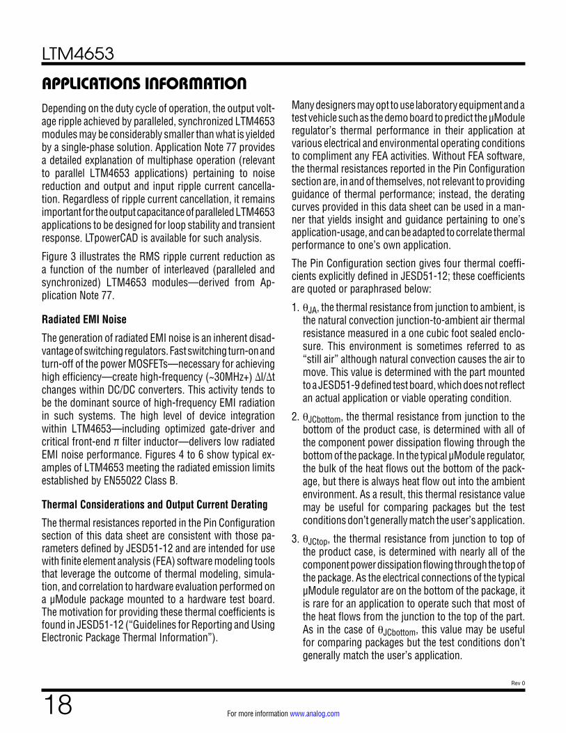
APPLICATIONS INFORMATIONDepending on the duty cycle of operation, the output volt-age ripple achieved by paralleled, synchronized LTM4653 modules may be considerably smaller than what is yielded by a single-phase solution. Application Note 77 provides a detailed explanation of multiphase operation (relevant to parallel LTM4653 applications) pertaining to noise reduction and output and input ripple current cancella-tion. Regardless of ripple current cancellation, it remains important for the output capacitance of paralleled LTM4653 applications to be designed for loop stability and transient response. LTpowerCAD is available for such analysis.
Figure 3 illustrates the RMS ripple current reduction as a function of the number of interleaved (paralleled and synchronized) LTM4653 modules—derived from Ap-plication Note 77.
Radiated EMI Noise
The generation of radiated EMI noise is an inherent disad-vantage of switching regulators. Fast switching turn-on and turn-off of the power MOSFETs—necessary for achieving high efficiency—create high-frequency (~30MHz+) ∆l/∆t changes within DC/DC converters. This activity tends to be the dominant source of high-frequency EMI radiation in such systems. The high level of device integration within LTM4653—including optimized gate-driver and critical front-end filter inductor—delivers low radiated EMI noise performance. Figures 4 to 6 show typical ex-amples of LTM4653 meeting the radiated emission limits established by EN55022 Class B.
Thermal Considerations and Output Current Derating
The thermal resistances reported in the Pin Configuration section of this data sheet are consistent with those pa-rameters defined by JESD51-12 and are intended for use with finite element analysis (FEA) software modeling tools that leverage the outcome of thermal modeling, simula-tion, and correlation to hardware evaluation performed on a µModule package mounted to a hardware test board. The motivation for providing these thermal coefficients is found in JESD51-12 (“Guidelines for Reporting and Using Electronic Package Thermal Information”).
Many designers may opt to use laboratory equipment and a test vehicle such as the demo board to predict the µModule regulator’s thermal performance in their application at various electrical and environmental operating conditions to compliment any FEA activities. Without FEA software, the thermal resistances reported in the Pin Configuration section are, in and of themselves, not relevant to providing guidance of thermal performance; instead, the derating curves provided in this data sheet can be used in a man-ner that yields insight and guidance pertaining to one’s application-usage, and can be adapted to correlate thermal performance to one’s own application.
The Pin Configuration section gives four thermal coeffi-cients explicitly defined in JESD51-12; these coefficients are quoted or paraphrased below:
1. θJA, the thermal resistance from junction to ambient, is the natural convection junction-to-ambient air thermal resistance measured in a one cubic foot sealed enclo-sure. This environment is sometimes referred to as “still air” although natural convection causes the air to move. This value is determined with the part mounted to a JESD51-9 defined test board, which does not reflect an actual application or viable operating condition.
2. θJCbottom, the thermal resistance from junction to the bottom of the product case, is determined with all of the component power dissipation flowing through the bottom of the package. In the typical µModule regulator, the bulk of the heat flows out the bottom of the pack-age, but there is always heat flow out into the ambient environment. As a result, this thermal resistance value may be useful for comparing packages but the test conditions don’t generally match the user’s application.
3. θJCtop, the thermal resistance from junction to top of the product case, is determined with nearly all of the component power dissipation flowing through the top of the package. As the electrical connections of the typical µModule regulator are on the bottom of the package, it is rare for an application to operate such that most of the heat flows from the junction to the top of the part. As in the case of θJCbottom, this value may be useful for comparing packages but the test conditions don’t generally match the user’s application.
LTM4653
19Rev 0
For more information www.analog.com
APPLICATIONS INFORMATION
Figure 3. Normalized Input RMS Ripple Current vs Duty Cycle for One to Six LTM4653s (Phases)
Figure 4. Radiated Emissions Scan of the LTM4653. Producing 24VOUT at 4A, from 29.5VIN. DC2327A Hardware. fSW = 1.2MHz. Measured in a 10m Chamber. Peak Detect Method
0.75 0.8
4653 F03
0.70.650.60.550.50.450.40.350.30.250.20.150.1 0.85 0.9DUTY CYCLE
0
DC L
OAD
CURR
ENT
RMS
INPU
T RI
PPLE
CUR
RENT
0.05
0.10
0.15
0.20
0.25
0.30
0.35
0.40
0.45
0.50
0.55
0.601-PHASE2-PHASE3-PHASE4-PHASE6-PHASE
AMPL
ITUD
E (d
BµV/
m)
50
60
70
40
30
20
10
–10
0
FREQUENCY (MHz)30 830130 230 330 430 530 630 730 930 1000
4653 F04
[1] HORIZONTAL[2] VERTICALQPK LIMITFORMAL
MEAS DIST 10mSPEC DIST 10m
+
AMPL
ITUD
E (d
BµV/
m)
50
60
70
40
30
20
10
–10
0
FREQUENCY (MHz)30 830130 230 330 430 530 630 730 930 1000
4653 F05
[1] HORIZONTAL[2] VERTICALQPK LIMITFORMAL
MEAS DIST 10mSPEC DIST 10m
+
AMPL
ITUD
E (d
BµV/
m)
50
60
70
40
30
20
10
–10
0
FREQUENCY (MHz)30 830130 230 330 430 530 630 730 930 1000
4653 F06
[1] HORIZONTAL[2] VERTICALQPK LIMITFORMAL
MEAS DIST 10mSPEC DIST 10m
+
Figure 5. Radiated Emissions Scan of the LTM4653 Producing 24VOUT at 3.5A, from 48VIN. DC2327A Hardware. fSW = 1.2MHz. Measured in a 10m Chamber. Peak Detect Method
Figure 6. Radiated Emissions Scan of the LTM4653. Producing 12VOUT at 3A, from 58VIN. DC2327A Hardware. fSW = 1.2MHz. Measured in a 10m Chamber. Peak Detect Method

LTM4653
20Rev 0
For more information www.analog.com
4. θJB, the thermal resistance from junction to the printed circuit board, is the junction-to-board thermal resis-tance where almost all of the heat flows through the bottom of the µModule regulator and into the board, and is really the sum of the θJCbottom and the thermal resistance of the bottom of the part through the solder joints and through a portion of the board. The board temperature is measured a specified distance from the package, using a two sided, two layer board. This board is described in JESD51-9.
A graphical representation of the aforementioned ther-mal resistances is given in Figure 7; blue resistances are contained within the µModule regulator, whereas green resistances are external to the µModule package.
As a practical matter, it should be clear to the reader that no individual or sub-group of the four thermal resistance parameters defined by JESD51-12 or provided in the Pin Configuration section replicates or conveys normal operating conditions of a µModule regulator. For example, in normal board-mounted applications, never does 100% of the device’s total power loss (heat) thermally conduct exclusively through the top or exclusively through bot-tom of the µModule package—as the standard defines for θJCtop and θJCbottom, respectively. In practice, power loss is thermally dissipated in both directions away from the package—granted, in the absence of a heat sink and airflow, a majority of the heat flow is into the board.
Within the LTM4653, be aware there are multiple power devices and components dissipating power, with a con-sequence that the thermal resistances relative to different junctions of components or die are not exactly linear with respect to total package power loss. To reconcile this complication without sacrificing modeling simplicity—but also not ignoring practical realities—an approach has been taken using FEA software modeling along with laboratory testing in a controlled-environment chamber to reason-ably define and correlate the thermal resistance values supplied in this data sheet: (1) Initially, FEA software is used to accurately build the mechanical geometry of the LTM4653 and the specified PCB with all of the correct material coefficients along with accurate power loss source definitions; (2) this model simulates a software-defined JEDEC environment consistent with JESD51-9 and JESD51-12 to predict power loss heat flow and temperature readings at different interfaces that enable the calculation of the JEDEC-defined thermal resistance values; (3) the model and FEA software is used to evaluate the LTM4653 with heat sink and airflow; (4) having solved for and analyzed these thermal resistance values and simulated various operating conditions in the software model, a thorough laboratory evaluation replicates the simulated conditions with thermocouples within a controlled envi-ronment chamber while operating the device at the same power loss as that which was simulated. The outcome of this process and due diligence yields the set of derating
APPLICATIONS INFORMATION
4653 F07
µModule DEVICE
JUNCTION-TO-CASE (TOP)RESISTANCE
JUNCTION-TO-BOARD RESISTANCE
JUNCTION-TO-AMBIENT THERMAL RESISTANCE COMPONENTS
CASE (TOP)-TO-AMBIENTRESISTANCE
BOARD-TO-AMBIENTRESISTANCE
JUNCTION-TO-CASE(BOTTOM) RESISTANCE
JUNCTION AMBIENT
CASE (BOTTOM)-TO-BOARDRESISTANCE
Figure 7. Graphical Representaion of JESD51-12 Thermal Coefficients
LTM4653
21Rev 0
For more information www.analog.com
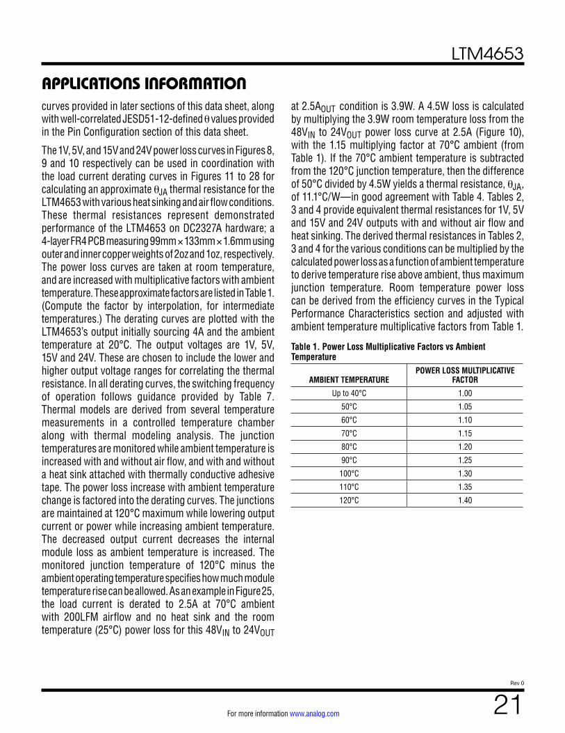
curves provided in later sections of this data sheet, along with well-correlated JESD51-12-defined θ values provided in the Pin Configuration section of this data sheet.
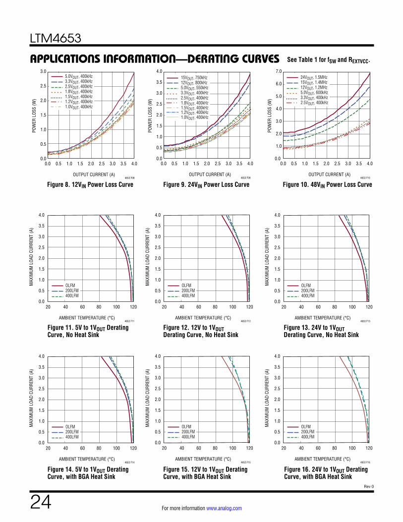
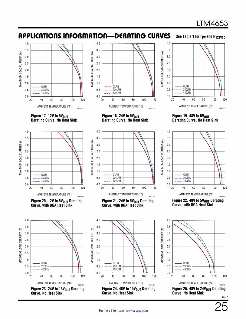
The 1V, 5V, and 15V and 24V power loss curves in Figures 8, 9 and 10 respectively can be used in coordination with the load current derating curves in Figures 11 to 28 for calculating an approximate θJA thermal resistance for the LTM4653 with various heat sinking and air flow conditions. These thermal resistances represent demonstrated performance of the LTM4653 on DC2327A hardware; a 4-layer FR4 PCB measuring 99mm × 133mm × 1.6mm using outer and inner copper weights of 2oz and 1oz, respectively. The power loss curves are taken at room temperature, and are increased with multiplicative factors with ambient temperature. These approximate factors are listed in Table 1. (Compute the factor by interpolation, for intermediate temperatures.) The derating curves are plotted with the LTM4653’s output initially sourcing 4A and the ambient temperature at 20°C. The output voltages are 1V, 5V, 15V and 24V. These are chosen to include the lower and higher output voltage ranges for correlating the thermal resistance. In all derating curves, the switching frequency of operation follows guidance provided by Table 7. Thermal models are derived from several temperature measurements in a controlled temperature chamber along with thermal modeling analysis. The junction temperatures are monitored while ambient temperature is increased with and without air flow, and with and without a heat sink attached with thermally conductive adhesive tape. The power loss increase with ambient temperature change is factored into the derating curves. The junctions are maintained at 120°C maximum while lowering output current or power while increasing ambient temperature. The decreased output current decreases the internal module loss as ambient temperature is increased. The monitored junction temperature of 120°C minus the ambient operating temperature specifies how much module temperature rise can be allowed. As an example in Figure 25, the load current is derated to 2.5A at 70°C ambient with 200LFM airflow and no heat sink and the room temperature (25°C) power loss for this 48VIN to 24VOUT
at 2.5AOUT condition is 3.9W. A 4.5W loss is calculated by multiplying the 3.9W room temperature loss from the 48VIN to 24VOUT power loss curve at 2.5A (Figure 10), with the 1.15 multiplying factor at 70°C ambient (from Table 1). If the 70°C ambient temperature is subtracted from the 120°C junction temperature, then the difference of 50°C divided by 4.5W yields a thermal resistance, θJA, of 11.1°C/W—in good agreement with Table 4. Tables 2, 3 and 4 provide equivalent thermal resistances for 1V, 5V and 15V and 24V outputs with and without air flow and heat sinking. The derived thermal resistances in Tables 2, 3 and 4 for the various conditions can be multiplied by the calculated power loss as a function of ambient temperature to derive temperature rise above ambient, thus maximum junction temperature. Room temperature power loss can be derived from the efficiency curves in the Typical Performance Characteristics section and adjusted with ambient temperature multiplicative factors from Table 1.
Table 1. Power Loss Multiplicative Factors vs Ambient Temperature
AMBIENT TEMPERATUREPOWER LOSS MULTIPLICATIVE
FACTOR
Up to 40°C 1.00
50°C 1.05
60°C 1.10
70°C 1.15
80°C 1.20
90°C 1.25
100°C 1.30
110°C 1.35
120°C 1.40
APPLICATIONS INFORMATION
LTM4653
22Rev 0
For more information www.analog.com
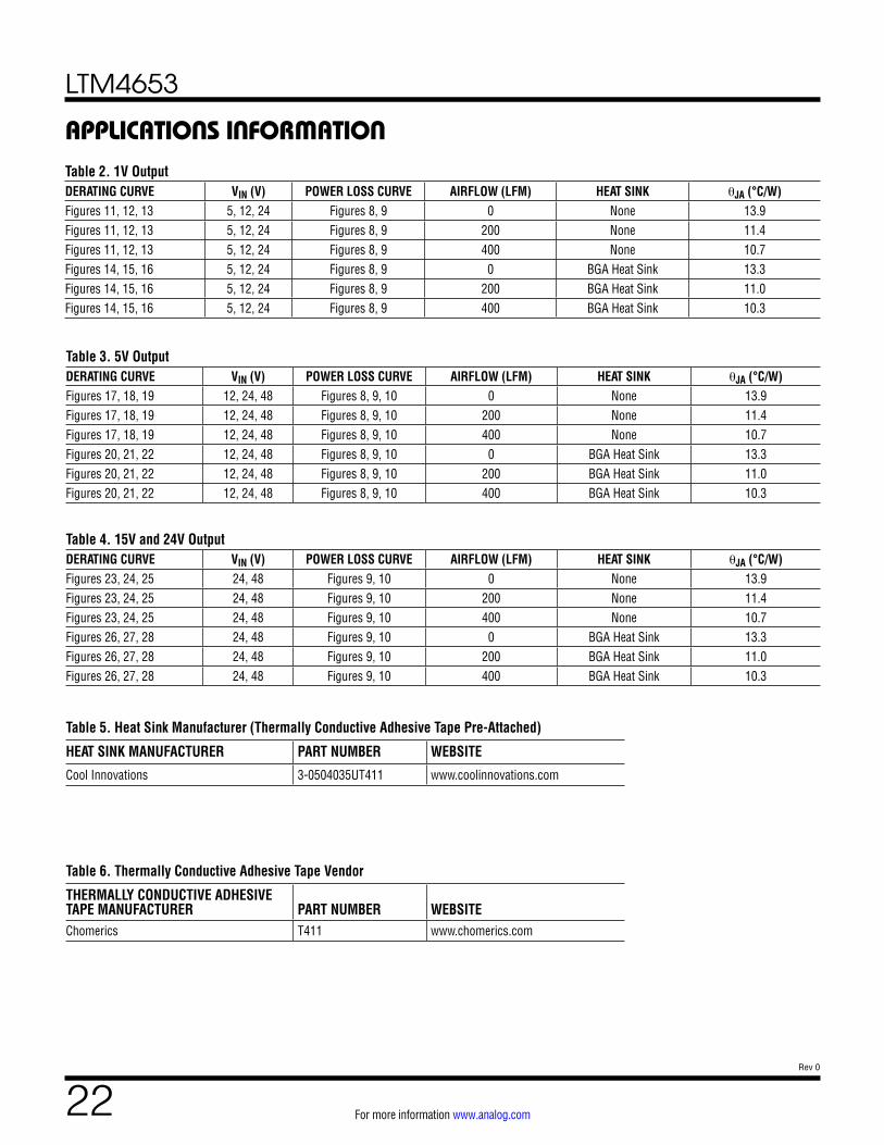
Table 2. 1V OutputDERATING CURVE VIN (V) POWER LOSS CURVE AIRFLOW (LFM) HEAT SINK θJA (°C/W)Figures 11, 12, 13 5, 12, 24 Figures 8, 9 0 None 13.9Figures 11, 12, 13 5, 12, 24 Figures 8, 9 200 None 11.4Figures 11, 12, 13 5, 12, 24 Figures 8, 9 400 None 10.7Figures 14, 15, 16 5, 12, 24 Figures 8, 9 0 BGA Heat Sink 13.3Figures 14, 15, 16 5, 12, 24 Figures 8, 9 200 BGA Heat Sink 11.0Figures 14, 15, 16 5, 12, 24 Figures 8, 9 400 BGA Heat Sink 10.3
Table 3. 5V OutputDERATING CURVE VIN (V) POWER LOSS CURVE AIRFLOW (LFM) HEAT SINK θJA (°C/W)Figures 17, 18, 19 12, 24, 48 Figures 8, 9, 10 0 None 13.9Figures 17, 18, 19 12, 24, 48 Figures 8, 9, 10 200 None 11.4Figures 17, 18, 19 12, 24, 48 Figures 8, 9, 10 400 None 10.7Figures 20, 21, 22 12, 24, 48 Figures 8, 9, 10 0 BGA Heat Sink 13.3Figures 20, 21, 22 12, 24, 48 Figures 8, 9, 10 200 BGA Heat Sink 11.0Figures 20, 21, 22 12, 24, 48 Figures 8, 9, 10 400 BGA Heat Sink 10.3
Table 4. 15V and 24V OutputDERATING CURVE VIN (V) POWER LOSS CURVE AIRFLOW (LFM) HEAT SINK θJA (°C/W)Figures 23, 24, 25 24, 48 Figures 9, 10 0 None 13.9Figures 23, 24, 25 24, 48 Figures 9, 10 200 None 11.4Figures 23, 24, 25 24, 48 Figures 9, 10 400 None 10.7Figures 26, 27, 28 24, 48 Figures 9, 10 0 BGA Heat Sink 13.3Figures 26, 27, 28 24, 48 Figures 9, 10 200 BGA Heat Sink 11.0Figures 26, 27, 28 24, 48 Figures 9, 10 400 BGA Heat Sink 10.3
Table 5. Heat Sink Manufacturer (Thermally Conductive Adhesive Tape Pre-Attached)
HEAT SINK MANUFACTURER PART NUMBER WEBSITE
Cool Innovations 3-0504035UT411 www.coolinnovations.com
Table 6. Thermally Conductive Adhesive Tape Vendor
THERMALLY CONDUCTIVE ADHESIVE TAPE MANUFACTURER PART NUMBER WEBSITEChomerics T411 www.chomerics.com
APPLICATIONS INFORMATION
LTM4653
23Rev 0
For more information www.analog.com
APPLICATIONS INFORMATIONTable 7. LTM4653 Output Voltage Response vs Component Matrix. Performance of Figure 30 Circuit with Values Here Indicated. Load-Stepping from 2A to 4A Load Current, at 2A/μs. Typical Measured ValuesCOUTH VENDORS PART NUMBER COUTH VENDORS PART NUMBER
AVX 12066D107MAT2A (100μF, 6.3V, 1206 Case Size) AVX 12105D106MAT2A (10μF, 50V, 1210 Case Size)
Murata GRM31CR60J107M (100μF, 6.3V, 1206 Case Size) Murata GRM32ER61H106M (10μF, 50V, 1210 Case Size)
Taiyo Yuden JMK316BBJ107MLHT (100μF, 6.3V, 1206 Case Size) Taiyo Yuden UMK325BJ106M (10μF, 50V, 1210 Case Size)
TDK C3216X5R0J107M (100μF, 6.3V, 1206 Case Size) TDK C3225X5R1H106M (10μF, 50V, 1210 Case Size)
AVX 1210YD476MAT2A (47μF, 16V, 1210 Case Size) CINH/CD VENDORS PART NUMBER
Murata GRM32ER61C476M (47μF, 16V, 1210 Case Size) Murata GRM32ER71K475M (4.7μF, 80V, 1210 Case Size)
Taiyo Yuden EMK325BJ476MM (47μF, 16V, 1210 Case Size) AVX 12065C475MAT2A (4.7μF, 50V, 1206 Case Size)
AVX 12103D226MAT2A (22μF, 25V, 1210 Case Size) Murata GRM31CR71H475M (4.7μF, 50V, 1206 Case Size)
Taiyo Yuden TMK325BJ226MM (22μF, 25V, 1210 Case Size) Taiyo Yuden UMK316AB7475ML (4.7μF, 50V, 1206 Case Size)
TDK C3225X5R1E226M (22μF, 25V, 1210 Case Size) TDK C3216X5R1H475M (4.7μF, 50V, 1206 Case Size)
VOUT
(V)VIN (V) CINH CD COUTH
RTH (Ω)
CTH (nF)
RISET (kΩ)
RPGDFB (kΩ)
fSW (kHz)
RfSET (kΩ)
REXTVCC (Ω)
LOAD STEP TRANSIENT
DROOP (mV)
LOAD STEP PK-PK
DEVIATION (mV)
RECOVERY TIME (μs)
1 5 4.7μF 4.7μF 100μF x 3 681 6.8 20 3.32 400 N/A N/A 70 145 551 12 4.7μF 4.7μF 100μF x 3 681 6.8 20 3.32 400 N/A N/A 70 145 501 24 4.7μF 4.7μF 100μF x 3 681 6.8 20 3.32 400 N/A N/A 70 145 50
1.2 5 4.7μF 4.7μF 100μF x 3 665 6.8 24 4.99 400 N/A N/A 70 145 501.2 12 4.7μF 4.7μF 100μF x 3 665 6.8 24 4.99 400 N/A N/A 70 145 501.2 24 4.7μF 4.7μF 100μF x 3 665 6.8 24 4.99 400 N/A N/A 70 145 501.5 5 4.7μF 4.7μF 100μF x 3 665 6.8 30.1 7.5 400 N/A N/A 70 145 501.5 12 4.7μF 4.7μF 100μF x 3 665 6.8 30.1 7.5 400 N/A N/A 70 145 501.5 24 4.7μF 4.7μF 100μF x 3 665 6.8 30.1 7.5 400 N/A N/A 70 145 501.5 36 4.7μF 4.7μF 100μF x 3 665 6.8 30.1 7.5 400 N/A N/A 70 145 501.8 5 4.7μF 4.7μF 100μF x 3 665 8.2 36 10 400 N/A N/A 70 145 501.8 12 4.7μF 4.7μF 100μF x 3 665 8.2 36 10 400 N/A N/A 70 145 501.8 24 4.7μF 4.7μF 100μF x 3 665 8.2 36 10 400 N/A N/A 70 145 501.8 36 4.7μF 4.7μF 100μF x 3 665 8.2 36 10 400 N/A N/A 70 145 502.5 5 4.7μF 4.7μF 100μF x 3 649 8.2 50 15.8 400 N/A N/A 70 145 502.5 12 4.7μF 4.7μF 100μF x 3 649 8.2 50 15.8 400 N/A N/A 70 145 502.5 24 4.7μF 4.7μF 100μF x 3 649 8.2 50 15.8 400 N/A N/A 70 145 502.5 36 4.7μF 4.7μF 100μF x 3 649 8.2 50 15.8 400 N/A N/A 70 145 502.5 48 4.7μF 4.7μF 100μF x 3 649 8.2 50 15.8 400 N/A N/A 70 145 503.3 5 4.7μF 4.7μF 100μF x 2 604 10 66.5 22.6 400 N/A N/A 90 190 503.3 12 4.7μF 4.7μF 100μF x 2 604 10 66.5 22.6 400 N/A N/A 90 190 503.3 24 4.7μF 4.7μF 100μF x 2 604 10 66.5 22.6 400 N/A N/A 90 185 503.3 36 4.7μF 4.7μF 100μF x 2 604 10 66.5 22.6 400 N/A N/A 90 180 503.3 48 4.7μF 4.7μF 100μF x 2 604 10 66.5 22.6 400 N/A N/A 90 180 505 12 4.7μF 4.7μF 47μF x 2 499 10 100 36.5 400 N/A 20 130 260 455 24 4.7μF 4.7μF 47μF x 2 499 10 100 36.5 550 665 20 130 260 455 36 4.7μF 4.7μF 47μF x 2 499 10 100 36.5 575 576 20 130 260 455 48 4.7μF 4.7μF 47μF x 2 499 10 100 36.5 600 499 20 130 260 45
12 15 4.7μF 4.7μF 22μF x 2 499 10 240 95.3 500 1000 49.9 170 350 4012 24 4.7μF 4.7μF 22μF x 2 499 10 240 95.3 800 249 49.9 170 350 4012 36 4.7μF 4.7μF 22μF x 2 499 10 240 95.3 1100 143 49.9 170 350 4012 48 4.7μF 4.7μF 22μF x 2 499 10 240 95.3 1200 124 49.9 170 350 4015 24 4.7μF 4.7μF 22μF x 2 499 10 301 121 750 287 60.4 170 350 4015 36 4.7μF 4.7μF 22μF x 2 499 10 301 121 1200 124 60.4 170 350 4015 48 4.7μF 4.7μF 22μF x 2 499 10 301 121 1400 100 60.4 170 350 4024 36 4.7μF 4.7μF 10μF x 2 499 10 481 196 1200 124 100 220 430 3524 48 4.7μF 4.7μF 10μF x 2 499 10 481 196 1500 90.9 100 220 440 35
LTM4653
24Rev 0
For more information www.analog.com
APPLICATIONS INFORMATION—DERATING CURVES
Figure 8. 12VIN Power Loss Curve Figure 9. 24VIN Power Loss Curve Figure 10. 48VIN Power Loss Curve
See Table 1 for fSW and REXTVCC.
0.0
0.5
1.0
1.5
2.0
2.5
3.0
0.0 0.5 1.0 1.5 2.0 2.5 3.0 3.5 4.0
POW
ER L
OSS
(W)
OUTPUT CURRENT (A) 4653 F08
1.5VOUT, 400kHz1.8VOUT, 400kHz2.5VOUT, 400kHz3.3VOUT, 400kHz5.0VOUT, 400kHz
1.2VOUT, 400kHz1.0VOUT, 400kHz
0.0
0.5
1.5
1.0
2.0
3.5
3.0
2.5
4.0
0.0 0.5 1.0 1.5 2.0 2.5 3.0 3.5 4.0
POW
ER L
OSS
(W)
OUTPUT CURRENT (A) 4653 F09
2.5VOUT, 400kHz3.3VOUT, 400kHz5.0VOUT, 550kHz12VOUT, 800kHz15VOUT, 750kHz
1.8VOUT, 400kHz1.5VOUT, 400kHz1.2VOUT, 400kHz1.0VOUT, 400kHz
0.0
1.0
2.0
5.0
4.0
3.0
6.0
7.0
0.0 0.5 1.0 1.5 2.0 2.5 3.0 3.5 4.0
POW
ER L
OSS
(W)
OUTPUT CURRENT (A) 4653 F10
3.3VOUT, 400kHz5.0VOUT, 600kHz12VOUT, 1.2MHz15VOUT, 1.4MHz24VOUT, 1.5MHz
2.5VOUT, 400kHz
20 40 60 80 100 120
AMBIENT TEMPERATURE (°C) 4653 F12
0.0
0.5
1.0
1.5
2.0
2.5
3.0
3.5
4.0
MAX
IMUM
LOA
D CU
RREN
T (A
)
400LFM200LFMOLFM
20 40 60 80 100 120
AMBIENT TEMPERATURE (°C) 4653 F13
0.0
0.5
1.0
1.5
2.0
2.5
3.0
3.5
4.0
MAX
IMUM
LOA
D CU
RREN
T (A
)
400LFM200LFMOLFM
20 40 60 80 100 120
AMBIENT TEMPERATURE (°C) 4653 F14
0.0
0.5
1.0
1.5
2.0
2.5
3.0
3.5
4.0
MAX
IMUM
LOA
D CU
RREN
T (A
)
400LFM200LFMOLFM
20 40 60 80 100 120
AMBIENT TEMPERATURE (°C) 4653 F15
0.0
0.5
1.0
1.5
2.0
2.5
3.0
3.5
4.0
MAX
IMUM
LOA
D CU
RREN
T (A
)
400LFM200LFMOLFM
20 40 60 80 100 120
AMBIENT TEMPERATURE (°C) 4653 F16
0.0
0.5
1.0
1.5
2.0
2.5
3.0
3.5
4.0
MAX
IMUM
LOA
D CU
RREN
T (A
)
400LFM200LFMOLFM
20 40 60 80 100 120
AMBIENT TEMPERATURE (°C) 4653 F11
0.0
0.5
1.0
1.5
2.0
2.5
3.0
3.5
4.0
MAX
IMUM
LOA
D CU
RREN
T (A
)
400LFM200LFMOLFM
Figure 11. 5V to 1VOUT Derating Curve, No Heat Sink
Figure 12. 12V to 1VOUT Derating Curve, No Heat Sink
Figure 13. 24V to 1VOUT Derating Curve, No Heat Sink
Figure 14. 5V to 1VOUT Derating Curve, with BGA Heat Sink
Figure 15. 12V to 1VOUT Derating Curve, with BGA Heat Sink
Figure 16. 24V to 1VOUT Derating Curve, with BGA Heat Sink
LTM4653
25Rev 0
For more information www.analog.com
Figure 17. 12V to 5VOUT Derating Curve, No Heat Sink
APPLICATIONS INFORMATION—DERATING CURVES See Table 1 for fSW and REXTVCC.
20 40 60 80 100 120
AMBIENT TEMPERATURE (°C) 4653 F17
0.0
0.5
1.0
1.5
2.0
2.5
3.0
3.5
4.0
MAX
IMUM
LOA
D CU
RREN
T (A
)
400LFM200LFMOLFM
20 40 60 80 100 120
AMBIENT TEMPERATURE (°C) 4653 F18
0.0
0.5
1.0
1.5
2.0
2.5
3.0
3.5
4.0
MAX
IMUM
LOA
D CU
RREN
T (A
) 400LFM200LFMOLFM
20 40 60 80 100 120
AMBIENT TEMPERATURE (°C) 4653 F19
0.0
0.5
1.0
1.5
2.0
2.5
3.0
3.5
4.0
MAX
IMUM
LOA
D CU
RREN
T (A
)
400LFM200LFMOLFM
20 40 60 80 100 120
AMBIENT TEMPERATURE (°C) 4653 F20
0.0
0.5
1.0
1.5
2.0
2.5
3.0
3.5
4.0
MAX
IMUM
LOA
D CU
RREN
T (A
)
400LFM200LFMOLFM
20 40 60 80 100 120
AMBIENT TEMPERATURE (°C) 4653 F21
0.0
0.5
1.0
1.5
2.0
2.5
3.0
3.5
4.0
MAX
IMUM
LOA
D CU
RREN
T (A
)
400LFM200LFMOLFM
20 40 60 80 100 120
AMBIENT TEMPERATURE (°C) 4653 F22
0.0
0.5
1.0
1.5
2.0
2.5
3.0
3.5
4.0
MAX
IMUM
LOA
D CU
RREN
T (A
)
400LFM200LFMOLFM
20 40 60 80 100 120
AMBIENT TEMPERATURE (°C) 4653 F23
0.0
0.5
1.0
1.5
2.0
2.5
3.0
3.5
4.0
MAX
IMUM
LOA
D CU
RREN
T (A
)
400LFM200LFMOLFM
20 40 60 80 100 120
AMBIENT TEMPERATURE (°C) 4653 F24
0.0
0.5
1.0
1.5
2.0
2.5
3.0
3.5
4.0
MAX
IMUM
LOA
D CU
RREN
T (A
)
400LFM200LFMOLFM
20 40 60 80 100 120
AMBIENT TEMPERATURE (°C) 4653 F25
0.0
0.5
1.0
1.5
2.0
2.5
3.0
3.5
4.0
MAX
IMUM
LOA
D CU
RREN
T (A
)
400LFM200LFMOLFM
Figure 18. 24V to 5VOUT Derating Curve, No Heat Sink
Figure 19. 48V to 5VOUT Derating Curve, No Heat Sink
Figure 20. 12V to 5VOUT Derating Curve, with BGA Heat Sink
Figure 21. 24V to 5VOUT Derating Curve, with BGA Heat Sink
Figure 22. 48V to 5VOUT Derating Curve, with BGA Heat Sink
Figure 23. 24V to 15VOUT Derating Curve, No Heat Sink
Figure 24. 48V to 15VOUT Derating Curve, No Heat Sink
Figure 25. 48V to 24VOUT Derating Curve, No Heat Sink

LTM4653
26Rev 0
For more information www.analog.com
Figure 26. 24V to 15VOUT Derating Curve, with BGA Heat Sink
Figure 27. 48V to 15VOUT Derating Curve, with BGA Heat Sink
Figure 28. 48V to 24VOUT Derating Curve, with BGA Heat Sink
APPLICATIONS INFORMATION—DERATING CURVES
APPLICATIONS INFORMATIONSafety Considerations
The LTM4653 does not provide galvanic isolation from VIN to VOUT. There is no internal fuse. If required, a slow blow fuse with a rating twice the maximum input current needs to be provided to protect the unit from catastrophic failure.
The fuse or circuit breaker, if used, should be selected to limit the current to the regulator in case of a MT MOSFET fault. If MT fails, the system’s input supply will source very large currents to VOUT through MT. This can cause excessive heat and board damage depending on how much power the input voltage can deliver to this system. A fuse or circuit breaker can be used as a secondary fault protector in this situation. The LTM4653 does feature overcurrent and overtemperature protection.
Layout Checklist/Example
The high integration of LTM4653 makes the PCB board layout straightforward. However, to optimize its electrical and thermal performance, some layout considerations are still necessary.
• Use large PCB copper areas for high current paths, including VIN, PGND and VOUT. Doing so helps to minimize the PCB conduction loss and thermal stress.
• Place high frequency ceramic input and output ca-pacitors next to the VIN, VD, PGND and VOUT pins to minimize high frequency noise.
• Place a dedicated power ground layer underneath the LTM4653.
• To minimize the via conduction loss and reduce module thermal stress, use multiple vias for interconnection between top layer and other power layers.
• Do not put vias directly on pads, unless they are capped or plated over.
• Use a separate SGND copper plane for components connected to signal pins. Connect SGND to PGND directly under the module.
• For parallel module applications, connect the VOUT, VOSNS, RUN, ISETa, COMPa and PGOOD pins together as shown in Figure 32.
• Bring out test points on the signal pins for monitoring.
Figure 29 gives a good example of the recommended LTM4653 layout.
20 40 60 80 100 120
AMBIENT TEMPERATURE (°C) 4653 F26
0.0
0.5
1.0
1.5
2.0
2.5
3.0
3.5
4.0
MAX
IMUM
LOA
D CU
RREN
T (A
)
400LFM200LFMOLFM
20 40 60 80 100 120
AMBIENT TEMPERATURE (°C) 4653 F27
0.0
0.5
1.0
1.5
2.0
2.5
3.0
3.5
4.0
MAX
IMUM
LOA
D CU
RREN
T (A
) 400LFM200LFMOLFM
20 40 60 80 100 120
AMBIENT TEMPERATURE (°C) 4653 F28
0.0
0.5
1.0
1.5
2.0
2.5
3.0
3.5
4.0
MAX
IMUM
LOA
D CU
RREN
T (A
)
400LFM200LFMOLFM
See Table 1 for fSW and REXTVCC.
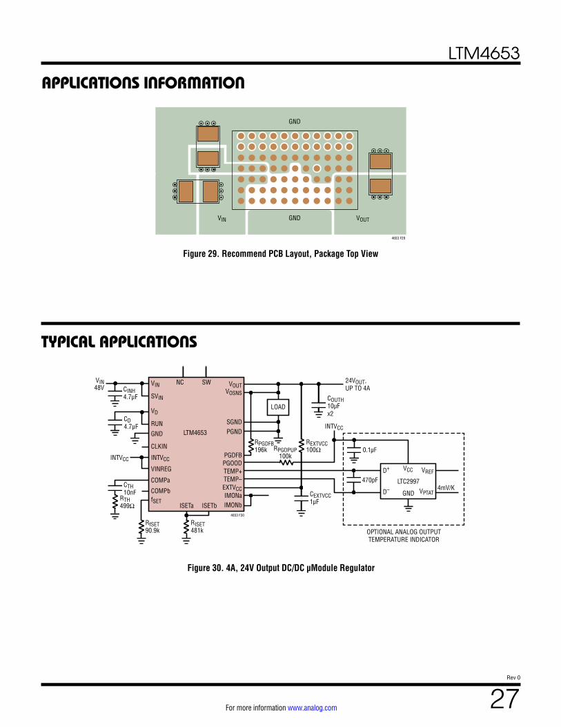
LTM4653
27Rev 0
For more information www.analog.com
APPLICATIONS INFORMATION
Figure 29. Recommend PCB Layout, Package Top View
TYPICAL APPLICATIONS
Figure 30. 4A, 24V Output DC/DC μModule Regulator
GND
VIN VOUTGND
4653 F29
VIN
SVIN
VD
RUN
GND
VOUTVOSNS
PGND
PGOOD
IMONaIMONbISETbISETa
TEMP+TEMP–EXTVCC
PGDFB
24VOUT,UP TO 4A
COUTH10µFx2
SGND
RPGDFB196k RPGDPUP
100k
REXTVCC100Ω
CEXTVCC1µF
0.1µF
470pF
RISET481k
RfSET90.9k
CD4.7μF
CINH4.7μF
INTVCCINTVCC
INTVCC
CTH10nF
VINREG
CLKIN
4653 F30
NC SW
LTM4653
OPTIONAL ANALOG OUTPUTTEMPERATURE INDICATOR
COMPa
COMPbfSET
VIN48V
LOAD
D+
D–
VCC VREF
VPTATGND
LTC29974mV/K
RTH499Ω
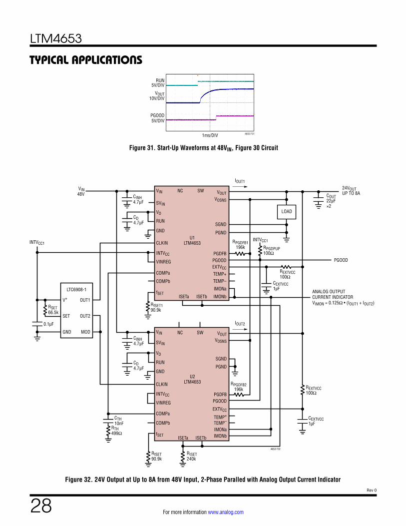
LTM4653
28Rev 0
For more information www.analog.com
Figure 31. Start-Up Waveforms at 48VIN, Figure 30 Circuit
1ms/DIV
VOUT10V/DIV
PGOOD5V/DIV
RUN5V/DIV
4653 F31
Figure 32. 24V Output at Up to 8A from 48V Input, 2-Phase Paralled with Analog Output Current Indicator
TYPICAL APPLICATIONS
ISETa ISETb
U2LTM4653
RfSET90.9k
RISET240k
CTH10nF
RTH499Ω fSET
4653 F32
ISETa ISETb
U1LTM4653
24VOUT UP TO 8A
LOAD
RfSET190.9k
CD4.7μF
CINH4.7μF
fSET
CINH4.7μF
CD4.7μF
RPGDFB1196k
REXTVCC100Ω
RPGDPUP100Ω
CEXTVCC1µF
COUT22µF×2
OUT1
OUT2
MOD
VIN48V
V+
SET
GND
LTC6908-1
RSET66.5k
INTVCC1
0.1µF
REXTVCC100Ω
CEXTVCC1µF
RPGDFB2196k
VOUT
IOUT1
VOSNS
EXTVCC
SGND
PGND
PGDFBPGOOD PGOOD
ANALOG OUTPUTCURRENT INDICATORVIMON = 0.125Ω • (IOUT1 + IOUT2)
IMONa
IMONb
TEMP+TEMP–
COMPa
COMPb
VINREG
INTVCC
CLKIN
GND
RUN
NC SW
VD
SVIN
VIN
VOUTVOSNS
PGND
PGDFB
IMONaIMONb
PGOOD
SGND
EXTVCC
TEMP+
TEMP–
COMPa
COMPb
VINREG
INTVCC
CLKIN
GND
RUN
NC SW
VD
SVIN
VIN
INTVCC1
IOUT2

LTM4653
29Rev 0
For more information www.analog.com
Figure 33. Current Sharing Performance of LTM4653s in Figure 32 Circuit
Figure 34. Concurrent ±12V Supply, Output Voltage Start-Up Waveforms, Figure 35 Circuit
TYPICAL APPLICATIONS
0 1 2 3 4 5 6 7 8
TOTAL OUTPUT CURRENT (A) 4653 F33
–1
0
1
2
3
4
5
MOD
ULE
OUTP
UT C
URRE
NT (A
)
U2U1
2ms/DIV
VOUT5V/DIV
VOUT–
5V/DIV
PGOOD5V/DIV
RUN5V/DIV
4653 F34
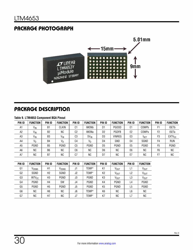
LTM4653
30Rev 0
For more information www.analog.com
PACKAGE DESCRIPTIONTable 9. LTM4653 Component BGA Pinout
PIN ID FUNCTION PIN ID FUNCTION PIN ID FUNCTION PIN ID FUNCTION PIN ID FUNCTION PIN ID FUNCTION
A1 VIN B1 CLKIN C1 IMONb D1 PGOOD E1 COMPb F1 ISETb
A2 VIN B2 NC C2 IMONa D2 PGDFB E2 COMPa F2 ISETa
A3 VIN B3 VIN C3 SVIN D3 VINREG E3 fSET F3 EXTVCC
A4 VD B4 VD C4 VD D4 GND E4 SGND F4 RUN
A5 PGND B5 PGND C5 PGND D5 PGND E5 PGND F5 PGND
A6 NC B6 NC C6 NC D6 NC E6 NC F6 NC
A7 NC B7 NC C7 NC D7 NC E7 NC F7 NC
PIN ID FUNCTION PIN ID FUNCTION PIN ID FUNCTION PIN ID FUNCTION PIN ID FUNCTION
G1 VOSNS H1 VOSNS J1 TEMP+ K1 VOUT L1 VOUT
G2 SGND H2 SGND J2 TEMP– K2 VOUT L2 VOUT
G3 INTVCC H3 PGND J3 PGND K3 VOUT L3 VOUT
G4 PGND H4 SW J4 PGND K4 PGND L4 PGND
G5 PGND H5 PGND J5 PGND K5 PGND L5 PGND
G6 NC H6 NC J6 TEMP+ K6 NC L6 NC
G7 NC H7 NC J7 TEMP– K7 NC L7 NC
PACKAGE PHOTOGRAPH
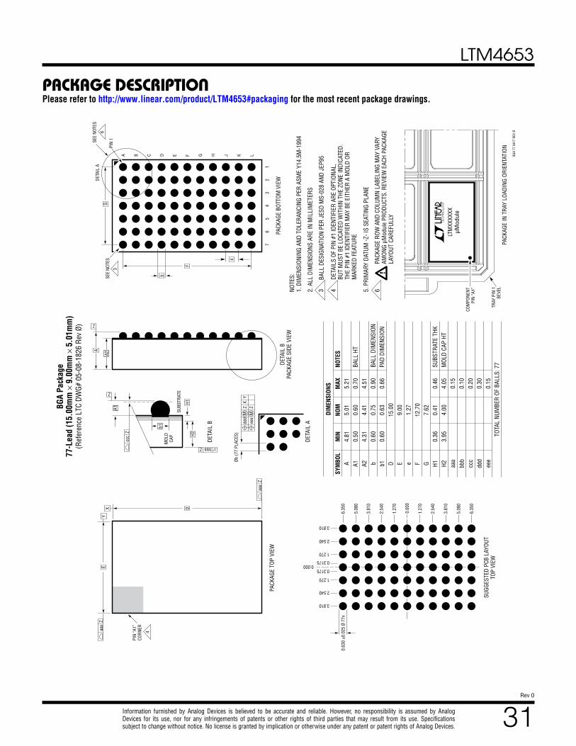
LTM4653
31Rev 0
For more information www.analog.com
PACKAGE DESCRIPTION
PACK
AGE
TOP
VIEW
4
PIN
“A1”
CORN
ER
YX
aaa
Z
aaa
Z
BGA
Pack
age
77-L
ead
(15.
00m
m ×
9.0
0mm
× 5
.01m
m)
(Ref
eren
ce L
TC D
WG#
05-
08-1
826
Rev
Ø)
NOTE
S:1.
DIM
ENSI
ONIN
G AN
D TO
LERA
NCIN
G PE
R AS
ME
Y14.
5M-1
994
2. A
LL D
IMEN
SION
S AR
E IN
MIL
LIM
ETER
S
BAL
L DE
SIGN
ATIO
N PE
R JE
SD M
S-02
8 AN
D JE
P95
43
DETA
ILS
OF P
IN #
1 ID
ENTI
FIER
ARE
OPT
IONA
L,BU
T M
UST
BE L
OCAT
ED W
ITHI
N TH
E ZO
NE IN
DICA
TED.
THE
PIN
#1 ID
ENTI
FIER
MAY
BE
EITH
ER A
MOL
D OR
M
ARKE
D FE
ATUR
E
DETA
IL A
Øb (7
7 PL
ACES
)
A
DETA
IL B
PACK
AGE
SIDE
VIE
W
MX
YZ
ddd
MZ
eee
A2
D
E
BGA
77 0
417
REV
Ø
TRAY
PIN
1BE
VEL
PACK
AGE
IN T
RAY
LOAD
ING
ORIE
NTAT
ION
COM
PONE
NTPI
N “A
1”
LTM
XXXX
XXµM
odul
e
DETA
IL A
PACK
AGE
BOTT
OM V
IEW
3
SEE
NOTE
S
A B C D E F G H J K L
PIN
1
e
b
F
G
76
54
32
1
SUGG
ESTE
D PC
B LA
YOUT
TOP
VIEW
0.00
0
2.54
0
3.81
0
5.08
0
6.35
0
1.27
0
3.81
0
2.54
0
1.27
0
5.08
0
6.35
0
3.810
2.540
1.270
3.810
2.540
1.270
0.3175
0.31750.000
0.63
0 ±0
.025
Ø 7
7x
6
SEE
NOTE
S
5. P
RIM
ARY
DATU
M -Z
- IS
SEAT
ING
PLAN
E
6PA
CKAG
E RO
W A
ND C
OLUM
N LA
BELI
NG M
AY V
ARY
AMON
G µM
odul
e PR
ODUC
TS. R
EVIE
W E
ACH
PACK
AGE
LAYO
UT C
AREF
ULLY
!
SYM
BOL
A A1 A2 b b1 D E e F G H1 H2 aaa
bbb
ccc
ddd
eee
MIN
4.81
0.50
4.31
0.60
0.60
0.36
3.95
NOM
5.01
0.60
4.41
0.75
0.63
15.0
09.
001.
2712
.70
7.62
0.41
4.00
MAX
5.21
0.70
4.51
0.90
0.66
0.46
4.05
0.15
0.10
0.20
0.30
0.15
TOTA
L NU
MBE
R OF
BAL
LS: 7
7
DIM
ENSI
ONS
NOTE
S
BALL
HT
BALL
DIM
ENSI
ONPA
D DI
MEN
SION
SUBS
TRAT
E TH
KM
OLD
CAP
HT
Z
DETA
IL B
SUBS
TRAT
E
A1
ccc
Z
Z
// bbb Z
H2H1
b1M
OLD
CAP
Please refer to http://www.linear.com/product/LTM4653#packaging for the most recent package drawings.
Information furnished by Analog Devices is believed to be accurate and reliable. However, no responsibility is assumed by Analog Devices for its use, nor for any infringements of patents or other rights of third parties that may result from its use. Specifications subject to change without notice. No license is granted by implication or otherwise under any patent or patent rights of Analog Devices.
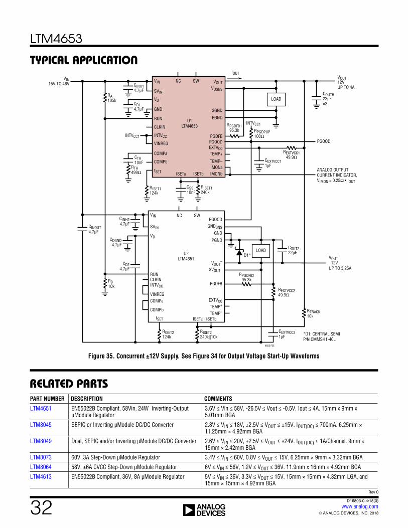
LTM4653
32Rev 0
For more information www.analog.com ANALOG DEVICES, INC. 2018
D16803-0-4/18(0) www.analog.com
RELATED PARTS
TYPICAL APPLICATION
Figure 35. Concurrent ±12V Supply. See Figure 34 for Output Voltage Start-Up Waveforms
VOUTVOSNS
SGND
PGND
PGDFB
IMONaIMONbISETbISETa
TEMP+
TEMP–
PGOODEXTVCC
INTVCC
fSET
COMPa
COMPb
CLKIN
RUN
GND
NC SW
VD
SVIN
VIN
VINREG
U1LTM4653
U2LTM4651
VOUT 12VUP TO 4A
RPGDFB195.3k RPGDPUP
100Ω
COUTH22µF×2
INTVCC1
IOUT
LOAD
PGOOD
ANALOG OUTPUTCURRENT INDICATOR,VIMON = 0.25Ω • IOUT
REXTVCC149.9Ω
CEXTVCC11µF
RfSET1124k
CTH10nF
RTH499Ω
RISET1240k
CSS10nF
CINH14.7μF
RA105k
CD14.7μF
INTVCC1
VIN15V TO 46V
CINOUT4.7µF
CINH24.7µF
CDGND4.7µF
CD24.7µF
RB10k
RfSET2124k
RISET2240k||10k
fSET
COMPb
COMPaVINREG
INTVCC
CLKINRUN
ISETa ISETb
VD
SVIN
VIN
VOUT–
SVOUT–
PGND
GND
PGDFB
4653 F35
PGOOD
D1*
*D1: CENTRAL SEMIP/N CMMSH1-40L
EXTVCC
GNDSNS
TEMP+
TEMP–
COUT222µFLOAD
REXTVCC249.9Ω
RTRACK10k
CEXTVCC21µF
VOUT–
–12VUP TO 3.25A
RPGDFB295.3k
NC SW
PART NUMBER DESCRIPTION COMMENTS
LTM4651 EN55022B Compliant, 58Vin, 24W Inverting-Output μModule Regulator
3.6V ≤ Vin ≤ 58V, -26.5V ≤ Vout ≤ -0.5V, Iout ≤ 4A. 15mm x 9mm x 5.01mm BGA
LTM8045 SEPIC or Inverting µModule DC/DC Converter 2.8V ≤ VIN ≤ 18V, ±2.5V ≤ VOUT ≤ ±15V. IOUT(DC) ≤ 700mA. 6.25mm × 11.25mm × 4.92mm BGA
LTM8049 Dual, SEPIC and/or Inverting µModule DC/DC Converter 2.6V ≤ VIN ≤ 20V, ±2.5V ≤ VOUT ≤ ±24V. IOUT(DC) ≤ 1A/Channel. 9mm × 15mm × 2.42mm BGA
LTM8073 60V, 3A Step-Down µModule Regulator 3.4V ≤ VIN ≤ 60V, 0.8V ≤ VOUT ≤ 15V. 6.25mm × 9mm × 3.32mm BGA
LTM8064 58V, ±6A CVCC Step-Down µModule Regulator 6V ≤ VIN ≤ 58V, 1.2V ≤ VOUT ≤ 36V. 11.9mm x 16mm × 4.92mm BGA
LTM4613 EN55022B Compliant, 36V, 8A µModule Regulator 5V ≤ VIN ≤ 36V, 3.3V ≤ VOUT ≤ 15V. 15mm × 15mm × 4.32mm LGA, and 15mm × 15mm × 4.92mm BGA