LTC6226/LTC6227 (Rev. 0) · 2020-03-06 · LTC6226/LTC6227 4 R 0 For more information SThe l...
28
LTC6226/LTC6227 1 Rev 0 For more information www.analog.com Document Feedback TYPICAL APPLICATION FEATURES DESCRIPTION 1nV/√ Hz 420MHz GBW, 180V/µs, Low Distortion Rail-to-Rail Output Op Amps The LTC ® 6226/LTC6227 are very fast, low noise rail-to-rail output, unity gain stable single/dual op amps, with a gain- bandwidth product of 420MHz and a slew rate of 180V/μs. The low input referred voltage noise of only 1nV/√Hz and low distortion of less than –90dB C for 4V P-P signals at 1MHz makes them ideal for applications that require high dynamic range and deal with very fast signals, such as driving A/D converters. The combination of low offset, low offset drift, high gain (139dB) and high CMRR (114dB) make these excellent devices for high dynamic range applications. The LTC6226 family maintains excellent performance for supply voltages of 2.8V to 11.75V and the devices are fully specified at supplies of 3V, 5V and 10V (±5V). With an input range extending to the negative rail and rail-to-rail output stage, the operational amplifier can accommodate wide swinging signals, and true single supply operation. For space constrained applications, the amplifiers come in 2mm × 2mm DFN (single) and 3mm × 3mm DFN (dual) packages. The devices are also available in 8-lead SOIC,TSOT-23 and MS8E. These amplifiers can be used as replacements for many high speed op amps to improve speed, noise and dynamic range. High Performance Transparent LTC6227 Based Driver for the 16-Bit AD7380 APPLICATIONS n Ultra Low Voltage Noise: 1nV/√Hz n Low Distortion: HD2/HD3<–90dB C at 4V P-P ,1MHz into 1kΩ n High Slew Rate: 180V/μs n GBW = 420MHz n –3dB Frequency (A V = +1): 330MHz n Input Common Mode Range Includes Negative Rail n Output Swings Rail-to-Rail n Supply Current: 5.5mA/Channel Typ n Operating Supply Range: 2.8V to 11.75V n Input Offset Voltage: 95μV Max n Offset Drift :0.4μV/°C n Low Power Shutdown n Very High Open Loop Gain: 9V/μV (139dB), R L = 1kΩ n Operating Temp Range: –40°C to 125°C n Single in 8-Lead SOIC, TSOT-23, 2mm × 2mm DFN. Duals in 3mm × 3mm DFN, MS8E n Optical Electronics: Fast AC-Coupled Transimpedance Amplifiers n Driving High Dynamic Range A/D Converters n Active Filters n Video Amplifiers n Low Voltage Low Distortion Amplification All registered trademarks and trademarks are the property of their respective owners. – + 330pF 3.3V 3.3V ADR4533 2.5V 2.2μF 1/2 LTC6227 33Ω 68pF 3.3V 0V 68pF 62267 TA01a – + 1/2 LTC6227 33Ω 5V –2.5V 3.3V 0V AD7380 IN – IN + V CC V REF V LOGIC 16-Bit ADC Driver Performance Input Signal = –0.5dBFS f SMPL = 4Msps, f IN = 50kHz 6.23V P–P 50kHz INPUT SIGNAL FREQUENCY (kHz) 0 400 800 1200 1600 2000 –180 –160 –140 –120 –100 –80 –60 –40 –20 0 AMPLITUDE (dBFS) LTC62277 TA01b SNR = 91 dB THD = –104.8 dB SFDR = 108.5 dB
Transcript of LTC6226/LTC6227 (Rev. 0) · 2020-03-06 · LTC6226/LTC6227 4 R 0 For more information SThe l...
LTC6226/LTC6227
1Rev 0
For more information www.analog.comDocument Feedback
TYPICAL APPLICATION
FEATURES DESCRIPTION
1nV/√Hz 420MHz GBW, 180V/µs, Low Distortion Rail-to-Rail Output Op Amps
The LTC®6226/LTC6227 are very fast, low noise rail-to-rail output, unity gain stable single/dual op amps, with a gain-bandwidth product of 420MHz and a slew rate of 180V/μs. The low input referred voltage noise of only 1nV/√Hz and low distortion of less than –90dBC for 4VP-P signals at 1MHz makes them ideal for applications that require high dynamic range and deal with very fast signals, such as driving A/D converters.
The combination of low offset, low offset drift, high gain (139dB) and high CMRR (114dB) make these excellent devices for high dynamic range applications.
The LTC6226 family maintains excellent performance for supply voltages of 2.8V to 11.75V and the devices are fully specified at supplies of 3V, 5V and 10V (±5V).
With an input range extending to the negative rail and rail-to-rail output stage, the operational amplifier can accommodate wide swinging signals, and true single supply operation.
For space constrained applications, the amplifiers come in 2mm × 2mm DFN (single) and 3mm × 3mm DFN (dual) packages. The devices are also available in 8-lead SOIC,TSOT-23 and MS8E.
These amplifiers can be used as replacements for many high speed op amps to improve speed, noise and dynamic range.
High Performance Transparent LTC6227 Based Driver for the 16-Bit AD7380
APPLICATIONS
n Ultra Low Voltage Noise: 1nV/√Hz n Low Distortion: HD2/HD3<–90dBC at 4VP-P,1MHz
into 1kΩ n High Slew Rate: 180V/μs n GBW = 420MHz n –3dB Frequency (AV = +1): 330MHz n Input Common Mode Range Includes Negative Rail n Output Swings Rail-to-Rail n Supply Current: 5.5mA/Channel Typ n Operating Supply Range: 2.8V to 11.75V n Input Offset Voltage: 95μV Max n Offset Drift :0.4μV/°C n Low Power Shutdown n Very High Open Loop Gain: 9V/μV (139dB), RL = 1kΩ n Operating Temp Range: –40°C to 125°C n Single in 8-Lead SOIC, TSOT-23, 2mm × 2mm DFN.
Duals in 3mm × 3mm DFN, MS8E
n Optical Electronics: Fast AC-Coupled Transimpedance Amplifiers
n Driving High Dynamic Range A/D Converters n Active Filters n Video Amplifiers n Low Voltage Low Distortion Amplification
All registered trademarks and trademarks are the property of their respective owners.
–
+
330pF
3.3V
3.3V
ADR4533
2.5V 2.2µF
1/2 LTC622733Ω
68pF3.3V
0V
68pF
62267 TA01a
–
+1/2 LTC6227
33Ω
5V
–2.5V
3.3V
0V
AD7380
IN–
IN+ VCC VREF VLOGIC
16-Bit ADC Driver PerformanceInput Signal = –0.5dBFSfSMPL = 4Msps, fIN = 50kHz
6.23VP–P 50kHz INPUT SIGNAL
FREQUENCY (kHz)0 400 800 1200 1600 2000
–180
–160
–140
–120
–100
–80
–60
–40
–20
0
AMPL
ITUD
E (d
BFS)
LTC62277 TA01b
SNR = 91 dBTHD = –104.8 dBSFDR = 108.5 dB
LTC6226/LTC6227
2Rev 0
For more information www.analog.com
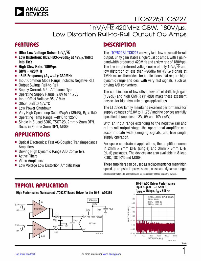
ABSOLUTE MAXIMUM RATINGSTotal Supply Voltage (V– to V+) .................................12VInput Voltage (–IN, +IN, SHDN)....V– – 0.3V to V+ + 0.3VInput Current (–IN, +IN, SHDN) (Note 2) .............. ±10mAOperating Temperature Range
LTC6226I/LTC6227I (Note 4) ...............–40°C to 85°C LTC6226H/LTC6227H (Note 4) .......... –40°C to 125°C
Specified Temperature Range LTC6226I/LTC6227I (Note 4) ...............–40°C to 85°C LTC6226H/LTC6227H (Note 4) .......... –40°C to 125°C
Output Current (Note 3) ..................................... ±100mAOutput Short-Circuit Duration .............Thermally LimitedStorage Temperature Range .................. –65°C to 125°CMaximum Junction Temperature .......................... 150°CMSOP Lead Temperature (Soldering 10s) ............. 300°C
(Note 1)
1
2
3
4
8
7
6
5
TOP VIEW
SHDN
V+
OUT
V–
FB
–IN
+IN
V–
S8 PACKAGE8-LEAD PLASTIC SO
+–
TJMAX = 150°C, θJA = 120°C/W (NOTE 8)
1
2
3
6
5
4
TOP VIEW
S6 PACKAGE6-LEAD PLASTIC TSOT-23
V+
SHDN
–IN
OUT
V–
+IN+ –
TJMAX = 150°C, θJA = 192°C/W (NOTE 8)
TOP VIEW
OUT
–IN
SHDN
V+
+IN
V–
DC PACKAGE6-LEAD (2mm × 2mm) PLASTIC DFN
4
57V–
6
3
2
1
TJMAX = 150°C, θJA = 80°C/W (NOTE 8)
EXPOSED PAD (PIN 7) IS V–, MUST BE SOLDERED TO PCB
1234
OUTA–INA+INA
V–
8765
V+
OUTB–INB+INB
TOP VIEW
MSE PACKAGE8-LEAD PLASTIC MSOP
+–+
–
9V–
TJMAX = 150°C, θJA = 35°C/W (NOTE 8)
EXPOSED PAD (PIN 9) IS V–, MUST BE SOLDERED TO PCB
TOP VIEW
11V–
DD PACKAGE10-LEAD (3mm × 3mm) PLASTIC DFN
10
9
6
7
8
4
5
3
2
1 V+
OUTB
–INB
+INB
SHDNB
OUTA
–INA
+INA
V–
SHDNA
TJMAX = 125°C, θJA = 43°C/W (NOTE 8)
EXPOSED PAD (PIN 11) IS V–, MUST BE SOLDERED TO PCB
PIN CONFIGURATION
LTC6226/LTC6227
3Rev 0
For more information www.analog.com
The l denotes the specifications which apply over the full operating temperature range, otherwise specifications are at TA = 25°C. VS = ±5V,VCM = 0V, VSHDN = floating unless otherwise noted.
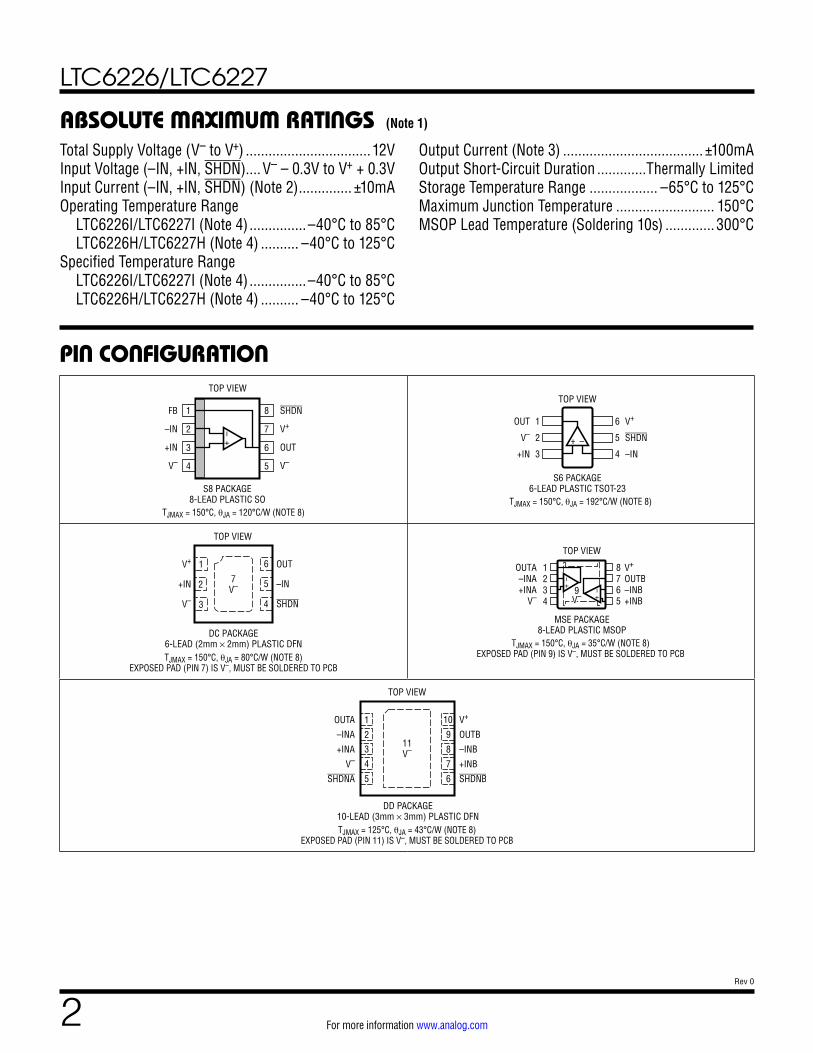
ORDER INFORMATION
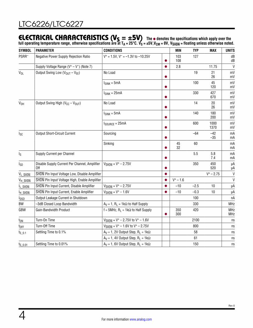
ELECTRICAL CHARACTERISTICS (VS = ±5V)
SYMBOL PARAMETER CONDITIONS MIN TYP MAX UNITS
VOS Input Offset Voltage
l
–95 –225
20 95 225
μV μV
ΔVOS Input Offset Voltage Match (Channel to Channel, LTC6227, Note 5)
l
–140 –400
18 140 400
μV μV
TCVOS Input Offset Voltage Drift l 0.4 μV/°C
IB Input Bias Current (Note 6)
l
–20 –25
–8.4 μA μA
ΔIB Input Bias Current Match (Channel to Channel,LTC6227, Note 5)
l
–2 –3
0.3 2 3
µA µA
IOS Input Offset Current
l
–0.35 –0.5
0.2 0.35 0.5
μA µA
ΔIOS Input OffsetCurrent Match (Channel to Channel, LTC6227, Note 5)
l
–0.7 –1
0.15 0.7 1
µA µA
en Input Noise Voltage Spectral Density f = 1MHz 1 nV/√Hz
Integrated 1/f Noise 0.1Hz to 10Hz 0.77 μVP-P
in Input Noise Current Spectral Density f = 1MHz 2.4 pA/√Hz
CIN Input Capacitance Differential Mode Common Mode
3 1
pF pF
RIN Input Resistance Differential Mode Common Mode
4.7 6
kΩ MΩ
AVOL Large Signal Voltage Gain RL = 1kΩ to Half Supply VOUT = ±4V
l
114 110
139 dB dB
RL = 100Ω to Half Supply VOUT = ±2.5V
l
93 88
110 dB dB
CMRR Common Mode Rejection Ratio VCM = V– – 0.1V to V+ – 1.2V
l
100 95
114 dB dB
VCMR Input Common Mode Range (Note 10) l V–– 0.1 V+ – 1.2 V
PSRR+ Positive Power Supply Rejection Ratio V– = –1V, V+ = 1.8V to 10.75V
l
100 95
115 dB dB
LEAD FREE FINISH TAPE AND REEL PART MARKING PACKAGE DESCRIPTION TEMPERATURE RANGE
LTC6226IS6#TRMPBF LTC6226IS6#TRPBF LTHGY 6-Lead TSOT-23 –40°C to 85°C
LTC6226HS6#TRMPBF LTC6226HS6#TRPBF LTHGY 6-Lead TSOT-23 –40ºC to 125°C
LTC6226IDC#TRMPBF LTC6226IDC#TRPBF LHGZ 6-Lead 2mm × 2mm DFN –40°C to 85°C
LTC6226HDC#TRMPBF LTC6226HDC#TRPBF LHGZ 6-Lead 2mm × 2mm DFN –40ºC to 125°C
LTC6226IS8#PBF LTC6226IS8#TRPBF 6226 8-Lead SOIC-8 –40°C to 85°C
LTC6226HS8#PBF LTC6226HS8#TRPBF 6226 8-Lead SOIC-8 –40ºC to 125°C
LTC6227IMS8E#PBF LTC6227IMS8E#TRPBF LTHHB 8-Lead MSOP, Exposed Pad –40°C to 85°C
LTC6227HMS8E#PBF LTC6227HMS8E#TRPBF LTHHB 8-Lead MSOP, Exposed Pad –40ºC to 125°C
LTC6227IDD#PBF LTC6227IDD#TRPBF LHHC 10-Lead 3mm × 3mm DFN –40°C to 85°C
LTC6227HDD#PBF LTC6227HDD#TRPBF LHHC 10-Lead 3mm × 3mm DFN –40ºC to 125°C
Contact the factory for parts specified with wider operating temperature ranges.
Tape and reel specifications. Some packages are available in 500 unit reels through designated sales channels with #TRMPBF suffix.
LTC6226/LTC6227
4Rev 0
For more information www.analog.com
The l denotes the specifications which apply over the full operating temperature range, otherwise specifications are at TA = 25°C. VS = ±5V,VCM = 0V, VSHDN = floating unless otherwise noted.ELECTRICAL CHARACTERISTICS (VS = ±5V)
SYMBOL PARAMETER CONDITIONS MIN TYP MAX UNITS
PSRR– Negative Power Supply Rejection Ratio V+ = 1.5V, V– = –1.3V to –10.25V
l
103 108
127 dB dB
Supply Voltage Range (V+ – V–) (Note 7) l 2.8 11.75 V
VOL Output Swing Low (VOUT – VEE) No Load
l
19 21 26
mV mV
ISINK = 5mA
l
100 45 120
mV mV
ISINK = 25mA
l
330 427 670
mV mV
VOH Output Swing High (VCC – VOUT) No Load
l
14 20 26
mV mV
ISINK = 5mA
l
140 180 200
mV mV
ISOURCE = 25mA
l
600 1000 1370
mV mV
ISC Output Short-Circuit Current Sourcing
l
–64 –42 –35
mA mA
Sinking
l
45 32
60 mA mA
IS Supply Current per Channel
l
5.5 5.8 7.4
mA mA
ISD Disable Supply Current Per Channel, Amplifier Off
VSHDN = V+ – 2.75V
l
350 450 520
μA μA
VL_SHDN SHDN Pin Input Voltage Low, Disable Amplifier l V+ – 2.75 V
VH_SHDN SHDN Pin Input Voltage High, Enable Amplifier l V+ – 1.6 V
IL_SHDN SHDN Pin Input Current, Disable Amplifier VSHDN = V+ – 2.75V l –10 –2.5 10 μA
IH_SHDN SHDN Pin Input Current, Enable Amplifier VSHDN = V+ – 1.6V l –10 –0.3 10 μA
IOSD Output Leakage Current in Shutdown 100 nA
BW –3dB Closed Loop Bandwidth AV = 1, RL = 1kΩ to Half Supply 330 MHz
GBW Gain-Bandwidth Product f = 5MHz, RL = 1kΩ to Half Supply
l
350 300
420 MHz MHz
tON Turn-On Time VSHDN = V+ – 2.75V to V+ – 1.6V 2100 ns
tOFF Turn-Off Time VSHDN = V+ – 1.6V to V+ – 2.75V 800 ns
tS_0.1 Settling Time to 0.1% AV = 1, 2V Output Step, RL = 1kΩ 58 ns
AV = 1, 4V Output Step, RL = 1kΩ 61 ns
tS_0.01 Settling Time to 0.01% AV = 1, 6V Output Step, RL = 1kΩ 150 ns
LTC6226/LTC6227
5Rev 0
For more information www.analog.com
The l denotes the specifications which apply over the full operating temperature range, otherwise specifications are at TA = 25°C. VS = ±5V,VCM = 0V, VSHDN = floating unless otherwise noted.
The l denotes the specifications which apply over the full operating temperature range, otherwise specifications are at TA = 25°C. VS = 5V, 0V,VCM = VOUT = 2.5V, VSHDN = floating unless otherwise noted.
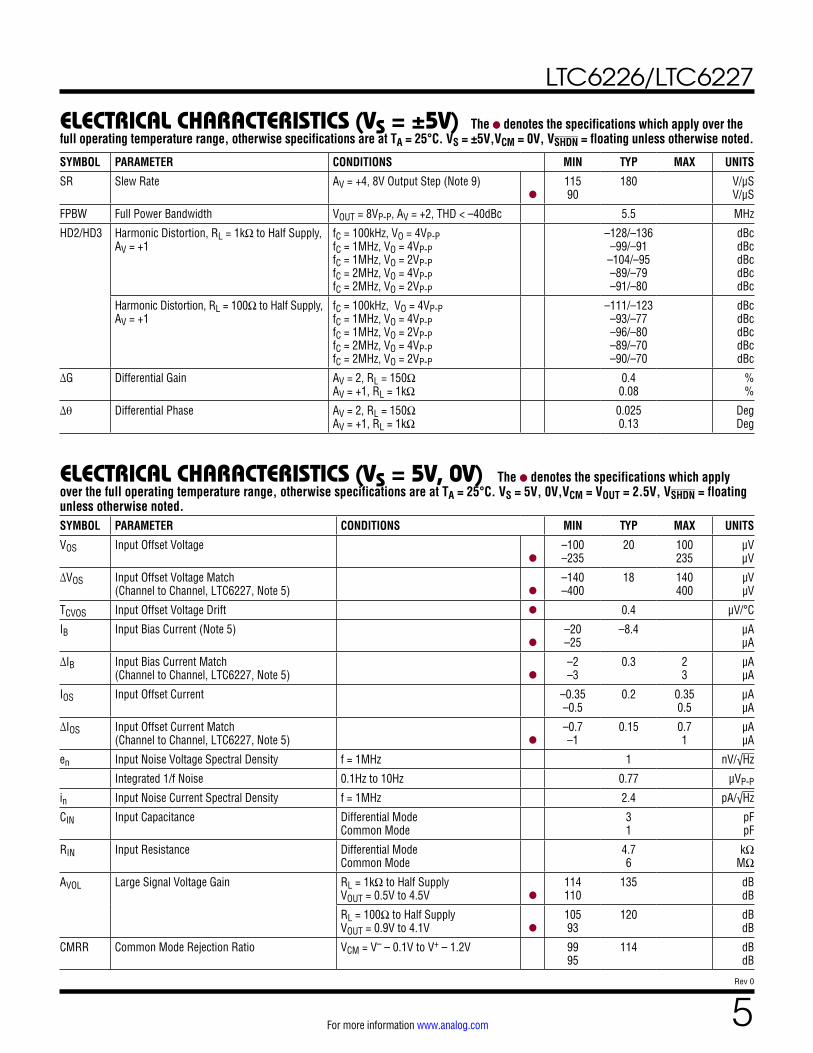
ELECTRICAL CHARACTERISTICS (VS = ±5V)
ELECTRICAL CHARACTERISTICS (VS = 5V, 0V)
SYMBOL PARAMETER CONDITIONS MIN TYP MAX UNITS
SR Slew Rate AV = +4, 8V Output Step (Note 9)
l
115 90
180 V/μS V/μS
FPBW Full Power Bandwidth VOUT = 8VP-P, AV = +2, THD < –40dBc 5.5 MHz
HD2/HD3 Harmonic Distortion, RL = 1kΩ to Half Supply, AV = +1
fC = 100kHz, VO = 4VP-P fC = 1MHz, VO = 4VP-P fC = 1MHz, VO = 2VP-P fC = 2MHz, VO = 4VP-P fC = 2MHz, VO = 2VP-P
–128/–136 –99/–91
–104/–95 –89/–79 –91/–80
dBc dBc dBc dBc dBc
Harmonic Distortion, RL = 100Ω to Half Supply, AV = +1
fC = 100kHz, VO = 4VP-P fC = 1MHz, VO = 4VP-P fC = 1MHz, VO = 2VP-P fC = 2MHz, VO = 4VP-P fC = 2MHz, VO = 2VP-P
–111/–123 –93/–77 –96/–80 –89/–70 –90/–70
dBc dBc dBc dBc dBc
ΔG Differential Gain AV = 2, RL = 150Ω AV = +1, RL = 1kΩ
0.4 0.08
% %
Δθ Differential Phase AV = 2, RL = 150Ω AV = +1, RL = 1kΩ
0.025 0.13
Deg Deg
SYMBOL PARAMETER CONDITIONS MIN TYP MAX UNITS
VOS Input Offset Voltage
l
–100 –235
20 100 235
μV μV
ΔVOS Input Offset Voltage Match (Channel to Channel, LTC6227, Note 5)
l
–140 –400
18 140 400
µV µV
TCVOS Input Offset Voltage Drift l 0.4 μV/°C
IB Input Bias Current (Note 5)
l
–20 –25
–8.4 μA μA
ΔIB Input Bias Current Match (Channel to Channel, LTC6227, Note 5)
l
–2 –3
0.3 2 3
µA µA
IOS Input Offset Current –0.35 –0.5
0.2 0.35 0.5
μA µA
ΔIOS Input Offset Current Match (Channel to Channel, LTC6227, Note 5)
l
–0.7 –1
0.15 0.7 1
µA µA
en Input Noise Voltage Spectral Density f = 1MHz 1 nV/√Hz
Integrated 1/f Noise 0.1Hz to 10Hz 0.77 μVP-P
in Input Noise Current Spectral Density f = 1MHz 2.4 pA/√Hz
CIN Input Capacitance Differential Mode Common Mode
3 1
pF pF
RIN Input Resistance Differential Mode Common Mode
4.7 6
kΩ MΩ
AVOL Large Signal Voltage Gain RL = 1kΩ to Half Supply VOUT = 0.5V to 4.5V
l
114 110
135 dB dB
RL = 100Ω to Half Supply VOUT = 0.9V to 4.1V
l
105 93
120 dB dB
CMRR Common Mode Rejection Ratio VCM = V– – 0.1V to V+ – 1.2V 99 95
114 dB dB
LTC6226/LTC6227
6Rev 0
For more information www.analog.com
The l denotes the specifications which apply over the full operating temperature range, otherwise specifications are at TA = 25°C. VS = 5V, 0V,VCM = VOUT = 2.5V, VSHDN = floating unless otherwise noted.
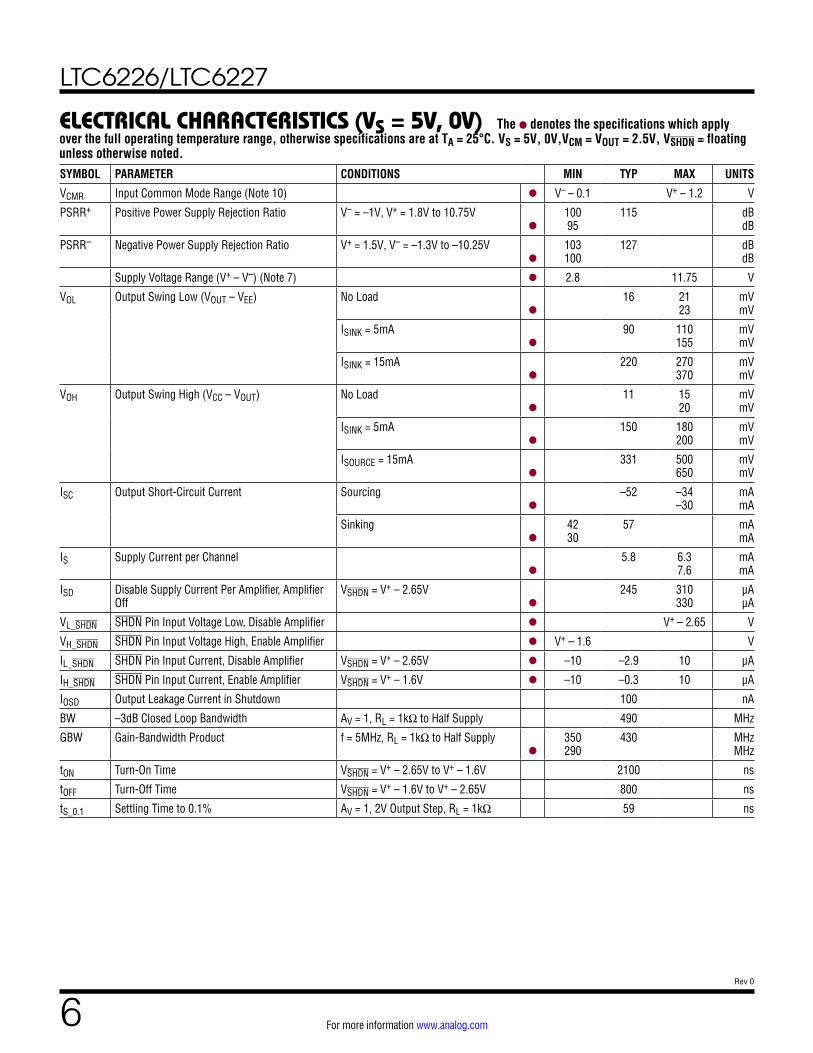
ELECTRICAL CHARACTERISTICS (VS = 5V, 0V)
SYMBOL PARAMETER CONDITIONS MIN TYP MAX UNITS
VCMR Input Common Mode Range (Note 10) l V– – 0.1 V+ – 1.2 V
PSRR+ Positive Power Supply Rejection Ratio V– = –1V, V+ = 1.8V to 10.75V
l
100 95
115 dB dB
PSRR– Negative Power Supply Rejection Ratio V+ = 1.5V, V– = –1.3V to –10.25V
l
103 100
127 dB dB
Supply Voltage Range (V+ – V–) (Note 7) l 2.8 11.75 V
VOL Output Swing Low (VOUT – VEE) No Load
l
16 21 23
mV mV
ISINK = 5mA
l
90 110 155
mV mV
ISINK = 15mA
l
220 270 370
mV mV
VOH Output Swing High (VCC – VOUT) No Load
l
11 15 20
mV mV
ISINK = 5mA
l
150 180 200
mV mV
ISOURCE = 15mA
l
331 500 650
mV mV
ISC Output Short-Circuit Current Sourcing
l
–52 –34 –30
mA mA
Sinking
l
42 30
57 mA mA
IS Supply Current per Channel
l
5.8 6.3 7.6
mA mA
ISD Disable Supply Current Per Amplifier, Amplifier Off
VSHDN = V+ – 2.65V
l
245 310 330
μA μA
VL_SHDN SHDN Pin Input Voltage Low, Disable Amplifier l V+ – 2.65 V
VH_SHDN SHDN Pin Input Voltage High, Enable Amplifier l V+ – 1.6 V
IL_SHDN SHDN Pin Input Current, Disable Amplifier VSHDN = V+ – 2.65V l –10 –2.9 10 μA
IH_SHDN SHDN Pin Input Current, Enable Amplifier VSHDN = V+ – 1.6V l –10 –0.3 10 μA
IOSD Output Leakage Current in Shutdown 100 nA
BW –3dB Closed Loop Bandwidth AV = 1, RL = 1kΩ to Half Supply 490 MHz
GBW Gain-Bandwidth Product f = 5MHz, RL = 1kΩ to Half Supply
l
350 290
430 MHz MHz
tON Turn-On Time VSHDN = V+ – 2.65V to V+ – 1.6V 2100 ns
tOFF Turn-Off Time VSHDN = V+ – 1.6V to V+ – 2.65V 800 ns
tS_0.1 Settling Time to 0.1% AV = 1, 2V Output Step, RL = 1kΩ 59 ns
LTC6226/LTC6227
7Rev 0
For more information www.analog.com
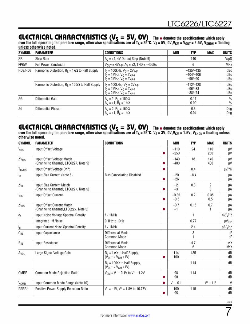
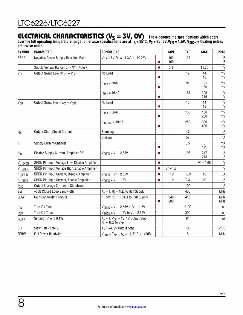
The l denotes the specifications which apply over the full operating temperature range, otherwise specifications are at TA = 25°C. VS = 3V, 0V,VCM = 1.5V, VSHDN = floating unless otherwise noted.
ELECTRICAL CHARACTERISTICS (VS = 3V, 0V)
SYMBOL PARAMETER CONDITIONS MIN TYP MAX UNITS
VOS Input Offset Voltage
l
–110 –250
24 110 250
μV μV
ΔVOS Input Offset Voltage Match (Channel to Channel, LTC6227, Note 5)
l
–140 –400
18 140 400
µV µV
TCVOS Input Offset Voltage Drift l 0.4 μV/°C
IB Input Bias Current (Note 6) Bias Cancellation Disabled
l
–20 –26
–8.4 μA μA
ΔIB Input Bias Current Match (Channel to Channel, LTC6227, Note 5)
l
–2 –3
0.3 2 3
µA µA
IOS Input Offset Current
l
–0.35 –0.5
0.2 0.35 0.5
μA µA
ΔIOS Input Offset Current Match (Channel to Channel,LTC6227, Note 5)
l
–0.7 –1
0.15 0.7 1
μA µA
en Input Noise Voltage Spectral Density f = 1MHz 1 nV/√Hz
Integrated 1/f Noise 0.1Hz to 10Hz 0.77 μVP-P
in Input Current Noise Spectral Density f = 1MHz 2.4 pA/√Hz
CIN Input Capacitance Differential Mode Common Mode
3 1
pF pF
RIN Input Resistance Differential Mode Common Mode
4.7 6
kΩ MΩ
AVOL Large Signal Voltage Gain RL = 1kΩ to Half Supply, (VOUT = VCM ±1V)
l
114 100
135 dB dB
RL = 100Ω to Half Supply, (VOUT = VCM ±1V)
114 dB
CMRR Common Mode Rejection Ratio VCM = V– – 0.1V to V+ – 1.2V
l
98 90
114 dB dB
VCMR Input Common Mode Range (Note 10) l V– – 0.1 V+ – 1.2 V
PSRR+ Positive Power Supply Rejection Ratio V– = –1V, V+ = 1.8V to 10.75V
l
100 95
115 dB dB
The l denotes the specifications which apply over the full operating temperature range, otherwise specifications are at TA = 25°C. VS = 5V, 0V,VCM = VOUT = 2.5V, VSHDN = floating unless otherwise noted.
ELECTRICAL CHARACTERISTICS (VS = 5V, 0V)
SYMBOL PARAMETER CONDITIONS MIN TYP MAX UNITS
SR Slew Rate AV = +4, 4V Output Step (Note 9) 140 V/μS
FPBW Full Power Bandwidth VOUT = 4VP-P, AV = +2, THD < –40dBc 6 MHz
HD2/HD3 Harmonic Distortion, RL = 1kΩ to Half Supply fC = 100kHz, VO = 2VP-P fC = 1MHz, VO = 2VP-P fC = 2MHz, VO = 2VP-P
–125/–135 –104/–106 –90/–90
dBc dBc dBc
Harmonic Distortion, RL = 100Ω to Half Supply fC = 100kHz, VO = 2VP-P fC = 1MHz, VO = 2VP-P fC = 2MHz, VO = 2VP-P
–112/–128 –96/–88 –88/–74
dBc dBc dBc
ΔG Differential Gain AV = 2, RL = 150Ω AV = +1, RL = 1kΩ
0.17 0.09
% %
Δθ Differential Phase AV = 2, RL = 150Ω AV = +1, RL = 1kΩ
0.3 0.04
Deg Deg
LTC6226/LTC6227
8Rev 0
For more information www.analog.com
The l denotes the specifications which apply over the full operating temperature range, otherwise specifications are at TA = 25°C. VS = 3V, 0V,VCM = 1.5V, VSHDN = floating unless otherwise noted.
ELECTRICAL CHARACTERISTICS (VS = 3V, 0V)
SYMBOL PARAMETER CONDITIONS MIN TYP MAX UNITS
PSRR– Negative Power Supply Rejection Ratio V+ = 1.5V, V– = –1.3V to –10.25V
l
103 100
127 dB dB
Supply Voltage Range (V+ – V–) (Note 7) l 2.8 11.75 V
VOL Output Swing Low (VOUT – VEE) No Load
l
12 14 18
mV mV
ISINK = 5mA
l
91 121 160
mV mV
ISINK = 10mA
l
161 205 275
mV mV
VOH Output Swing High (VCC – VOUT) No Load
l
10 14 18
mV mV
ISINK = 5mA
l
150 180 230
mV mV
ISOURCE = 10mA
l
250 330 430
mV mV
ISC Output Short Circuit Current Sourcing 47 mA
Sinking 57 mA
IS Supply Current/Channel
l
5.5 6 7.25
mA mA
ISD Disable Supply Current, Amplifier Off VSHDN = V+ – 2.65V l 195 247 278
μA µA
VL_SHDN SHDN Pin Input Voltage Low, Disable Amplifier l V+ – 2.65 V
VH_SHDN SHDN Pin Input Voltage High, Enable Amplifier l V+ – 1.6 V
IL_SHDN SHDN Pin Input Current, Disable Amplifier VSHDN = V+ – 2.65V l –10 –2.9 10 μA
IH_SHDN SHDN Pin Input Current, Enable Amplifier VSHDN = V+ – 1.6V l –10 0.3 10 μA
IOSD Output Leakage Current in Shutdown 100 nA
BW –3dB Closed Loop Bandwidth AV = 1, RL = 1kΩ to Half Supply 450 MHz
GBW Gain-Bandwidth Product f = 5MHz, RL = 1kΩ to Half Supply
l
340 280
415 MHz MHz
tON Turn-On Time VSHDN = V+ – 2.65V to V+ – 1.6V 2100 ns
tOFF Turn-Off Time VSHDN = V+ – 1.6V to V+ – 2.65V 800 ns
tS_0.1 Settling Time to 0.1% AV = 1, VCM = 1V, 1V Output Step, RL = 1kΩ to VCM
84 ns
SR Slew Rate (Note 9) AV = +4, 2V Output Step 100 V/μS
FPBW Full Power Bandwidth VOUT = 2VP-P, AV = –1, THD < –40dBc 8 MHz
LTC6226/LTC6227
9Rev 0
For more information www.analog.com
The l denotes the specifications which apply over the full operating temperature range, otherwise specifications are at TA = 25°C. VS = 3V, 0V,VCM = 1.5V, VSHDN = floating unless otherwise noted.
ELECTRICAL CHARACTERISTICS (VS = 3V, 0V)
Note 1: Stresses beyond those listed under Absolute Maximum Ratings may cause permanent damage to the device. Exposure to any Absolute Maximum Rating condition for extended periods may affect device reliability and lifetime.Note 2: The inputs are protected by back-to-back diodes. If any of the input or shutdown pins goes 300mV beyond either supply or the differential input voltage exceeds 0.7V, the input current should be limited to less than 10mA.Note 3: A heat sink may be required to keep the junction temperature below the absolute maximum rating when the output current is high.Note 4: The LTC6226I/LTC6227I are guaranteed functional and specified over the temperature range of –40°C to 85°C. The LTC6226H/LTC6227H are guaranteed and specified functional over the temperature range of –40°C to 125°C.
Note 5: Matching parameters are the difference between amplifiers A and B on the LTC6227.Note 6: The input bias current is the average of the average of the currents through the positive and negative input pins.Note 7: Supply Voltage Range is guaranteed by Power Supply Rejection Ratio test.Note 8: Thermal resistance varies with the amount of PC board metal connected to the package. The specified values are with short traces connected to the leads.Note 9: Middle 2/3 of the output waveform is observed for Slew Rate. RL = 1k to half supply.Note 10: Input Common Mode Range is guaranteed by Common Mode Rejection Ratio Test.
SYMBOL PARAMETER CONDITIONS MIN TYP MAX UNITS
HD2/HD3 Harmonic Distortion, RL = 1kΩ to VCM, VOUT = 1VP-P, VCM = 1V
fC = 100kHz fC = 1MHz fC = 2MHz
–122/–137 –108/–111 –95/–95
dBc dBc dBc
Harmonic Distortion, RL = 100Ω to VCM, VOUT = 1VP-P, VCM = 1V
fC = 100kHz fC = 1MHz fC = 2MHz
–113/–130 –100/–94 –90/–79
dBc dBc dBc
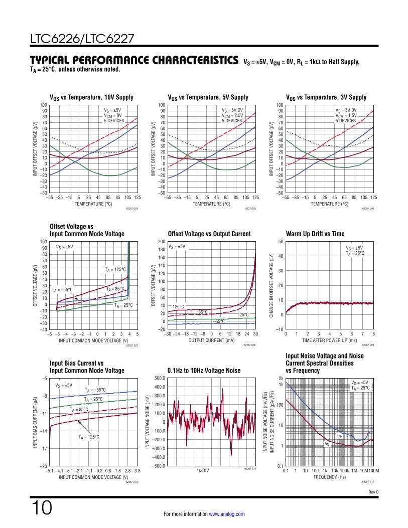
TYPICAL PERFORMANCE CHARACTERISTICS
Offset Distribution Offset Distribution Offset Distribution
VS = ±5V, VCM = 0V, RL = 1kΩ to Half Supply, TA = 25°C, unless otherwise noted.
VS = ±5VVCM = 0V T300 UNITS
A = 25°C
INPUT OFFSET VOLTAGE (µV)–50 –40 –30 –20 –10 0 10 20 30 40 50
0
5
10
15
20
25
30
35
40
45
50
PERC
ENT
OF U
NITS
(%)
62267 G01
VS = 5V, 0VVCM = 2.5V TA = 25°C
INPUT OFFSET VOLTAGE (µV)–50 –40 –30 –20 –10 0 10 20 30 40 50
0
5
10
15
20
25
30
35
40
45
50
PERC
ENT
OF U
NITS
(%)
62267 G02
300 UNITS
VS = 3V, 0VVCM = 1.5V TA = 25°C
INPUT OFFSET VOLTAGE (µV)–50 –40 –30 –20 –10 0 10 20 30 40 50
0
5
10
15
20
25
30
35
40
45
50
PERC
ENT
OF U
NITS
(%)
62267 G03
300 UNITS
LTC6226/LTC6227
10Rev 0
For more information www.analog.com
TYPICAL PERFORMANCE CHARACTERISTICS
VOS vs Temperature, 10V Supply VOS vs Temperature, 5V Supply VOS vs Temperature, 3V Supply
VS = ±5V, VCM = 0V, RL = 1kΩ to Half Supply, TA = 25°C, unless otherwise noted.
Offset Voltage vs Input Common Mode Voltage Offset Voltage vs Output Current Warm Up Drift vs Time
Input Bias Current vs Input Common Mode Voltage 0.1Hz to 10Hz Voltage Noise
Input Noise Voltage and Noise Current Spectral Densities vs Frequency
VS = ±5VVCM = 0V5 DEVICES
TEMPERATURE (°C)–55 –35 –15 5 25 45 65 85 105 125
–50–40–30–20–10
0102030405060708090
100
INPU
T OF
FSET
VOL
TAGE
(µV)
62267 G04
VS = 5V, 0VVCM = 2.5V5 DEVICES
TEMPERATURE (°C)–55 –35 –15 5 25 45 65 85 105 125
–50–40–30–20–10
0102030405060708090
100
INPU
T OF
FSET
VOL
TAGE
(µV)
6227 G05
VS = 3V, 0VVCM = 1.5V5 DEVICES
TEMPERATURE (°C)–55 –35 –15 5 25 45 65 85 105 125
–50–40–30–20–10
0102030405060708090
100
INPU
T OF
FSET
VOL
TAGE
(µV)
62267 G06
TA = 125°C
TA = 25°C
TA = –55°C
VS = ±5V
TA = 85°C
INPUT COMMON MODE VOLTAGE (V)–6 –5 –4 –3 –2 –1 0 1 2 3 4 5
–40–30–20–10
0102030405060708090
100
OFFS
ET V
OLTA
GE (µ
V)
62267 G07
125°C
25°C–55°C
VS = ±5V
85°C
OUTPUT CURRENT (mA)–30 –24 –18 –12 –6 0 6 12 18 24 30
–20
0
20
40
60
80
100
120
140
160
180
200
OFFS
ET V
OLTA
GE (µ
V)
62267 G08
VS = ±5VTA = 25°C
TIME AFTER POWER UP (ms)0 1 2 3 4 5 6 7 8
–10
0
10
20
30
40
50
CHAN
GE IN
OFF
SET
VOLT
AGE
(µV)
62267 G09
VS = ±5VTA = –55°C
TA = 25°C
TA = 85°C
TA = 125°C
INPUT COMMON MODE VOLTAGE (V)–5.1 –4.1 –3.1 –2.1 –1.1 –0.2 0.8 1.8 2.8 3.8
–20
–17
–14
–11
–8
–5
INPU
T BI
AS C
URRE
NT (µ
A)
62267 G10
1s/DIV–500.0
–400.0
–300.0
–200.0
–100.0
0
100.0
200.0
300.0
400.0
500.0
INPU
T VO
LTAG
E NO
ISE
( nV)
62267 G11
VS = ±5VTA = 25°C
eN
iN,
FREQUENCY (Hz)0.1 1 10 100 1k 10k 100k 1M 10M100M
0.1
1
10
100
1k2k
INPU
T NO
ISE
CURR
ENT
(pA/
√Hz)
INPU
T NO
ISE
VOLT
AGE
(nV/
√Hz)
62267 G12
LTC6226/LTC6227
11Rev 0
For more information www.analog.com
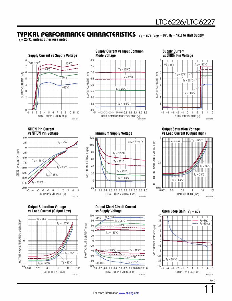
TYPICAL PERFORMANCE CHARACTERISTICS VS = ±5V, VCM = 0V, RL = 1kΩ to Half Supply, TA = 25°C, unless otherwise noted.
Supply Current vs Supply VoltageSupply Current vs Input Common Mode Voltage
Supply Current vs SHDN Pin Voltage
SHDN Pin Current vs SHDN Pin Voltage Minimum Supply Voltage
VCM = VS/2 125°C
25°C
–55°C
85°C
TOTAL SUPPLY VOLTAGE (V)0 1 2 3 4 5 6 7 8 9 10 11 12
0
1
2
3
4
5
6
7
8
SUPP
LY C
URRE
NT (m
A)
62267 G13
TA = 125°C
TA = 25°C
TA = –55°C
TA = 85°C
INPUT COMMON MODE VOLTAGE (V)–5.1 –4.2 –3.3 –2.4 –1.5 –0.6 0.3 1.2 2.1 3.0 3.9
4.0
4.5
5.0
5.5
6.0
6.5
7.0
7.5
8.0
SUPP
LY C
URRE
NT (m
A)
62267 G014
VS = ±5V TA = 125°C
TA = 25°C
TA = –55°C
TA = 85°C
SHDN PIN VOLTAGE (V)–5 –4 –3 –2 –1 0 1 2 3 4 5
0
1
2
3
4
5
6
7
8
SUPP
LY C
URRE
NT (m
A)
62267 G14
VS = ±5V
TA = –55°C
TA = 125°C
TA = 25°C
TA = –85°C
SHDN PIN VOLTAGE (V)–5 –4 –3 –2 –1 0 1 2 3 4 5
–20.0
–17.5
–15.0
–12.5
–10.0
–7.5
–5.0
–2.5
0
2.5
5.0
SHDN
PIN
CUR
RENT
(µA)
62267 G16
TA = 125°C
TA = 85°C
TA = 25°C
TA = –55°C
VCM = VEE+1V
TOTAL SUPPLY VOLTAGE (V)2 2.2 2.4 2.6 2.8 3.0 3.2 3.4 3.6 3.8 4.0
–20
0
20
40
60
80
100
120
INPU
T OF
FSET
VOL
TAGE
(µV)
62267 G17
Output Saturation Voltage vs Load Current (Output High)
Output Saturation Voltage vs Load Current (Output Low)
Output Short Circuit Current vs Supply Voltage
TA = 125°C
TA = –55°C
TA = 25°C
VS = ±5V
TA = 85°C
LOAD CURRENT (mA)0.001 0.01 0.1 1 10 100
0.01
0.1
1
OUTP
UT H
IGH
SATU
RATI
ON V
OLTA
GE (V
)
62267 G18
TA = 125°C
TA = –55°C TA = 25°C
VS = ±5V
TA = 85°C
LOAD CURRENT (mA)0.001 0.01 0.1 1 10 100
0.01
0.1
1
OUTP
UT H
IGH
SATU
RATI
ON V
OLTA
GE (V
)
62267 G19
SOURCE
SINK TA = –55°C
TA = –55°C
TA = 25°C
TA = 25°C
TA = 125°C
TA = 125°C
TA = 85°C
TA = 85°C
TOTAL SUPPLY VOLTAGE (V)2.8 3.7 4.6 5.5 6.4 7.3 8.2 9.1 10.0 10.9 11.8
–100
–80
–60
–40
–20
0
20
40
60
80
100
SHOR
T CI
RCUI
T CU
RREN
T (m
A)
62267 G20
Open Loop Gain, VS = ±5V
TA = 25 °C
RL=1kΩRL=100Ω
OUTPUT VOLTAGE (V)–5 –4 –3 –2 –1 0 1 2 3 4 5
–40
–32
–24
–16
–8
0
8
16
24
32
40
INPU
T OF
FSET
VOL
TAGE
(µV)
62267 G21
LTC6226/LTC6227
12Rev 0
For more information www.analog.com
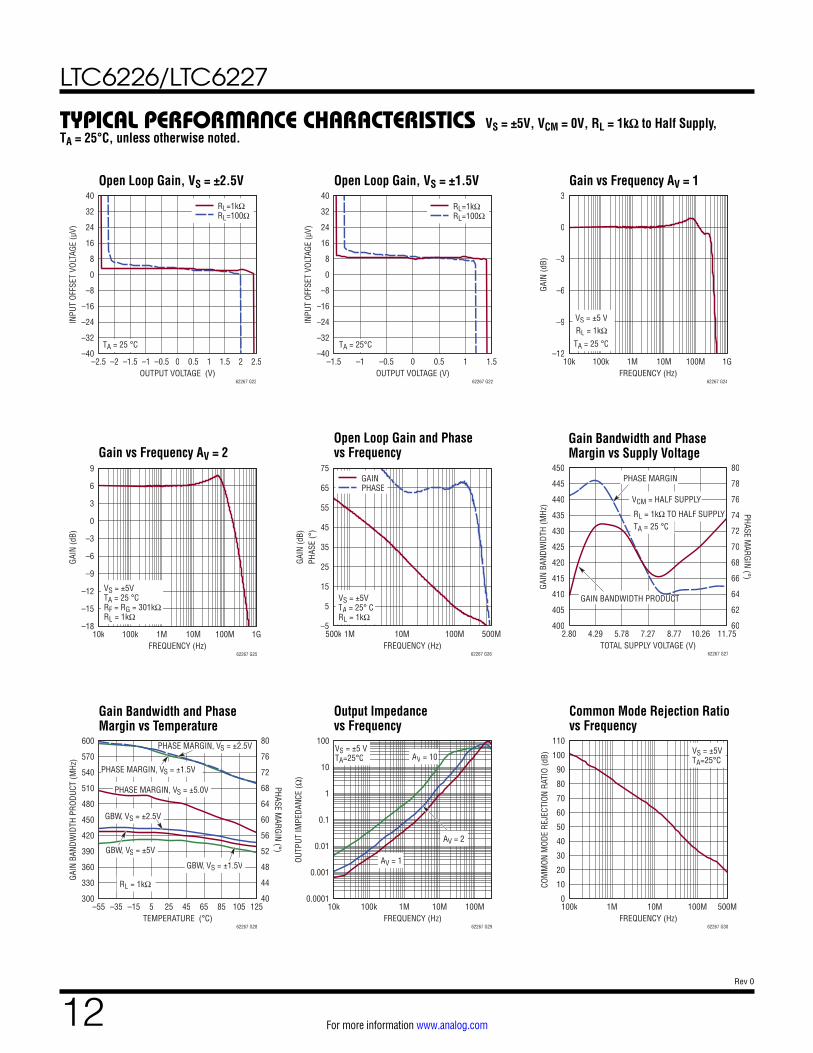
TYPICAL PERFORMANCE CHARACTERISTICS VS = ±5V, VCM = 0V, RL = 1kΩ to Half Supply, TA = 25°C, unless otherwise noted.
Open Loop Gain, VS = ±2.5V Open Loop Gain, VS = ±1.5V Gain vs Frequency AV = 1
Gain vs Frequency AV = 2Open Loop Gain and Phase vs Frequency
Gain Bandwidth and Phase Margin vs Supply Voltage
Gain Bandwidth and Phase Margin vs Temperature
Output Impedance vs Frequency
Common Mode Rejection Ratio vs Frequency
TA = 25 °C
RL=1kΩRL=100Ω
OUTPUT VOLTAGE (V)–2.5 –2 –1.5 –1 –0.5 0 0.5 1 1.5 2 2.5
–40
–32
–24
–16
–8
0
8
16
24
32
40
INPU
T OF
FSET
VOL
TAGE
(µV)
62267 G22
TA = 25°C
RL=1kΩRL=100Ω
OUTPUT VOLTAGE (V)–1.5 –1 –0.5 0 0.5 1 1.5
–40
–32
–24
–16
–8
0
8
16
24
32
40
INPU
T OF
FSET
VOL
TAGE
(µV)
62267 G22
VS = ±5 VRL = 1kΩ
TA = 25 °C
FREQUENCY (Hz)10k 100k 1M 10M 100M 1G
–12
–9
–6
–3
0
3
GAIN
(dB)
62267 G24
VS = ±5V TA = 25 °CRF = RG = 301kΩ RL = 1kΩ
FREQUENCY (Hz)10k 100k 1M 10M 100M 1G
–18
–15
–12
–9
–6
–3
0
3
6
9
GAIN
(dB)
62267 G25
VS = ±5V TA = 25° C RL = 1kΩ
GAINPHASE
FREQUENCY (Hz)500k 1M 10M 100M 500M
–5
5
15
25
35
45
55
65
75
PHAS
E (°
)GA
IN (d
B)
62267 G26
TA = 25 °CRL = 1kΩ TO HALF SUPPLY
VCM = HALF SUPPLY
GAIN BANDWIDTH PRODUCT
PHASE MARGIN
TOTAL SUPPLY VOLTAGE (V)2.80 4.29 5.78 7.27 8.77 10.26 11.75
400
405
410
415
420
425
430
435
440
445
450
60
62
64
66
68
70
72
74
76
78
80
GAIN
BAN
DWID
TH (M
Hz)
PHASE MARGIN (°)
62267 G27
RL = 1kΩ
GBW, VS = ±5V
GBW, VS = ±2.5V
PHASE MARGIN, VS = ±2.5V
GBW, VS = ±1.5V
PHASE MARGIN, VS = ±1.5V
PHASE MARGIN, VS = ±5.0V
TEMPERATURE (°C)–55 –35 –15 5 25 45 65 85 105 125
300
330
360
390
420
450
480
510
540
570
600
40
44
48
52
56
60
64
68
72
76
80
GAIN
BAN
DWID
TH P
RODU
CT (M
Hz)
PHASE MARGIN (°)
62267 G28
VS = ±5 VTA=25°C
AV = 1
AV = 10
AV = 2
FREQUENCY (Hz)10k 100k 1M 10M 100M
0.0001
0.001
0.01
0.1
1
10
100
OUTP
UT IM
PEDA
NCE
(Ω)
62267 G29
VS = ±5VTA=25°C
FREQUENCY (Hz)100k 1M 10M 100M 500M0
10
20
30
40
50
60
70
80
90
100
110
COM
MON
MOD
E RE
JECT
ION
RATI
O (d
B)
62267 G30
LTC6226/LTC6227
13Rev 0
For more information www.analog.com
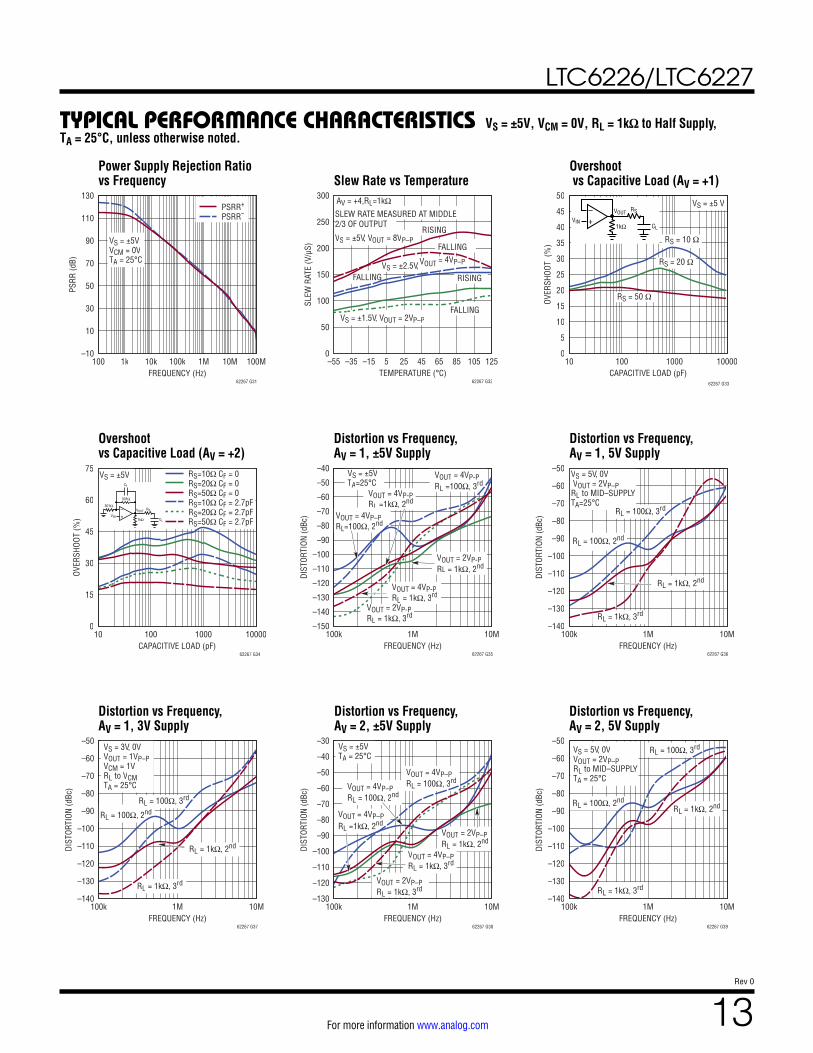
TYPICAL PERFORMANCE CHARACTERISTICS VS = ±5V, VCM = 0V, RL = 1kΩ to Half Supply, TA = 25°C, unless otherwise noted.
Power Supply Rejection Ratio vs Frequency Slew Rate vs Temperature
Overshoot vs Capacitive Load (AV = +1)
Overshoot vs Capacitive Load (AV = +2)
Distortion vs Frequency, AV = 1, ±5V Supply
Distortion vs Frequency, AV = 1, 5V Supply
VS = ±5VVCM = 0VTA = 25°C
PSRR+
PSRR–
FREQUENCY (Hz)100 1k 10k 100k 1M 10M 100M
–10
10
30
50
70
90
110
130
PSRR
(dB)
62267 G31
AV = +4,RL=1kΩ
SLEW RATE MEASURED AT MIDDLE 2/3 OF OUTPUT
RISING
FALLING RISING
FALLINGVS = ±5V, VOUT = 8VP–P
VS = ±2.5V,VOUT = 4VP–P
VS = ±1.5V, VOUT = 2VP–PFALLING
TEMPERATURE (°C)–55 –35 –15 5 25 45 65 85 105 125
0
50
100
150
200
250
300
SLEW
RAT
E (V
/µS)
62267 G32
RS = 20 Ω
RS = 50 Ω
RS = 10 Ω
VS = ±5 V
CAPACITIVE LOAD (pF)10 100 1000 10000
0
5
10
15
20
25
30
35
40
45
50
OVER
SHOO
T (%
)
62267 G33
+–
VOUT
1kΩVIN
RS
CL
VS = ±5V RS=10Ω CF = 0RS=20Ω CF = 0RS=50Ω CF = 0RS=10Ω CF = 2.7pFRS=20Ω CF = 2.7pFRS=50Ω CF = 2.7pF
CAPACITIVE LOAD (pF)10 100 1000 10000
0
15
30
45
60
75
OVER
SHOO
T (%
)
62267 G34
+–
VOUT
1kΩ
301Ω
301Ω
VIN
RS
CF
CL
VS = ±5VTA=25°C
VOUT = 4VP-P RL =1kΩ, 2nd
VOUT = 4VP-P RL = 1kΩ, 3rd
VOUT = 2VP-P RL = 1kΩ, 3rd
VOUT = 2VP-P RL = 1kΩ, 2nd
VOUT = 4VP-P RL =100Ω, 3rd
VOUT = 4VP–P RL =100Ω, 2nd
FREQUENCY (Hz)100k 1M 10M
–150
–140
–130
–120
–110
–100
–90
–80
–70
–60
–50
–40
DIST
ORTI
ON (d
Bc)
62267 G35
VS = 5V, 0V VOUT = 2VP–PRL to MID–SUPPLY TA=25°C
RL = 1kΩ, 2nd
RL = 100Ω, 2nd
RL = 1kΩ, 3rd
RL = 100Ω, 3rd
FREQUENCY (Hz)100k 1M 10M
–140
–130
–120
–110
–100
–90
–80
–70
–60
–50
DIST
ORTI
ON (d
Bc)
62267 G36
Distortion vs Frequency, AV = 1, 3V Supply
Distortion vs Frequency, AV = 2, ±5V Supply
Distortion vs Frequency, AV = 2, 5V Supply
RL = 100Ω, 2nd
VS = 3V, 0V VOUT = 1VP–PVCM = 1V RL to VCM TA = 25°C
RL = 1kΩ, 2nd
RL = 1kΩ, 3rd
RL = 100Ω, 3rd
FREQUENCY (Hz)100k 1M 10M
–140
–130
–120
–110
–100
–90
–80
–70
–60
–50
DIST
ORTI
ON (d
Bc)
62267 G37
VS = ±5VTA = 25°C
VOUT = 4VP–P RL = 100Ω, 3rd
VOUT = 4VP–P RL = 100Ω, 2nd
VOUT = 4VP–P RL =1kΩ, 2nd
VOUT = 4VP–P RL = 1kΩ, 3rd
VOUT = 2VP–P RL = 1kΩ, 3rd
VOUT = 2VP–P RL = 1kΩ, 2nd
FREQUENCY (Hz)100k 1M 10M
–130
–120
–110
–100
–90
–80
–70
–60
–50
–40
–30
DIST
ORTI
ON (d
Bc)
62267 G38
VS = 5V, 0V VOUT = 2VP–PRL to MID–SUPPLY TA = 25°C
RL = 1kΩ, 2nd RL = 100Ω, 2nd
RL = 1kΩ, 3rd
RL = 100Ω, 3rd
FREQUENCY (Hz)100k 1M 10M
–140
–130
–120
–110
–100
–90
–80
–70
–60
–50
DIST
ORTI
ON (d
Bc)
62267 G39
LTC6226/LTC6227
14Rev 0
For more information www.analog.com
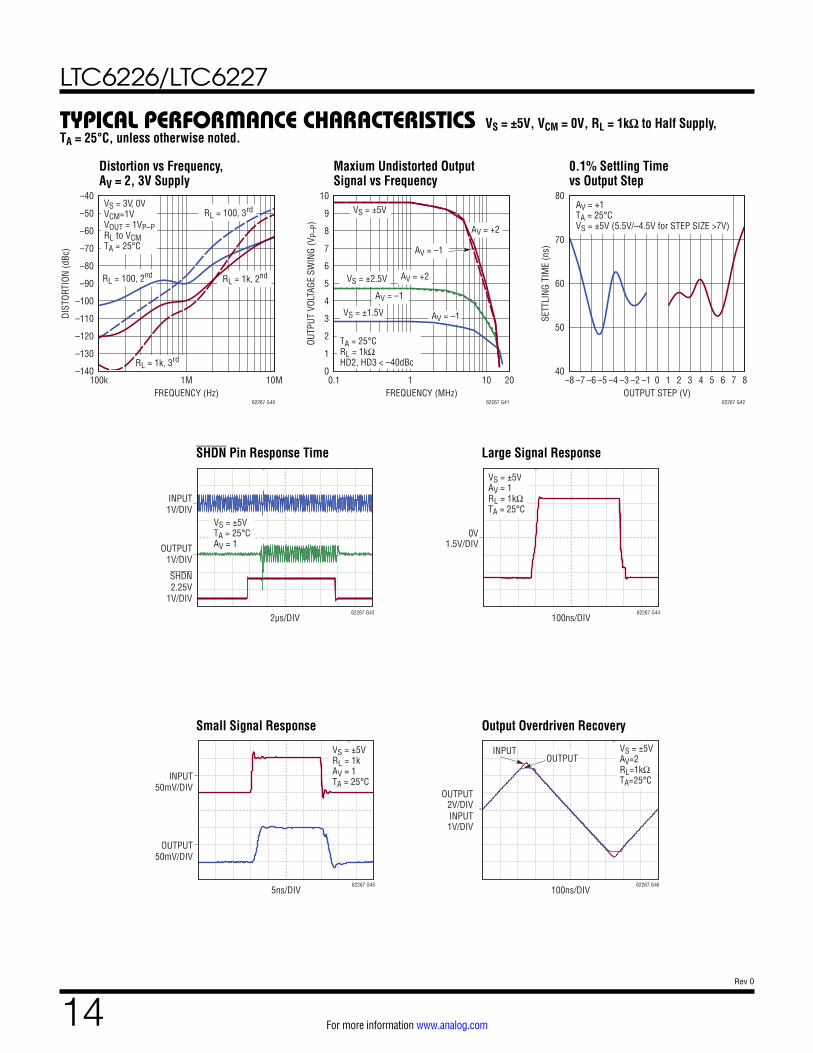
TYPICAL PERFORMANCE CHARACTERISTICS VS = ±5V, VCM = 0V, RL = 1kΩ to Half Supply, TA = 25°C, unless otherwise noted.
Distortion vs Frequency, AV = 2, 3V Supply
Maxium Undistorted Output Signal vs Frequency
0.1% Settling Time vs Output Step
SHDN Pin Response Time Large Signal Response
Small Signal Response Output Overdriven Recovery
VS = 3V, 0VVCM=1VVOUT = 1VP–PRL to VCMTA = 25°C
RL = 100, 2nd RL = 1k, 2nd
RL = 1k, 3rd
RL = 100, 3rd
FREQUENCY (Hz)100k 1M 10M
–140
–130
–120
–110
–100
–90
–80
–70
–60
–50
–40
DIST
ORTI
ON (d
Bc)
62267 G40
VS = ±5V
VS = ±2.5V
VS = ±1.5V
AV = +2
AV = –1
AV = –1
AV = +2
AV = –1
TA = 25°CRL = 1kΩHD2, HD3 < –40dBc
FREQUENCY (MHz)0.1 1 10 20
0
1
2
3
4
5
6
7
8
9
10
OUTP
UT V
OLTA
GE S
WIN
G (V
P–P)
62267 G41
AV = +1TA = 25°CVS = ±5V (5.5V/–4.5V for STEP SIZE >7V)
OUTPUT STEP (V)–8 –7 –6 –5 –4 –3 –2 –1 0 1 2 3 4 5 6 7 8
40
50
60
70
80
SETT
LING
TIM
E (n
s)
62267 G42
VS = ±5VTA = 25°CAV = 1
INPUT1V/DIV
OUTPUT1V/DIV
SHDN2.25V
1V/DIV
2µs/DIV62267 G43
VS = ±5VAV = 1RL = 1kΩTA = 25°C
100ns/DIV
0V1.5V/DIV
62267 G44
VS = ±5VRL = 1kAV = 1TA = 25°CINPUT
50mV/DIV
OUTPUT50mV/DIV
5ns/DIV62267 G45
VS = ±5VAV=2RL=1kΩTA=25°C
OUTPUTINPUT
100ns/DIV
INPUT1V/DIV
OUTPUT2V/DIV
62267 G46
LTC6226/LTC6227
15Rev 0
For more information www.analog.com
PIN FUNCTIONSFB (SOIC-8 Only): Feedback Pin. Internally connected to OUT.
+IN: Non-Inverting Input of Amplifier. Valid input range is from V– to V+ – 1.2V
–IN: Inverting Input of Amplifier. Valid input range is from V– to V+ – 1.2V
OUT: Output of the Amplifier. Swings rail to rail and can typically source/sink 60mA of current.
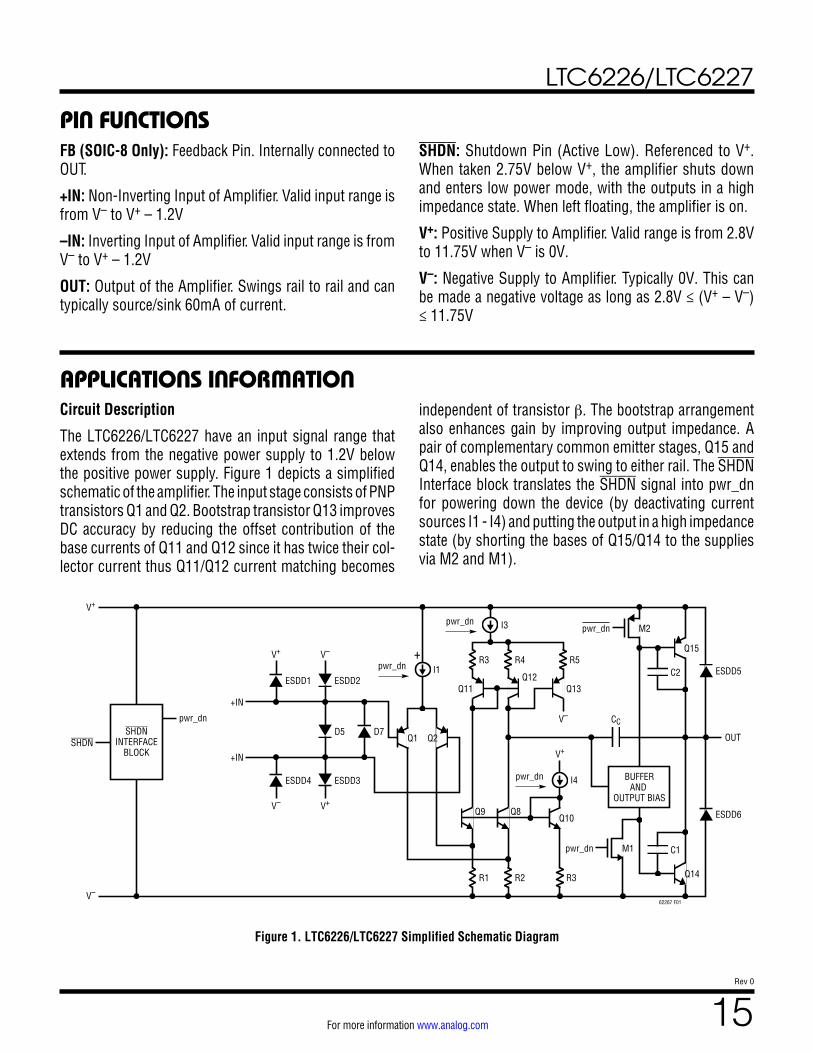
Circuit Description
The LTC6226/LTC6227 have an input signal range that extends from the negative power supply to 1.2V below the positive power supply. Figure 1 depicts a simplified schematic of the amplifier. The input stage consists of PNP transistors Q1 and Q2. Bootstrap transistor Q13 improves DC accuracy by reducing the offset contribution of the base currents of Q11 and Q12 since it has twice their col-lector current thus Q11/Q12 current matching becomes
SHDN: Shutdown Pin (Active Low). Referenced to V+. When taken 2.75V below V+, the amplifier shuts down and enters low power mode, with the outputs in a high impedance state. When left floating, the amplifier is on.
V+: Positive Supply to Amplifier. Valid range is from 2.8V to 11.75V when V– is 0V.
V–: Negative Supply to Amplifier. Typically 0V. This can be made a negative voltage as long as 2.8V ≤ (V+ – V–) ≤ 11.75V
independent of transistor β. The bootstrap arrangement also enhances gain by improving output impedance. A pair of complementary common emitter stages, Q15 and Q14, enables the output to swing to either rail. The SHDN Interface block translates the SHDN signal into pwr_dn for powering down the device (by deactivating current sources I1 - I4) and putting the output in a high impedance state (by shorting the bases of Q15/Q14 to the supplies via M2 and M1).
APPLICATIONS INFORMATION
Figure 1. LTC6226/LTC6227 Simplified Schematic Diagram
SHDN
62267 F01
V+
V–
V+
CCV–
V–
Q15
Q2
Q11
Q1
+IN
ESDD1
SHDNINTERFACE
BLOCK
pwr_dn
I1+
pwr_dn
I4pwr_dn
I3pwr_dn
pwr_dn
+IN
ESDD4
ESDD6
ESDD5
OUT
V+
V+ V–
ESDD3
ESDD2
D5 D7
R1 R2 R3
R3 R4 R5
M1 C1
Q10Q9 Q8
Q14
Q13Q12
BUFFERAND
OUTPUT BIAS
C2
M2pwr_dn
LTC6226/LTC6227
16Rev 0
For more information www.analog.com
APPLICATIONS INFORMATIONOutput
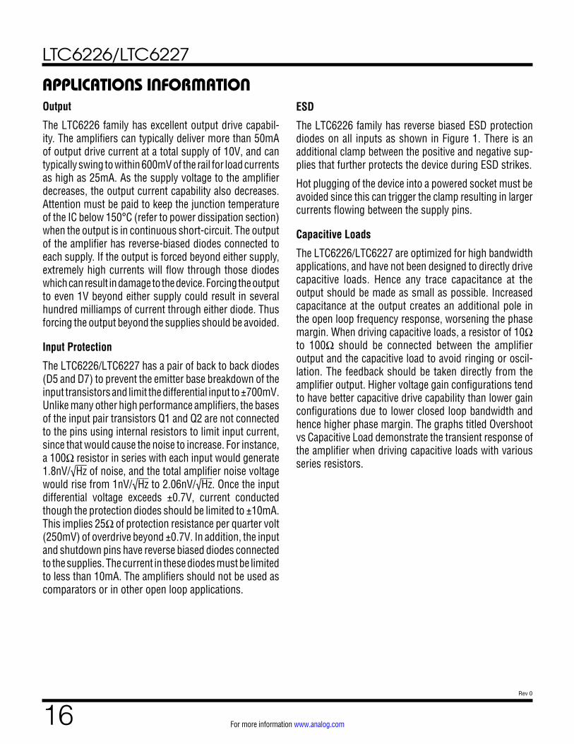
The LTC6226 family has excellent output drive capabil-ity. The amplifiers can typically deliver more than 50mA of output drive current at a total supply of 10V, and can typically swing to within 600mV of the rail for load currents as high as 25mA. As the supply voltage to the amplifier decreases, the output current capability also decreases. Attention must be paid to keep the junction temperature of the IC below 150°C (refer to power dissipation section) when the output is in continuous short-circuit. The output of the amplifier has reverse-biased diodes connected to each supply. If the output is forced beyond either supply, extremely high currents will flow through those diodes which can result in damage to the device. Forcing the output to even 1V beyond either supply could result in several hundred milliamps of current through either diode. Thus forcing the output beyond the supplies should be avoided.
Input Protection
The LTC6226/LTC6227 has a pair of back to back diodes (D5 and D7) to prevent the emitter base breakdown of the input transistors and limit the differential input to ±700mV. Unlike many other high performance amplifiers, the bases of the input pair transistors Q1 and Q2 are not connected to the pins using internal resistors to limit input current, since that would cause the noise to increase. For instance, a 100Ω resistor in series with each input would generate 1.8nV/√Hz of noise, and the total amplifier noise voltage would rise from 1nV/√Hz to 2.06nV/√Hz. Once the input differential voltage exceeds ±0.7V, current conducted though the protection diodes should be limited to ±10mA. This implies 25Ω of protection resistance per quarter volt (250mV) of overdrive beyond ±0.7V. In addition, the input and shutdown pins have reverse biased diodes connected to the supplies. The current in these diodes must be limited to less than 10mA. The amplifiers should not be used as comparators or in other open loop applications.
ESD
The LTC6226 family has reverse biased ESD protection diodes on all inputs as shown in Figure 1. There is an additional clamp between the positive and negative sup-plies that further protects the device during ESD strikes.
Hot plugging of the device into a powered socket must be avoided since this can trigger the clamp resulting in larger currents flowing between the supply pins.
Capacitive Loads
The LTC6226/LTC6227 are optimized for high bandwidth applications, and have not been designed to directly drive capacitive loads. Hence any trace capacitance at the output should be made as small as possible. Increased capacitance at the output creates an additional pole in the open loop frequency response, worsening the phase margin. When driving capacitive loads, a resistor of 10Ω to 100Ω should be connected between the amplifier output and the capacitive load to avoid ringing or oscil-lation. The feedback should be taken directly from the amplifier output. Higher voltage gain configurations tend to have better capacitive drive capability than lower gain configurations due to lower closed loop bandwidth and hence higher phase margin. The graphs titled Overshoot vs Capacitive Load demonstrate the transient response of the amplifier when driving capacitive loads with various series resistors.
LTC6226/LTC6227
17Rev 0
For more information www.analog.com
APPLICATIONS INFORMATION
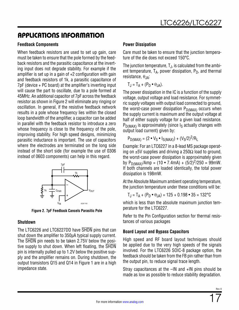
Figure 2. 7pF Feedback Cancels Parasitic Pole
Feedback Components
When feedback resistors are used to set up gain, care must be taken to ensure that the pole formed by the feed-back resistors and the parasitic capacitance at the invert-ing input does not degrade stability. For example if the amplifier is set up in a gain of +2 configuration with gain and feedback resistors of 1k, a parasitic capacitance of 7pF (device + PC board) at the amplifier’s inverting input will cause the part to oscillate, due to a pole formed at 45MHz. An additional capacitor of 7pF across the feedback resistor as shown in Figure 2 will eliminate any ringing or oscillation. In general, if the resistive feedback network results in a pole whose frequency lies within the closed loop bandwidth of the amplifier, a capacitor can be added in parallel with the feedback resistor to introduce a zero whose frequency is close to the frequency of the pole, improving stability. For high speed designs, minimizing parasitic inductance is important. The use of capacitors where the electrodes are terminated on the long side instead of the short side (for example the use of 0306 instead of 0603 components) can help in this regard.
Power Dissipation
Care must be taken to ensure that the junction tempera-ture of the die does not exceed 150°C.
The junction temperature, TJ, is calculated from the ambi-ent temperature, TA, power dissipation, PD, and thermal resistance, θJA:
TJ = TA + (PD • θJA).
The power dissipation in the IC is a function of the supply voltage, output voltage and load resistance. For symmet-ric supply voltages with output load connected to ground, the worst-case power dissipation PD(MAX) occurs when the supply current is maximum and the output voltage at half of either supply voltage for a given load resistance. PD(MAX) is approximately (since IS actually changes with output load current) given by:
PD(MAX) = (2 • VS • IS(MAX)) + (VS/2)2/RL
Example: For an LTC6227 in a 8-lead MS package operat-ing on ±5V supplies and driving a 250Ω load to ground, the worst-case power dissipation is approximately given by PD(MAX)/Amp = (10 • 7.4mA) + (5/2)2/250 = 99mW. If both channels are loaded identically, the total power dissipation is 198mW.
At the Absolute Maximum ambient operating temperature, the junction temperature under these conditions will be:
TJ = TA + (PD • θJA) = 125 + 0.198 • 35 = 132°C
which is less than the absolute maximum junction tem-perature for the LTC6227.
Refer to the Pin Configuration section for thermal resis-tances of various packages
Board Layout and Bypass Capacitors
High speed and RF board layout techniques should be applied due to the very high speeds of the signals involved. For the LTC6226 SOIC-8 package option, the feedback should be taken from the FB pin rather than from the output pin, to reduce signal trace length.
Stray capacitances at the –IN and +IN pins should be made as low as possible to reduce stability degradation.
Shutdown
The LTC6226 and LTC6227DD have SHDN pins that can shut down the amplifier to 350µA typical supply current. The SHDN pin needs to be taken 2.75V below the posi-tive supply to shut down. When left floating, the SHDN pin is internally pulled up to 1.2V below the positive sup-ply and the amplifier remains on. During shutdown, the output transistors Q15 and Q14 in Figure 1 are in a high impedance state.
62267 F02
7pF
1k
1k
CPAR
VIN
VOUT
–
+
LTC6226/LTC6227
18Rev 0
For more information www.analog.com
APPLICATIONS INFORMATION
Figure 3.
For single supply applications, it is recommended that high quality 0.1µF||1000pF ceramic bypass capacitors be placed directly between each V+ pin and its closest V– pin with short connections. The V– pins (including the Exposed Pad) should be tied directly to a low impedance ground plane with minimal routing. For dual (split) power supplies, it is recommended that additional high quality 0.1µF||1000pF ceramic capacitors be used to bypass V+ pins to ground and V– pins to ground, again with minimal routing.
Noise Considerations
The ultralow input referred voltage noise of of 1nV/√Hz is equivalent to that of an 60Ω resistor. As with all BJT input amplifiers, lowering input referred noise is achieved by increasing the collector current of the input differential pair, which increases the input referred current noise.
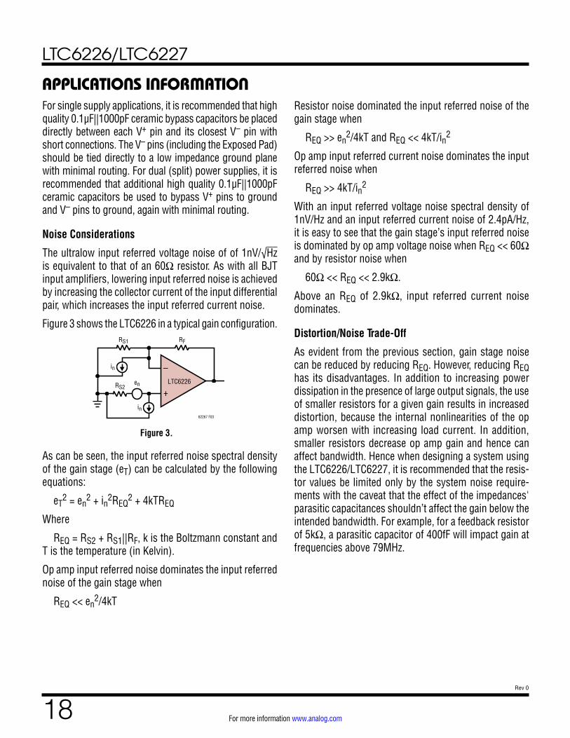
Figure 3 shows the LTC6226 in a typical gain configuration.
Resistor noise dominated the input referred noise of the gain stage when
REQ >> en2/4kT and REQ << 4kT/in2
Op amp input referred current noise dominates the input referred noise when
REQ >> 4kT/in2
With an input referred voltage noise spectral density of 1nV/Hz and an input referred current noise of 2.4pA/Hz, it is easy to see that the gain stage’s input referred noise is dominated by op amp voltage noise when REQ << 60Ω and by resistor noise when
60Ω << REQ << 2.9kΩ.
Above an REQ of 2.9kΩ, input referred current noise dominates.
Distortion/Noise Trade-Off
As evident from the previous section, gain stage noise can be reduced by reducing REQ. However, reducing REQ has its disadvantages. In addition to increasing power dissipation in the presence of large output signals, the use of smaller resistors for a given gain results in increased distortion, because the internal nonlinearities of the op amp worsen with increasing load current. In addition, smaller resistors decrease op amp gain and hence can affect bandwidth. Hence when designing a system using the LTC6226/LTC6227, it is recommended that the resis-tor values be limited only by the system noise require-ments with the caveat that the effect of the impedances' parasitic capacitances shouldn’t affect the gain below the intended bandwidth. For example, for a feedback resistor of 5kΩ, a parasitic capacitor of 400fF will impact gain at frequencies above 79MHz.
62267 F03
RFRS1
–
+LTC6226RS2
en
in
in
As can be seen, the input referred noise spectral density of the gain stage (eT) can be calculated by the following equations:
eT2 = en
2 + in2REQ2 + 4kTREQ
Where
REQ = RS2 + RS1||RF, k is the Boltzmann constant and T is the temperature (in Kelvin).
Op amp input referred noise dominates the input referred noise of the gain stage when
REQ << en2/4kT
LTC6226/LTC6227
19Rev 0
For more information www.analog.com
TYPICAL APPLICATIONS
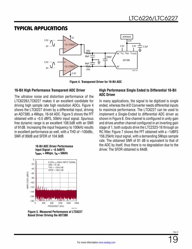
16-Bit High Performance Transparent ADC Driver
The ultralow noise and distortion performance of the LTC6226/LTC6227 makes it an excellent candidate for driving high sample rate high resolution ADCs. Figure 4 shows the LTC6227 driven by a differential input, driving an AD7380, a 4Msps, 16-bit ADC. Figure 5 shows the FFT obtained with a –0.5 dBFS, 50kHz input signal. Spurious free dynamic range is an excellent 108.5dB with an SNR of 91dB. Increasing the input frequency to 100kHz results in excellent performance as well, with a THD of –100dBc, SNR of 89dB and SFDR of 104.9dB.
High Performance Single Ended to Differential 16-Bit ADC Driver
In many applications, the signal to be digitized is single ended, whereas the A/D Converter needs differential inputs to maximize performance. The LTC6227 can be used to implement a Single-Ended to differential ADC driver as shown in Figure 6. One channel is configured in unity gain and drives another channel configured in an inverting gain stage of 1, both outputs drive the LTC2323-16 through an RC filter. Figure 7 shows the FFT obtained with a –1dBFS 156.25kHz input signal, with a demanding 5Msps sample rate. The obtained SNR of 81 dB is equivalent to that of the ADC by itself, thus there is no degradation due to the driver. The SFDR obtained is 84dB.
62267 F04–
+
330pF
3.3V
3.3V
ADR4533
2.5V 2.2µF
1/2 LTC622733Ω
68pF3.3V
0V
68pF
–
+1/2 LTC6227
33Ω
5V
–2.5V
3.3V
0V
AD7380
IN–
IN+ VCC VREF VLOGIC
Figure 4. Transparent Driver for 16-Bit ADC
Figure 5. Measured Performance of LTC6227 Based Driver Driving the AD7380
6.23VP–P 50kHz INPUT SIGNAL
FREQUENCY (kHz)0 400 800 1200 1600 2000
–180
–160
–140
–120
–100
–80
–60
–40
–20
0
AMPL
ITUD
E (d
BFS)
62267 F05
SNR = 91 dBTHD = –104.8 dBSFDR = 108.5 dB
16-Bit ADC Driver PerformanceInput Signal = –0.5dBFSfSMPL = 4Msps, fIN = 50kHz
LTC6226/LTC6227
20Rev 0
For more information www.analog.com
TYPICAL APPLICATIONS
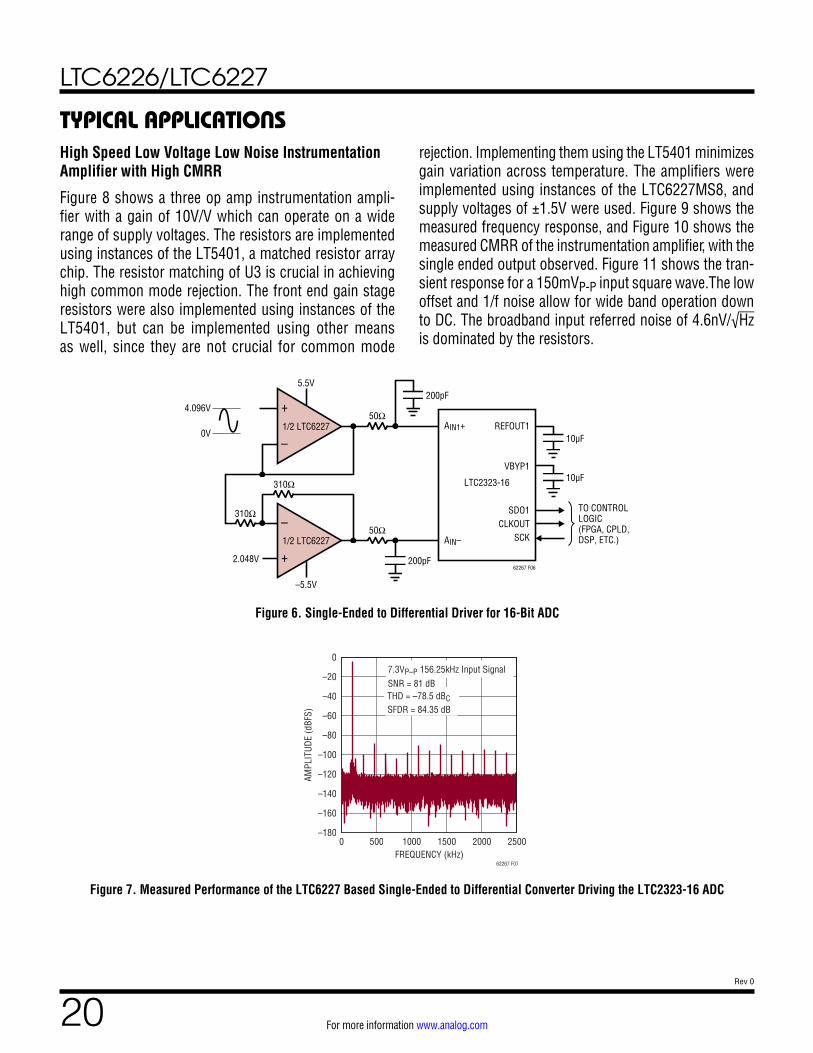
Figure 6. Single-Ended to Differential Driver for 16-Bit ADC
Figure 7. Measured Performance of the LTC6227 Based Single-Ended to Differential Converter Driving the LTC2323-16 ADC
–
+ 200pF62267 F06
TO CONTROLLOGIC(FPGA, CPLD,DSP, ETC.)1/2 LTC6227
AIN1+
AIN–
LTC2323-16
REFOUT1
VBYP1
SDO1CLKOUT
SCK
–
+1/2 LTC6227
50Ω
5.5V
50Ω
310Ω
310Ω
4.096V
0V
–5.5V
2.048V
200pF
10µF
10µF
SNR = 81 dB
SFDR = 84.35 dB
7.3VP–P 156.25kHz Input Signal
THD = –78.5 dBC
FREQUENCY (kHz)0 500 1000 1500 2000 2500
–180
–160
–140
–120
–100
–80
–60
–40
–20
0
AMPL
ITUD
E (d
BFS)
62267 F07
High Speed Low Voltage Low Noise Instrumentation Amplifier with High CMRR
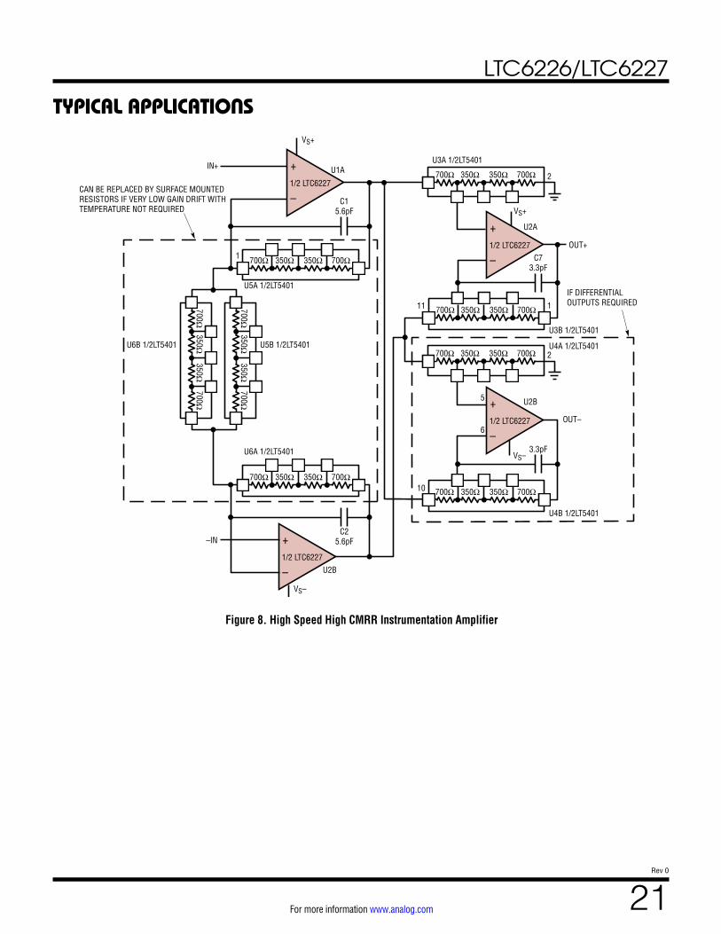
Figure 8 shows a three op amp instrumentation ampli-fier with a gain of 10V/V which can operate on a wide range of supply voltages. The resistors are implemented using instances of the LT5401, a matched resistor array chip. The resistor matching of U3 is crucial in achieving high common mode rejection. The front end gain stage resistors were also implemented using instances of the LT5401, but can be implemented using other means as well, since they are not crucial for common mode
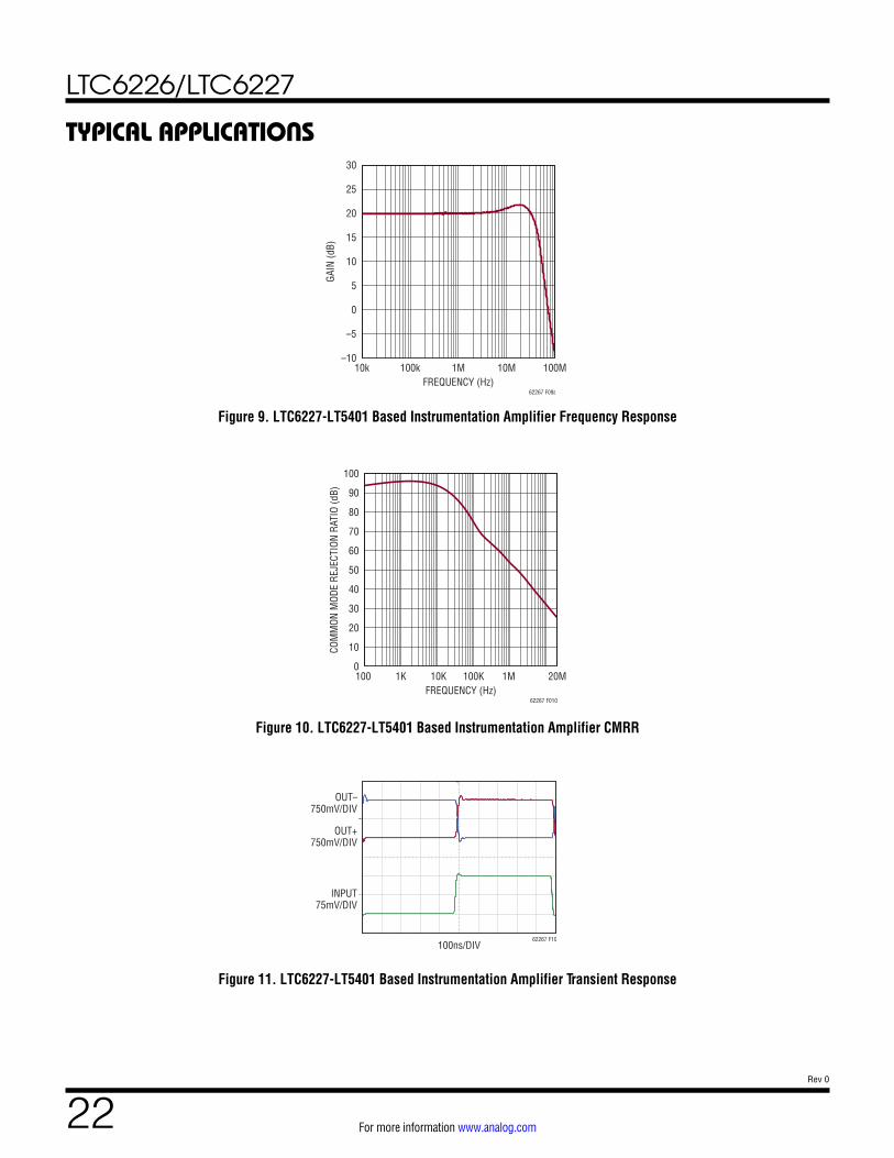
rejection. Implementing them using the LT5401 minimizes gain variation across temperature. The amplifiers were implemented using instances of the LTC6227MS8, and supply voltages of ±1.5V were used. Figure 9 shows the measured frequency response, and Figure 10 shows the measured CMRR of the instrumentation amplifier, with the single ended output observed. Figure 11 shows the tran-sient response for a 150mVP-P input square wave.The low offset and 1/f noise allow for wide band operation down to DC. The broadband input referred noise of 4.6nV/√Hz is dominated by the resistors.
LTC6226/LTC6227
21Rev 0
For more information www.analog.com
TYPICAL APPLICATIONS
Figure 8. High Speed High CMRR Instrumentation Amplifier
–
+
700Ω700Ω 350Ω350Ω
700Ω700Ω 350Ω350Ω
700Ω 2700Ω 350Ω350Ω
700Ω 2
1
700Ω 350Ω350Ω
700Ω700Ω1
U5A 1/2LT5401
U3A 1/2LT5401
U4A 1/2LT5401
IF DIFFERENTIAL OUTPUTS REQUIRED
CAN BE REPLACED BY SURFACE MOUNTEDRESISTORS IF VERY LOW GAIN DRIFT WITH TEMPERATURE NOT REQUIRED
U4B 1/2LT5401
U3B 1/2LT5401
U5B 1/2LT5401U6B 1/2LT5401
350Ω350Ω
700Ω700Ω
U6A 1/2LT5401
C25.6pF
C15.6pF
C73.3pF
3.3pF
U2B
–IN
VS–
350Ω350Ω700Ω
700Ω350Ω
350Ω
700Ω700Ω
350Ω350Ω
1/2 LTC6227
–
+ U1AIN+
VS+
1/2 LTC6227
–
+ U2A
U2B
10
11
5
6
VS+
VS–
OUT–
OUT+1/2 LTC6227
–
+1/2 LTC6227
LTC6226/LTC6227
22Rev 0
For more information www.analog.com
TYPICAL APPLICATIONS
Figure 9. LTC6227-LT5401 Based Instrumentation Amplifier Frequency Response
FREQUENCY (Hz)10k 100k 1M 10M 100M
–10
–5
0
5
10
15
20
25
30
GAIN
(dB)
62267 F09a
FREQUENCY (Hz)100 1K 10K 100K 1M 20M0
10
20
30
40
50
60
70
80
90
100
COM
MON
MOD
E RE
JECT
ION
RATI
O (d
B)
62267 F010
100ns/DIV
OUT+750mV/DIV
OUT–750mV/DIV
INPUT75mV/DIV
62267 F10
Figure 10. LTC6227-LT5401 Based Instrumentation Amplifier CMRR
Figure 11. LTC6227-LT5401 Based Instrumentation Amplifier Transient Response
LTC6226/LTC6227
23Rev 0
For more information www.analog.com
PACKAGE DESCRIPTION
.016 – .050(0.406 – 1.270)
.010 – .020(0.254 – 0.508)
× 45°
0°– 8° TYP.008 – .010
(0.203 – 0.254)
SO8 REV G 0212
.053 – .069(1.346 – 1.752)
.014 – .019(0.355 – 0.483)
TYP
.004 – .010(0.101 – 0.254)
.050(1.270)
BSC
1 2 3 4
.150 – .157(3.810 – 3.988)
NOTE 3
8 7 6 5
.189 – .197(4.801 – 5.004)
NOTE 3
.228 – .244(5.791 – 6.197)
.245MIN .160 ±.005
RECOMMENDED SOLDER PAD LAYOUT
.045 ±.005 .050 BSC
.030 ±.005 TYP
INCHES(MILLIMETERS)
NOTE:1. DIMENSIONS IN
2. DRAWING NOT TO SCALE3. THESE DIMENSIONS DO NOT INCLUDE MOLD FLASH OR PROTRUSIONS. MOLD FLASH OR PROTRUSIONS SHALL NOT EXCEED .006" (0.15mm)4. PIN 1 CAN BE BEVEL EDGE OR A DIMPLE
S8 Package8-Lead Plastic Small Outline (Narrow .150 Inch)
(Reference LTC DWG # 05-08-1610 Rev G)
LTC6226/LTC6227
24Rev 0
For more information www.analog.com
PACKAGE DESCRIPTION
1.50 – 1.75(NOTE 4)
2.80 BSC
0.30 – 0.45 6 PLCS (NOTE 3)
DATUM ‘A’
0.09 – 0.20(NOTE 3) S6 TSOT-23 0302
2.90 BSC(NOTE 4)
0.95 BSC
1.90 BSC
0.80 – 0.90
1.00 MAX0.01 – 0.10
0.20 BSC
0.30 – 0.50 REF
PIN ONE ID
NOTE:1. DIMENSIONS ARE IN MILLIMETERS2. DRAWING NOT TO SCALE3. DIMENSIONS ARE INCLUSIVE OF PLATING4. DIMENSIONS ARE EXCLUSIVE OF MOLD FLASH AND METAL BURR5. MOLD FLASH SHALL NOT EXCEED 0.254mm6. JEDEC PACKAGE REFERENCE IS MO-193
3.85 MAX
0.62MAX
0.95REF
RECOMMENDED SOLDER PAD LAYOUTPER IPC CALCULATOR
1.4 MIN2.62 REF
1.22 REF
S6 Package6-Lead Plastic TSOT-23
(Reference LTC DWG # 05-08-1636)
LTC6226/LTC6227
25Rev 0
For more information www.analog.com
PACKAGE DESCRIPTION
2.00 ±0.10(4 SIDES)
NOTE:1. DRAWING TO BE MADE A JEDEC PACKAGE OUTLINE M0-229 VARIATION OF (WCCD-2)2. DRAWING NOT TO SCALE3. ALL DIMENSIONS ARE IN MILLIMETERS4. DIMENSIONS OF EXPOSED PAD ON BOTTOM OF PACKAGE DO NOT INCLUDE MOLD FLASH. MOLD FLASH, IF PRESENT, SHALL NOT EXCEED 0.15mm ON ANY SIDE5. EXPOSED PAD SHALL BE SOLDER PLATED 6. SHADED AREA IS ONLY A REFERENCE FOR PIN 1 LOCATION ON THE TOP AND BOTTOM OF PACKAGE
0.40 ±0.10
BOTTOM VIEW—EXPOSED PAD
0.60 ±0.10(2 SIDES)
0.75 ±0.05
R = 0.125TYP
R = 0.05TYP
1.37 ±0.10(2 SIDES)
13
64
PIN 1 BARTOP MARK
(SEE NOTE 6)
0.200 REF
0.00 – 0.05
(DC6) DFN REV C 0915
0.25 ±0.050.50 BSC
0.25 ±0.05
1.37 ±0.10(2 SIDES)
RECOMMENDED SOLDER PAD PITCH AND DIMENSIONS
0.60 ±0.10(2 SIDES)
1.15 ±0.05
0.70 ±0.05
2.55 ±0.05
PACKAGEOUTLINE
0.50 BSC
PIN 1 NOTCH R = 0.20 OR 0.25 × 45° CHAMFER
DC6 Package6-Lead Plastic DFN (2mm × 2mm)
(Reference LTC DWG # 05-08-1703 Rev C)
LTC6226/LTC6227
26Rev 0
For more information www.analog.com
PACKAGE DESCRIPTION
MSOP (MS8E) 0213 REV K
0.53 ±0.152(.021 ±.006)
SEATINGPLANE
NOTE:1. DIMENSIONS IN MILLIMETER/(INCH)2. DRAWING NOT TO SCALE3. DIMENSION DOES NOT INCLUDE MOLD FLASH, PROTRUSIONS OR GATE BURRS. MOLD FLASH, PROTRUSIONS OR GATE BURRS SHALL NOT EXCEED 0.152mm (.006") PER SIDE4. DIMENSION DOES NOT INCLUDE INTERLEAD FLASH OR PROTRUSIONS. INTERLEAD FLASH OR PROTRUSIONS SHALL NOT EXCEED 0.152mm (.006") PER SIDE5. LEAD COPLANARITY (BOTTOM OF LEADS AFTER FORMING) SHALL BE 0.102mm (.004") MAX6. EXPOSED PAD DIMENSION DOES INCLUDE MOLD FLASH. MOLD FLASH ON E-PAD SHALL NOT EXCEED 0.254mm (.010") PER SIDE.
0.18(.007)
0.254(.010)
1.10(.043)MAX
0.22 – 0.38(.009 – .015)
TYP
0.86(.034)REF
0.65(.0256)
BSC
0° – 6° TYP
DETAIL “A”
DETAIL “A”
GAUGE PLANE
1 2 3 4
4.90 ±0.152(.193 ±.006)
8
8
1
BOTTOM VIEW OFEXPOSED PAD OPTION
7 6 5
3.00 ±0.102(.118 ±.004)
(NOTE 3)
3.00 ±0.102(.118 ±.004)
(NOTE 4)
0.52(.0205)
REF
1.68(.066)
1.88(.074)
5.10(.201)MIN
3.20 – 3.45(.126 – .136)
1.68 ±0.102(.066 ±.004)
1.88 ±0.102(.074 ±.004) 0.889 ±0.127
(.035 ±.005)
RECOMMENDED SOLDER PAD LAYOUT
0.65(.0256)
BSC0.42 ±0.038
(.0165 ±.0015)TYP
0.1016 ±0.0508(.004 ±.002)
DETAIL “B”
DETAIL “B”CORNER TAIL IS PART OF
THE LEADFRAME FEATURE.FOR REFERENCE ONLY
NO MEASUREMENT PURPOSE
0.05 REF
0.29REF
MS8E Package8-Lead Plastic MSOP, Exposed Die Pad(Reference LTC DWG # 05-08-1662 Rev K)
LTC6226/LTC6227
27Rev 0
For more information www.analog.com
Information furnished by Analog Devices is believed to be accurate and reliable. However, no responsibility is assumed by Analog Devices for its use, nor for any infringements of patents or other rights of third parties that may result from its use. Specifications subject to change without notice. No license is granted by implication or otherwise under any patent or patent rights of Analog Devices.
PACKAGE DESCRIPTION
3.00 ±0.10(4 SIDES)
NOTE:1. DRAWING TO BE MADE A JEDEC PACKAGE OUTLINE M0-229 VARIATION OF (WEED-2). CHECK THE LTC WEBSITE DATA SHEET FOR CURRENT STATUS OF VARIATION ASSIGNMENT2. DRAWING NOT TO SCALE3. ALL DIMENSIONS ARE IN MILLIMETERS4. DIMENSIONS OF EXPOSED PAD ON BOTTOM OF PACKAGE DO NOT INCLUDE MOLD FLASH. MOLD FLASH, IF PRESENT, SHALL NOT EXCEED 0.15mm ON ANY SIDE5. EXPOSED PAD SHALL BE SOLDER PLATED6. SHADED AREA IS ONLY A REFERENCE FOR PIN 1 LOCATION ON THE TOP AND BOTTOM OF PACKAGE
0.40 ±0.10
BOTTOM VIEW—EXPOSED PAD
1.65 ±0.10(2 SIDES)
0.75 ±0.05
R = 0.125TYP
2.38 ±0.10(2 SIDES)
15
106
PIN 1TOP MARK
(SEE NOTE 6)
0.200 REF
0.00 – 0.05
(DD) DFN REV C 0310
0.25 ±0.05
2.38 ±0.05(2 SIDES)
RECOMMENDED SOLDER PAD PITCH AND DIMENSIONS
1.65 ±0.05(2 SIDES)2.15 ±0.05
0.50BSC
0.70 ±0.05
3.55 ±0.05
PACKAGEOUTLINE
0.25 ±0.050.50 BSC
DD Package10-Lead Plastic DFN (3mm × 3mm)
(Reference LTC DWG # 05-08-1699 Rev C)
PIN 1 NOTCHR = 0.20 OR0.35 × 45°CHAMFER
LTC6226/LTC6227
28Rev 0
For more information www.analog.com ANALOG DEVICES, INC. 2020
03/20www.analog.com
RELATED PARTS
TYPICAL APPLICATION
PART NUMBER DESCRIPTION COMMENTS
Operational Amplifiers
LTC6228/LTC6229 Single/Dual High Speed Ultra Low Noise Low Distortion Rail-to-Rail Output Op Amps
0.88 nV/√Hz, 730MHz, 500V/µs Unity Gain Stable
LTC6252/LTC6253/LTC6254
Single/Dual/Quad High Speed Rail-to-Rail Input and Output Op Amps
720MHz, 3.5mA, 2.75nV/√Hz, 280V/µs, 0.35mV, Unity Gain Stable
ADA4899-1 High Speed Ultra Low Noise Ultra Low Distortion 1 nV/√Hz, 600MHz, 310V/µs Unity Gain Stable
LTC6268/LTC6269 Single/Dual High Speed FET Input Op Amp 400MHz, 4nV/√Hz, ±3fA Input Bias Current
LT1818/LT1819 Single/Dual Wide Bandwidth, High Slew Rate Low Noise and Distortion Op Amps
400MHz, 9mA, 6nV/√Hz, 2500V/µs, 1.5mV –85dBc at 5MHz
ADA4896-1/ADA4896-2
Low Noise Low Power Rail-to-Rail Output 3mA 1 nV/√Hz 230 MHz 120 V/µs Unity Gain Stable
LT6230/LT6231/LT6232
Single/Dual/Quad Low Noise Rail-to-Rail Output Op Amps 215MHz, 3.5mA, 1.1nV/√Hz, 70V/µs, 350µV
LTC6246/LTC6247/LTC6248
Single/Dual/Quad High Speed Rail-to-Rail Input and Output Op Amps
180MHz, 1mA, 4.2nV/√Hz, 90V/µs, 0.5mV
LT6200/LT6201 Single/Dual Ultralow Noise Rail-to-Rail Input/Output Op Amps 165MHz, 20mA, 0.95nV/√Hz, 44V/µs, 1mV
LT6202/LT6203/LT6204
Single/Dual/Quad Ultralow Noise Rail-to-Rail Op Amp 100MHz, 3mA, 1.9nV/√Hz, 25V/µs, 0.5mV
LT1801/LT1802 Dual/Quad Low Power High Speed Rail-to-Rail Input and Output Op Amps
80MHz, 2mA, 8.5nV√Hz, 25V/µs, 350µV
LT1028 Ultralow Noise, Precision High Speed Op Amps 75MHz, 9.5mA, 0.85nV/√Hz, 11V/µs, 40µV
LTC6350 Low Noise Single-Ended to Differential Converter/ADC Driver 33MHz (–3dB), 4.8mA, 1.9nV/√Hz, 240ns Settling to 0.01% 8VP-P
ADCs
LTC2387-18 18-Bit, 15Msps SAR-ADC 95.7dB SNR
AD7380 4Msps 16-Bit SAR-ADC 92dB DNR SNR, 6.6 VP-P Input Range
LTC2323-16 5Msps 16-Bit SAR-ADC 81dB SNR,8VP-P Input Range
AD4020 1.8 Msps 20-Bit SAR-ADC 99 dB SNR
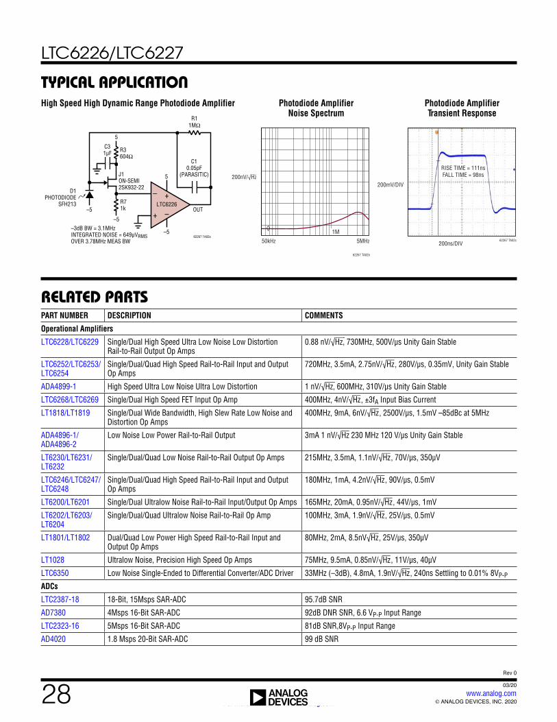
High Speed High Dynamic Range Photodiode Amplifier Photodiode Amplifier Noise Spectrum
Photodiode Amplifier Transient Response
62267 TA02a
R11MΩ
D1PHOTODIODE
SFH213 R71k
–3dB BW = 3.1MHzINTEGRATED NOISE = 649µVRMSOVER 3.78MHz MEAS BW
C31µF R3
604Ω
J1ON-SEMI2SK932-22
–5
–5
–5
5
5
OUT
–
–+
+
C10.05pF
(PARASITIC)
LTC6226
50kHz 5MHz
200nV/√Hz
62267 TA02b
1M
200ns/DIV
200mV/DIV
RISE TIME = 111nsFALL TIME = 98ns
62267 TA02c