![Large effects of subtle electronic correlations on the ... · e ect of the cancellation of errors in the exchange and correlation parts of the density functional [5]. As has been](https://static.fdocument.org/doc/165x107/5f26cf038440797307756f66/large-effects-of-subtle-electronic-correlations-on-the-e-ect-of-the-cancellation.jpg)
Latched Comparator - EECS Instructional Support …ee247/fa05/lectures/L21_f05.pdfComparator Example...
28
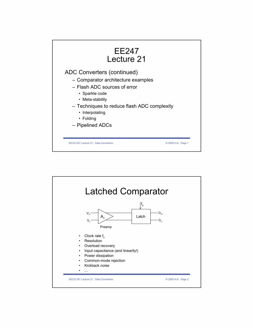
EECS 247 Lecture 21: Data Converters © 2005 H.K. Page 1 EE247 Lecture 21 ADC Converters (continued) – Comparator architecture examples – Flash ADC sources of error • Sparkle code • Meta-stability – Techniques to reduce flash ADC complexity • Interpolating • Folding – Pipelined ADCs EECS 247 Lecture 21: Data Converters © 2005 H.K. Page 2 Latched Comparator • Clock rate f s • Resolution • Overload recovery • Input capacitance (and linearity!) • Power dissipation • Common-mode rejection • Kickback noise • … A v Latch V i+ V i- D o+ D o- f s Preamp
Transcript of Latched Comparator - EECS Instructional Support …ee247/fa05/lectures/L21_f05.pdfComparator Example...
EECS 247 Lecture 21: Data Converters © 2005 H.K. Page 1
EE247Lecture 21
ADC Converters (continued)– Comparator architecture examples– Flash ADC sources of error
• Sparkle code• Meta-stability
– Techniques to reduce flash ADC complexity• Interpolating• Folding
– Pipelined ADCs
EECS 247 Lecture 21: Data Converters © 2005 H.K. Page 2
Latched Comparator
• Clock rate fs• Resolution• Overload recovery• Input capacitance (and linearity!)• Power dissipation• Common-mode rejection• Kickback noise• …
Av LatchVi+
Vi-
Do+
Do-
fs
Preamp
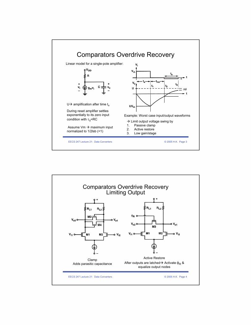
EECS 247 Lecture 21: Data Converters © 2005 H.K. Page 3
Comparators Overdrive Recovery
U amplification after time ta
During reset amplifier settles exponentially to its zero input condition with τ0=RC
Assume Vm maximum input normalized to 1/2lsb (=1)
Linear model for a single-pole amplifier:
Example: Worst case input/output waveforms
Limit output voltage swing by1. Passive clamp2. Active restore3. Low gain/stage
EECS 247 Lecture 21: Data Converters © 2005 H.K. Page 4
Comparators Overdrive RecoveryLimiting Output
ClampAdds parasitic capacitance
Active RestoreAfter outputs are latched Activate φR &
equalize output nodes
EECS 247 Lecture 21: Data Converters © 2005 H.K. Page 5
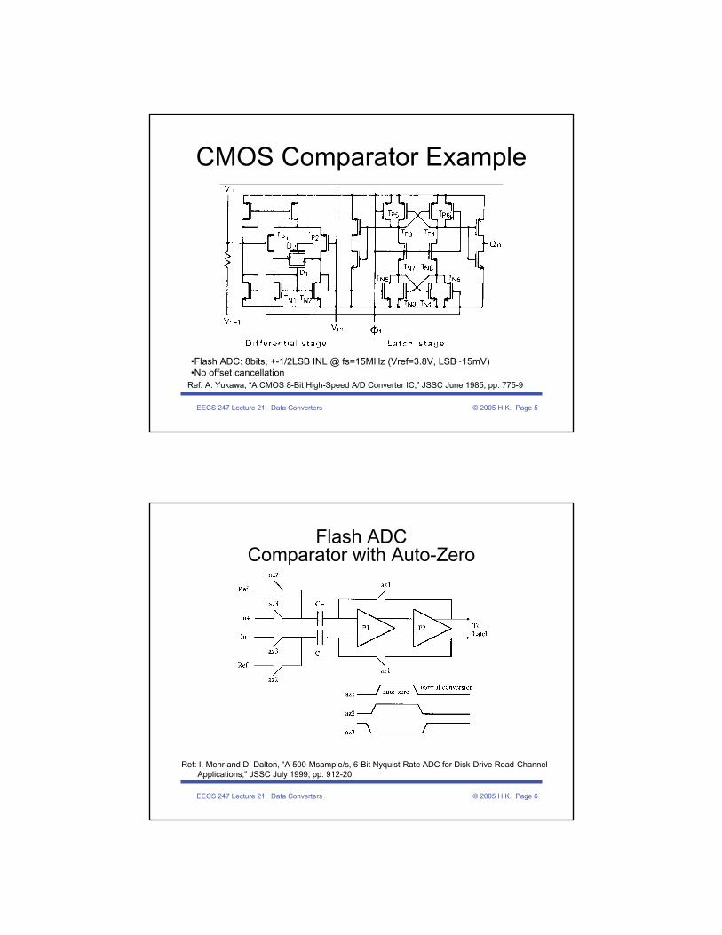
CMOS Comparator Example
Ref: A. Yukawa, “A CMOS 8-Bit High-Speed A/D Converter IC,” JSSC June 1985, pp. 775-9
•Flash ADC: 8bits, +-1/2LSB INL @ fs=15MHz (Vref=3.8V, LSB~15mV)•No offset cancellation
EECS 247 Lecture 21: Data Converters © 2005 H.K. Page 6
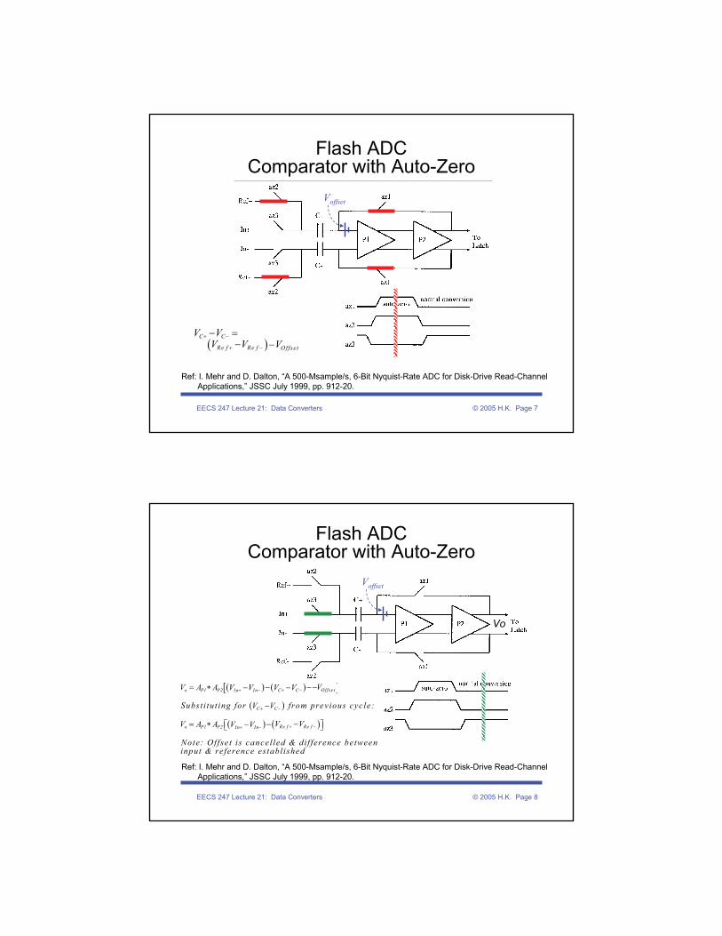
Flash ADCComparator with Auto-Zero
Ref: I. Mehr and D. Dalton, “A 500-Msample/s, 6-Bit Nyquist-Rate ADC for Disk-Drive Read-Channel Applications,” JSSC July 1999, pp. 912-20.
EECS 247 Lecture 21: Data Converters © 2005 H.K. Page 7
Ref: I. Mehr and D. Dalton, “A 500-Msample/s, 6-Bit Nyquist-Rate ADC for Disk-Drive Read-Channel Applications,” JSSC July 1999, pp. 912-20.
Voffset
( )C C
Re f Re f Offset
V VV V V
+ −
+ −
− =− −
Flash ADCComparator with Auto-Zero
EECS 247 Lecture 21: Data Converters © 2005 H.K. Page 8
Ref: I. Mehr and D. Dalton, “A 500-Msample/s, 6-Bit Nyquist-Rate ADC for Disk-Drive Read-Channel Applications,” JSSC July 1999, pp. 912-20.
Voffset
Vo
( ) ( )[ ]( )
( ) ( )
Offseto P1 P2 In In C C
C C
Re f Re fo P1 P2 In In
VV A A V V V V
Substi tut ing for from prev ious cyc le:V V
V VV A A V V
Note: Offse t is cancelled & dif ference be tweeninput & re ference established
+ − + −
+ −
+ −+ −
− −−= ∗ − −
−
−= ∗ −⎡ − ⎤⎣ ⎦
Flash ADCComparator with Auto-Zero
EECS 247 Lecture 21: Data Converters © 2005 H.K. Page 9
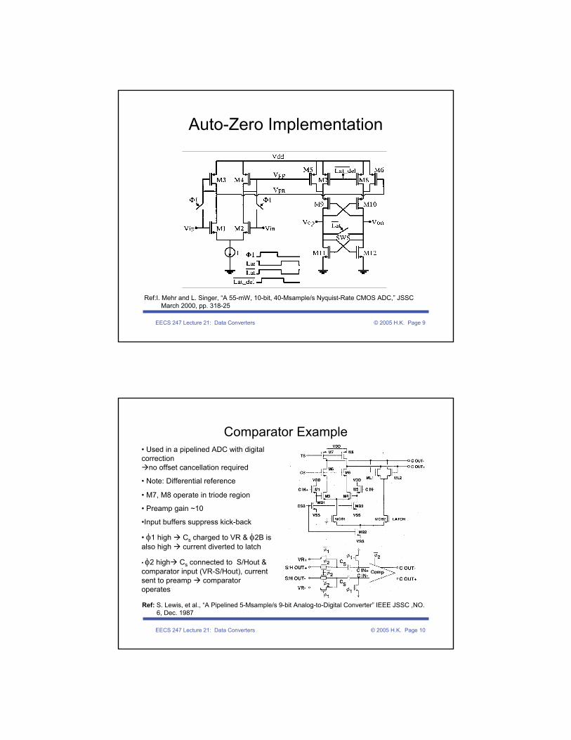
Auto-Zero Implementation
Ref:I. Mehr and L. Singer, “A 55-mW, 10-bit, 40-Msample/s Nyquist-Rate CMOS ADC,” JSSC March 2000, pp. 318-25
EECS 247 Lecture 21: Data Converters © 2005 H.K. Page 10
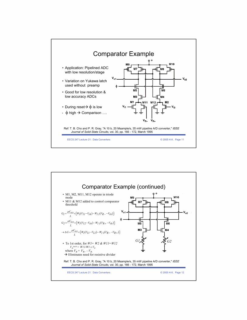
Comparator Example• Used in a pipelined ADC with digital correction
no offset cancellation required
• Note: Differential reference
• M7, M8 operate in triode region
• Preamp gain ~10
•Input buffers suppress kick-back
• φ1 high Cs charged to VR & φ2B is also high current diverted to latch
• φ2 high Cs connected to S/Hout & comparator input (VR-S/Hout), current sent to preamp comparator operates
Ref: S. Lewis, et al., “A Pipelined 5-Msample/s 9-bit Analog-to-Digital Converter” IEEE JSSC ,NO. 6, Dec. 1987
EECS 247 Lecture 21: Data Converters © 2005 H.K. Page 11
Comparator Example
Ref: T. B. Cho and P. R. Gray, "A 10 b, 20 Msample/s, 35 mW pipeline A/D converter," IEEE Journal of Solid-State Circuits, vol. 30, pp. 166 - 172, March 1995
• Application: Pipelined ADC with low resolution/stage
• Variation on Yukawa latch used without preamp
• Good for low resolution & low accuracy ADCs
• During reset φ is low• φ high Comparison ….
Vo1
EECS 247 Lecture 21: Data Converters © 2005 H.K. Page 12
Comparator Example (continued)
Ref: T. B. Cho and P. R. Gray, "A 10 b, 20 Msample/s, 35 mW pipeline A/D converter," IEEE Journal of Solid-State Circuits, vol. 30, pp. 166 - 172, March 1995
Vo1
G1 G2
( ) ( )
( ) ( )
( ) ( )
Cox V V V VG W WI1 th R th1 1 11L
Cox V V V VG W WI2 th R th2 1 11L
Cox V V V VG W WI1 I2 R R1 11L
μ
μ
μ
− −= × −⎡ ⎤−⎣ ⎦
− −= × −⎡ ⎤+⎣ ⎦
− −→Δ = × −⎡ ⎤− +⎣ ⎦
Vo1 Vo2
• M1, M2, M11, M12 operate in triode mode
• M11 & M12 added to control comparator threshold
• To 1st order, for W1= W2 & W11=W12Vth
latch = W11/W1 x VR
where VR = VR+ - VR-Eliminates need for resistive divider
EECS 247 Lecture 21: Data Converters © 2005 H.K. Page 13
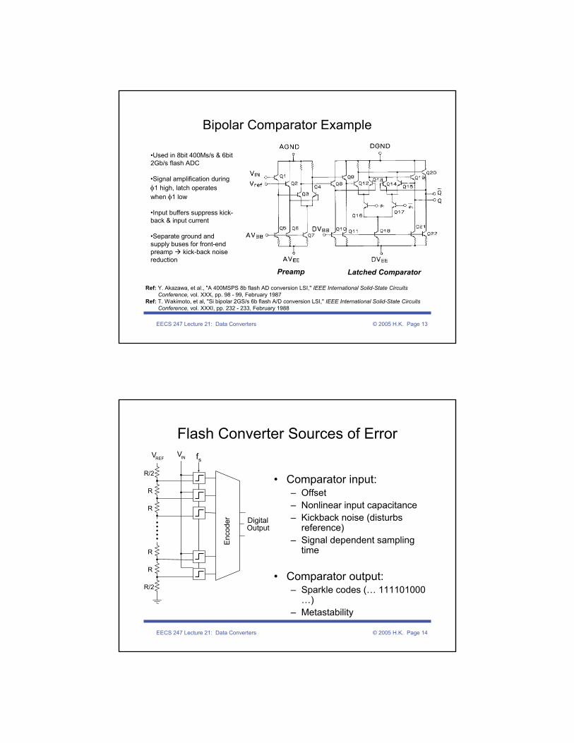
Bipolar Comparator Example
•Used in 8bit 400Ms/s & 6bit 2Gb/s flash ADC
•Signal amplification during φ1 high, latch operates when φ1 low
•Input buffers suppress kick-back & input current
•Separate ground and supply buses for front-end preamp kick-back noise reduction
Ref: Y. Akazawa, et al., "A 400MSPS 8b flash AD conversion LSI," IEEE International Solid-State Circuits Conference, vol. XXX, pp. 98 - 99, February 1987
Ref: T. Wakimoto, et al, "Si bipolar 2GS/s 6b flash A/D conversion LSI," IEEE International Solid-State Circuits Conference, vol. XXXI, pp. 232 - 233, February 1988
Preamp Latched Comparator
EECS 247 Lecture 21: Data Converters © 2005 H.K. Page 14
Flash Converter Sources of Error
• Comparator input:– Offset– Nonlinear input capacitance– Kickback noise (disturbs
reference)– Signal dependent sampling
time
• Comparator output:– Sparkle codes (… 111101000
…)– Metastability
R/2
R
R
R
R/2
R
Enc
oder Digital
Output
VINVREF fs
.....
EECS 247 Lecture 21: Data Converters © 2005 H.K. Page 15
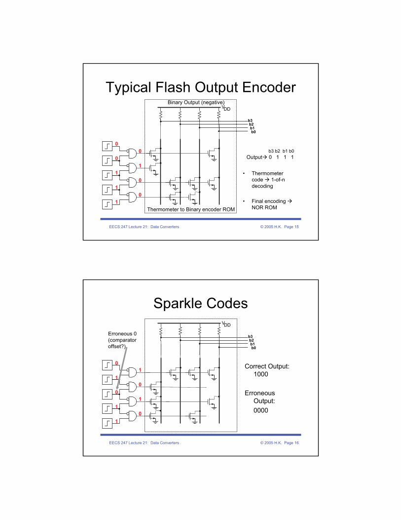
Typical Flash Output Encoder
0
0
1
1
1
0
1
0
0
Binary Output (negative)
Thermometer to Binary encoder ROM
VDD
• Thermometer code 1-of-n decoding
• Final encoding NOR ROM
b3b2b1b0
b3 b2 b1 b0Output 0 1 1 1
EECS 247 Lecture 21: Data Converters © 2005 H.K. Page 16
Sparkle Codes
Correct Output:1000
Erroneous Output:0000
0
1
0
1
1
1
0
1
0
Erroneous 0 (comparator offset?)
VDD
b3b2b1b0
EECS 247 Lecture 21: Data Converters © 2005 H.K. Page 17
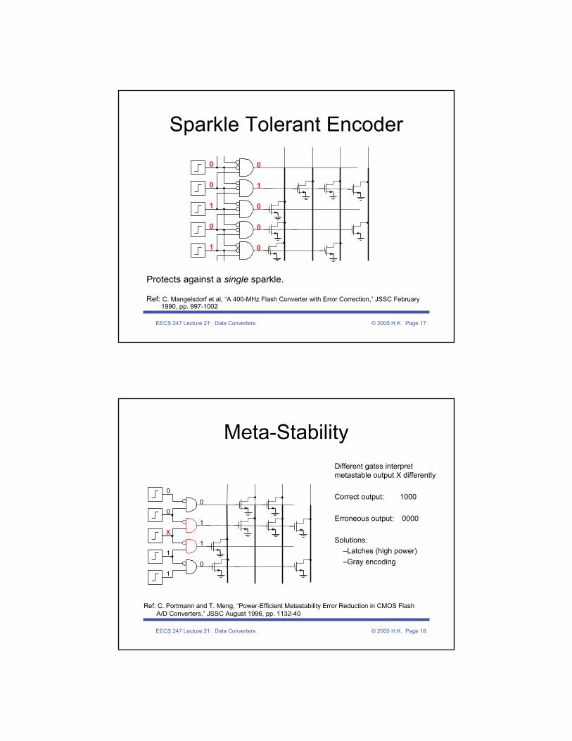
Sparkle Tolerant Encoder
Protects against a single sparkle.
Ref: C. Mangelsdorf et al, “A 400-MHz Flash Converter with Error Correction,” JSSC February 1990, pp. 997-1002
0
0
1
0
1
0
1
0
0
0
EECS 247 Lecture 21: Data Converters © 2005 H.K. Page 18
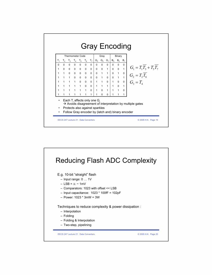
Meta-StabilityDifferent gates interpret metastable output X differently
Correct output: 1000
Erroneous output: 0000
Solutions:–Latches (high power)–Gray encoding
Ref: C. Portmann and T. Meng, “Power-Efficient Metastability Error Reduction in CMOS Flash A/D Converters,” JSSC August 1996, pp. 1132-40
0
0
X
1
1
0
1
1
0
EECS 247 Lecture 21: Data Converters © 2005 H.K. Page 19
Gray Encoding
• Each Ti affects only one GiAvoids disagreement of interpretation by multiple gates
• Protects also against sparkles• Follow Gray encoder by (latch and) binary encoder
BinaryGrayThermometer Code
1110011111111
0111010111111
1011110011111
0010110001111
1100100000111
0101100000011
1001000000001
0000000000000
B1B2B3G1G2G3T7T6T5T4T3T2T1
43
622
75311
TGTTG
TTTTG
==
+=
EECS 247 Lecture 21: Data Converters © 2005 H.K. Page 20
Reducing Flash ADC Complexity
E.g. 10-bit “straight” flash– Input range: 0 … 1V– LSB = Δ: ~ 1mV – Comparators: 1023 with offset << LSB– Input capacitance: 1023 * 100fF = 102pF– Power: 1023 * 3mW = 3W
Techniques to reduce complexity & power dissipation :– Interpolation– Folding– Folding & Interpolation– Two-step, pipelining
EECS 247 Lecture 21: Data Converters © 2005 H.K. Page 21
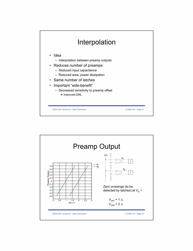
Interpolation
• Idea– Interpolation between preamp outputs
• Reduces number of preamps– Reduced input capacitance– Reduced area, power dissipation
• Same number of latches• Important “side-benefit”
– Decreased sensitivity to preamp offsetimproved DNL
EECS 247 Lecture 21: Data Converters © 2005 H.K. Page 22
Preamp Output
Zero crossings (to be detected by latches) at Vin =
Vref1 = 1 ΔVref2 = 2 Δ
0 0.5 1 1.5 2 2.5 3
-0.5-0.4-0.3-0.2-0.1
00.10.20.30.40.5
Vin / Δ
Pre
amp
Out
put
A1A2
VinA1
A2
EECS 247 Lecture 21: Data Converters © 2005 H.K. Page 23
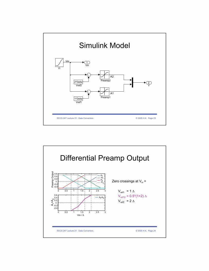
Simulink Model
2Y
1Vin
2*DeltaVref2
1*DeltaVref1
Vi
Preamp2
Preamp1
Vin
A2
A1
EECS 247 Lecture 21: Data Converters © 2005 H.K. Page 24
Differential Preamp Output
Zero crossings at Vin =
Vref1 = 1 ΔVref12 = 0.5*(1+2) ΔVref2 = 2 Δ
0 0.5 1 1.5 2 2.5 3
-0.4-0.2
00.20.40.6
Pre
amp
Out
put
0 0.5 1 1.5 2 2.5 3
-0.4-0.2
00.20.40.6
A 1+A
2
A1-A1A2-A2
A1+A2
Vin / Δ
EECS 247 Lecture 21: Data Converters © 2005 H.K. Page 25
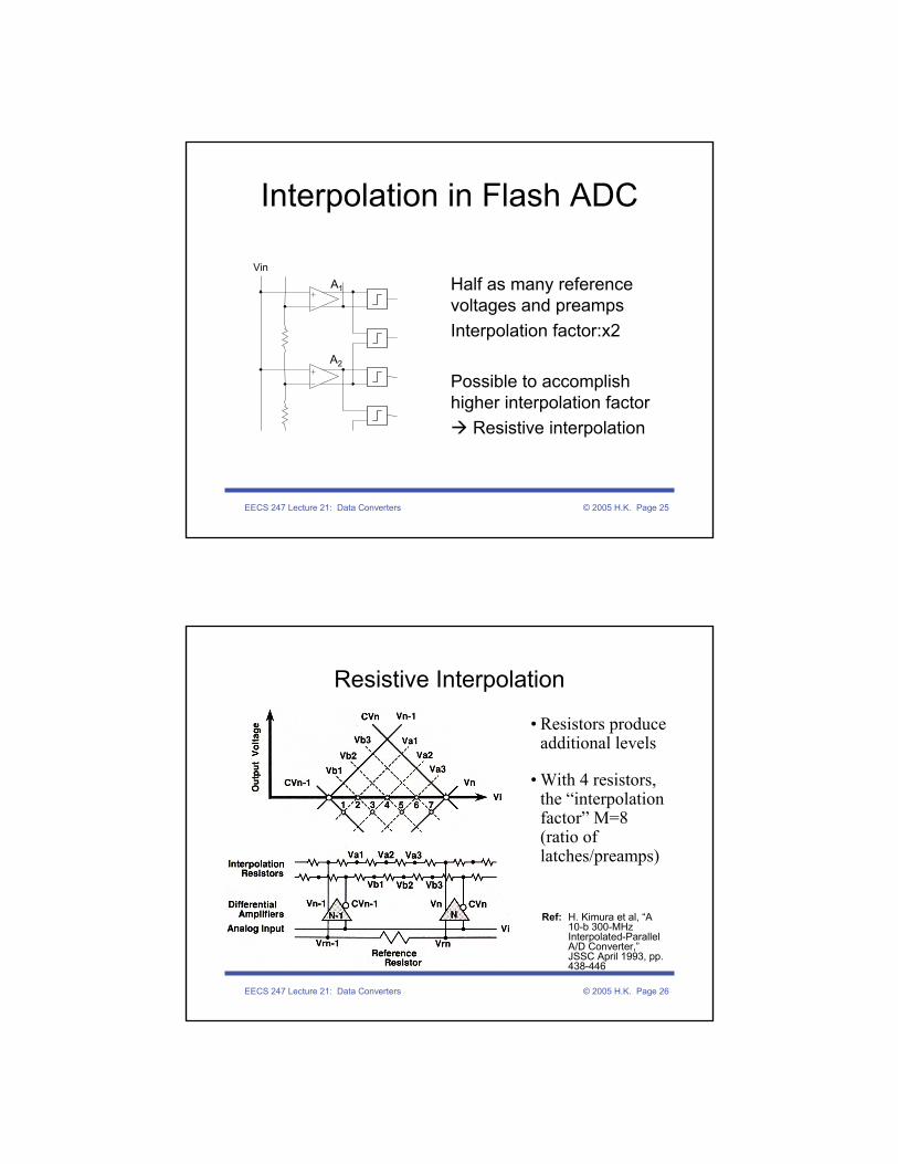
Interpolation in Flash ADC
Half as many reference voltages and preamps Interpolation factor:x2
Possible to accomplish higher interpolation factor
Resistive interpolation
Vin
A1
A2
EECS 247 Lecture 21: Data Converters © 2005 H.K. Page 26
Resistive Interpolation
Ref: H. Kimura et al, “A 10-b 300-MHz Interpolated-Parallel A/D Converter,” JSSC April 1993, pp. 438-446
• Resistors produce additional levels
• With 4 resistors, the “interpolation factor” M=8(ratio of latches/preamps)
EECS 247 Lecture 21: Data Converters © 2005 H.K. Page 27
DNL Improvement• Preamp offset distributed over
M resistively interpolated voltages:
impact on DNL divided by M
• Latch offset divided by gain of preamp
use “large” preamp gain …
Ref: H. Kimura et al, “A 10-b 300-MHz Interpolated-Parallel A/D Converter,” JSSC April 1993, pp. 438-446
EECS 247 Lecture 21: Data Converters © 2005 H.K. Page 28
Preamp Input Range
Linear preamp input ranges must overlapi.e. range > Δ
Sets upper bound on preamp gain << VDD / Δ
0 0.5 1 1.5 2 2.5 3
-0.4-0.2
00.20.40.6
A1-A1A2-A2
0 0.5 1 1.5 2 2.5 3
-0.4-0.2
00.20.40.6
A1+A2
Pre
amp
Out
put
A 1+A
2
Vin / Δ
EECS 247 Lecture 21: Data Converters © 2005 H.K. Page 29
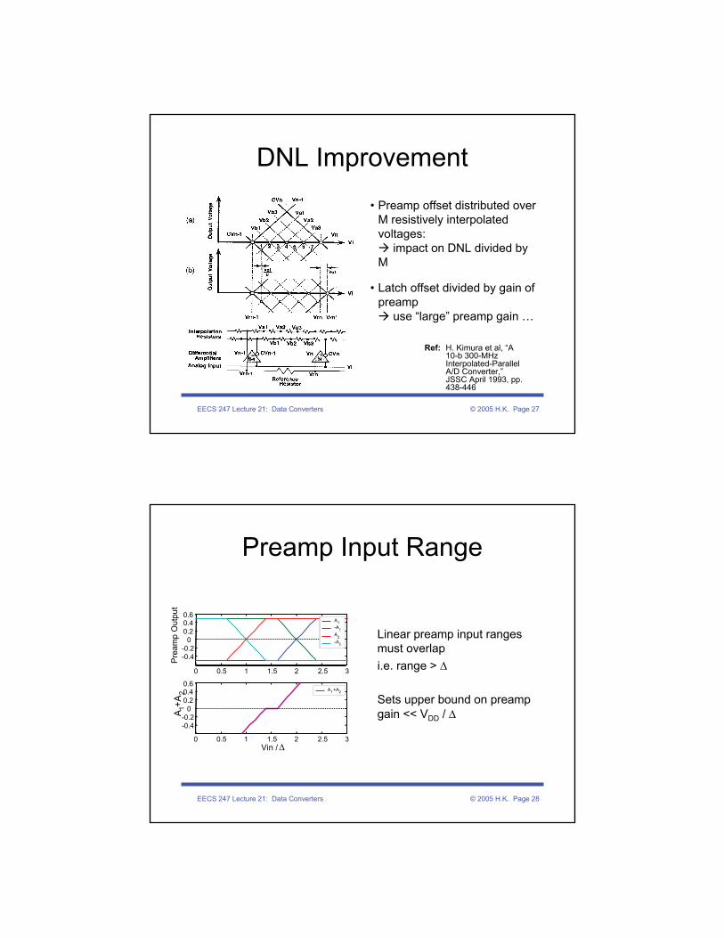
Interpolated-Parallel ADC
Ref: H. Kimura et al, “A 10-b 300-MHz Interpolated-Parallel A/D Converter,” JSSC April 1993, pp. 438-446
10-bit overall resolution:7-bit flash (127
comparators and 128 resistors) & x8 interpolation
EECS 247 Lecture 21: Data Converters © 2005 H.K. Page 30
Measured Performance
Ref: H. Kimura et al, “A 10-b 300-MHz Interpolated-Parallel A/D Converter,” JSSC April 1993, pp. 438-446
(7+3)
Low inputcapacitance
EECS 247 Lecture 21: Data Converters © 2005 H.K. Page 31
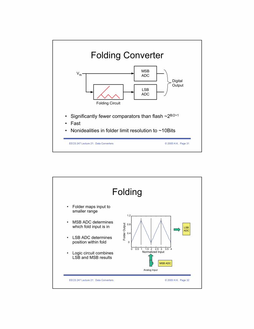
Folding Converter
• Significantly fewer comparators than flash ~2B/2+1
• Fast• Nonidealities in folder limit resolution to ~10Bits
LSBADC
MSBADC
Folding Circuit
VIN
DigitalOutput
EECS 247 Lecture 21: Data Converters © 2005 H.K. Page 32
Folding• Folder maps input to
smaller range
• MSB ADC determines which fold input is in
• LSB ADC determines position within fold
• Logic circuit combines LSB and MSB results
MSB ADC
LSBADC
Analog Input
0 0.5 1 1.5 2 2.5 3 3.5 4
0
0.4
0.8
1.2
Fold
er O
utpu
t
Normalized Input
EECS 247 Lecture 21: Data Converters © 2005 H.K. Page 33
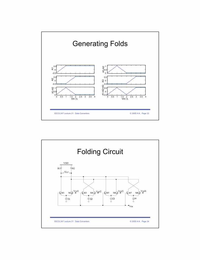
Generating Folds
-0.5
0
0.5
A1
-0.5
0
0.5
A2
0 0.5 1 1.5 2 2.5 3 3.5 40
0.5
1
A1-
A2
0
0.5
1
A1-
A2
-0.5
0
0.5
A3
0 0.5 1 1.5 2 2.5 3 3.5 4-0.5
0
0.5
A1-
A2+
A3
Vin /ΔVin /Δ
EECS 247 Lecture 21: Data Converters © 2005 H.K. Page 34
Folding Circuit
M1 M2
I1
Vref1M3 M4
I2
Vref2 M5 M6
I3
Vref3M7 M8
I4
Vref4
R1 R2
VDD
-Vo+
Vin
EECS 247 Lecture 21: Data Converters © 2005 H.K. Page 35
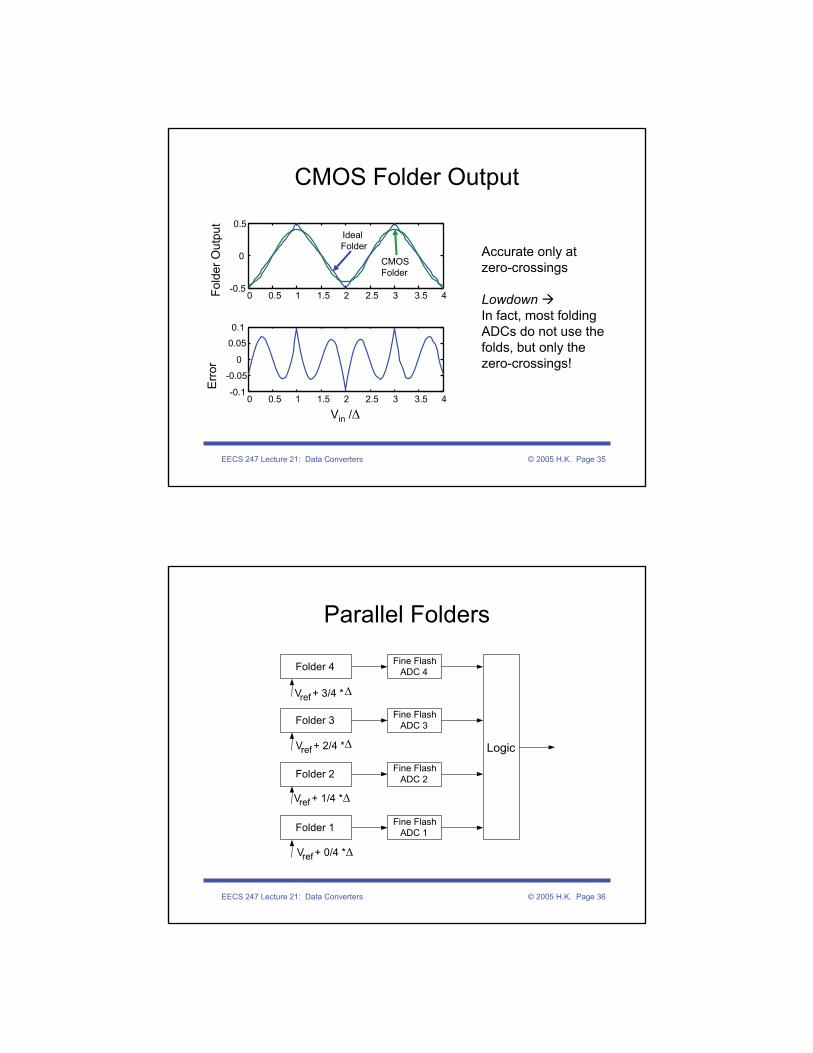
CMOS Folder Output
Accurate only at zero-crossings
LowdownIn fact, most folding ADCs do not use the folds, but only the zero-crossings!
0 0.5 1 1.5 2 2.5 3 3.5 4-0.5
0
0.5Fo
lder
Out
put
0 0.5 1 1.5 2 2.5 3 3.5 4-0.1
-0.05
0
0.05
0.1
Erro
r
Vin /Δ
Ideal Folder
CMOS Folder
EECS 247 Lecture 21: Data Converters © 2005 H.K. Page 36
Parallel Folders
Vref + 3/4 * Δ
Fine FlashADC 4
Folder 3 Fine FlashADC 3
Folder 2 Fine FlashADC 2
Folder 1 Fine FlashADC 1
Folder 4
LogicVref + 2/4 * Δ
Vref + 1/4 * Δ
Vref + 0/4 * Δ
EECS 247 Lecture 21: Data Converters © 2005 H.K. Page 37
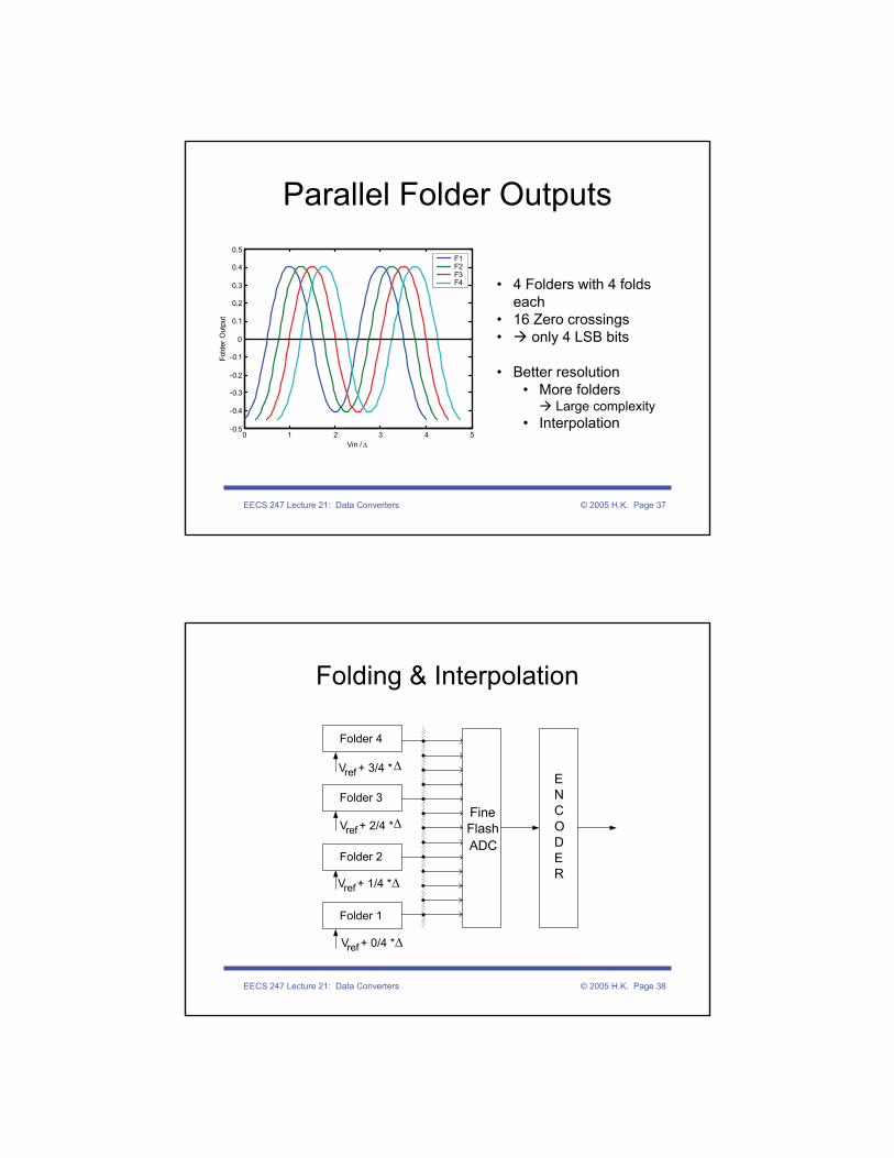
Parallel Folder Outputs
0 1 2 3 4 5-0.5
-0.4
-0.3
-0.2
-0.1
0
0.1
0.2
0.3
0.4
0.5
Vin / Δ
Fold
er O
utpu
t
F1F2F3F4 • 4 Folders with 4 folds
each• 16 Zero crossings• only 4 LSB bits
• Better resolution• More folders
Large complexity• Interpolation
EECS 247 Lecture 21: Data Converters © 2005 H.K. Page 38
Folding & Interpolation
FineFlashADC
ENCODER
Vref + 3/4 * Δ
Folder 3
Folder 2
Folder 1
Folder 4
Vref + 2/4 * Δ
Vref + 1/4 * Δ
Vref + 0/4 * Δ
EECS 247 Lecture 21: Data Converters © 2005 H.K. Page 39
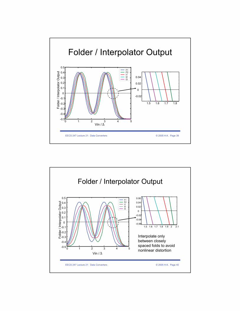
Folder / Interpolator Output
0 1 2 3 5-0.5
-0.4
-0.3
-0.2
-0.1
0
0.1
0.2
0.3
0.4
0.5
Vin / Δ
Fold
er /
Inte
rpol
ator
Out
put F1
F2I1I2I3
1.5 1.6 1.7 1.8
-0.02
0
0.02
0.04
4
EECS 247 Lecture 21: Data Converters © 2005 H.K. Page 40
Folder / Interpolator Output
Interpolate only between closely spaced folds to avoid nonlinear distortion
1.5 1.6 1.7 1.8 1.9 2 2.1-0.06
-0.04
-0.02
0
0.02
0.04
0.06
0 1 2 3 4 5-0.5
-0.4
-0.3
-0.2
-0.1
0
0.1
0.2
0.3
0.4
0.5
Fold
er /
Inte
rpol
ator
Out
put F1
F2I1I2I3
Vin / Δ
EECS 247 Lecture 21: Data Converters © 2005 H.K. Page 41
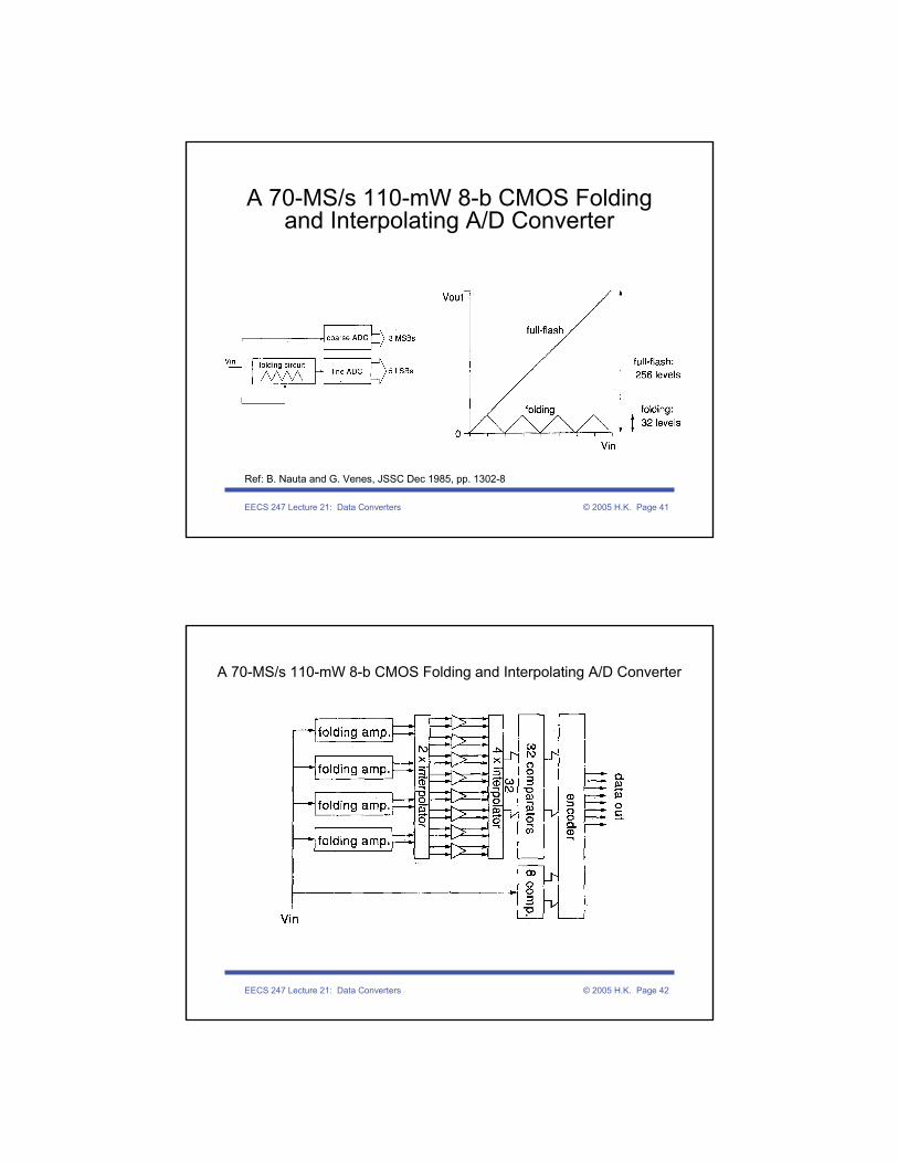
A 70-MS/s 110-mW 8-b CMOS Folding and Interpolating A/D Converter
Ref: B. Nauta and G. Venes, JSSC Dec 1985, pp. 1302-8
EECS 247 Lecture 21: Data Converters © 2005 H.K. Page 42
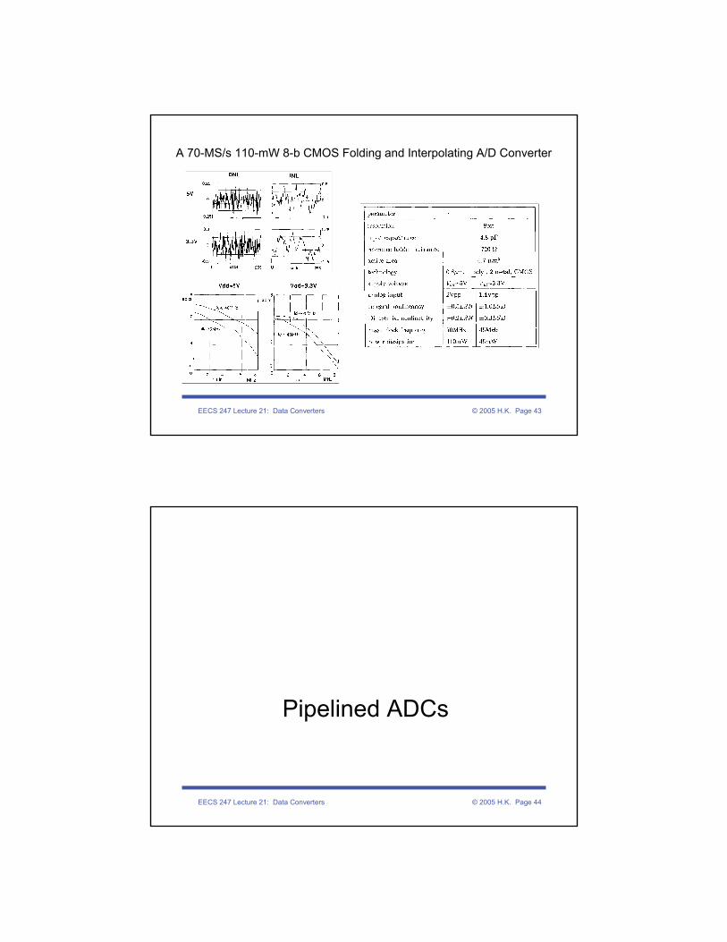
A 70-MS/s 110-mW 8-b CMOS Folding and Interpolating A/D Converter
EECS 247 Lecture 21: Data Converters © 2005 H.K. Page 43
A 70-MS/s 110-mW 8-b CMOS Folding and Interpolating A/D Converter
EECS 247 Lecture 21: Data Converters © 2005 H.K. Page 44
Pipelined ADCs
EECS 247 Lecture 21: Data Converters © 2005 H.K. Page 45
Pipelined A/D Converters
• Ideal operation• Errors and correction
– Redundancy– Digital calibration
• Implementation – Practical circuits– Stage scaling
EECS 247 Lecture 21: Data Converters © 2005 H.K. Page 46
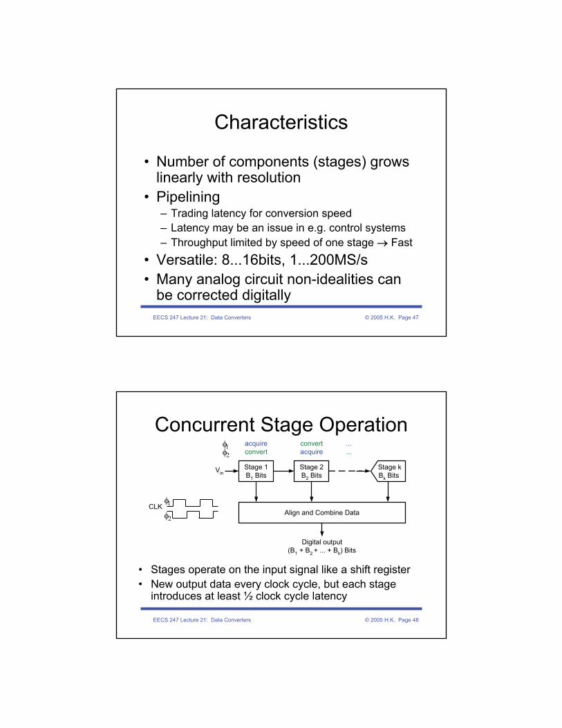
Block Diagram
• Idea: Cascade several low resolution stages to obtain high overall resolution
• Each stage performs coarse A/D conversion and computes its quantization error, or "residue"
Align and Combine Data
Stage 1B1 Bits
Stage 2B2 Bits
Digital output(B1 + B2 + ... + Bk) Bits
Vin
MSB... ...LSB
Stage k Bk Bits
Vres1 Vres2
EECS 247 Lecture 21: Data Converters © 2005 H.K. Page 47
Characteristics
• Number of components (stages) grows linearly with resolution
• Pipelining– Trading latency for conversion speed– Latency may be an issue in e.g. control systems– Throughput limited by speed of one stage → Fast
• Versatile: 8...16bits, 1...200MS/s• Many analog circuit non-idealities can
be corrected digitally
EECS 247 Lecture 21: Data Converters © 2005 H.K. Page 48
Concurrent Stage Operation
• Stages operate on the input signal like a shift register• New output data every clock cycle, but each stage
introduces at least ½ clock cycle latency
Align and Combine Data
Stage 1B1 Bits
Stage 2B2 Bits
Digital output(B1 + B2 + ... + Bk) Bits
VinStage kBk Bits
φ1φ2
acquireconvert
convertacquire
...
...
CLKφ1φ2
EECS 247 Lecture 21: Data Converters © 2005 H.K. Page 49
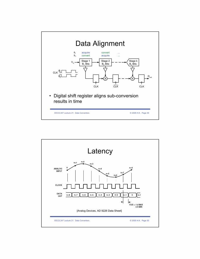
Data Alignment
• Digital shift register aligns sub-conversion results in time
Stage 2B2 Bits
VinStage kBk Bits
φ1φ2
acquireconvert
convertacquire
...
...
+ +Dout
CLK CLK CLK
Stage 1B1 Bits
CLKφ1φ2
EECS 247 Lecture 21: Data Converters © 2005 H.K. Page 50
Latency
[Analog Devices, AD 9226 Data Sheet]
EECS 247 Lecture 21: Data Converters © 2005 H.K. Page 51
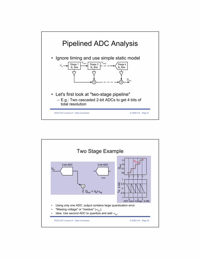
Pipelined ADC Analysis
• Ignore timing and use simple static model
• Let's first look at "two-stage pipeline"– E.g.: Two cascaded 2-bit ADCs to get 4 bits of
total resolution
Stage 2B2 Bits
Vin Stage k Bk Bits
+Dout
Stage 1B1 Bits
+
Vres1 Vres2
EECS 247 Lecture 21: Data Converters © 2005 H.K. Page 52
Two Stage Example
• Using only one ADC: output contains large quantization error• "Missing voltage" or "residue" (-εq1)• Idea: Use second ADC to quantize and add -εq1
0 1 2 300
01
10
11
0 1 2 3-1
-0.5
0
0.5
1
[LS
B]
ADC Input Voltage [LSB]
Vin
+Dout = Vin + εq1
2-bit ADC 2-bit ADC
???
ε q1
D out
Vin
EECS 247 Lecture 21: Data Converters © 2005 H.K. Page 53
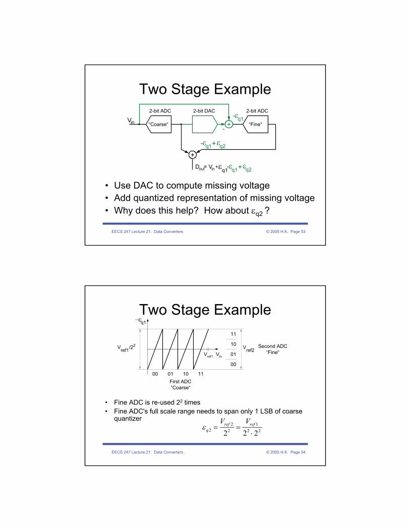
Two Stage Example
• Use DAC to compute missing voltage• Add quantized representation of missing voltage• Why does this help? How about εq2 ?
Vin “Coarse“
+
Dout= Vin + εq1
2-bit ADC 2-bit ADC
“Fine“+-
2-bit DAC-εq1
-εq1+εq2
-εq1+εq2
EECS 247 Lecture 21: Data Converters © 2005 H.K. Page 54
Two Stage Example
• Fine ADC is re-used 22 times• Fine ADC's full scale range needs to span only 1 LSB of coarse
quantizer
221
22
2 222 ⋅== refref
q
VVε
00 01 10 11
Vref1/22
−εq1
00
01
10
11
First ADC“Coarse“
Second ADC“Fine“VinVref1
Vref2
EECS 247 Lecture 21: Data Converters © 2005 H.K. Page 55
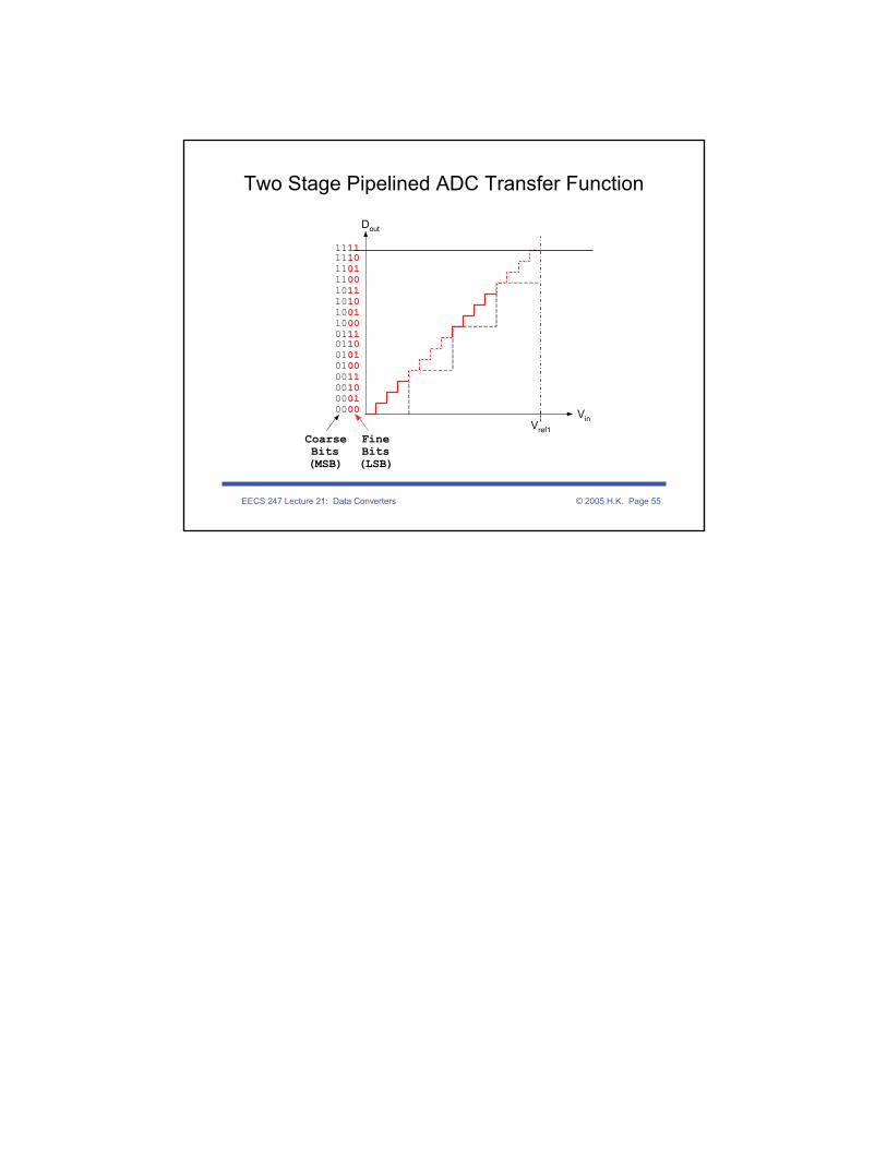
Two Stage Pipelined ADC Transfer Function
Dout
VinVref1
0000000100100011010001010110011110001001101010111100110111101111
CoarseBits(MSB)
FineBits(LSB)