–Higher order ΣΔ modulators - University of California...
36
EECS 247- Lecture 25 Oversampled ADCs © 2009 Page 1 EE247 Lecture 25 Oversampled ADCs (continued) – Higher order ΣΔ modulators • Last lecture Cascaded ΣΔ modulators (MASH) (continued) • Single-loop single-quantizer modulators with multi-order filtering in the forward path – Example: 5 th order Lowpass ΣΔ • Modeling • Noise shaping • Effect of various nonidealities on the ΣΔ performance • Bandpass ΣΔ modulators EECS 247- Lecture 25 Oversampled ADCs © 2009 Page 2 EE247 Lecture 25 •Administrative –Final exam: • Date: Mon. Dec. 14 th • Time: 1:30pm-4:30pm (note change of time) • Location: 299 Cory (change of location) • Closed book/course notes • No calculators/cell phones/PDAs/Computers • You can bring two 8x11 paper with your own notes • Final exam covers the entire course material unless specified
Transcript of –Higher order ΣΔ modulators - University of California...
EECS 247- Lecture 25 Oversampled ADCs © 2009 Page 1
EE247Lecture 25
Oversampled ADCs (continued)– Higher order ΣΔ modulators
• Last lecture Cascaded ΣΔ modulators (MASH) (continued)
• Single-loop single-quantizer modulators with multi-order filtering in the forward path
–Example: 5th order Lowpass ΣΔ • Modeling• Noise shaping• Effect of various nonidealities on the ΣΔ performance
• Bandpass ΣΔ modulators
EECS 247- Lecture 25 Oversampled ADCs © 2009 Page 2
EE247Lecture 25
•Administrative–Final exam:
• Date: Mon. Dec. 14th
• Time: 1:30pm-4:30pm (note change of time)• Location: 299 Cory (change of location)• Closed book/course notes• No calculators/cell phones/PDAs/Computers
• You can bring two 8x11 paper with your own notes• Final exam covers the entire course material unless
specified
EECS 247- Lecture 25 Oversampled ADCs © 2009 Page 3
EE247Lecture 25
Project:– Project reports due Dec. 4th (Dec. 2nd if you are presenting on
Dec. 3rd)– Please make an appointment with the instructor for a 20
minute meeting per team for Frid. Dec. 4th (for early presenters Dec. 2nd)
– Prepare to give a 5 to 10 minute presentation regarding the project during the class period on Dec. 8th (or Dec. 3rd )
• Highlight the important aspects of your approach towards the implementation of the ADC
• If the project is joint effort, both team members should present• Email your PowerPoint presentation files to H.K. two hours prior
to class to conserve class time
EECS 247- Lecture 25 Oversampled ADCs © 2009 Page 4
EE247Lecture 25
• Homework for oversampled data converters– Due to the time consuming nature of the project,
homework covering oversampled converters will not be given. Please review relevant previous year homeworks & solutions e.g.
– http://www-inst.eecs.berkeley.edu/~ee247/fa07/files07/homework/HW9_2_07.pdf
– http://www-inst.eecs.berkeley.edu/~ee247/fa07/files07/homework/HW9_sol_Lynn_Wang.pdf
EECS 247- Lecture 25 Oversampled ADCs © 2009 Page 5
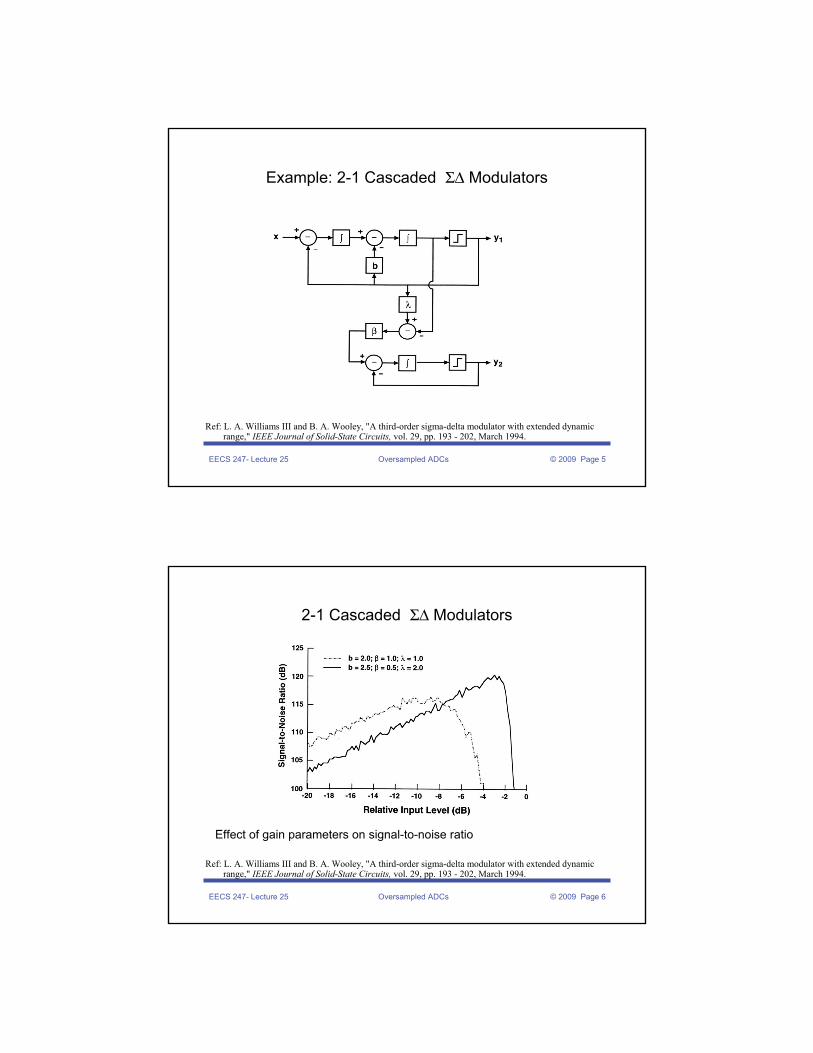
Example: 2-1 Cascaded ΣΔ Modulators
Accuracy of < +−3%2dB loss in DR
Ref: L. A. Williams III and B. A. Wooley, "A third-order sigma-delta modulator with extended dynamic range," IEEE Journal of Solid-State Circuits, vol. 29, pp. 193 - 202, March 1994.
EECS 247- Lecture 25 Oversampled ADCs © 2009 Page 6
2-1 Cascaded ΣΔ Modulators
Effect of gain parameters on signal-to-noise ratio
Ref: L. A. Williams III and B. A. Wooley, "A third-order sigma-delta modulator with extended dynamic range," IEEE Journal of Solid-State Circuits, vol. 29, pp. 193 - 202, March 1994.
EECS 247- Lecture 25 Oversampled ADCs © 2009 Page 7
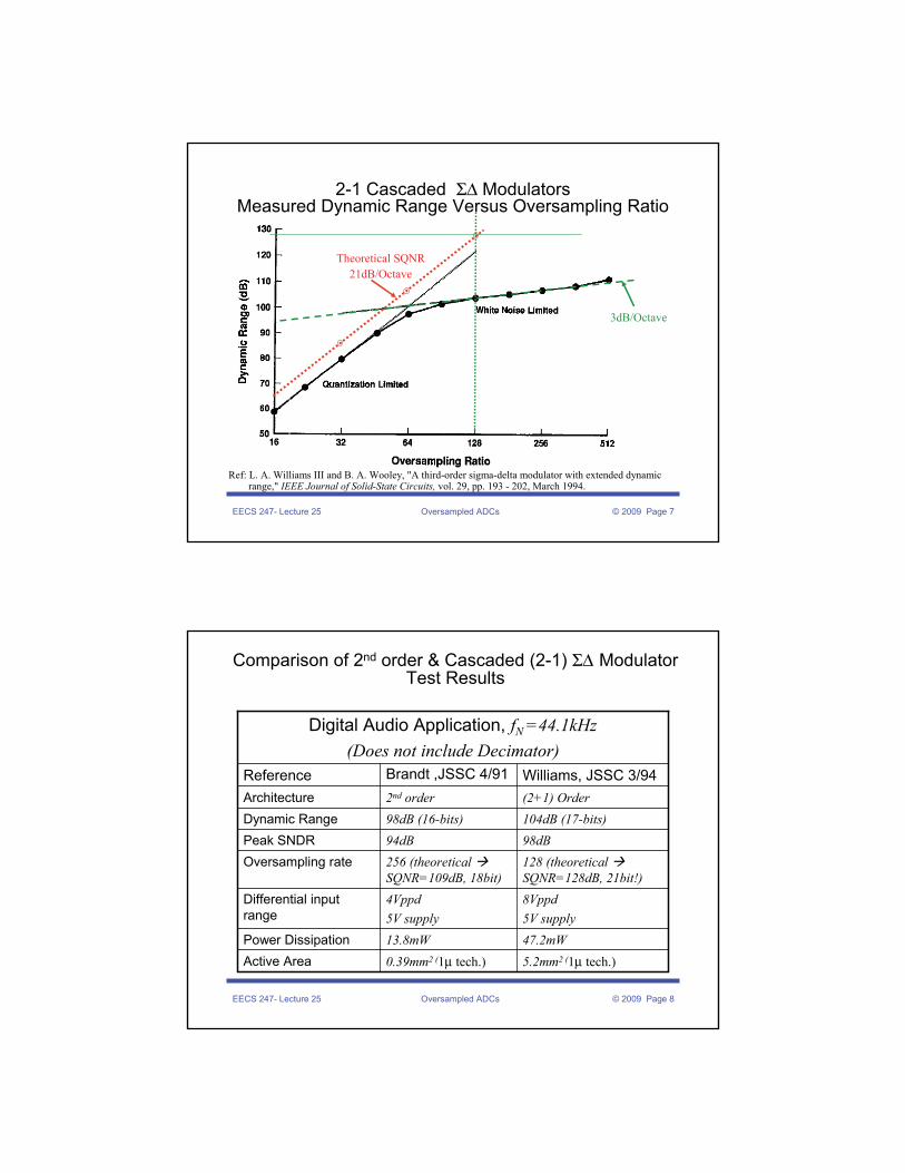
2-1 Cascaded ΣΔ ModulatorsMeasured Dynamic Range Versus Oversampling Ratio
Ref: L. A. Williams III and B. A. Wooley, "A third-order sigma-delta modulator with extended dynamic range," IEEE Journal of Solid-State Circuits, vol. 29, pp. 193 - 202, March 1994.
3dB/Octave
Theoretical SQNR21dB/Octave
EECS 247- Lecture 25 Oversampled ADCs © 2009 Page 8
Comparison of 2nd order & Cascaded (2-1) ΣΔ ModulatorTest Results
5.2mm2 (1μ tech.)0.39mm2 (1μ tech.)Active Area47.2mW13.8mWPower Dissipation
8Vppd5V supply
4Vppd5V supply
Differential input range
128 (theoretical SQNR=128dB, 21bit!)
256 (theoretical SQNR=109dB, 18bit)
Oversampling rate98dB94dBPeak SNDR104dB (17-bits)98dB (16-bits)Dynamic Range(2+1) Order2nd orderArchitectureWilliams, JSSC 3/94Brandt ,JSSC 4/91Reference
Digital Audio Application, fN =44.1kHz(Does not include Decimator)
EECS 247- Lecture 25 Oversampled ADCs © 2009 Page 9
Higher Order ΣΔ Modulators(1) Cascaded Modulators Summary
• Cascade two or more stable ΣΔ stages
• Quantization error of each stage is quantized by the succeeding stage/s and subtracted digitally
• Order of noise shaping equals sum of the orders of the stages
• Quantization noise cancellation depends on the precision of analog/digital signal paths
• Quantization noise further randomized less limit cycle oscillation problems
• Typically, no potential instability
EECS 247- Lecture 25 Oversampled ADCs © 2009 Page 10
Higher Order Lowpass ΣΔ ModulatorsForward Path Multi-Order Filter
• Zeros of NTF (poles of H(z)) can be positioned to minimize baseband noise spectrum
• Main issue Ensuring stability for 3rd and higher orders
( ) 1( ) ( ) ( )1 ( ) 1 ( )
H zY z X z E zH z H z
= ++ +
Σ
E(z)
X(z) Y(z)( )( ) ( )
ND
zH z z= Σ
Y( z ) 1 D( z )NTF =
E( z ) 1 H( z ) D( z ) N( z )= =
+ +
EECS 247- Lecture 25 Oversampled ADCs © 2009 Page 11
Overview• Building behavioral models in stages
• A 5th-order, 1-Bit ΣΔ modulator– Noise shaping – Complex loop filters– Stability– Voltage scaling– Effect of component non-idealities
EECS 247- Lecture 25 Oversampled ADCs © 2009 Page 12
Building Models in Stages• When modeling a complex system like a 5th-order ΣΔ modulator, model
development proceeds in stages– Each stage builds on its predecessor
• Design goal detect and eliminate problems at the highest possible level of abstraction
– Each successive stage consumes progressively more engineering time
• Our ΣΔ model development proceeds in stages:– Stage 0 gets to the starting line: Collect references, talk to veterans– Stage 1 develops a practical system built with ideal sub-circuits & simulation– Stage 2 models key sub-circuit non-idealities and translates the results into
real-world sub-circuit performance specifications – Real-world model development includes a critical stage 3: Adding elements to
earlier stages to model significant surprises found in silicon
EECS 247- Lecture 25 Oversampled ADCs © 2009 Page 13
ΣΔ Modulator Design• Procedure
– Establish requirements– Design noise-transfer function, NTF– Determine loop-filter, H– Synthesize filter– Evaluate performance, – Establish stability criteria
Ref: R. W. Adams and R. Schreier, “Stability Theory for ΔΣ Modulators,” in Delta-Sigma Data Converters- S. Norsworthy et al. (eds), IEEE Press, 1997
EECS 247- Lecture 25 Oversampled ADCs © 2009 Page 14
Example: Modulator Specification
• Example: Audio ADC– Dynamic range DR 18 Bits– Signal bandwidth B 20 kHz– Nyquist frequency fN 44.1 kHz– Modulator order L 5– Oversampling ratio M = fs/fN 64– Sampling frequency fs 2.822 MHz
• The order L and oversampling ratio M are chosen based on– SQNR > 120dB
EECS 247- Lecture 25 Oversampled ADCs © 2009 Page 15
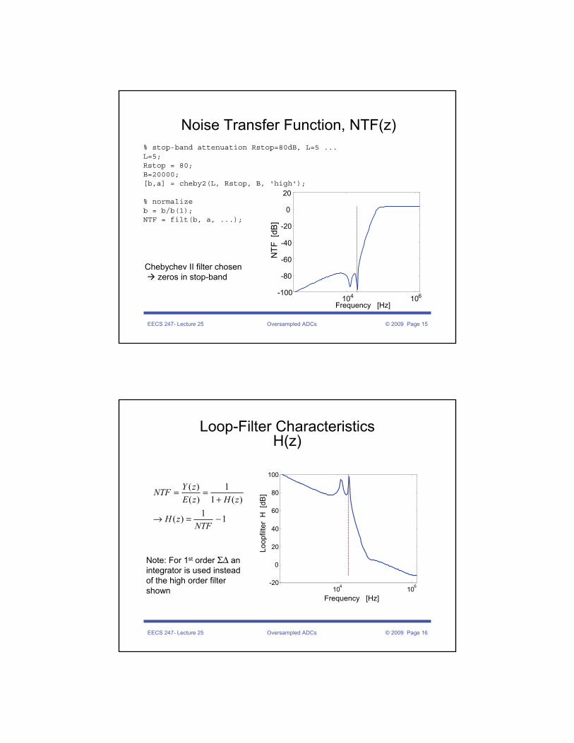
Noise Transfer Function, NTF(z)% stop-band attenuation Rstop=80dB, L=5 ... L=5; Rstop = 80;B=20000; [b,a] = cheby2(L, Rstop, B, 'high');
% normalize b = b/b(1); NTF = filt(b, a, ...);
104 106-100
-80
-60
-40
-20
0
20
Frequency [Hz]
NTF
[dB
]Chebychev II filter chosen
zeros in stop-band
EECS 247- Lecture 25 Oversampled ADCs © 2009 Page 16
Loop-Filter CharacteristicsH(z)
( ) 1( ) 1 ( )
1( ) 1
Y zNTFE z H z
H zNTF
= =+
→ = −
104 106-20
0
20
40
60
80
100
Frequency [Hz]
Loop
filte
r H
[dB
]
Note: For 1st order ΣΔ an integrator is used instead of the high order filter shown
EECS 247- Lecture 25 Oversampled ADCs © 2009 Page 17
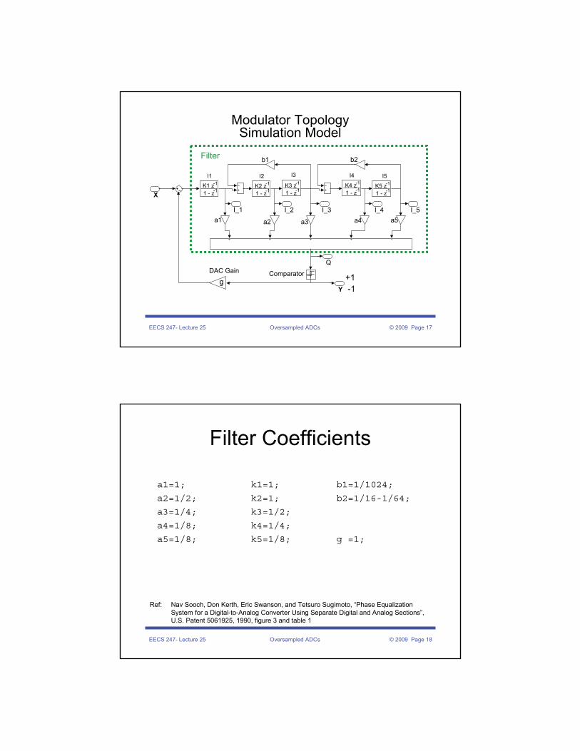
Modulator TopologySimulation Model
Q
I_5I_4I_3I_2I_1
Y
b2b1
a5a4a3a2a1
K1 z -1
1 - z -1
I1
DAC Gain Comparator
X
-1
1 - z -1
I2
K2 z -1
1 - z -1
I3
K3 z -1
1 - z -1
I4
K4 z -1
1 - z -1
I5
K5 z
+1-1
Filter
g
EECS 247- Lecture 25 Oversampled ADCs © 2009 Page 18
Filter Coefficients
a1=1;
a2=1/2;
a3=1/4;
a4=1/8;
a5=1/8;
k1=1;
k2=1;
k3=1/2;
k4=1/4;
k5=1/8;
b1=1/1024;
b2=1/16-1/64;
g =1;
Ref: Nav Sooch, Don Kerth, Eric Swanson, and Tetsuro Sugimoto, “Phase Equalization System for a Digital-to-Analog Converter Using Separate Digital and Analog Sections”, U.S. Patent 5061925, 1990, figure 3 and table 1
EECS 247- Lecture 25 Oversampled ADCs © 2009 Page 19
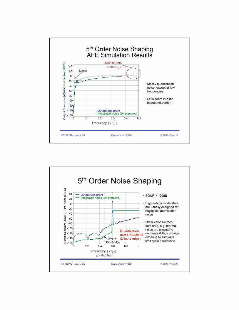
5th Order Noise ShapingAFE Simulation Results
• Mostly quantization noise, except at low frequencies
• Let’s zoom into the baseband portion…
0 0.1 0.2 0.3 0.4 0.5-160
-140
-120
-100
-80
-60
-40
-20
0
20
40
Frequency [ f / fs ]
Out
put S
pect
rum
[dB
WN
]/ In
t. N
oise
[dB
FS]
Output SpectrumIntegrated Noise (20 averages)
Signal
Notice tones around fs/2
EECS 247- Lecture 25 Oversampled ADCs © 2009 Page 20
5th Order Noise Shaping
0 0.2 0.4 0.6 0.8 1-160
-140
-120
-100
-80
-60
-40
-20
0
20
40
Out
put S
pect
rum
[dB
WN
] /
Int.
Noi
se [d
BFS
]
Output SpectrumIntegrated Noise (20 averaged)
Quantization noise -130dBFS @ band edge!Signal
Band-Edge
Frequency [ f / fN ] fN =44.1kHz
• SQNR > 120dB
• Sigma-delta modulators are usually designed for negligible quantization noise
• Other error sources dominate, e.g. thermal noise are allowed to dominate & thus provide dithering to eliminate limit cycle oscillations
EECS 247- Lecture 25 Oversampled ADCs © 2009 Page 21
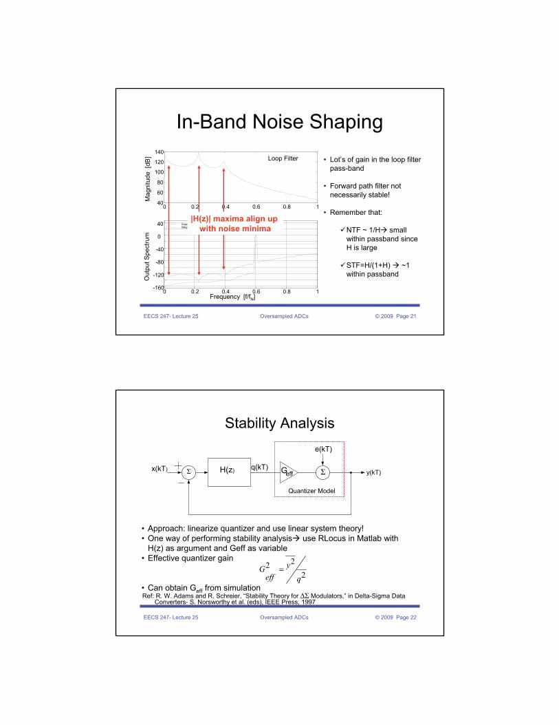
0 0.2 0.4 0.6 0.8 140
60
80
100
120
140M
agni
tude
[dB
] Loop Filter
0 0.2 0.4 0.6 0.8 1-100
0
100
200
300
400
Frequency [f/fN]
Phas
e [d
egre
es]
In-Band Noise Shaping• Lot’s of gain in the loop filter
pass-band
• Forward path filter not necessarily stable!
• Remember that:
NTF ~ 1/H small within passband since H is large
STF=H/(1+H) ~1 within passband
0 0.2 0.4 0.6 0.8 1-160
-120
-80
-40
0
40
Frequency [f/fN]
Out
put S
pect
rum
Output SpectrumIntegrated Noise (20 averages)
|H(z)| maxima align up with noise minima
EECS 247- Lecture 25 Oversampled ADCs © 2009 Page 22
Stability Analysis
• Approach: linearize quantizer and use linear system theory!• One way of performing stability analysis use RLocus in Matlab with
H(z) as argument and Geff as variable• Effective quantizer gain
• Can obtain Geff from simulation
222
yGeff q
=
H(z)Σ Σ
Quantizer Model
e(kT)
x(kT) y(kT)Geffq(kT)
Ref: R. W. Adams and R. Schreier, “Stability Theory for ΔΣ Modulators,” in Delta-Sigma Data Converters- S. Norsworthy et al. (eds), IEEE Press, 1997
EECS 247- Lecture 25 Oversampled ADCs © 2009 Page 23
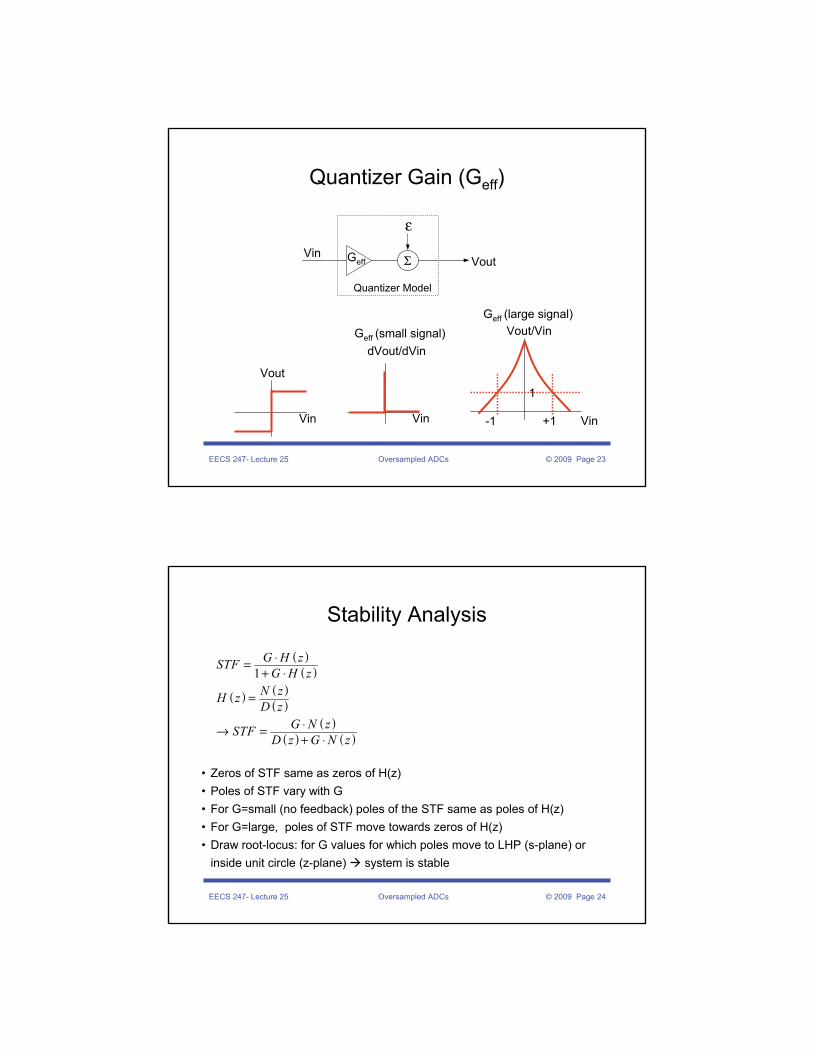
Quantizer Gain (Geff)
Σ
Quantizer Model
ε
VoutGeffVin
Geff (large signal)
Vout
Vin -1 +1
1
Vin
Geff (small signal) Vout/Vin
dVout/dVin
Vin
EECS 247- Lecture 25 Oversampled ADCs © 2009 Page 24
Stability Analysis
• Zeros of STF same as zeros of H(z)• Poles of STF vary with G• For G=small (no feedback) poles of the STF same as poles of H(z)• For G=large, poles of STF move towards zeros of H(z)• Draw root-locus: for G values for which poles move to LHP (s-plane) or
inside unit circle (z-plane) system is stable
( )( )
( ) ( )( )
( )( ) ( )
1G H zSTF
G H zN zH zD z
G N zSTFD z G N z
⋅=+ ⋅
=
⋅→ =+ ⋅
EECS 247- Lecture 25 Oversampled ADCs © 2009 Page 25
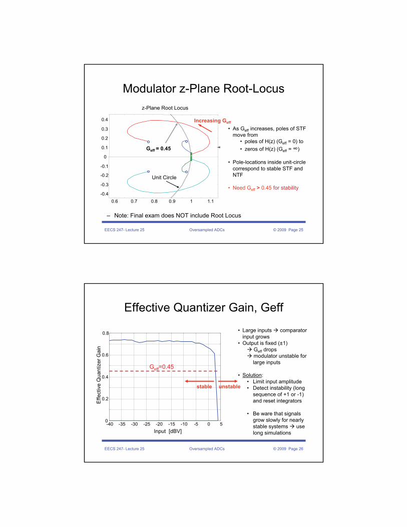
Modulator z-Plane Root-Locus
• As Geff increases, poles of STF move from
• poles of H(z) (Geff = 0) to • zeros of H(z) (Geff = ∞)
• Pole-locations inside unit-circle correspond to stable STF and NTF
• Need Geff > 0.45 for stability
Geff = 0.45
z-Plane Root Locus
0.6 0.7 0.8 0.9 1 1.1-0.4
-0.3
-0.2
-0.1
0
0.1
0.2
0.3
0.4 Increasing Geff
Unit Circle
– Note: Final exam does NOT include Root Locus
EECS 247- Lecture 25 Oversampled ADCs © 2009 Page 26
-40 -35 -30 -25 -20 -15 -10 -5 0 50
0.2
0.4
0.6
0.8
Input [dBV]
Effe
ctiv
e Q
uant
izer
Gai
n
Geff=0.45
stable unstable
• Large inputs comparator input grows
• Output is fixed (±1)Geff dropsmodulator unstable for large inputs
• Solution:• Limit input amplitude• Detect instability (long
sequence of +1 or -1) and reset integrators
• Be ware that signals grow slowly for nearly stable systems use long simulations
Effective Quantizer Gain, Geff
EECS 247- Lecture 25 Oversampled ADCs © 2009 Page 27
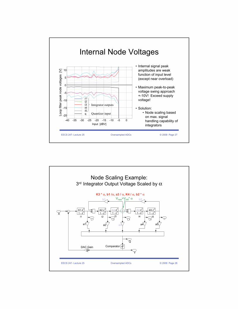
-40 -35 -30 -25 -20 -15 -10 -5 0
-20
-15
-10
-5
0
5
10
i1i2i3i4i5q
Input [dBV]
Loop
filte
r pea
k no
de v
olta
ges
[V]
Internal Node Voltages• Internal signal peak
amplitudes are weak function of input level (except near overload)
• Maximum peak-to-peak voltage swing approach +-10V! Exceed supply voltage!
• Solution:• Node scaling based
on max. signal handling capability of integrators
Integrator outputs
Quantizer input
EECS 247- Lecture 25 Oversampled ADCs © 2009 Page 28
Node Scaling Example:3rd Integrator Output Voltage Scaled by α
K3 * α, b1 /α, a3 / α, K4 / α, b2 * αVnew=Vold* α
Q
I_5I_4I_3I_2I_1
Y
b2b1
a5a4a3a2a1
K1 z -1
1 - z -1
I1
gDAC Gain Comparator
X
-1
1 - z -1
I2
K2 z -1
1 - z -1
I3
K3 z -1
1 - z -1
I4
K4 z -1
1 - z -1
I5
K5 z
EECS 247- Lecture 25 Oversampled ADCs © 2009 Page 29
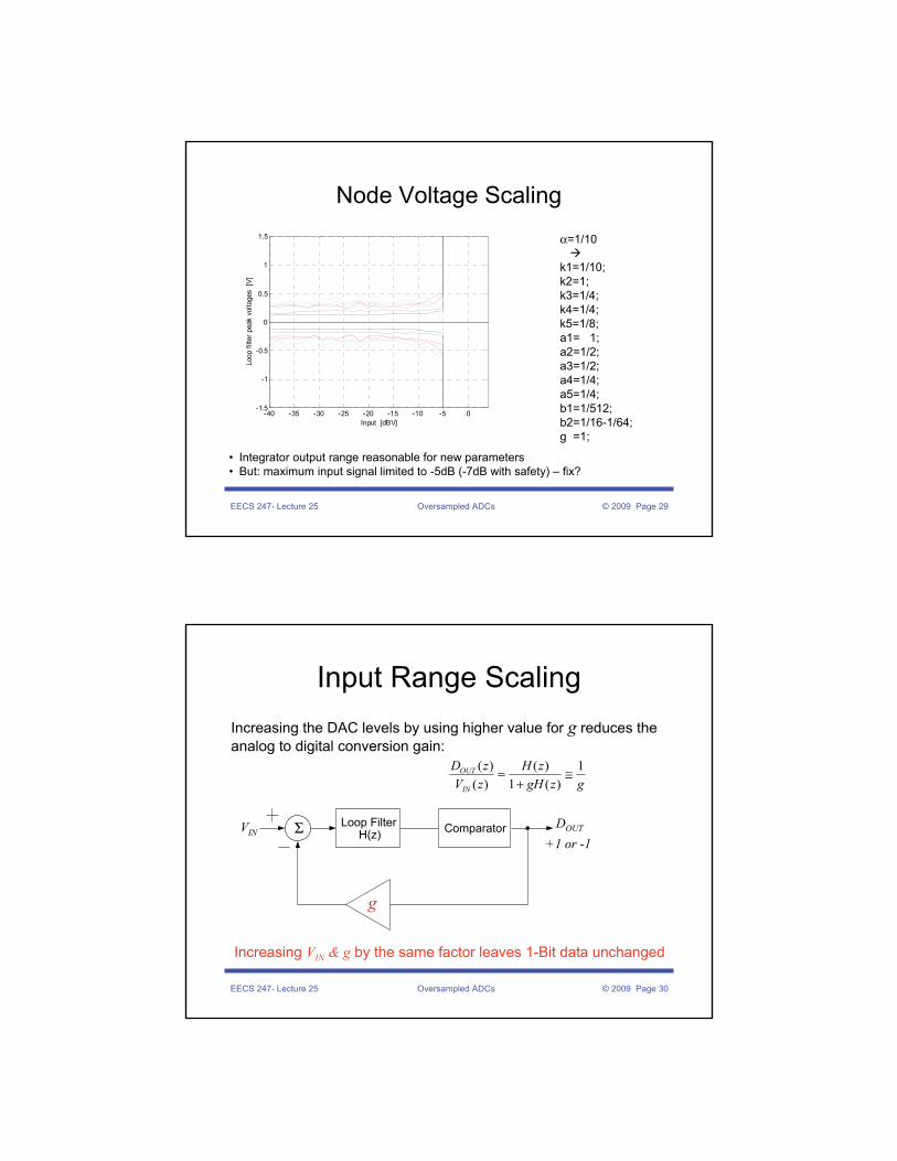
Node Voltage Scaling
-40 -35 -30 -25 -20 -15 -10 -5 0-1.5
-1
-0.5
0
0.5
1
1.5
Input [dBV]
Loop
filte
r pea
k vo
ltage
s [V
]α=1/10
k1=1/10;k2=1;k3=1/4;k4=1/4;k5=1/8;a1= 1; a2=1/2;a3=1/2; a4=1/4;a5=1/4;b1=1/512;b2=1/16-1/64;g =1;
• Integrator output range reasonable for new parameters• But: maximum input signal limited to -5dB (-7dB with safety) – fix?
EECS 247- Lecture 25 Oversampled ADCs © 2009 Page 30
Input Range ScalingIncreasing the DAC levels by using higher value for g reduces the analog to digital conversion gain:
Increasing VIN & g by the same factor leaves 1-Bit data unchanged
gzgHzH
zVzD
IN
OUT 1)(1
)()()( ≅
+=
Loop FilterH(z)ΣVIN
DOUT
+1 or -1Comparator
g
EECS 247- Lecture 25 Oversampled ADCs © 2009 Page 31
Scaled Stage 1 Model
g modified:From 1 to 2.5;
Overload input level shifted up by 8dB
-40 -35 -30 -25 -20 -15 -10 -5 0-1.5
-1
-0.5
0
0.5
1
1.5
Input [dBV]
Loop
filte
r pea
k vo
ltage
s [V
]
+2dB
EECS 247- Lecture 25 Oversampled ADCs © 2009 Page 32
Scaled Stage 1 Model
g = 2.5;
-40 -35 -30 -25 -20 -15 -10 -5 0-1.5
-1
-0.5
0
0.5
1
1.5
Input [dBV]
Loop
filte
r pea
k vo
ltage
s [V
]
EECS 247- Lecture 25 Oversampled ADCs © 2009 Page 33
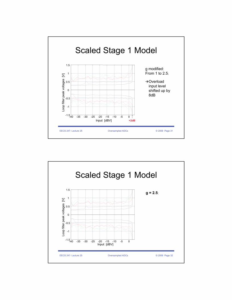
Stability VerificationPost Scaling
Note: Operating the AFE at signals <0dBV ensures system stability
-40 -35 -30 -25 -20 -15 -10 -5 0 50
1
2
3
4
5
6
7
8
Input [dBV]
Effe
ctiv
e Q
uant
izer
Gai
n
Geff=4.5stable unstable
EECS 247- Lecture 25 Oversampled ADCs © 2009 Page 34
5th Order ModulatorFinal Parameter Values
±2.5V
Stable input range with margin ~ ±1V
1/10 1 1/4 1/4 1/8
1/512 1/16-1/64
1 12 1/2 1/4 1/4
Input range~ ±1V
Q
I_5I_4I_3I_2I_1
Y
b2b1
a5a4a3a2a1
K1 z -1
1 - z -1
I1
gDAC Gain Comparator
X
-1
1 - z -1
I2
K2 z -1
1 - z -1
I3
K3 z -1
1 - z -1
I4
K4 z -1
1 - z -1I5
K5 z
1
EECS 247- Lecture 25 Oversampled ADCs © 2009 Page 35
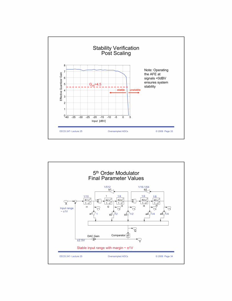
Summary
• Stage 1 model verified –stable and meets SQNR specification
• Stage 2 issues in 5th order ΣΔ modulator– DC inputs– Spurious tones– Dither– kT/C noise
EECS 247- Lecture 25 Oversampled ADCs © 2009 Page 36
0 0.5 1 1.5-150
-100
-50
0
50
Frequency [MHz]
Out
put S
pect
rum
[dB
WN
] /
Int.
Noi
se [d
BV
]
Output SpectrumIntegrated Noise (30 averages)
5th Order Noise Shaping
Input: 0.1V, sinusoid215 point DFT30 averages
Note: Large spurious tonesin the vicinity of fs/2
Let us check whether tones appear inband?
Tones in the vicinity of fs/2 exceed input level
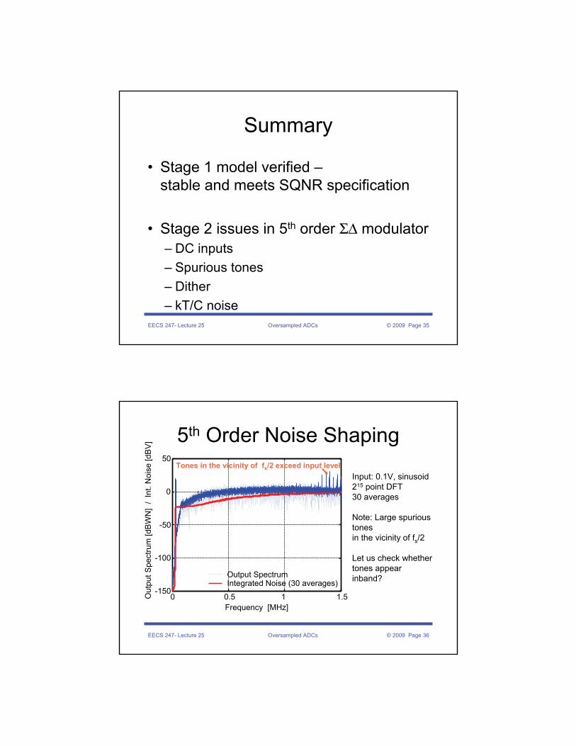
EECS 247- Lecture 25 Oversampled ADCs © 2009 Page 37
0 10 20 30 40 50-150
-100
-50
0
50
Frequency [kHz]
Out
put S
pect
rum
[dB
WN
] /
Int.
Noi
se [d
BV
]Output SpectrumIntegrated Noise (30 averages)
In-Band Noise
In-Band quantization noise:–120dB !
Note: No in-band tones!While Large spurious tones appear in the vicinity of fs /2
EECS 247- Lecture 25 Oversampled ADCs © 2009 Page 38
0 0.5 1 1.5-150
-100
-50
0
50
Frequency [MHz]
Out
put S
pect
rum
[dB
WN
] /
Int.
Noi
se [d
BV
]
Output SpectrumIntegrated Noise (30 averages)
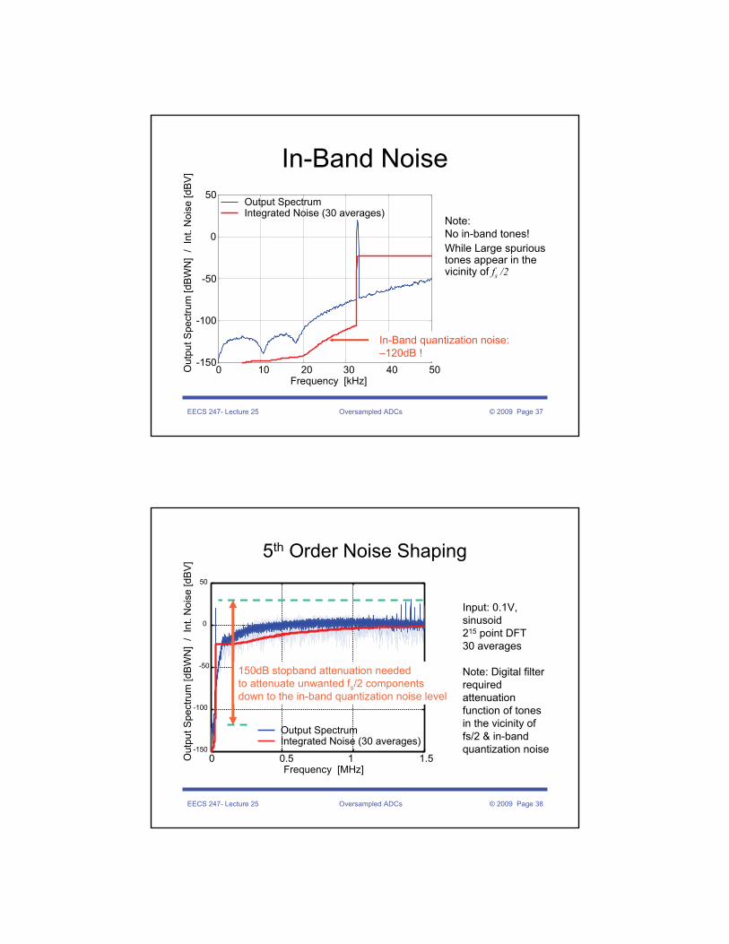
5th Order Noise Shaping
Input: 0.1V, sinusoid215 point DFT30 averages
Note: Digital filter required attenuation function of tones in the vicinity of fs/2 & in-band quantization noise
150dB stopband attenuation neededto attenuate unwanted fs/2 componentsdown to the in-band quantization noise level
EECS 247- Lecture 25 Oversampled ADCs © 2009 Page 39
Out-of-Band vs In-Band Signals
• A digital (low-pass) filter with suitable coefficient precision can eliminate out-of-band quantization noise
• No filter can attenuate unwanted in-band components without attenuating the signal
• We’ll spend some time making sure the components at fs/2-fin will not “mix” down to the signal band
• But first, let’s look at the modulator response to small DC inputs (or offset) …
EECS 247- Lecture 25 Oversampled ADCs © 2009 Page 40
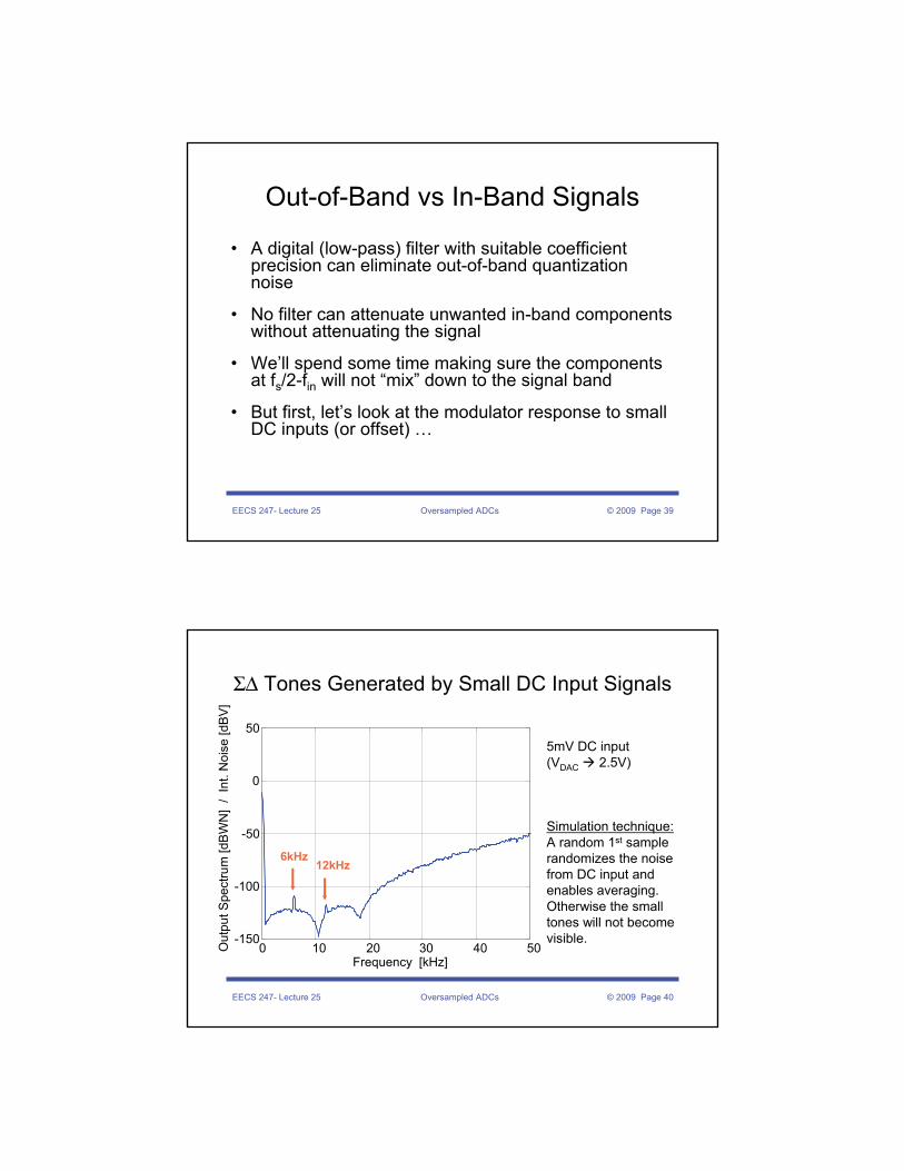
ΣΔ Tones Generated by Small DC Input Signals
5mV DC input(VDAC 2.5V)
Simulation technique:A random 1st sample randomizes the noise from DC input and enables averaging. Otherwise the small tones will not become visible.
0 10 20 30 40 50-150
-100
-50
0
50
Frequency [kHz]
Out
put S
pect
rum
[dB
WN
] /
Int.
Noi
se [d
BV
]
6kHz12kHz
EECS 247- Lecture 25 Oversampled ADCs © 2009 Page 41
Limit Cycles
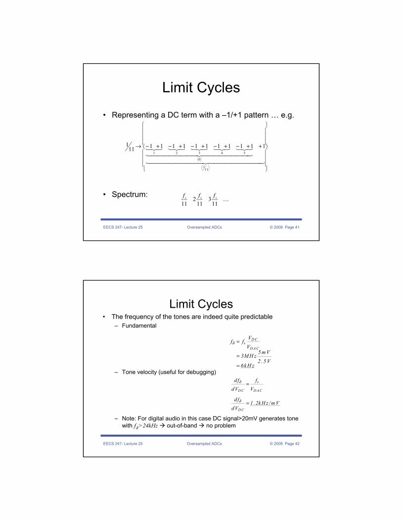
• Representing a DC term with a –1/+1 pattern … e.g.
• Spectrum:
⎪⎪⎪
⎭
⎪⎪⎪
⎬
⎫
⎪⎪⎪
⎩
⎪⎪⎪
⎨
⎧
++−+−+−+−+−→
444444444 3444444444 21
44444444 344444444 21321321321321321
111
0
54321
1 1 1 1 1 1 1 1 1 1 1111
K11
311
211
sss fff
EECS 247- Lecture 25 Oversampled ADCs © 2009 Page 42
Limit Cycles• The frequency of the tones are indeed quite predictable
– Fundamental
– Tone velocity (useful for debugging)
– Note: For digital audio in this case DC signal>20mV generates tone with fδ >24kHz out-of-band no problem
D Cs
D A C
Vf f
V5 m V
3M H z2 .5 V
6k H z
δ =
=
=
s
D C D A C
D C
d f fd V V
d f1 .2k H z /m V
d V
δ
δ
=
=
EECS 247- Lecture 25 Oversampled ADCs © 2009 Page 43
1.47 1.48 1.49 1.5-150
-100
-50
0
50
Frequency [MHz]
Out
put S
pect
rum
[dB
WN
] /
Int.
Noi
se [d
BV
]
Output SpectrumIntegrated Noise (30 averages)
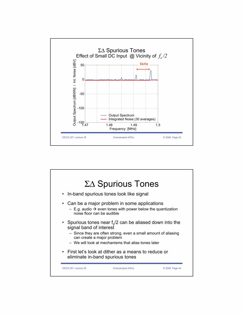
ΣΔ Spurious TonesEffect of Small DC Input @ Vicinity of fs /2
6kHz
EECS 247- Lecture 25 Oversampled ADCs © 2009 Page 44
ΣΔ Spurious Tones• In-band spurious tones look like signal
• Can be a major problem in some applications– E.g. audio even tones with power below the quantization
noise floor can be audible
• Spurious tones near fs/2 can be aliased down into the signal band of interest– Since they are often strong, even a small amount of aliasing
can create a major problem– We will look at mechanisms that alias tones later
• First let’s look at dither as a means to reduce or eliminate in-band spurious tones
EECS 247- Lecture 25 Oversampled ADCs © 2009 Page 45
Dither
• DC inputs can be represented by many possible bit patterns
• Including some that are random (non-periodic) but still average to the desired DC input
• The spectrum of such a sequence has no spurious tones
• How can we get a ΣΔ modulator to produce such “randomized” sequences?
EECS 247- Lecture 25 Oversampled ADCs © 2009 Page 46
Dither
• The target DR for our audio ΣΔ is 18 Bits, or 113dB• Designed SQNR~-120dB allows thermal noise to
dominate at -115dB level• Let’s choose the sampling capacitor such that it limits
the dynamic range:( )
( )
212
2
2 12
1
1μV
FSFS
n
n FSDR
VDR V Vp
v
v V
= =
→ = =
EECS 247- Lecture 25 Oversampled ADCs © 2009 Page 47
5mV DC input
• Thermal noise added at the input of the 1st
integrator
• In-band spurious tones disappear
• Note: they are not just buried
• How can we tell?0 10 20 30 40 50-150
-100
-50
0
50
Frequency [kHz]
Out
put S
pect
rum
[dBW
N]
No ditherWith dither (thermal noise)
Effect of Dither on In-Band Spurious Tones
EECS 247- Lecture 25 Oversampled ADCs © 2009 Page 48
Effect of Dither on Spurious Tones Near fs/2
Key point: Dither at an amplitude which eliminate the in-band tones has virtually no effect on tones near fs/2
1.47 1.48 1.49 1.5-150
-100
-50
0
50
Frequency [MHz]
Out
put S
pect
rum
[dB
WN
]
No ditherWith dither
EECS 247- Lecture 25 Oversampled ADCs © 2009 Page 49
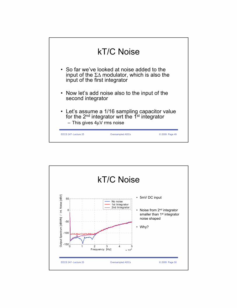
kT/C Noise
• So far we’ve looked at noise added to the input of the ΣΔ modulator, which is also the input of the first integrator
• Now let’s add noise also to the input of the second integrator
• Let’s assume a 1/16 sampling capacitor value for the 2nd integrator wrt the 1st integrator– This gives 4μV rms noise
EECS 247- Lecture 25 Oversampled ADCs © 2009 Page 50
kT/C Noise
• 5mV DC input
• Noise from 2nd integrator smaller than 1st integrator noise shaped
• Why?
0 1 2 3 4 5x 10⁴
-150
-100
-50
0
50
Frequency [Hz]
Out
put S
pect
rum
[dB
WN
] /
Int.
Noi
se [d
BV]
No noise1st Integrator2nd In tegrator
EECS 247- Lecture 25 Oversampled ADCs © 2009 Page 51
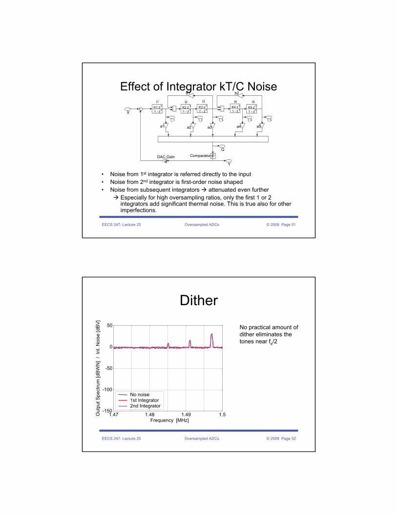
Effect of Integrator kT/C Noise
• Noise from 1st integrator is referred directly to the input• Noise from 2nd integrator is first-order noise shaped• Noise from subsequent integrators attenuated even further
Especially for high oversampling ratios, only the first 1 or 2 integrators add significant thermal noise. This is true also for other imperfections.
Q
I_5I_4I_3I_2I_1
Y
b2b1
a5a4a3a2a1
K1 z -1
1 - z -1
I1
gDAC Gain Comparator
X
-1
1 - z -1
I2
K2 z -1
1 - z -1
I3
K3 z -1
1 - z -1
I4
K4 z -1
1 - z -1
I5
K5 z
EECS 247- Lecture 25 Oversampled ADCs © 2009 Page 52
Dither
No practical amount of dither eliminates the tones near fs/2
1.47 1.48 1.49 1.5-150
-100
-50
0
50
Frequency [MHz]
Out
put S
pect
rum
[dBW
N]
/ In
t. N
oise
[dBV
]
No noise1st Integrator2nd Integrator
EECS 247- Lecture 25 Oversampled ADCs © 2009 Page 53
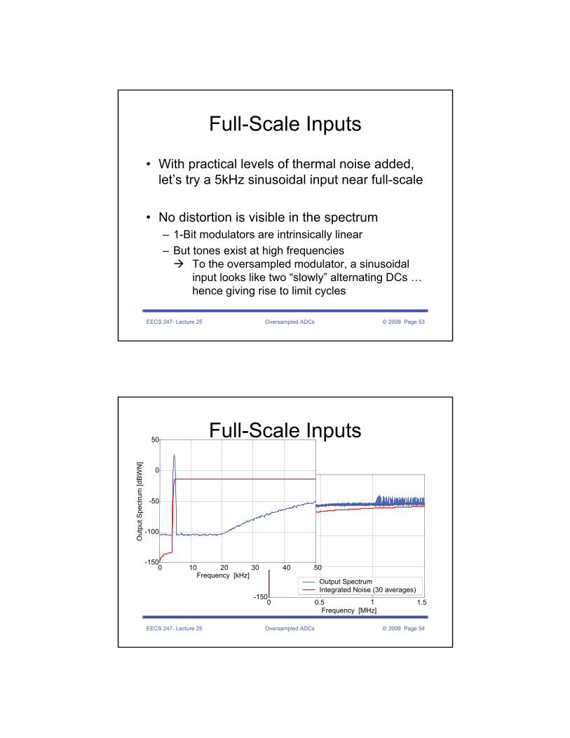
Full-Scale Inputs
• With practical levels of thermal noise added, let’s try a 5kHz sinusoidal input near full-scale
• No distortion is visible in the spectrum– 1-Bit modulators are intrinsically linear– But tones exist at high frequencies
To the oversampled modulator, a sinusoidalinput looks like two “slowly” alternating DCs …hence giving rise to limit cycles
EECS 247- Lecture 25 Oversampled ADCs © 2009 Page 54
0 0.5 1 1.5-150
-100
-50
0
50
Frequency [MHz]
Out
put S
pect
rum
[dBW
N]
Output SpectrumIntegrated Noise (30 averages)
Full-Scale Inputs
0 10 20 30 40 50-150
-100
-50
0
50
Frequency [kHz]
Out
put S
pect
rum
[dBW
N]
EECS 247- Lecture 25 Oversampled ADCs © 2009 Page 55
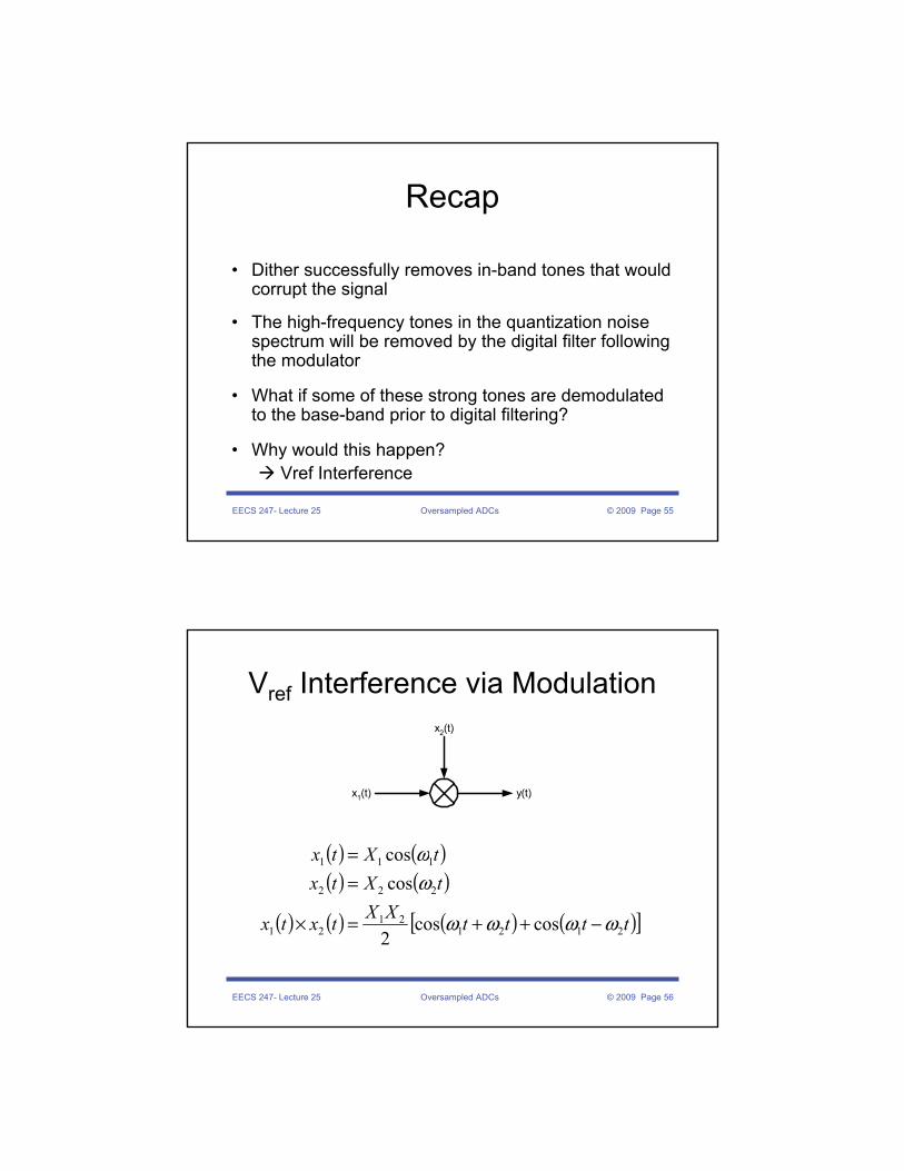
Recap
• Dither successfully removes in-band tones that would corrupt the signal
• The high-frequency tones in the quantization noise spectrum will be removed by the digital filter following the modulator
• What if some of these strong tones are demodulated to the base-band prior to digital filtering?
• Why would this happen?Vref Interference
EECS 247- Lecture 25 Oversampled ADCs © 2009 Page 56
Vref Interference via Modulationx2(t)
x1(t) y(t)
( ) ( )( ) ( )
( ) ( ) ( ) ( )[ ]ttttXXtxtx
tXtxtXtx
212121
21
222
111
coscos2
coscos
ωωωω
ωω
−++=×
==
EECS 247- Lecture 25 Oversampled ADCs © 2009 Page 57
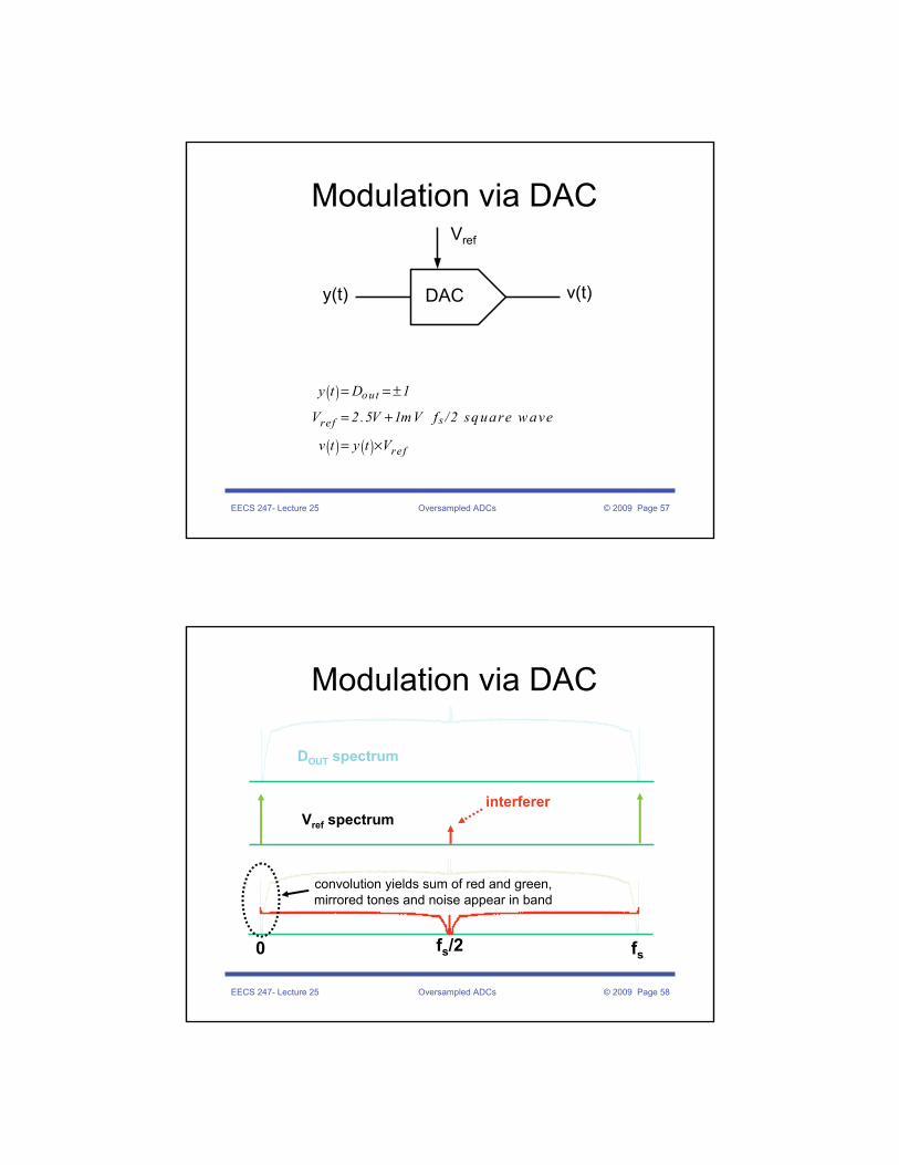
Modulation via DAC
DACy(t) v(t)
Vref
( )
( ) ( )
out
sref
ref
y t D 1
V 2.5V 1mV f /2 square w ave
v t y t V
= = ±
= +
= ×
EECS 247- Lecture 25 Oversampled ADCs © 2009 Page 58
Modulation via DAC
0 fs/2 fs
DOUT spectrum
Vref spectruminterferer
convolution yields sum of red and green,mirrored tones and noise appear in band
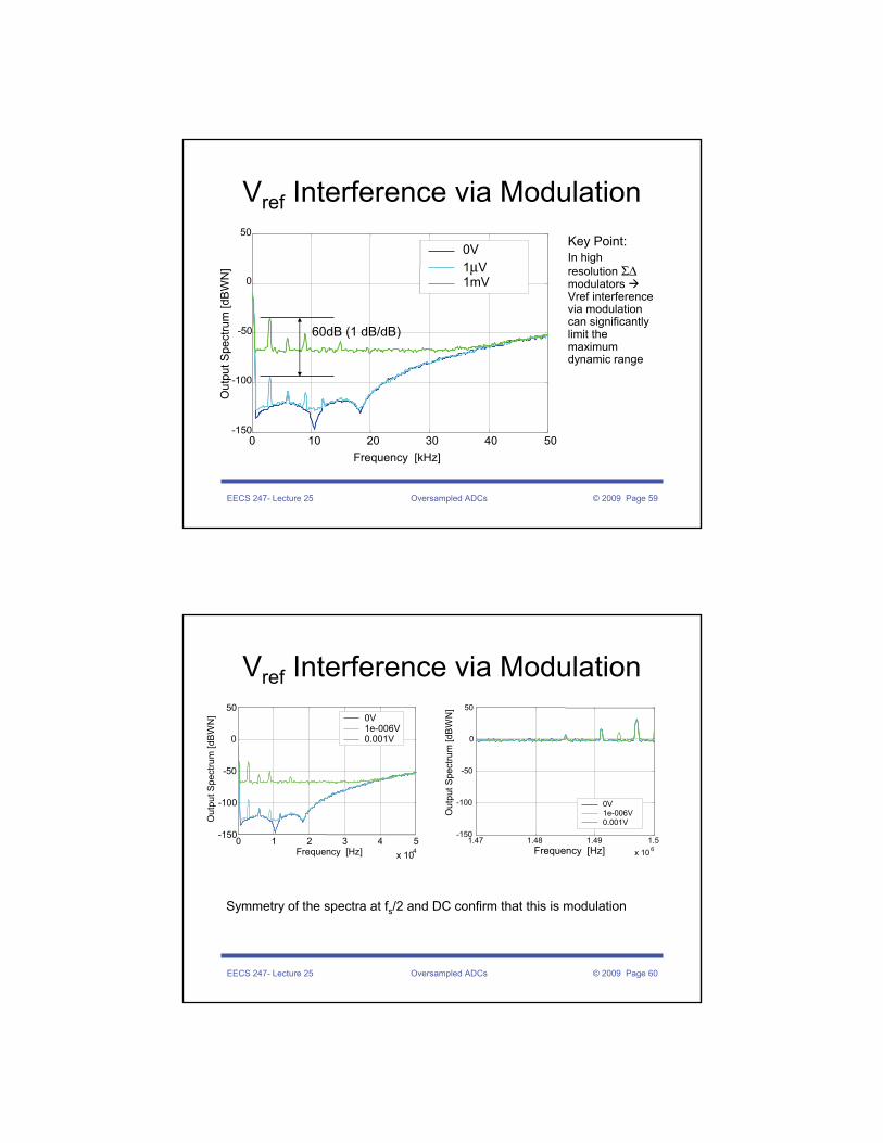
EECS 247- Lecture 25 Oversampled ADCs © 2009 Page 59
0 10 20 30 40 50-150
-100
-50
0
50
Frequency [kHz]
Out
put S
pect
rum
[dB
WN
]
0V1μV1mV
60dB (1 dB/dB)
Vref Interference via ModulationKey Point:In high resolution ΣΔmodulators Vref interference via modulation can significantly limit the maximum dynamic range
EECS 247- Lecture 25 Oversampled ADCs © 2009 Page 60
Symmetry of the spectra at fs/2 and DC confirm that this is modulation
1.47 1.48 1.49 1.5x 10 6
-150
-100
-50
0
50
Frequency [Hz]
Out
put S
pect
rum
[dB
WN
]
0V1e-006V0.001V
0 1 2 3 4 5x 10⁴
-150
-100
-50
0
50
Frequency [Hz]
Out
put S
pect
rum
[dB
WN
] 0V1e-006V0.001V
Vref Interference via Modulation
EECS 247- Lecture 25 Oversampled ADCs © 2009 Page 61
0 10 20 30 40 50-150
-100
-50
0
50
Frequency [kHz]
Out
put S
pect
rum
[dB
WN
]0.006V0.012V
Vref Spurious Tone Velocity vs Native Tone Velocity
0.6kHz/mV
Vin = 6mV / 12mV DCVref = 2.5V DC
& 1mV fs/2
40dB shift for readability
Native tone
Aliased tone
• Native tone velocity
1.2kHz/mV
• Aliased tone velocity
0.6kHz/mV
EECS 247- Lecture 25 Oversampled ADCs © 2009 Page 62
• Simulations performed to verify the effect of the DAC referencecontamination via output signal interference particularly in the vicinity of fs /2
• Interference modulates the high-frequency tones
• Since the high frequency tones are strong, a small amount (1μV) of interference suffices to create audible base-band tones
• Stronger interference (1mV) not only aliases spurious tones but elevated raises noise floor by aliasing high frequency quantization noise
• Amplitude of modulated tones is proportional to interference
• The velocity of modulated tones is half that of the native tones
• Such differences could help debugging of silicon
• How clean does the reference have to be?
Vref Interference via Modulation
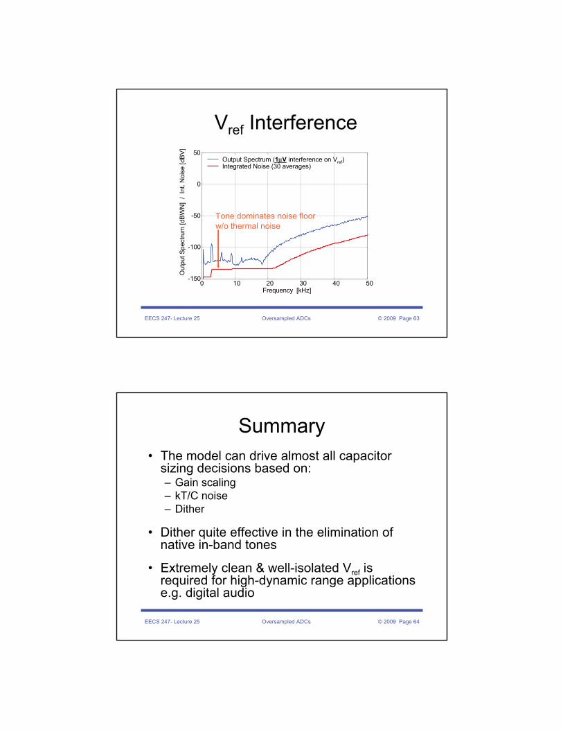
EECS 247- Lecture 25 Oversampled ADCs © 2009 Page 63
0 10 20 30 40 50-150
-100
-50
0
50
Frequency [kHz]
Out
put S
pect
rum
[dB
WN
] /
Int.
Noi
se [d
BV]
Output Spectrum (1μV interference on Vref)Integrated Noise (30 averages)
Vref Interference
Tone dominates noise floorw/o thermal noise
EECS 247- Lecture 25 Oversampled ADCs © 2009 Page 64
Summary• The model can drive almost all capacitor
sizing decisions based on:– Gain scaling– kT/C noise– Dither
• Dither quite effective in the elimination of native in-band tones
• Extremely clean & well-isolated Vref is required for high-dynamic range applications e.g. digital audio
EECS 247- Lecture 25 Oversampled ADCs © 2009 Page 65
Bandpass ΔΣ Modulator
+
_vIN
dOUT
∫
DAC
• Replace the integrator in 1st order lowpass ΣΔ with a resonator
2nd order bandpass ΣΔ
Resonator
∫
∫
EECS 247- Lecture 25 Oversampled ADCs © 2009 Page 66
Bandpass ΔΣ ModulatorExample: 6th Order
Measured output for a bandpass ΣΔ (prior to digital filtering)
Key Point:
NTF notch type shape
STF bandpass shape
Ref: Paolo Cusinato, et. al, “A 3.3-V CMOS 10.7-MHz Sixth-Order Bandpass Modulator with 74-dB Dynamic Range “, ΙΕΕΕ JSSCC, VOL. 36, NO. 4, APRIL 2001
Input SinusoidQuantization Noise
EECS 247- Lecture 25 Oversampled ADCs © 2009 Page 67
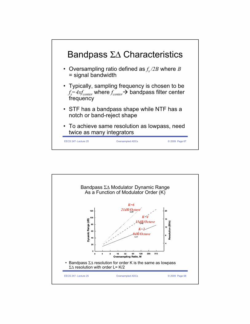
Bandpass ΣΔ Characteristics• Oversampling ratio defined as fs /2B where B
= signal bandwidth
• Typically, sampling frequency is chosen to be fs=4xfcenter where fcenter bandpass filter center frequency
• STF has a bandpass shape while NTF has a notch or band-reject shape
• To achieve same resolution as lowpass, need twice as many integrators
EECS 247- Lecture 25 Oversampled ADCs © 2009 Page 68
Bandpass ΣΔ Modulator Dynamic RangeAs a Function of Modulator Order (K)
• Bandpass ΣΔ resolution for order K is the same as lowpass ΣΔ resolution with order L= K/2
K=415dB/Octave
K=621dB/Octave
K=29dB/Octave
EECS 247- Lecture 25 Oversampled ADCs © 2009 Page 69
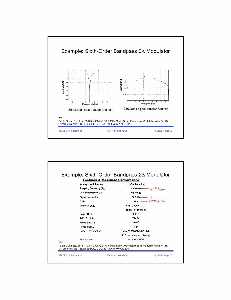
Example: Sixth-Order Bandpass ΣΔ Modulator
Ref: Paolo Cusinato, et. al, “A 3.3-V CMOS 10.7-MHz Sixth-Order Bandpass Modulator with 74-dB Dynamic Range “, ΙΕΕΕ JSSCC, VOL. 36, NO. 4, APRIL 2001
Simulated noise transfer function Simulated signal transfer function
EECS 247- Lecture 25 Oversampled ADCs © 2009 Page 70
Example: Sixth-Order Bandpass ΣΔ Modulator
Ref: Paolo Cusinato, et. al, “A 3.3-V CMOS 10.7-MHz Sixth-Order Bandpass Modulator with 74-dB Dynamic Range “, ΙΕΕΕ JSSCC, VOL. 36, NO. 4, APRIL 2001
Features & Measured Performance Summary
fs=4xfcenter
BOSR=fs /2B
EECS 247- Lecture 25 Oversampled ADCs © 2009 Page 71
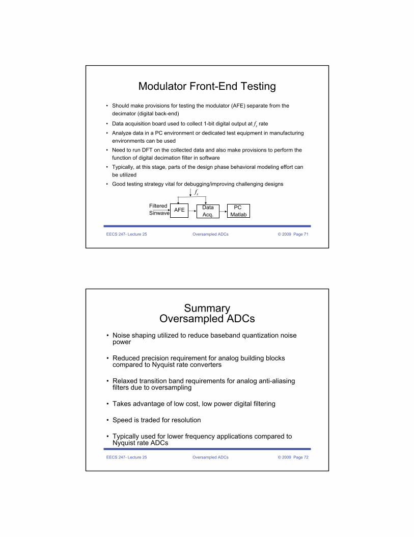
Modulator Front-End Testing• Should make provisions for testing the modulator (AFE) separate from the
decimator (digital back-end)
• Data acquisition board used to collect 1-bit digital output at fs rate
• Analyze data in a PC environment or dedicated test equipment in manufacturing environments can be used
• Need to run DFT on the collected data and also make provisions to perform the function of digital decimation filter in software
• Typically, at this stage, parts of the design phase behavioral modeling effort can be utilized
• Good testing strategy vital for debugging/improving challenging designs
AFE Data Acq.
PC Matlab
fs
FilteredSinwave
EECS 247- Lecture 25 Oversampled ADCs © 2009 Page 72
SummaryOversampled ADCs
• Noise shaping utilized to reduce baseband quantization noise power
• Reduced precision requirement for analog building blocks compared to Nyquist rate converters
• Relaxed transition band requirements for analog anti-aliasing filters due to oversampling
• Takes advantage of low cost, low power digital filtering
• Speed is traded for resolution
• Typically used for lower frequency applications compared to Nyquist rate ADCs


![A Novel Digital Calibration Technique for Gain and Offset ......ΣΔ modulators. The input signal x[n] is distributed among the M modulators through an analog multiplexer. Then, the](https://static.fdocument.org/doc/165x107/60ee77b99c0fd85f564bb9e6/a-novel-digital-calibration-technique-for-gain-and-offset-modulators.jpg)